ICGOO在线商城 > 集成电路(IC) > 线性 - 放大器 - 仪表,运算放大器,缓冲器放大器 > MAX4321EUK+T

 Datasheet下载
- 型号: MAX4321EUK+T
- 制造商: Maxim
- 库位|库存: xxxx|xxxx
- 要求:
| 数量阶梯 | 香港交货 | 国内含税 |
| +xxxx | $xxxx | ¥xxxx |
查看当月历史价格
查看今年历史价格
MAX4321EUK+T产品简介:
ICGOO电子元器件商城为您提供MAX4321EUK+T由Maxim设计生产,在icgoo商城现货销售,并且可以通过原厂、代理商等渠道进行代购。 MAX4321EUK+T价格参考¥14.35-¥27.26。MaximMAX4321EUK+T封装/规格:线性 - 放大器 - 仪表,运算放大器,缓冲器放大器, General Purpose Amplifier 1 Circuit Rail-to-Rail SOT-23-5。您可以下载MAX4321EUK+T参考资料、Datasheet数据手册功能说明书,资料中有MAX4321EUK+T 详细功能的应用电路图电压和使用方法及教程。
Maxim Integrated的MAX4321EUK+T是一款低功耗、单路运算放大器,属于线性放大器类别,采用SOT-23-5小型封装,适用于对空间和功耗敏感的应用场景。该器件具有宽电源电压范围(1.8V至5.5V)、低静态电流(典型值26μA)以及轨对轨输入输出特性,使其非常适合便携式和电池供电设备。

典型应用场景包括:便携式医疗设备(如血糖仪、心率监测器)、手持式测试仪器、传感器信号调理(如温度、压力、光强传感器的放大与缓冲)、工业控制中的低功耗模拟前端,以及消费类电子产品(如智能手机、可穿戴设备)中的信号放大与处理。其高精度和稳定性也适用于需要低噪声和低失调的模拟信号链设计。

此外,MAX4321EUK+T具备良好的驱动能力,可直接驱动容性负载,简化PCB布局设计。在多通道系统中,其小尺寸封装有助于提高集成度。整体而言,该器件广泛应用于需要低功耗、高性能和小型化的模拟放大场合。
| 参数 | 数值 |
| -3db带宽 | - |
| 产品目录 | 集成电路 (IC) |
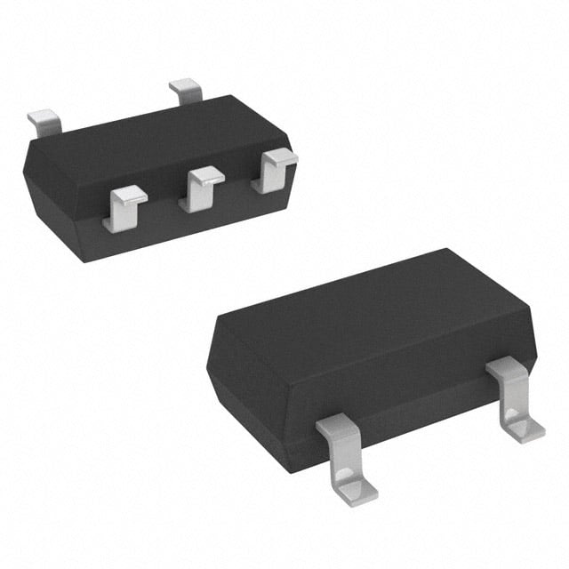
| 描述 | IC OPAMP GP 5MHZ RRO SOT23-5 |
| 产品分类 | Linear - Amplifiers - Instrumentation, OP Amps, Buffer Amps |
| 品牌 | Maxim Integrated |
| 数据手册 | |
| 产品图片 |
|
| 产品型号 | MAX4321EUK+T |
| rohs | 无铅 / 符合限制有害物质指令(RoHS)规范要求 |
| 产品系列 | - |
| 产品培训模块 | http://www.digikey.cn/PTM/IndividualPTM.page?site=cn&lang=zhs&ptm=25703http://www.digikey.cn/PTM/IndividualPTM.page?site=cn&lang=zhs&ptm=25705 |
| 产品目录页面 | |
| 供应商器件封装 | SOT-23-5 |
| 其它名称 | MAX4321EUK+T-ND |
| 包装 | 带卷 (TR) |
| 压摆率 | 2 V/µs |
| 增益带宽积 | 5MHz |
| 安装类型 | 表面贴装 |
| 封装/外壳 | SC-74A,SOT-753 |
| 工作温度 | -40°C ~ 85°C |
| 放大器类型 | 通用 |
| 标准包装 | 2,500 |
| 电压-电源,单/双 (±) | 2.4 V ~ 6.5 V, ±1.2 V ~ 3.25 V |
| 电压-输入失调 | 1.2mV |
| 电流-电源 | 725µA |
| 电流-输入偏置 | 50nA |
| 电流-输出/通道 | 50mA |
| 电路数 | 1 |
| 输出类型 | 满摆幅 |


- 商务部:美国ITC正式对集成电路等产品启动337调查
- 曝三星4nm工艺存在良率问题 高通将骁龙8 Gen1或转产台积电
- 太阳诱电将投资9.5亿元在常州建新厂生产MLCC 预计2023年完工
- 英特尔发布欧洲新工厂建设计划 深化IDM 2.0 战略
- 台积电先进制程称霸业界 有大客户加持明年业绩稳了
- 达到5530亿美元!SIA预计今年全球半导体销售额将创下新高
- 英特尔拟将自动驾驶子公司Mobileye上市 估值或超500亿美元
- 三星加码芯片和SET,合并消费电子和移动部门,撤换高东真等 CEO
- 三星电子宣布重大人事变动 还合并消费电子和移动部门
- 海关总署:前11个月进口集成电路产品价值2.52万亿元 增长14.8%


PDF Datasheet 数据手册内容提取
19-1649; Rev 0; 4/00 Low-Cost, Low-Voltage, Rail-to-Rail, Input/Output, SOT23 5MHz Op Amp General Description Features M The MAX4321 operational amplifier (op amp) combines ♦ Low-Voltage, Pin-for-Pin Upgrade for LMC7101 A a 5MHz gain-bandwidth product and excellent DC accuracy with Rail-to-Rail® operation at both the inputs ♦ Guaranteed +2.4V to +6.5V Single-Supply X and the output. This device requires only 650µA and Operation 4 operates from either a single +2.4V to +6.5V supply or ♦ Typically Operates Down to +1.8V 3 dual ±1.2V to ±3.25V supplies, although the MAX4321 typically operates down to +1.8V (±0.9V). The ♦ 5MHz Gain-Bandwidth Product 2 1 MAX4321 remains unity-gain stable with capacitive ♦ 650µA Quiescent Current loads up to 500pF and is capable of driving 250Ωloads to within 200mV of either rail. ♦ Rail-to-Rail Common-Mode Input Voltage Range With rail-to-rail input common-mode range and output ♦ Rail-to-Rail Output Voltage Range swing, the MAX4321 is ideal for low-voltage, single-sup- ♦ Drives 250ΩLoads ply applications. In addition, low ±1.2mV input offset volt- age and high 2V/µs slew rate make this device ideal for ♦ Unity-Gain Stable for Capacitive Loads up to signal-conditioning stages for precision, low-voltage data- 500pF acquisition systems. The MAX4321 comes in a space- ♦ No Phase Reversal for Overdriven Inputs saving 5-pin SOT23 package and is guaranteed over the extended (-40°C to +85°C) temperature range. ♦ Low-Cost Solution in SOT23-5 Package The MAX4321 is a low-voltage, pin-for-pin compatible upgrade for the LMC7101 that offers five-times higher bandwidth, two-times faster slew rate, and about half the input voltage noise density. ________________________Applications Ordering Information Battery-Powered Instruments TEMP. PIN- TOP PART Portable Equipment RANGE PACKAGE MARK Data-Acquisition Systems MAX4321EUK-T -40°C to +85°C 5 SOT23-5 ADOA Sensor and Signal Conditioning Low-Power, Low-Voltage Applications General-Purpose Low-Voltage Applications Pin Configuration/ Typical Operating Circuit Functional Diagram +5V TOP VIEW MAX187 3 1 OUT 1 5 VEE SHDN VDD 6 2 SERIAL DOUT AIN MAX4321 VCC 2 INTERFACE 8 4 SCLK VREF IN+ 3 4 IN- 7 5 CS GND MAX4321 SOT23 Rail-to-Rail is a registered trademark of Nippon Motorola, Ltd. ________________________________________________________________Maxim Integrated Products 1 For pricing, delivery, and ordering information, please contact Maxim Direct at 1-888-629-4642, or visit Maxim's website at www.maxim-ic.com.
Low-Cost, Low-Voltage, Rail-to-Rail, Input/Output, SOT23 5MHz Op Amp 1 ABSOLUTE MAXIMUM RATINGS 2 Supply Voltage (VCCto VEE)....................................-0.3V to +7V Operating Temperature Range...........................-40°C to +85°C 3 All Other Pins ..................................(VEE- 0.3V) to (VCC+ 0.3V) Junction Temperature......................................................+150°C Output Short-Circuit Duration.....................................Continuous Storage Temperature Range.............................-65°C to +150°C 4 (short to either supply) Lead Temperature (soldering, 10s)................................+300°C X Continuous Power Dissipation (TA= +70°C) 5-pin SOT23 (derate 7.1mW/°C above +70°C)...........571mW A M Stresses beyond those listed under “Absolute Maximum Ratings” may cause permanent damage to the device. These are stress ratings only, and functional operation of the device at these or any other conditions beyond those indicated in the operational sections of the specifications is not implied. Exposure to absolute maximum rating conditions for extended periods may affect device reliability. DC ELECTRICAL CHARACTERISTICS (VCC= +5.0V, VEE= 0, VCM= 0, VOUT= VCC/2, RL= ∞connected to VCC/2, TA= +25°C, unless otherwise noted.) PARAMETER SYMBOL CONDITIONS MIN TYP MAX UNITS Supply Voltage Range VCC - VEE 2.4 6.5 V VCC = +2.4V 650 Supply Current VCM = VOUT = VCC/2 µA VCC = +6.5V 725 Input Offset Voltage VOS VCM = VEE or VCC ±1.2 ±3.5 mV Input Bias Current IBIAS VCM = VEE or VCC ±50 ±150 nA Input Offset Current IOFFSET VCM = VEE or VCC ±4 ±25 nA Differential Input RIN -1.5V < VDIFF <+1.5V 500 kΩ Resistance Common-Mode Input Voltage VCM Inferred from CMRR test VEE VCC V Range Common-Mode Rejection CMRR VEE ≤ VCM ≤ VCC 60 91 dB Ratio Power-Supply Rejection Ratio PSRR 2.4V < VCC < 6.5V 66 100 dB Output Resistance ROUT AV = +1V/V 0.1 Ω VOUT = 0.25V to 4.75V, RL = 100kΩ 103 dB Large-Signal Voltage Gain AV VOUT = 0.40V to 4.60V, RL = 600Ω 100 VOUT = 0.40V to 4.60V, RL = 250Ω 70 86 RL = 100kΩ VCC - VOH 25 VOL - VEE 20 Output Voltage Swing VOUT RL = 600Ω VCC - VOH 135 mV VOL - VEE 60 RL = 250Ω VCC - VOH 200 300 VOL - VEE 100 200 Output Short-Circuit Current 50 mA 2 _______________________________________________________________________________________
Low-Cost, Low-Voltage, Rail-to-Rail, Input/Output, SOT23 5MHz Op Amp DC ELECTRICAL CHARACTERISTICS M (VCC= +5.0V, VEE= 0, VCM= 0, VOUT= VCC/2, RL= ∞connected to VCC/2, TA= -40°C to +85°C, unless otherwise noted.) (Note 1) A PARAMETER SYMBOL CONDITIONS MIN TYP MAX UNITS X Supply Voltage Range VCC - VEE 2.4 6.5 V 4 Supply Current ICC VCM = VOUT = VCC/2 1200 μA 3 Input Offset Voltage VOS VCM = VEE or VCC ±6 mV 2 Input Offset Voltage 1 ±2 μV/°C Temperature Coefficient Input Bias Current IBIAS VCM = VEE or VCC ±180 nA Input Offset Current IOFFSET VCM = VEE or VCC ±50 nA Common-Mode Input Voltage VCM Inferred from CMRR test VEE VCC V Range Common-Mode Rejection Ratio CMRR VEE ≤ VCM ≤ VCC 54 dB Power-Supply Rejection Ratio PSRR 2.4V < VCC < 6.5V 62 dB Large-Signal Voltage Gain AV VOUT = 0.40V to 4.60V, RL = 250Ω 66 dB Output Voltage Swing VOUT R = 250Ω VCC - VOH 350 mV VOL - VEE 250 AC ELECTRICAL CHARACTERISTICS (VCC= +5.0V, VEE= 0, VCM= 0, VOUT= VCC/2, RL= 250Ωconnected to VCC/2, TA= +25°C, unless otherwise noted.) PARAMETER SYMBOL CONDITIONS MIN TYP MAX UNITS Gain-Bandwidth Product GBP 5 MHz Phase Margin 64 degrees Gain Margin 12 dB Total Harmonic Distortion 10kHz tone, VOUT = 2Vpp, THD+N 0.003 % and Noise AV = +1V/V Slew Rate SR VOUT = 1V step 2 V/μs Settling Time to 0.01% tSETTLE VOUT = 2V step, AV = +1V/V 2 μs Turn-On Time tON VCC = 0 to 3V step 1 μs Input Capacitance CIN 3 pF Input Noise Voltage Density f = 1kHz 22 nV/√ Hz Input Noise Current Density f = 1kHz 0.4 pA/√Hz Note 1:All devices are 100% production tested at TA= +25°C. All temperature limits are guaranteed by design and characterization. _______________________________________________________________________________________ 3
Low-Cost, Low-Voltage, Rail-to-Rail, Input/Output, SOT23 5MHz Op Amp 1 Typical Operating Characteristics 2 (VCC= +5V, VEE= 0, VCM= VCC/2, TA= +25°C, unless otherwise noted.) 3 4 GAIN AND PHASE vs. FREQUENCY POWER-SUPPLY REJECTION X GAIN AND PHASE vs. FREQUENCY (WITH CLOAD) vs. FREQUENCY MA 60 MAX4321-01118404 60 MAX4321-02 118404 0 AV = +1 MAX4321-03 40 108 40 GAIN 108 -20 GAIN (dB)200 PHASE GAIN 70-33266PHASE (DEGREES) GAIN (dB)200 PHASE 0-733266 PHASE (DEGREES) PSR (dB)--6400 -72 -72 -80 -20 AV = +1000 -108 -20 ARVL == ∞+1000 -108 NO LOAD -144 CL = 500pF -144 -100 -40 -180 -40 -180 100 1k 10k 100k 1M 10M 100M 100 1k 10k 100k 1M 10M 100M 10 100 1k 10k 100k 1M 10M 100M FREQUENCY (Hz) FREQUENCY (Hz) FREQUENCY (Hz) OUTPUT IMPEDANCE INPUT OFFSET VOLTAGE vs. FREQUENCY SUPPLY CURRENT vs. TEMPERATURE vs. TEMPERATURE 100 AV = +1 MAX4321-04 980500 MAX4321-05 23..2050 MAX4321-06 ΩOUTPUT IMPEDANCE () 01.101 μSUPPLY CURRENT (A) 667780505000000 VVCCCC == 62..57VV VOLTAGE (mV)--1001....577500550 550 -2.25 0.01 500 -3.00 100 1k 10k 100k 1M 10M 100M -40 -25 -10 5 20 35 50 65 80 95 -40 -25 -10 5 20 35 50 65 80 95 FREQUENCY (Hz) TEMPERATURE (°C) TEMPERATURE (°C) INPUT BIAS CURRENT INPUT BIAS CURRENT COMMON-MODE REJECTION vs. COMMON-MODE VOLTAGE vs. TEMPERATURE vs. TEMPERATURE INPUT BIAS CURRENT (nA) ---12345321000000000 VCC = 2.7V VCC = 6.5V MAX4321-07 INPUT BIAS CURRENT (nA) ----4512343210000000000 VCC = 2.7V, VCM V= CVCC C=V 2C.7CV =, 6V.C5MV ,= V VCEME = VCC MAX4321-08 COMMON-MODE REJECTION (dB) 1111199200110500505 VCM = -0.2V TOV C5M.2 =V 0 TO 5.0V MAX4321-09 -40 -50 VCC = 6.5V, VCM = VEE 85 -50 -60 80 0 1 2 3 4 5 6 -40 -25 -10 5 20 35 50 65 80 95 -40 -25 -10 5 20 35 50 65 80 95 COMMON-MODE VOLTAGE (V) TEMPERATURE (°C) TEMPERATURE (°C) 4 _______________________________________________________________________________________
Low-Cost, Low-Voltage, Rail-to-Rail, Input/Output, SOT23 5MHz Op Amp Typical Operating Characteristics (continued) M (VCC= +5V, VEE= 0, VCM= VCC/2, TA= +25°C, unless otherwise noted.) A X MINIMUM OUTPUT VOLTAGE MAXIMUM OUTPUT VOLTAGE LARGE-SIGNAL GAIN 4 vs. TEMPERATURE vs. TEMPERATURE vs. OUTPUT VOLTAGE 3 250 RL TO VCC MAX4321-10 235000 RL TO VEE MAX4321-11 112100 VRCLC T =O 2V.7EEV RL = 100kΩ MAX4321-12 21 200 VCC = 6.5V, RL = 500Ω VCC = 6.5V, RL = 500Ω V- V(mV)OUT EE 115000 VCC = 2.7V, RL = 500Ω V - V (mV)CCOUT 112050000 VCC = 2.7V, RL = 500Ω GAIN (dB) 1980000 RL = 5R0L0 =ΩR 2Lk =Ω 10kΩ 50 VCC = 6.5V, RL = 100kΩ 50 VCC = 6.5V, RL = 100kΩ (TOP) 70 VCC = 2.7V, RL = 100kΩ (BOTTOM) VCC = 2.7V, RL = 100kΩ 0 0 60 -40 -25 -10 5 20 35 50 65 80 95 -40 -25 -10 5 20 35 50 65 80 95 0 100 200 300 400 500 600 TEMPERATURE (°C) TEMPERATURE (°C) OUTPUT VOLTAGE: FROM VCC (mV) LARGE-SIGNAL GAIN LARGE-SIGNAL GAIN LARGE-SIGNAL GAIN vs. OUTPUT VOLTAGE vs. OUTPUT VOLTAGE vs. OUTPUT VOLTAGE 120 120 120 110 VRCLC T =O 6V.5EEV MAX4321-13 110 VRCL CT O= V2.C7CV RL = 100kΩ MAX4321-14 110 VRCL CT O= 6V.C5CV RL = 100kΩ MAX4321-15 RL = 100kΩ RL = 10kΩ RL = 10kΩ 100 RL = 10kΩ 100 100 RL = 2kΩ N (dB) 90 RL = 2kΩ N (dB) 90 RL = 2kΩ N (dB) 90 GAI GAI GAI RL = 500Ω 80 80 RL = 500Ω 80 RL = 500Ω 70 70 70 60 60 60 0 100 200 300 400 500 600 0 100 200 300 400 500 600 0 100 200 300 400 500 600 OUTPUT VOLTAGE: FROM VCC (mV) OUTPUT VOLTAGE: FROM VEE (mV) OUTPUT VOLTAGE: FROM VEE (mV) LARGE-SIGNAL GAIN LARGE-SIGNAL GAIN MINIMUM OPERATING VOLTAGE vs. TEMPERATURE vs. TEMPERATURE vs. TEMPERATURE 111212550 RVLO U=T 5(p0-0pΩ) = VCC - 1V VRCL CT O= V6.E5EV, MAX4321-16 111221505 VCC = 6.V5VC,C R =L 6T.O5V V, EREL TO VCC MAX4321-17 E (V) 11..89 MAX4321-18 G 110 VRCL CT O= V2.E7EV, 110 VOLTA 1.7 GAIN (dB) 11900550 GAIN (dB) 11900550 VCC = 2.7V, RL TO VEE PERATING 11..56 VCC = 6.5V, RL TO VCC VCC = 2.7V, RL TO VCC M O 90 90 U 1.4 M 85 85 VOUT(p-p) = VCC - 600mV MINI 1.3 80 VCC = 2.7V, RL TO VCC 80 RL = 100kΩ 75 75 1.2 -40 -25 -10 5 20 35 50 65 80 95 -40 -25 -10 5 20 35 50 65 80 95 -40 -25 -10 5 20 35 50 65 80 95 TEMPERATURE (°C) TEMPERATURE (°C) TEMPERATURE (°C) _______________________________________________________________________________________ 5
Low-Cost, Low-Voltage, Rail-to-Rail, Input/Output, SOT23 5MHz Op Amp 1 Typical Operating Characteristics (continued) 2 (VCC= +5V, VEE= 0, VCM= VCC/2, TA= +25°C, unless otherwise noted.) 3 4 TOTAL HARMONIC DISTORTION TOTAL HARMONIC DISTORTION PLUS NOISE SMALL-SIGNAL TRANSIENT X PLUS NOISE vs. FREQUENCY vs. PEAK-TO-PEAK SIGNAL AMPLITUDE RESPONSE (NONINVERTING) MA 00..004305 A2VV p=- p+ 1SIGNAL MAX4321-19 0.1 A1R0VL k T H=O z+ VS1CINCE / W2AVE MAX4321-20 AV = +1 MAX4321-21 THD + NOISE (%) 0000....000012235050 5R0L 0=k H10z kLΩO WTOP AVSCSC F/ I2LTER THD + NOISE (%) 0.01 5FI0L0TRkELHR =z L2O50WΩPASS RL = 2kΩ VOLTAGE50mV/divIN 0.010 OUT RL = 10kΩ RL = 100kΩ 0.005 0 0.001 10 100 1k 10k 100k 4.0 4.2 4.4 4.6 4.8 5.0 200ns/div FREQUENCY (Hz) PEAK-TO-PEAK SIGNAL AMPLITUDE (V) LARGE-SIGNAL TRANSIENT LARGE-SIGNAL TRANSIENT SMALL-SIGNAL TRANSIENT RESPONSE (INVERTING) RESPONSE (NONINVERTING) RESPONSE (INVERTING) AV = -1 MAX4321-22 AV = +1 MAX4321-23 AV = -1 MAX4321-24 IN IN IN VOLTAGE 50mV/div VOLTAGE2V/div VOLTAGE2V/div OUT OUT OUT 200ns/div 2μs/div 2μs/div Pin Description PIN NAME FUNCTION 1 OUT Output 2 VCC Positive Supply 3 IN+ Noninverting Input 4 IN- Inverting Input 5 VEE Negative Supply. Connect to ground for single-supply operation. 6 _______________________________________________________________________________________
Low-Cost, Low-Voltage, Rail-to-Rail, Input/Output, SOT23 5MHz Op Amp __________Applications Information rents flowing through external source impedances, M match the effective impedance seen by each input Rail-to-Rail Input Stage (Figures 1a, 1b). High source impedances, together A The MAX4321 high-speed amplifier has rail-to-rail input with the input capacitance, can create a parasitic pole X and output stages designed for low-voltage, single- that produces an underdamped signal response. 4 supply operation. The input stage consists of separate Reducing the input impedance or placing a small (2pF NPN and PNP differential stages, which combine to to 10pF) capacitor across the feedback resistor 3 provide an input common-mode range extending to the improves the response. 2 supply rails. The PNP stage is active for input voltages The MAX4321’sinputs are protected from large differen- 1 close to the negative rail, and the NPN stage is active tial input voltages by 1kΩ series resistors and back-to- for input voltages near the positive rail. The switchover back triple diodes across the inputs (Figure 2). For transition region, which occurs near VCC / 2, has been differential input voltages less than 1.8V, the input resis- extended to minimize the slight degradation in CMRR tance is typically 500kΩ. For differential input voltages caused by the mismatch of the input pairs. Its low offset greater than 1.8V, the input resistance is approximately voltage, high bandwidth, and rail-to-rail common-mode 2kΩ, and the input bias current is determined by the fol- range makes this op amp an excellent choice for preci- lowing equation: sion, low-voltage, data-acquisition systems. Since the input stage switches between the NPN and V - 1.8V PNP pairs, the input bias current changes polarity as I = DIFF the input voltage passes through the transition region. BIAS 2kΩ To reduce the offset error caused by input bias cur- R3 R3 MAX4321 MAX4321 R1 R2 R1 R2 R3 = R1 R2 R3 = R1 R2 Figure 1a. Reducing Offset Error Due to Bias Current Figure 1b. Reducing Offset Error Due to Bias Current (Noninverting) (Inverting) 1k 1k Figure 2. Input Protection Circuit _______________________________________________________________________________________ 7
Low-Cost, Low-Voltage, Rail-to-Rail, Input/Output, SOT23 5MHz Op Amp 1 Rail-to-Rail Output Stage Driving a capacitive load can cause instability in most The minimum output voltage will be within millivolts of high-speed op amps, especially those with low quies- 2 ground for single-supply operation where the load is cent current. The MAX4321 has a high tolerance for 3 referenced to ground (VEE). Figure 3 shows the input capacitive loads. It is stable with capacitive loads up to 4 voltage range and output voltage swing of a MAX4321 500pF. Figure 4 gives the stable operating region for X connected as a voltage follower. With a +3V supply capacitive loads. Figures 5 and 6 show the response A and the 100kΩ load tied to ground, the output swings with capacitive loads and the results of adding an isola- from 0.02V to 2.97V. The maximum output voltage tion resistor in series with the output (Figure 7). The M swing depends on the load but will be within 300mV of resistor improves the circuit’s phase margin by isolating a +5V supply, even with the maximum load (250Ω to the load capacitor from the op amp’s output. ground). 10,000 VCC = 3V IN AV = +1 UNSTABLE F) REGION p E ( VOLTAGE1V/div CAPACITIV1000 OUT D A O L RL TO VEE RL = 100kΩ VOUT = VCC / 2 100 2μs/div 100 1k 10k 100k RESISTIVE LOAD (Ω) Figure 3. Rail-to-Rail Input /Output Voltage Range Figure 4. Capacitive-Load Stability AV = +1 AV = +1 CL = 500pF CRSL == 3190Ω00pF IN IN VOLTAGE50mV/div VOLTAGE50mV/div OUT OUT 400ns/div 400ns/div Figure 5. Small-Signal Transient Response with Capacitive Figure 6. Transient Response to Capacitive Load with Isolation Load Resistor 8 _______________________________________________________________________________________
Low-Cost, Low-Voltage, Rail-to-Rail, Input/Output, SOT23 5MHz Op Amp Power-Up Good layout improves performance by decreasing the M The MAX4321typically settles within 1µs after power-up. amount of stray capacitance at the op amp’s inputs Using the test circuit of Figure 8, Figures 9 and 10 show and outputs. To decrease stray capacitance, minimize A the output voltage and supply current on power-up. trace lengths and resistor leads by placing external X components close to the op amp’s pins. Power Supplies and Layout 4 The MAX4321 operates from single +2.4V to +6.5V or Package Information 3 dual ±1.2V to ±3.25V supplies, though it typically oper- 2 ates down to +1.8V (±0.9V). For single-supply opera- TRANSISTOR COUNT: 84 1 tion, bypass the power supply with a 0.1µF ceramic capacitor in parallel with at least 1µF. For dual supplies, bypass each supply to ground. VCC MAX4321 0V TO 2.7V STEP FOR POWER-UP RS TEST 2k VOUT CL MAX4321 SUPPLY-CURRENT 2k 10Ω MONITORING POINT 10k Figure 7. Capacitive-Load-Driving Circuit Figure 8. Power-Up Test Circuit VCC VCC 1V/div E LTAGV/div O1 V OUT ICC 500μA/div 5μs/div 5μs/div Figure 9. Power-Up Output Voltage Figure 10. Power-Up Supply Current _______________________________________________________________________________________ 9
Low-Cost, Low-Voltage, Rail-to-Rail, Input/Output, SOT23 5MHz Op Amp 1 Package Information 2 3 S P 4 L .E 5 X 3 2 T- A O S M 10 ______________________________________________________________________________________
Low-Cost, Low-Voltage, Rail-to-Rail, Input/Output, SOT23 5MHz Op Amp NOTES M A X 4 3 2 1 ______________________________________________________________________________________ 11
Low-Cost, Low-Voltage, Rail-to-Rail, Input/Output, SOT23 5MHz Op Amp 1 NOTES 2 3 4 X A M Maxim cannot assume responsibility for use of any circuitry other than circuitry entirely embodied in a Maxim product. No circuit patent licenses are implied. Maxim reserves the right to change the circuitry and specifications without notice at any time. 12 ____________________Maxim Integrated Products, 120 San Gabriel Drive, Sunnyvale, CA 94086 408-737-7600 © 2000 Maxim Integrated Products is a registered trademark of Maxim Integrated Products, Inc.