ICGOO在线商城 > 集成电路(IC) > 线性 - 放大器 - 仪表,运算放大器,缓冲器放大器 > MAX4219EEE+

 Datasheet下载
- 型号: MAX4219EEE+
- 制造商: Maxim
- 库位|库存: xxxx|xxxx
- 要求:
| 数量阶梯 | 香港交货 | 国内含税 |
| +xxxx | $xxxx | ¥xxxx |
查看当月历史价格
查看今年历史价格
MAX4219EEE+产品简介:
ICGOO电子元器件商城为您提供MAX4219EEE+由Maxim设计生产,在icgoo商城现货销售,并且可以通过原厂、代理商等渠道进行代购。 MAX4219EEE+价格参考。MaximMAX4219EEE+封装/规格:线性 - 放大器 - 仪表,运算放大器,缓冲器放大器, 缓冲器 放大器 3 电路 满摆幅 16-QSOP。您可以下载MAX4219EEE+参考资料、Datasheet数据手册功能说明书,资料中有MAX4219EEE+ 详细功能的应用电路图电压和使用方法及教程。
MAX4219EEE+ 是 Maxim Integrated 公司生产的一款低功耗、高精度仪表放大器,属于线性放大器类别中的仪表放大器系列。其主要应用场景包括以下几方面:

 1. 医疗设备
   - 心电图(ECG)和脑电图(EEG)监测:MAX4219EEE+ 的高共模抑制比(CMRR)和低噪声特性使其非常适合用于生物电位信号的放大,能够准确捕捉微弱的心电信号或脑电信号。
   - 血压监测仪:可用于放大压力传感器输出的微小信号,提高测量精度。

 2. 工业自动化
   - 传感器信号调理:在工业控制中,常用于放大来自温度、压力、应变等传感器的信号,同时抑制环境噪声干扰。
   - 数据采集系统:作为前端放大器,将传感器的微弱信号放大到适合模数转换(ADC)的电平范围。

 3. 测试与测量
   - 精密测量仪器:如数字万用表(DMM),需要对极小的电压或电流变化进行精确测量,MAX4219EEE+ 的高增益精度和低失调电压特性非常适合此类应用。
   - 信号分析仪:用于放大待测信号,确保后续处理的准确性。

 4. 音频设备
   - 低噪声前置放大器:适用于麦克风或其他音频输入信号的放大,提供清晰且失真小的音频信号。

 5. 汽车电子
   - 胎压监测系统(TPMS):用于放大压力传感器输出信号,确保轮胎压力的精确监测。
   - 车载诊断系统(OBD):放大传感器信号以实现车辆状态的实时监控。

 6. 消费电子产品
   - 可穿戴设备:如智能手表或健康手环,用于放大人体生理信号(如心率、血氧等)。
   - 智能家居传感器:例如温湿度传感器信号放大,提升环境监测的灵敏度。

 特性优势
- 低功耗:适合电池供电的便携式设备。
- 高共模抑制比(CMRR):有效抑制噪声干扰,特别是在嘈杂的工业环境中。
- 高增益精度:确保信号放大的一致性,适用于精密测量场合。
- 宽工作电压范围:支持多种电源配置,适应不同应用场景。

综上所述,MAX4219EEE+ 凭借其优异的性能,广泛应用于需要高精度、低噪声和低功耗信号放大的领域。
| 参数 | 数值 |
| -3db带宽 | 200MHz |
| 产品目录 | 集成电路 (IC)半导体 |
| 描述 | IC OPAMP BUFFER 200MHZ 16QSOP高速运算放大器 Closed-Loop Rail-Rail Buffer |
| 产品分类 | Linear - Amplifiers - Instrumentation, OP Amps, Buffer Amps集成电路 - IC |
| 品牌 | Maxim Integrated |
| 产品手册 | |
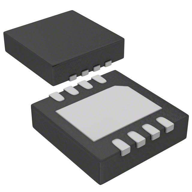
| 产品图片 |
|
| rohs | 符合RoHS无铅 / 符合限制有害物质指令(RoHS)规范要求 |
| 产品系列 | 放大器 IC,高速运算放大器,Maxim Integrated MAX4219EEE+- |
| 数据手册 | |
| 产品型号 | MAX4219EEE+ |
| 产品 | Voltage Feedback Amplifier |
| 产品培训模块 | http://www.digikey.cn/PTM/IndividualPTM.page?site=cn&lang=zhs&ptm=25703http://www.digikey.cn/PTM/IndividualPTM.page?site=cn&lang=zhs&ptm=25705 |
| 产品目录页面 | |
| 产品种类 | |
| 供应商器件封装 | 16-QSOP |
| 包装 | 管件 |
| 压摆率 | 600 V/µs |
| 商标 | Maxim Integrated |
| 增益带宽积 | - |
| 安装类型 | 表面贴装 |
| 安装风格 | SMD/SMT |
| 封装 | Tube |
| 封装/外壳 | 16-SSOP(0.154",3.90mm 宽) |
| 封装/箱体 | QSOP-16 |
| 工作温度 | -40°C ~ 85°C |
| 工作电源电压 | 5 V, 9 V |
| 工厂包装数量 | 100 |
| 拓扑结构 | Voltage Feedback |
| 放大器类型 | 缓冲器 |
| 最大功率耗散 | 667 mW |
| 最大工作温度 | + 85 C |
| 最小工作温度 | - 40 C |
| 标准包装 | 1 |
| 电压-电源,单/双 (±) | 3.15 V ~ 11 V, ±1.575 V ~ 5.5 V |
| 电压-输入失调 | 4mV |
| 电压增益dB | 6.02 dB |
| 电流-电源 | 5.5mA |
| 电流-输入偏置 | 5.4µA |
| 电流-输出/通道 | 120mA |
| 电源电压-最大 | 11 V |
| 电源电压-最小 | 3.15 V |
| 电源电流 | 400 uA |
| 电路数 | 3 |
| 系列 | MAX4219 |
| 转换速度 | 600 V/us |
| 输入补偿电压 | 4 mV at 5V |
| 输出类型 | 满摆幅 |
| 通道数量 | 3 Channel |
| 零件号别名 | MAX4219 |


- 商务部:美国ITC正式对集成电路等产品启动337调查
- 曝三星4nm工艺存在良率问题 高通将骁龙8 Gen1或转产台积电
- 太阳诱电将投资9.5亿元在常州建新厂生产MLCC 预计2023年完工
- 英特尔发布欧洲新工厂建设计划 深化IDM 2.0 战略
- 台积电先进制程称霸业界 有大客户加持明年业绩稳了
- 达到5530亿美元!SIA预计今年全球半导体销售额将创下新高
- 英特尔拟将自动驾驶子公司Mobileye上市 估值或超500亿美元
- 三星加码芯片和SET,合并消费电子和移动部门,撤换高东真等 CEO
- 三星电子宣布重大人事变动 还合并消费电子和移动部门
- 海关总署:前11个月进口集成电路产品价值2.52万亿元 增长14.8%


PDF Datasheet 数据手册内容提取
19-4754; Rev 1; 8/01 High-Speed, Single-Supply, Gain of 2, Closed-Loop, Rail-to-Rail Buffers with Enable _________________General Description ____________________________Features M The MAX4214/MAX4215/MAX4217/MAX4219/MAX4222 (cid:2) Internal Precision Resistors for Closed-Loop A are precision, closed-loop, gain of +2 (or -1) buffers Gains of +2V/V or -1V/V X featuring high slew rates, high output current drive, and (cid:2) High Speed low differential gain and phase error. They operate with 4 230MHz -3dB Bandwidth a single 3.15V to 11V supply or with ±1.575V to ±5.5V 2 dual supplies. The input common-mode voltage range 90MHz 0.1dB Gain Flatness 1 extends 100mV beyond the negative power-supply rail, (MAX4219/MAX4222) and the output swings Rail-to-Rail®. 600V/µs Slew Rate 4 / These devices require only 5.5mA of quiescent supply (cid:2) Single 3.3V/5.0V Operation M current while achieving a 230MHz -3dB bandwidth and (cid:2) Outputs Swing Rail-to-Rail A a 600V/µs slew rate. In addition, the MAX4215/ MAX4219 have a disable feature that reduces the sup- (cid:2) Input Common-Mode Range Extends Beyond VEE X ply current to 400µA per buffer. Input voltage noise is (cid:2) Low Differential Gain/Phase Error: 0.03%/0.04° 4 only 10nV/√Hz, and input current noise is only 1.3pA/√Hz. This buffer family is ideal for low-power/low- (cid:2) Low Distortion at 5MHz 2 voltage applications requiring wide bandwidth, such as -72dBc SFDR 1 video, communications, and instrumentation systems. -71dB Total Harmonic Distortion 5 For space-sensitive applications, the MAX4214 comes (cid:2) High Output Drive: ±120mA / M in a miniature 5-pin SOT23 package. (cid:2) Low 5.5mA Supply Current A (cid:2) 400µA Shutdown Supply Current _______________Ordering Information X (MAX4215/MAX4219) PIN- TOP (cid:2) Space-Saving SOT23, µMAX, or QSOP Packages 4 PART TEMP RANGE PACKAGE MARK 2 1 MAX4214EUK-T -40°C to +85°C 5 SOT23-5 ABAH ______________________Selector Guide 7 MAX4215ESA -40°C to +85°C 8 SO — MAX4215EUA -40°C to +85°C 8 µMAX — PART NO. OF ENABLE PIN-PACKAGE /M AMPS MAX4217ESA -40°C to +85°C 8 SO — MAX4217EUA -40°C to +85°C 8 µMAX — MAX4214 1 No 5 SOT23 A MAX4219ESD -40°C to +85°C 14 SO — MAX4215 1 Yes 8 SO/µMAX X MAX4219EEE -40°C to +85°C 16 QSOP — MAX4217 2 No 8 SO/µMAX 4 MAX4222ESD -40°C to +85°C 14 SO — MAX4219 3 Yes 14 SO, 16 QSOP 2 MAX4222EEE -40°C to +85°C 16 QSOP — MAX4222 4 No 14 SO, 16 QSOP 1 9 ________________________Applications __________________Pin Configurations / M Battery-Powered Instruments A TOP VIEW Video Line Drivers X Analog-to-Digital Converter Interface OUT 1 5 VCC 4 CCD Imaging Systems 2 MAX4214 Video Routing and Switching Systems VEE 2 2 Video Multiplexing Applications 2 IN+ 3 4 IN- Typical Application Circuit appears at end of data sheet. SOT23-5 Rail-to-Rail is a registered trademark of Nippon Motorola, Ltd. Pin Configurations continued at end of data sheet. ________________________________________________________________Maxim Integrated Products 1 For pricing, delivery, and ordering information,please contact Maxim/Dallas Direct!at 1-888-629-4642, or visit Maxim’s website at www.maxim-ic.com.
High-Speed, Single-Supply, Gain of 2, Closed-Loop, Rail-to-Rail Buffers with Enable 2 ABSOLUTE MAXIMUM RATINGS 2 Supply Voltage (VCCto VEE)..................................................12V 8-Pin µMAX (derate 4.1mW/°C above +70°C).............330mW 2 IN_-, IN_+, OUT_, EN_ ....................(VEE- 0.3V) to (VCC+ 0.3V) 14-Pin SO (derate 8.3mW/°C above +70°C)................667mW 4 Output Short-Circuit Duration to VCCor VEE..............Continuous 16-Pin QSOP (derate 8.3mW/°C above +70°C)...........667mW Continuous Power Dissipation (TA= +70°C) Operating Temperature Range...........................-40°C to +85°C X 5-Pin SOT23 (derate 7.1mW/°C above +70°C).............571mW Storage Temperature Range.............................-65°C to +150°C 8-Pin SO (derate 5.9mW/°C above +70°C)...................471mW Lead Temperature (soldering, 10s).................................+300°C A M Stresses beyond those listed under “Absolute Maximum Ratings” may cause permanent damage to the device. These are stress ratings only, and functional operation of the device at these or any other conditions beyond those indicated in the operational sections of the specifications is not implied. Exposure to / absolute maximum rating conditions for extended periods may affect device reliability. 9 1 DC ELECTRICAL CHARACTERISTICS 2 4 (VCC = 5V, VEE = 0, IN_- = 0, EN_ = 5V, RL = ∞ to 0, VOUT = VCC/2, noninverting configuration, TA = TMIN to TMAX, unless X otherwise noted. Typical values are at TA= +25°C.) (Note 1) PARAMETER SYMBOL CONDITIONS MIN TYP MAX UNITS A Operating Supply Voltage M VCCto VEE, guaranteed by PSRR tests 3.15 11.0 V Range 7/ IN_+ VEE- 0.1 VCC- 2.25 Input Voltage Range VIN V 1 IN_- VEE- 0.1 VCC+ 0.1 2 Input Offset Voltage VOS RL= 50Ω SO, QSOP 4 10 mV 4 SOT23-5, µMAX 4 15 X Input Offset Voltage Drift TCVOS 8 µV/°C A Input Offset Voltage Between any two channels for 1 mV Matching MAX4217/MAX4219/MAX4222 M Input Bias Current IB IN_+ 5.4 12 µA 5/ Input Resistance RIN IN_+, over input voltage range 3 MΩ 1 Voltage Gain AV RL≥50Ω, (VEE+ 0.5V) ≤VOUT≤(VCC- 2.0V) 1.9 2 2.1 V/V 2 Power-Supply VCC= 5V, VEE= 0, VOUT= 2.0V 55 58 4 Rejection Ratio PSRR VCC= 5V, VEE= -5V, VOUT= 0 60 66 dB X (Note 2) VCC= 3.3V, VEE= 0, VOUT= 0.90V 45 A Output Resistance ROUT f = DC 25 mΩ M Output Current IOUT RL= 20Ωto VCCor VEE TA= +25°C ±70 ±120 mA TA= TMINto TMAX ±60 / Short-Circuit Output 4 ISC Sinking or sourcing ±150 mA Current 1 2 RL= 50Ω VCC- VOH 1.60 1.90 4 VOL- VEE 0.04 0.075 X Output Voltage Swing VOUT RL= 150Ω VCC- VOH 0.75 1.00 V VOL- VEE 0.04 0.075 A M RL= 2kΩ VCC- VOH 0.06 VOL- VEE 0.06 Disabled Output ROUT(OFF) MAX4215/MAX4219, EN_ = 0, 0 ≤VOUT≤5V 1 kΩ Resistance EN_ Logic Low Threshold VIL MAX4215/MAX4219 VCC- 2.6 V EN_ Logic High Threshold VIH MAX4215/MAX4219 VCC- 1.6 V 2 _______________________________________________________________________________________
High-Speed, Single-Supply, Gain of 2, Closed-Loop, Rail-to-Rail Buffers with Enable DC ELECTRICAL CHARACTERISTICS (continued) M (VCC = 5V, VEE = 0, IN_- = 0, EN_ = 5V, RL = ∞ to 0, VOUT = VCC/2, noninverting configuration, TA = TMIN to TMAX, unless A otherwise noted. Typical values are at TA= +25°C.) (Note 1) X PARAMETER SYMBOL CONDITIONS MIN TYP MAX UNITS EN_ Logic Input Low MAX4215/MAX4219, (VEE+ 0.2V) ≤EN_ ≤VCC 0.5 4 IIL µA 2 Current MAX4215/MAX4219, EN_ = VEE 200 350 1 EN_ Logic Input High IIH MAX4215/MAX4219, EN_ = VCC 0.5 10 µA 4 Current / Quiescent Supply M ICC 5.5 7.0 mA Current (per Buffer) A Shutdown Supply Current ISD MAX4215/MAX4219, disabled (EN_ = VEE) 400 550 µA X Note 1: The MAX421_EU_ is 100% production tested at TA= 25°C. Specifications over temperature limits are guaranteed by design. Note 2: PSRR for single 5V supply tested with VEE= 0, VCC= 4.5V to 5.5V; for dual ±5V supply with VEE= -4.5V to -5.5V, 4 VCC= 4.5V to 5.5V; and for single 3V supply with VEE= 0, VCC= 3.15V to 3.45V. 2 1 AC ELECTRICAL CHARACTERISTICS 5 (VCC= 5V, VEE= 0, IN_- = 0, EN_ = 5V, RL= 100Ωto VCC/2, noninverting configuration, TA= TMINto TMAX, unless otherwise noted. / Typical values are at TA= +25°C.) M PARAMETER SYMBOL CONDITIONS MIN TYP MAX UNITS A SBmanadllw-Sidigtnhal -3dB BW-3dB V10O0UmTV=P-P MMAAXX44221194//MMAAXX44222125/MAX4217 223000 MHz X4 Full-Power -3dB FPBW VOUT= MAX4214/MAX4215/MAX4217 220 MHz 2 Bandwidth 2VP-P MAX4219/MAX4222 200 1 BFlaantndewsisdth for 0.1dB Gain BW0.1dB V10O0UmTV=P-P MMAAXX44221194//MMAAXX44222125/MAX4217 9500 MHz 7/ M Slew Rate SR VOUT= 2V step 600 V/µs Settling Time to 0.1% tS VOUT= 2V step 45 ns A Rise/Fall Time tR, tF VOUT= 100mVP-P 1 ns X Spurious-Free Dynamic SFDR fC= 5MHz, VOUT= 2VP-P -72 dBc 4 Range 2 Second harmonic -72 1 Harmonic Distortion HD VOUT= 2VP-P, Third harmonic -77 dBc fC= 5MHz 9 Total harmonic distortion -71 / M Third-Order Intercept IP3 f = 10MHz 35 dBm Input 1dB Compression A f = 10MHz 11 dBm Point X Differential Phase Error DP NTSC, RL= 150Ω 0.04 degrees 4 Differential Gain Error DG NTSC, RL= 150Ω 0.03 % 2 Input Noise-Voltage en f = 10kHz 10 nV/√Hz 2 Density 2 Input Noise-Current in f = 10kHz 1.3 pA/√Hz Density Input Capacitance CIN 1 pF Disabled Output COUT(OFF) MAX4215/MAX4219, EN_ = 0 2 pF Capacitance _______________________________________________________________________________________ 3
High-Speed, Single-Supply, Gain of 2, Closed-Loop, Rail-to-Rail Buffers with Enable 2 AC ELECTRICAL CHARACTERISTICS (continued) 2 (VCC= 5V, VEE= 0, IN_- = 0, EN_ = 5V, RL= 100Ωto VCC/2, noninverting configuration, TA= TMINto TMAX, unless otherwise noted. 2 Typical values are at TA= +25°C.) 4 PARAMETER SYMBOL CONDITIONS MIN TYP MAX UNITS X Output Impedance ZOUT f = 10MHz 200 mΩ A Buffer Enable Time tON MAX4215/MAX4219 100 ns M Buffer Disable Time tOFF MAX4215/MAX4219 1 µs MAX4217/MAX4219/MAX4222, f = 10MHz, / Buffer Gain Matching 0.1 dB 9 VOUT= 100mVP-P 1 MAX4217/MAX4219/MAX4222, f = 10MHz, 2 All-Hostile Crosstalk XTALK VOUT= 2VP-P -95 dB 4 X A __________________________________________Typical Operating Characteristics M (VCC= 5V, VEE= 0, AVCL= 2V/V, RL= 100Ωto VCC/2, TA= +25°C, unless otherwise noted.) / 7 1 MAX4214/MAX4215/MAX4217 MAX4214/MAX4215/MAX4217 MAX4214/MAX4215/MAX4217 SMALL-SIGNAL GAIN vs. FREQUENCY GAIN FLATNESS vs. FREQUENCY LARGE-SIGNAL GAIN vs. FREQUENCY 2 X4 1089 VOUT = 100mVP-P MAX4214 toc01 666...534 VOUT = 100mVP-P MAX4214 toc02 1089 VOUT = 2VP-P MAX4214 toc03 A 7 6.2 7 5/M GAIN (dB) 465 GAIN (dB) 566...910 GAIN (dB) 465 1 3 5.8 3 2 2 5.7 2 4 1 5.6 1 X 0 5.5 0 100k 1M 10M 100M 1G 100k 1M 10M 100M 1G 100k 1M 10M 100M 1G A FREQUENCY (Hz) FREQUENCY (Hz) FREQUENCY (Hz) M MAX4219/MAX4222 MAX4219/MAX4222 MAX4219/MAX4222 / SMALL-SIGNAL GAIN vs. FREQUENCY GAIN FLATNESS vs. FREQUENCY LARGE-SIGNAL GAIN vs. FREQUENCY 214 1089 VOUT = 100mVP-P MAX4214 toc04 666...534 VOUT = 100mVP-P MAX4214 toc05 1089 VROL U=T 1 =0 02ΩVP-P MAX4214 toc06 4 7 6.2 7 AX GAIN (dB) 465 GAIN (dB) 566...910 GAIN (dB) 465 M 3 5.8 3 2 5.7 2 1 5.6 1 0 5.5 0 100k 1M 10M 100M 1G 100k 1M 10M 100M 1G 100k 1M 10M 100M 1G FREQUENCY (Hz) FREQUENCY (Hz) FREQUENCY (Hz) 4 _______________________________________________________________________________________
High-Speed, Single-Supply, Gain of 2, Closed-Loop, Rail-to-Rail Buffers with Enable _____________________________Typical Operating Characteristics (continued) M (VCC= 5V, VEE= 0, AVCL= 2V/V, RL= 100Ωto VCC/2, TA= +25°C, unless otherwise noted.) A X HARMONIC DISTORTION HARMONIC DISTORTION HARMONIC DISTORTION vs. FREQUENCY vs. RESISTIVE LOAD vs. VOLTAGE SWING 4 N (dBc) ---2130000 VOUT = 2VP-P MAX4214 toc07 N (dBc) ---2130000 Vf =O U5TM =H 2zVP-P MAX4214 toc08 N (dBc) ---2130000 f = 5MHz MAX4214 toc09 214 O O O / ORTI -40 ORTI -40 ORTI -40 M DIST -50 DIST -50 DIST -50 A MONIC --6700 2ND HARMONIC MONIC --6700 2ND HARMONIC MONIC --6700 2ND HARMONIC X HAR -80 HAR -80 HAR -80 3RD HARMONIC 4 3RD HARMONIC 3RD HARMONIC -90 -90 -90 2 -100 -100 -100 1 100k 1M 10M 100M 0 100200300400500600700800900 1k 0.5 1.0 1.5 2.0 2.5 3.0 3.5 5 FREQUENCY (Hz) RESISTIVE LOAD (Ω) VOLTAGE SWING (Vp-p) / M VOLTAGE-NOISE DENSITY CURRENT-NOISE DENSITY MAX4217/MAX4219/MAX4222 vs. FREQUENCY vs. FREQUENCY CROSSTALK vs. FREQUENCY A 100 MAX4214 toc10 10 MAX4214 toc11 513000 MAX4214 toc12 X4 2 -10 √NOISE (nV/Hz) 10 √NOISE (pA/ Hz) CROSSTALK (dB) ---735000 17/M -90 A -110 -130 X 1 1 -150 4 1 10 100 1k 10k 100k 1M 10M 1 10 100 1k 10k 100k 1M 10M 100k 1M 10M 100M 1G 2 FREQUENCY (Hz) FREQUENCY (Hz) FREQUENCY (Hz) 1 POWER-SUPPLY REJECTION MAX4215/MAX4219 CLOSED-LOOP OUTPUT IMPEDANCE 9 vs. FREQUENCY OFF-ISOLATION vs. FREQUENCY vs. FREQUENCY / dB) 21000 MAX4214 toc13 -11000 MAX4214 toc14 100 MAX4214 toc15 MA N ( 10 X ER-SUPPLY REJECTIO -----4253100000 OFF-ISOLATION (dB) -----6543200000 ΩIMPEDANCE () 1 4222 W 0.1 PO -60 -70 -70 -80 -80 -90 0.01 100k 1M 10M 100M 100k 1M 10M 100M 100k 1M 10M 100M 1G FREQUENCY (Hz) FREQUENCY (Hz) FREQUENCY (Hz) _______________________________________________________________________________________ 5
High-Speed, Single-Supply, Gain of 2, Closed-Loop, Rail-to-Rail Buffers with Enable 2 _____________________________Typical Operating Characteristics (continued) 2 (VCC= 5V, VEE= 0, AVCL= 2V/V, RL= 100Ωto VCC/2, TA= +25°C, unless otherwise noted.) 2 4 CLOSED-LOOP BANDWIDTH OUTPUT SWING DIFFERENTIAL GAIN AND PHASE vs. LOAD RESISTANCE vs. LOAD RESISTANCE MAX F. GAIN (%) 0000....00001243 RVLC M= 1=5 10.Ω35V MAX4214 toc16 MHz) 335000 VOUT = 100mVP-P MAX4214 toc17 454...500 MAX4214 toc18 4219/ ASE (deg)DIF --00000.....00000202100 IRE 100 OSED-LOOP BANDWIDTH ( 211255000000 OUTPUT SWING (Vp-p) 3223....5500 X F. PH -0.04 RL = 150Ω CL 50 1.5 A DIF VCM = 1.35V -0.06 0 1.0 M 0 100 0 100 200 300 400 500 25 50 75 100 125 150 175 200 225 250 IRE LOAD RESISTANCE (Ω) LOAD RESISTANCE (Ω) / 7 SMALL-SIGNAL PULSE RESPONSE LARGE-SIGNAL PULSE RESPONSE ENABLE RESPONSE TIME 1 MAX4214 toc20 MAX4214 toc21 42 IN MAX4214 toc19 IN 5(E.0NVA BLE) X EN_ A 0 M 25mV/div 500mV/div (DISABLE) / 5 OUT OUT 1V OUT 1 2 0 4 20ns/div 20ns/div 1µs/div X VCM = 1.25V, RL = 100Ω to GROUND VCM = 0.9V, RL = 100Ω to GROUND VIN = 0.5V A M SMALL-SIGNAL PULSE RESPONSE LARGE-SIGNAL PULSE RESPONSE (CL = 5pF) (CL = 5pF) VOLTAGE SWING vs. TEMPERATURE 14/ IN MAX4214 toc22 MAX4214 toc23 54..08 RL = 150Ω to 0 MAX4214 toc24 2 4 IN p-p) V AX 25mV/div 500mV/div AGE SWING ( 44..64 T M OUT OUT OL V 4.2 4.0 20ns/div 20ns/div -50 -25 0 25 50 75 100 VCM = 1.25V, RL = 100Ω to 0 VCM = 1.75V, RL = 100Ω to 0 TEMPERATURE (°C) 6 _______________________________________________________________________________________
High-Speed, Single-Supply, Gain of 2, Closed-Loop, Rail-to-Rail Buffers with Enable _____________________________Typical Operating Characteristics (continued) M (VCC= 5V, VEE= 0, AVCL= 2V/V, RL= 100Ωto VCC/2, TA= +25°C, unless otherwise noted.) A X INPUT OFFSET VOLTAGE INPUT BIAS CURRENT INPUT OFFSET CURRENT vs. TEMPERATURE vs. TEMPERATURE vs. TEMPERATURE 4 mV) 54 MAX4214 toc25 A) 65..05 MAX4214 toc26 µA) 00..2106 MAX4214 toc27 214 OLTAGE ( 3 µRRENT ( URRENT ( 0.12 /M UT OFFSET V 2 PUT BIAS CU 5.0 UT OFFSET C 0.08 AX P N 4.5 P IN 1 I IN 0.04 4 2 0 4.0 0 1 -50 -25 0 25 50 75 100 -50 -25 0 25 50 75 100 -50 -25 0 25 50 75 100 5 TEMPERATURE (°C) TEMPERATURE (°C) TEMPERATURE (°C) / M POWER-SUPPLY CURRENT (PER AMPLIFIER) POWER-SUPPLY CURRENT (PER AMPLIFIER) vs. POWER-SUPPLY VOLTAGE vs. TEMPERATURE A NT (mA) 108 MAX4214 toc28 NT (mA) 76 MAX4214 toc29 X42 URRE 6 URRE 1 POWER-SUPPLY C 42 POWER-SUPPLY C 45 7/MA X 0 3 4 3 4 5 6 7 8 9 10 11 -50 -25 0 25 50 75 100 2 POWER-SUPPLY VOLTAGE (V) TEMPERATURE (°C) 1 9 / M A X 4 2 2 2 _______________________________________________________________________________________ 7
High-Speed, Single-Supply, Gain of 2, Closed-Loop, Rail-to-Rail Buffers with Enable 2 _______________________________________________________________Pin Description 2 PIN 2 MAX4214 MAX4215 MAX4217 MAX4219 MAX4222 NAME FUNCTION 4 X SOT23-5 SO/µMAX SO/µMAX SO QSOP SO QSOP A — 1, 5 — — 8, 9 — 8, 9 N.C. No Connection. Not internally connect- ed. Tie to ground or leave open. M 1 6 — — — — — OUT Amplifier Output / 9 2 4 4 11 13 11 13 VEE Nsinegglaet-ivseu pPpolwy eorp Seuraptpiolny )or Ground (in 1 2 3 3 — — — — — IN+ Noninverting Input 4 4 2 — — — — — IN- Inverting Input X 5 7 8 4 4 4 4 VCC Positive Power Supply A — 8 — — — — — EN Enable Amplifier M — — — 1 1 — — ENA Enable Amplifier A / — — — 3 3 — — ENB Enable Amplifier B 7 1 — — — 2 2 — — ENC Enable Amplifier C 2 — — 1 7 7 1 1 OUTA Amplifier A Output 4 X — — 2 6 6 2 2 INA- Amplifier A Inverting Input A — — 3 5 5 3 3 INA+ Amplifier A Noninverting Input M — — 7 8 10 7 7 OUTB Amplifier B Output / 5 — — 6 9 11 6 6 INB- Amplifier B Inverting Input 1 — — 5 10 12 5 5 INB+ Amplifier B Noninverting Input 2 4 — — — 14 16 8 10 OUTC Amplifier C Output X — — — 13 15 9 11 INC- Amplifier C Inverting Input A — — — 12 14 10 12 INC+ Amplifier C Noninverting Input M — — — — — 14 16 OUTD Amplifier D Output / 4 — — — — — 13 15 IND- Amplifier D Inverting Input 1 — — — — — 12 14 IND+ Amplifier D Noninverting Input 2 4 X A M 8 _______________________________________________________________________________________
High-Speed, Single-Supply, Gain of 2, Closed-Loop, Rail-to-Rail Buffers with Enable ________________Detailed Description Since the inverting input exhibits a 500Ω input imped- M ance, terminate the input with a 56Ωresistor when con- The MAX4214/MAX4215/MAX4217/MAX4219/MAX4222 figured for an inverting gain in 50Ω applications A are single-supply, rail-to-rail output, voltage-feedback, (terminate with 88Ω in 75Ω applications). Terminate the X closed-loop buffers that employ current-feedback tech- input with a 49.9Ω resistor in the noninverting case. niques to achieve 600V/µs slew rates and 230MHz 4 Output terminating resistors should directly match bandwidths. These buffers use internal 500Ω resistors cable impedances in either configuration. 2 to provide a preset closed-loop gain of 2V/V in the non- 1 inverting configuration or -1V/V in the inverting configu- Layout Techniques 4 ration. Excellent harmonic distortion and differential Maxim recommends using microstrip and stripline tech- gain/phase performance make them an ideal choice for niques to obtain full bandwidth. To ensure the PC /M a wide variety of video and RF signal-processing appli- board does not degrade the buffer’s performance, cations. design it for a frequency greater than 1GHz. Pay care- A Local feedback around the buffer’s output stage ful attention to inputs and outputs to avoid large para- X ensures low output impedance, which reduces gain sitic capacitance. Whether or not you use a constant- 4 sensitivity to load variations. This feedback also pro- impedance board, observe the following guidelines duces demand-driven current bias to the output tran- when designing the board: 2 sistors for ±120mA drive capability, while constraining • Don’t use wire-wrapped boards. They are too induc- 1 total supply current to less than 7mA. tive. 5 ___________Applications Information • Don’t use IC sockets. They increase parasitic capac- /M itance and inductance. Power Supplies A • Use surface-mount instead of through-hole compo- These devices operate from a single 3.15V to 11V nents for better high-frequency performance. X power supply or from dual supplies of ±1.575V to ±5.5V. For single-supply operation, bypass the VCCpin • Use a PC board with at least two layers; it should be 4 to ground with a 0.1µF capacitor as close to the pin as as free from voids as possible. 2 possible. If operating with dual supplies, bypass each • Keep signal lines as short and as straight as possi- 1 supply with a 0.1µF capacitor. ble. Do not make 90°turns; round all corners. 7 Selecting Gain Configuration Input Voltage Range and Output Swing /M Each buffer in the MAX4214 family can be configured The MAX4214 family’s input range extends from for a voltage gain of 2V/V or -1V/V. For a gain of 2V/V, (VEE - 100mV) to (VCC - 2.25V). Input ground sensing A ground the inverting terminal. Use the noninverting ter- increases the dynamic range for single-supply applica- X minal as the signal input of the buffer (Figure 1a). tions. The outputs drive a 2kΩ load to within 60mV of 4 Grounding the noninverting terminal and using the the power-supply rails. With smaller resistive loads, the inverting terminal as the signal input configures the output swing is reduced as shown in the Electrical 2 buffer for a gain of -1V/V (Figure 1b). Characteristics and Typical Operating Characteristics. 1 9 / M IN IN+ IN+ A RTIN OUT RTO OUT RS OUT RTO OUT X 4 RO RO 2 500Ω 500Ω 500Ω 2 IN 2 IN- 500Ω RTIN IN- MAX42_ _ MAX42_ _ Figure 1a. Noninverting Gain Configuration (AV= +2V/V) Figure 1b. Inverting Gain Configuration (AV= -1V/V) _______________________________________________________________________________________ 9
High-Speed, Single-Supply, Gain of 2, Closed-Loop, Rail-to-Rail Buffers with Enable 2 As the load resistance decreases, the useful input range sists of five back-to-back Schottky diodes between is effectively limited by the output drive capability, since IN_+ and IN_-. These diodes reduce the disabled out- 2 the buffers have a fixed voltage gain of 2V/V or -1V/V. put resistance from 1kΩ to 500Ω when the output volt- 2 For example, a 50Ω load can typically be driven from age is 3V greater or less than the voltage at IN_+. 4 Under these conditions, the input protection diodes will 40mV above VEE to 1.6V below VCC, or 40mV to 3.4V X be forward biased, lowering the disabled output resis- when operating from a single 5V supply. If the buffer is tance to 500Ω. A operated in the noninverting, gain of 2V/V configuration with the inverting input grounded, the useful input volt- M Output Capacitive Loading and Stability age range becomes 20mV to 1.7V instead of the The MAX4214 family provides maximum AC perfor- / -100mV to 2.75V indicated by the Electrical Character- 9 mance with no load capacitance. This is the case when istics. Beyond the useful input range, the buffer output the load is a properly terminated transmission line. 1 is a nonlinear function of the input, but it will not under- These devices are designed to drive up to 20pF of load 2 go phase reversal or latchup. capacitance without oscillating, but AC performance 4 Enable will be reduced under these conditions. X The MAX4215/MAX4219 have an enable feature (EN_) A that allows the buffer to be placed in a low-power state. When the buffers are disabled, the supply current is M reduced to 400µA per buffer. ENABLE / 7 As the voltage at the EN_ pin approaches the negative 1 supply rail, the EN_ input current rises. Figure 2 shows 10kΩ a graph of EN_ input current versus EN_ pin voltage. 2 Figure 3 shows the addition of an optional resistor in EN_ 4 series with the EN pin, to limit the magnitude of the cur- IN+ X rent increase. Figure 4 displays the resulting EN pin OUT input current to voltage relationship. MAX42_ _ A M Disabled Output Resistance The MAX4214/MAX4215/MAX4217/MAX4219/MAX4222 / IN- 5 include internal protection circuitry that prevents dam- 500Ω 500Ω age to the precision input stage from large differential 1 input voltages (Figure 5). This protection circuitry con- 2 Figure 3. Circuit to Reduce Enable Logic-Low Input Current 4 X A 20 0 M 0 -1 -2 / -20 X4214 µINPUT CURRENT (A)-1---06480000 µINPUT CURRENT (A) -----73546 A -120 -8 M -140 -9 -160 -10 0 100 200 300 400 500 0 100 200 300 400 500 VIL (mV ABOVE VEE) VIL (mV ABOVE VEE) Figure 2. Enable Logic-Low Input Current vs. Enable Logic- Figure 4. Enable Logic-Low Input Current vs. Enable Logic- Low Threshold Low Threshold with 10kΩSeries Resistor 10 ______________________________________________________________________________________
High-Speed, Single-Supply, Gain of 2, Closed-Loop, Rail-to-Rail Buffers with Enable M 6 A 5 MAX4214 4 CL = 15pF X MAX4215 MAX4217 dB) 3 4 IN+ MMAAXX44221292 GAIN ( 2 CL = 10pF 2 ED 1 1 OUT LIZ MA 0 4 R NO -1 CL = 5pF /M -2 -3 A IN- -4 X 500Ω 500Ω 100k 1M 10M 100M 1G 4 FREQUENCY (Hz) 2 Figure 5. Input Protection Circuit Figure 6. Small-Signal Gain vs. Frequency with Load 1 Capacitance and No Isolation Resistor 5 / M 16 14 A X 500Ω 500Ω 12 4 10 Ω) 2 RISO R (ISO 68 17 VOUT MAX42_ _ 4 / M VIN CL 2 A RTIN 50Ω 0 X 0 50 100 150 200 250 4 CLOAD (pF) 2 Figure 7. Driving a Capacitive Load Through an Isolation Figure 8. Isolation Resistance vs. Capacitive Load 1 Resistor 9 Driving large capacitive loads increases the chance of Figure 6 shows the devices’ frequency response under / M oscillations occurring in most amplifier circuits. This is different capacitive loads. To drive loads with greater especially true for circuits with high loop gains, such as than 20pF of capacitance or to settle out some of A voltage followers. The buffer’s output resistance and the the peaking, the output requires an isolation resistor X load capacitor combine to add a pole and excess phase like the one shown in Figure 7. Figure 8 is a graph of to the loop response. If the frequency of this pole is low the Optimal Isolation Resistor vs. Load Capacitance. 4 enough to interfere with the loop response and degrade Figure 9 shows the frequency response of the 2 phase margin sufficiently, oscillations can occur. MAX4214/MAX4215/MAX4217/MAX4219/MAX4222 2 when driving capacitive loads with a 27Ω isolation A second problem when driving capacitive loads 2 resistor. results from the amplifier’s output impedance, which looks inductive at high frequencies. This inductance Coaxial cables and other transmission lines are easily forms an L-C resonant circuit with the capacitive load, driven when properly terminated at both ends with their which causes peaking in the frequency response and characteristic impedance. Driving back-terminated degrades the amplifier’s gain margin. transmission lines essentially eliminates the lines’ capacitance. ______________________________________________________________________________________ 11
High-Speed, Single-Supply, Gain of 2, Closed-Loop, Rail-to-Rail Buffers with Enable 2 _________Typical Application Circuit 3 2 RISO = 27Ω 2 2 CL = 47pF 1 4 X AIN (dB) -01 CL = 68pF IN+ 75Ω VOUT A G D M MALIZE --32 CL = 120pF 75Ω R 9/ NO -4 500Ω 500Ω MAX4214 -5 IN- 1 -6 2 -7 4 100k 1M 10M 100M 1G GAIN OF +2 VIDEO/RF CABLE DRIVER X FREQUENCY (Hz) A Figure 9. Small-Signal Gain vs. Frequency with Load M Capacitance and 27ΩIsolation Resistor Chip Information / 7 MAX4214 TRANSISTOR COUNT: 95 1 MAX4215 TRANSISTOR COUNT: 95 2 MAX4217 TRANSISTOR COUNT: 190 4 MAX4219 TRANSISTOR COUNT: 299 X MAX4222 TRANSISTOR COUNT: 362 A SUBSTRATE CONNECTED TO VEE M / 5 1 2 4 X A M / 4 1 2 4 X A M 12 ______________________________________________________________________________________
High-Speed, Single-Supply, Gain of 2, Closed-Loop, Rail-to-Rail Buffers with Enable _______________________________________________Pin Configurations (continued) M A TOP VIEW X 4 2 N.C. 1 8 EN OUTA 1 8 VCC 1 IN- 2 7 VCC INA- 2 7 OUTB 4 MAX4215 MAX4217 / IN+ 3 6 OUT INA+ 3 6 INB- M VEE 4 5 N.C. VEE 4 5 INB+ A X SO/µMAX SO/µMAX 4 2 1 5 / M ENA 1 14 OUTC ENA 1 16 OUTC A ENC 2 13 INC- ENC 2 15 INC- X ENB 3 12 INC+ ENB 3 14 INC+ 4 VCC 4 MAX4219 11 VEE VCC 4 MAX4219 13 VEE 2 INA+ 5 10 INB+ INA+ 5 12 INB+ 1 INA- 6 9 INB- INA- 6 11 INB- 7 / OUTA 7 8 OUTB OUTA 7 10 OUTB M N.C. 8 9 N.C. A SO QSOP X 4 2 1 9 OUTA 1 14 OUTD OUTA 1 16 OUTD / M INA- 2 13 IND- INA- 2 15 IND- A INA+ 3 12 IND+ INA+ 3 14 IND+ X VCC 4 MAX4222 11 VEE VCC 4 MAX4222 13 VEE 4 INB+ 5 10 INC+ INB+ 5 12 INC+ 2 INB- 6 9 INC- INB- 6 11 INC- 2 OUTB 7 8 OUTC OUTB 7 10 OUTC 2 N.C. 8 9 N.C. SO QSOP ______________________________________________________________________________________ 13
High-Speed, Single-Supply, Gain of 2, Closed-Loop, Rail-to-Rail Buffers with Enable 2 __________________________________________________Tape-and-Reel Information 2 2 4 E D P0 P2 W B0 X A t F D1 M / 9 1 42 NAONDTE F:O DLIMLOEWNS EIOIAN4S8 1A-R1 ES TINA NMDMA.RD. P A0 K0 X A A0 3.200 ±0.102 E 1.753 ±0.102 P0 3.988 ±0.102 M B0 3.099 ±0.102 F 3.505 ±0.051 P010 40.005 ±0.203 7/ D 1.499 ++00..100020 K0 1.397 ±0.102 P2 2.007 ±0.051 1 P 3.988 ±0.102 t 0.254 ±0.127 +0.254 2 D1 0.991 +0.000 W 8.001 + -00..310052 OT23-5 4 5 S X Package Information A (The package drawing(s) in this data sheet may not reflect the most current specifications. For the latest package outline information, M go to www.maxim-ic.com/packages.) 5/ SOT5L.EPS 1 2 4 X A M / 4 1 2 4 X A M 14 ______________________________________________________________________________________
High-Speed, Single-Supply, Gain of 2, Closed-Loop, Rail-to-Rail Buffers with Enable Package Information (continued) M (The package drawing(s) in this data sheet may not reflect the most current specifications. For the latest package outline information, A go to www.maxim-ic.com/packages.) X 8 4X S 8 DIM MIINNCHESMAX MMILINLIMETEMRASX 8LUMAXD.EPS 42 A - 0.043 - 1.10 1 A1 0.002 0.006 0.05 0.15 A2 0.030 0.037 0.75 0.95 4 b 0.010 0.014 0.25 0.36 ÿ0.50±0.1 E H c 0.005 0.007 0.13 0.18 /M D 0.116 0.120 2.95 3.05 0.6±0.1 e 0.0256 BSC 0.65 BSC E 0.116 0.120 2.95 3.05 A H 0.188 0.198 4.78 5.03 L 0.016 0.026 0.41 0.66 X 0.6±0.1 1 1 α 0∞ 6∞ 0∞ 6∞ D BOTTOM VIEW S 0.0207 BSC 0.5250 BSC 4 TOP VIEW 2 1 5 A2 A1 A / M c α e b L A FRONT VIEW SIDE VIEW X 4 PROPRIETARY INFORMATION 2 TITLE: PACKAGE OUTLINE, 8L uMAX/uSOP 1 APPROVAL DOCUMENT CONTROL NO. REV. 1 21-0036 J 1 7 SOICN.EPS /M A X 4 2 1 9 / M A X 4 2 2 2 ______________________________________________________________________________________ 15
High-Speed, Single-Supply, Gain of 2, Closed-Loop, Rail-to-Rail Buffers with Enable 2 Package Information (continued) 2 (The package drawing(s) in this data sheet may not reflect the most current specifications. For the latest package outline information, 2 go to www.maxim-ic.com/packages.) 4 AX QSOP.EPS M / 9 1 2 4 X A M / 7 1 2 4 X A M / 5 1 2 4 X A M / 4 1 2 4 X A M Maxim cannot assume responsibility for use of any circuitry other than circuitry entirely embodied in a Maxim product. No circuit patent licenses are implied. Maxim reserves the right to change the circuitry and specifications without notice at any time. 16 ____________________Maxim Integrated Products, 120 San Gabriel Drive, Sunnyvale, CA 94086 408-737-7600 © 2001 Maxim Integrated Products Printed USA is a registered trademark of Maxim Integrated Products.
Mouser Electronics Authorized Distributor Click to View Pricing, Inventory, Delivery & Lifecycle Information: M axim Integrated: MAX4222ESD+ MAX4214EUK+T MAX4215ESA+ MAX4215ESA+T MAX4215EUA+ MAX4215EUA+T MAX4217ESA+ MAX4217ESA+T MAX4217EUA+ MAX4217EUA+T MAX4219EEE+ MAX4219ESD+ MAX4219ESD+T MAX4222ESD+T MAX4219EEE+T MAX4222EEE+T MAX4222EEE+ MAX4214EUK+