ICGOO在线商城 > 集成电路(IC) > 接口 - 驱动器,接收器,收发器 > MAX3243CDB
 Datasheet下载
- 型号: MAX3243CDB
- 制造商: Texas Instruments
- 库位|库存: xxxx|xxxx
- 要求:
| 数量阶梯 | 香港交货 | 国内含税 |
| +xxxx | $xxxx | ¥xxxx |
查看当月历史价格
查看今年历史价格
MAX3243CDB产品简介:
ICGOO电子元器件商城为您提供MAX3243CDB由Texas Instruments设计生产,在icgoo商城现货销售,并且可以通过原厂、代理商等渠道进行代购。 MAX3243CDB价格参考。Texas InstrumentsMAX3243CDB封装/规格:接口 - 驱动器,接收器,收发器, 全 收发器 3/5 RS232 28-SSOP。您可以下载MAX3243CDB参考资料、Datasheet数据手册功能说明书,资料中有MAX3243CDB 详细功能的应用电路图电压和使用方法及教程。
MAX3243CDB 是由 Texas Instruments(德州仪器)生产的一款接口驱动器、接收器和收发器芯片。它属于 RS-485/RS-422 通信协议的器件,广泛应用于需要高速、低功耗和高抗干扰能力的数据传输场景。以下是 MAX3243CDB 的主要应用场景:

 1. 工业自动化
   - 在工业控制系统中,MAX3243CDB 可用于实现设备之间的长距离通信。例如,PLC(可编程逻辑控制器)、传感器、执行器等通过 RS-485 总线进行数据交换。
   - 它支持多点通信,适用于工厂生产线上的分布式控制网络。

 2. 楼宇自动化
   - 在智能建筑系统中,MAX3243CDB 能够连接 HVAC(暖通空调)、照明控制、安防监控等子系统,实现集中管理和远程控制。
   - 其低功耗特性适合电池供电的环境监测节点。

 3. 通信设备
   - 该芯片常用于路由器、交换机和其他网络设备中,作为串行通信接口的一部分,提供可靠的信号传输。
   - 支持高达 2.5 Mbps 的数据速率,满足大多数现代通信需求。

 4. 汽车电子
   - 在车载网络中,MAX3243CDB 可用于 CAN 总线以外的辅助通信链路,如诊断接口或娱乐系统之间的数据传输。
   - 其高共模电压范围(-7V 至 +12V)使其能够抵抗电磁干扰,适应复杂的汽车电气环境。

 5. 医疗设备
   - 在医疗仪器中,MAX3243CDB 可用于连接主机与外设,例如超声波设备、监护仪或实验室分析仪。
   - 其高可靠性确保了关键数据的准确传输。

 6. 消费电子产品
   - 某些高端家用设备(如打印机、扫描仪)可能使用 MAX3243CDB 来实现与计算机或其他设备的连接。
   - 它还支持热插拔功能,增强了用户体验。

 特性总结
MAX3243CDB 提供了半双工和全双工两种工作模式,具有短路保护、失效防护输入等功能,能够在恶劣环境下稳定运行。其小型 DB 封装设计也便于集成到紧凑型设备中。这些特点使得它成为 RS-485/RS-422 应用的理想选择。
| 参数 | 数值 |
| 产品目录 | 集成电路 (IC)半导体 |
| 描述 | IC RS232 MULTCH DRVR/RCVR 28SSOPRS-232接口集成电路 3-5.5V MultiCh Line Driver/Receiver |
| Duplex | Full Duplex |
| 产品分类 | |
| 品牌 | Texas Instruments |
| 产品手册 | |
| 产品图片 |
|
| rohs | 符合RoHS无铅 / 符合限制有害物质指令(RoHS)规范要求 |
| 产品系列 | 接口 IC,RS-232接口集成电路,Texas Instruments MAX3243CDB- |
| 数据手册 | |
| 产品型号 | MAX3243CDB |
| 产品种类 | RS-232接口集成电路 |
| 传播延迟时间ns | 0.15 us |
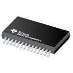
| 供应商器件封装 | 28-SSOP |
| 关闭 | Yes |
| 其它名称 | 296-26162-5 |
| 功能 | Transceiver |
| 包装 | 管件 |
| 协议 | RS232 |
| 单位重量 | 208.400 mg |
| 双工 | 全 |
| 商标 | Texas Instruments |
| 安装类型 | 表面贴装 |
| 安装风格 | SMD/SMT |
| 封装 | Tube |
| 封装/外壳 | 28-SSOP(0.209",5.30mm 宽) |
| 封装/箱体 | SSOP-28 |
| 工作温度 | 0°C ~ 70°C |
| 工作温度范围 | 0 C to + 70 C |
| 工作电源电压 | 3.3 V, 5 V |
| 工厂包装数量 | 50 |
| 接收器滞后 | 300mV |
| 接收机数量 | 5 Receiver |
| 数据速率 | 250kbps |
| 最大工作温度 | + 70 C |
| 最小工作温度 | 0 C |
| 标准包装 | 50 |
| 激励器数量 | 3 Driver |
| 电压-电源 | 3 V ~ 5.5 V |
| 电源电流 | 1 mA |
| 类型 | 收发器 |
| 系列 | MAX3243 |
| 输入/输出端数量 | 16 |
| 驱动器/接收器数 | 3/5 |


- 商务部:美国ITC正式对集成电路等产品启动337调查
- 曝三星4nm工艺存在良率问题 高通将骁龙8 Gen1或转产台积电
- 太阳诱电将投资9.5亿元在常州建新厂生产MLCC 预计2023年完工
- 英特尔发布欧洲新工厂建设计划 深化IDM 2.0 战略
- 台积电先进制程称霸业界 有大客户加持明年业绩稳了
- 达到5530亿美元!SIA预计今年全球半导体销售额将创下新高
- 英特尔拟将自动驾驶子公司Mobileye上市 估值或超500亿美元
- 三星加码芯片和SET,合并消费电子和移动部门,撤换高东真等 CEO
- 三星电子宣布重大人事变动 还合并消费电子和移动部门
- 海关总署:前11个月进口集成电路产品价值2.52万亿元 增长14.8%


PDF Datasheet 数据手册内容提取
Product Sample & Technical Tools & Support & Folder Buy Documents Software Community MAX3243 SLLS350O–APRIL1999–REVISEDJANUARY2015 MAX3243 3-V to 5.5-V Multichannel RS-232 Line Driver/Receiver With ±15-kV ESD (HBM) Protection 1 Features 2 Applications • OperatesWith3-Vto5.5-VV Supply • Battery-PoweredSystems 1 CC • Single-ChipandSingle-SupplyInterface • Tablets forIBM™PC/AT™SerialPort • Notebooks • RS-232Bus-PinESDProtectionof • Laptops ±15kVUsingHuman-BodyModel(HBM) • Hand-HeldEquipment • MeetsorExceedstheRequirementsof TIA/EIA-232-FandITUV.28Standards 3 Description • ThreeDriversandFiveReceivers The MAX3243 device consists of three line drivers, • OperatesUpTo250kbit/s five line receivers which is ideal for DE-9 DTE interface. ±15-kV ESD (HBM) protection pin to pin • LowActiveCurrent:300μATypical (serial- port connection pins, including GND). Flexible • LowStandbyCurrent:1 μATypical power features saves power automatically. Special • ExternalCapacitors:4 ×0.1 μF outputs ROUT2B and INVALID are always enabled to allow checking for ring indicator and valid RS232 • Accepts5-VLogicInputWith3.3-VSupply input. • Always-ActiveNoninvertingReceiver Output(ROUT2B) DeviceInformation(1) • OperatingTemperature PARTNUMBER PACKAGE(PIN) BODYSIZE – MAX3243C:0°Cto70°C SSOP(28) 10.29mm×5.30mm – MAX3243I: –40°Cto85°C MAX3243 SOIC(28) 17.90mm×7.50mm • Serial-MouseDriveability TSSOP(28) 9.70mm×4.40mm • Auto-PowerdownFeaturetoDisableDriver (1) For all available packages, see the orderable addendum at OutputsWhenNoValidRS-232SignalIs theendofthedatasheet. Sensed 4 Simplified Diagram 3.3 V, 5 V FORCEON POWER FORCEOFF 3 3 DOUT DIN TX RS232 5 5 RIN ROUT RX RS232 INVALID STATUS 1 An IMPORTANT NOTICE at the end of this data sheet addresses availability, warranty, changes, use in safety-critical applications, intellectualpropertymattersandotherimportantdisclaimers.PRODUCTIONDATA.
MAX3243 SLLS350O–APRIL1999–REVISEDJANUARY2015 www.ti.com Table of Contents 1 Features.................................................................. 1 8 ParameterMeasurementInformation..................8 2 Applications........................................................... 1 9 DetailedDescription............................................ 11 3 Description............................................................. 1 9.1 Overview.................................................................11 4 SimplifiedDiagram................................................ 1 9.2 FunctionalBlockDiagram.......................................11 5 RevisionHistory..................................................... 2 9.3 FeatureDescription.................................................12 9.4 DeviceFunctionalModes........................................13 6 PinConfigurationandFunctions......................... 3 10 ApplicationandImplementation........................ 14 7 Specifications......................................................... 4 10.1 ApplicationInformation..........................................14 7.1 AbsoluteMaximumRatings .....................................4 10.2 TypicalApplication................................................14 7.2 ESDRatings..............................................................4 11 PowerSupplyRecommendations..................... 16 7.3 RecommendedOperatingConditions.......................4 7.4 ThermalInformation..................................................4 12 Layout................................................................... 16 7.5 ElectricalCharacteristics––AutoPowerDown........5 12.1 LayoutGuidelines.................................................16 7.6 ElectricalCharacteristics––Driver ..........................5 12.2 LayoutExample....................................................17 7.7 ElectricalCharacteristics––Receiver .....................6 13 DeviceandDocumentationSupport................. 18 7.8 SwitchingCharacteristics––AutoPowerDown ......6 13.1 Trademarks...........................................................18 7.9 SwitchingCharacteristics––Driver .........................6 13.2 ElectrostaticDischargeCaution............................18 7.10 SwitchingCharacteristics––Receiver...................6 13.3 Glossary................................................................18 7.11 TypicalCharacteristics............................................7 14 Mechanical,Packaging,andOrderable Information........................................................... 18 5 Revision History ChangesfromRevisionN(May2009)toRevisionO Page • AddedApplications,DeviceInformationtable,PinFunctionstable,ESDRatingstable,ThermalInformationtable, TypicalCharacteristics,FeatureDescriptionsection,DeviceFunctionalModes,ApplicationandImplementation section,PowerSupplyRecommendationssection,Layoutsection,DeviceandDocumentationSupportsection,and Mechanical,Packaging,andOrderableInformationsection.................................................................................................. 1 • DeletedOrderingInformationtable........................................................................................................................................ 1 2 SubmitDocumentationFeedback Copyright©1999–2015,TexasInstrumentsIncorporated ProductFolderLinks:MAX3243
MAX3243 www.ti.com SLLS350O–APRIL1999–REVISEDJANUARY2015 6 Pin Configuration and Functions DB, DW, OR PW PACKAGE (TOPVIEW) C2+ 1 28 C1+ C2− 2 27 V+ V− 3 26 VCC RIN1 4 25 GND RIN2 5 24 C1− RIN3 6 23 FORCEON RIN4 7 22 FORCEOFF RIN5 8 21 INVALID DOUT1 9 20 ROUT2B DOUT2 10 19 ROUT1 DOUT3 11 18 ROUT2 DIN3 12 17 ROUT3 DIN2 13 16 ROUT4 DIN1 14 15 ROUT5 PinFunctions PIN TYPE DESCRIPTION NAME NO. C2+ 1 — PositiveleadofC2capacitor C2– 2 — NegativeleadofC2capacitor V– 3 O Negativechargepumpoutputforstoragecapacitoronly RIN1:RIN5 4,5,6,7,8 I RS232linedatainput(fromremoteRS232system) DOUT1:DOUT3 9,10,11 O RS232linedataoutput(toremoteRS232system) DIN3:DIN1 12,13,14 I Logicdatainput(fromUART) ROUT5:ROUT1 15,16,17,18,19 O Logicdataoutput(toUART) AlwaysActivenon-invertingoutputforRIN2(normallyusedforring ROUT2B 20 O indicator) INVALID 21 O ActivelowoutputwhenallRINareunpowered LowinputforcesDOUT1-5,ROUT1-5highZperDeviceFunctional FORCEOFF 22 I Modes Highforcesdriverson.LowisautomaticmodeperDeviceFunctional FORCEON 23 I Modes C1– 24 — NegativeleadonC1capacitor GND 25 — Ground V 26 — SupplyVoltage,Connectto3Vto5.5Vpowersupply CC V+ 27 O Positivechargepumpoutputforstoragecapacitoronly C1+ 28 — PositiveleadofC1capacitor Copyright©1999–2015,TexasInstrumentsIncorporated SubmitDocumentationFeedback 3 ProductFolderLinks:MAX3243
MAX3243 SLLS350O–APRIL1999–REVISEDJANUARY2015 www.ti.com 7 Specifications 7.1 Absolute Maximum Ratings overoperatingfree-airtemperaturerange(unlessotherwisenoted) (1) MIN MAX UNIT V Supplyvoltagerange(2) –0.3 6 V CC V+ Positiveoutputsupplyvoltagerange(2) –0.3 7 V V– Negativeoutputsupplyvoltagerange(2) 0.3 –7 V V+–V– Supplyvoltagedifference(2) 13 V Driver,FORCEOFF,FORCEON –0.3 6 V Inputvoltagerange V I Receiver –25 25 Driver –13.2 13.2 V Outputvoltagerange V O Receiver,INVALID –0.3 V +0.3 CC T Operatingvirtualjunctiontemperature 150 °C J T Storagetemperaturerange –65 150 °C stg (1) StressesbeyondthoselistedunderAbsoluteMaximumRatingsmaycausepermanentdamagetothedevice.Thesearestressratings only,andfunctionaloperationofthedeviceattheseoranyotherconditionsbeyondthoseindicatedunderRecommendedOperating Conditionsisnotimplied.Exposuretoabsolute-maximum-ratedconditionsforextendedperiodsmayaffectdevicereliability. (2) AllvoltagesarewithrespecttonetworkGND. 7.2 ESD Ratings MAX UNIT Humanbodymodel(HBM),perANSI/ESDA/JEDECJS-001 RIN,DOUT,andGNDpins (1) 15000 Humanbodymodel(HBM),perANSI/ESDA/JEDECJS-001 V(ESD) Electrostaticdischarge Allotherpins(1) 3000 V Chargeddevicemodel(CDM),perJEDECspecificationJESD22-C101, allpins(2) 1000 (1) JEDECdocumentJEP155statesthat500-VHBMallowssafemanufacturingwithastandardESDcontrolprocess. (2) JEDECdocumentJEP157statesthat250-VCDMallowssafemanufacturingwithastandardESDcontrolprocess. 7.3 Recommended Operating Conditions (1)(SeeFigure8) MIN NOM MAX UNIT V =3.3V 3 3.3 3.6 CC V Supplyvoltage V CC V =5V 4.5 5 5.5 CC DIN,FORCEOFF, VCC=3.3V 2 5.5 V Driverandcontrolhigh-levelinputvoltage V IH FORCEON V =5V 2.4 5.5 CC V Driverandcontrollow-levelinputvoltage DIN,FORCEOFF,FORCEON 0 0.8 V IL V Driverandcontrolinputvoltage DIN,FORCEOFF,FORCEON 0 5.5 V I V Receiverinputvoltage –25 25 V I MAX3243C 0 70 T Operatingfree-airtemperature °C A MAX3243I –40 85 (1) TestconditionsareC1–C4=0.1μFatV =3.3V±0.3V;C1=0.047μF,C2–C4=0.33μFatV =5V±0.5V. CC CC 7.4 Thermal Information MAX3243 THERMALMETRIC(1) DB DW PW UNIT 16PINS 16PINS 16PINS R Junction-to-ambientthermalresistance 62 46 62 °C/W θJA (1) Formoreinformationabouttraditionalandnewthermalmetrics,seetheICPackageThermalMetricsapplicationreport(SPRA953). 4 SubmitDocumentationFeedback Copyright©1999–2015,TexasInstrumentsIncorporated ProductFolderLinks:MAX3243
MAX3243 www.ti.com SLLS350O–APRIL1999–REVISEDJANUARY2015 7.5 Electrical Characteristics –– Auto Power Down overrecommendedrangesofsupplyvoltageandoperatingfree-airtemperature(unlessotherwisenoted)(1)(seeFigure8) PARAMETER TESTCONDITIONS MIN TYP(2) MAX UNIT Supplycurrent Auto-powerdown Noload,FORCEOFFandFORCEONatV .T =25°C 0.3 1 mA CC A disabled Supplycurrent I Noload,FORCEOFFatGND.T =25°C 1 10 CC Poweredoff A Supplycurrent Noload,FORCEOFFatV ,FORCEONatGND, μA CC Auto-powerdown AllRINareopenorgrounded,AllDINaregrounded.T = 1 10 A enabled 25°C I Inputleakagecurrent I V =V orV atGND ±0.01 ±1 μA ofFORCEOFF,FORCEON I CC I Receiverinputthreshold FORCEON=GND, V forINVALIDhigh-leveloutput 2.7 V IT+ FORCEOFF=V voltage CC Receiverinputthreshold FORCEON=GND, V forINVALIDhigh-leveloutput –2.7 V IT– FORCEOFF=V voltage CC Receiverinputthreshold FORCEON=GND, V forINVALIDlow-leveloutput –0.3 0.3 V T FORCEOFF=V voltage CC INVALIDhigh-leveloutput I =-1mA,FORCEON=GND, V OH V –0.6 V OH voltage FORCEOFF=V CC CC INVALIDlow-leveloutput I =1.6mA,FORCEON=GND, V OL 0.4 V OL voltage FORCEOFF=V CC (1) TestconditionsareC1–C4=0.1μFatV =3.3V±0.3V;C1=0.047μF,C2–C4=0.33μFatV =5V±0.5V. CC CC (2) StressesbeyondthoselistedunderAbsoluteMaximumRatingsmaycausepermanentdamagetothedevice.Thesearestressratings only,andfunctionaloperationofthedeviceattheseoranyotherconditionsbeyondthoseindicatedunderRecommendedOperating Conditionsisnotimplied.Exposuretoabsolute-maximum-ratedconditionsforextendedperiodsmayaffectdevicereliability. 7.6 Electrical Characteristics –– Driver overrecommendedrangesofsupplyvoltageandoperatingfree-airtemperature(unlessotherwisenoted)(1)(seeFigure8) PARAMETER TESTCONDITIONS MIN TYP(2) MAX UNIT V High-leveloutputvoltage AllDOUTatR =3kΩtoGND 5 5.4 V OH L V Low-leveloutputvoltage AllDOUTatR =3kΩtoGND –5 –5.4 V OL L Outputvoltage DIN1=DIN2=GND,DIN3=V ,3-kΩtoGNDatDOUT3, V CC ±5 V O (mousedriveability) DOUT1=DOUT2=2.5mA I High-levelinputcurrent V =V ±0.01 ±1 μA IH I CC I Low-levelinputcurrent V atGND ±0.01 ±1 μA IL I V Inputhysteresis ±1 V hys V =3.6V, V =0V I Short-circuitoutputcurrent(3) CC O ±35 ±60 mA OS V =5.5V, V =0V CC O r Outputresistance V ,V+,andV–=0V, V =±2V 300 10M Ω o CC O V =±12V, V =3to3.6V ±25 O CC I Outputleakagecurrent FORCEOFF=GND, μA off V =±10V, V =4.5to5.5V ±25 O CC (1) TestconditionsareC1–C4=0.1μFatV =3.3V±0.3V;C1=0.047μF,C2–C4=0.33μFatV =5V±0.5V. CC CC (2) AlltypicalvaluesareatV =3.3VorV =5V,andT =25°C. CC CC A (3) Short-circuitdurationsshouldbecontrolledtopreventexceedingthedeviceabsolutepowerdissipationratings,andnotmorethanone outputshouldbeshortedatatime. Copyright©1999–2015,TexasInstrumentsIncorporated SubmitDocumentationFeedback 5 ProductFolderLinks:MAX3243
MAX3243 SLLS350O–APRIL1999–REVISEDJANUARY2015 www.ti.com 7.7 Electrical Characteristics –– Receiver overrecommendedrangesofsupplyvoltageandoperatingfree-airtemperature(unlessotherwisenoted)(1)(seeFigure8) PARAMETER TESTCONDITIONS MIN TYP(2) MAX UNIT V High-leveloutputvoltage I =–1mA V –0.6 V –0.1 V OH OH CC CC V Low-leveloutputvoltage I =1.6mA 0.4 V OL OH V =3.3V 1.6 2.4 CC V Positive-goinginputthresholdvoltage V IT+ V =5V 1.9 2.4 CC V =3.3V 0.6 1.1 CC V Negative-goinginputthresholdvoltage V IT– V =5V 0.8 1.4 CC V Inputhysteresis(V –V ) 0.5 V hys IT+ IT– I Outputleakagecurrent(exceptROUT2B) FORCEOFF=0V ±0.05 ±10 μA off r Inputresistance V =±3Vor±25V 3 5 7 kΩ I I (1) TestconditionsareC1–C4=0.1μFatV =3.3V±0.3V;C1=0.047μF,C2–C4=0.33μFatV =5V±0.5V. CC CC (2) AlltypicalvaluesareatV =3.3VorV =5V,andT =25°C. CC CC A 7.8 Switching Characteristics –– Auto Power Down overrecommendedrangesofsupplyvoltageandoperatingfree-airtemperature(unlessotherwisenoted)(seeFigure7) PARAMETER TESTCONDITIONS TYP(1) UNIT t Propagationdelaytime,low-tohigh-leveloutput V =5V 1 μs valid CC t Propagationdelaytime,high-tolow-leveloutput V =5V 30 μs invalid CC t Supplyenabletime V =5V 100 μs en CC (1) AlltypicalvaluesareatV =3.3VorV =5V,andT =25°C. CC CC A 7.9 Switching Characteristics –– Driver overrecommendedrangesofsupplyvoltageandoperatingfree-airtemperature(unlessotherwisenoted)(1)(seeFigure8) MAX3243C,MAX3243I PARAMETER TESTCONDITIONS MIN TYP(2) MAX UNIT R =3kΩ C =1000pF Maximumdatarate L L 150 250 kbit/s OneDOUTswitching, SeeFigure3 t Pulseskew(3) R =3kΩto7kΩ CL=150pFto2500pF 100 ns sk(p) L SeeFigure5 SR(tr) Slewrate,transitionregion VCC=3.3V, CL=150pFto1000pF 6 30 V/μs (seeFigure3) RL=3kΩto7kΩ CL=150pFto2500pF 4 30 (1) TestconditionsareC1–C4=0.1μFatV =3.3V+0.3V;C1=0.047μF,C2–C4=0.33μFatV =5V±0.5V. CC CC (2) AlltypicalvaluesareatV =3.3VorV =5V,andT =25°C. CC CC A (3) Pulseskewisdefinedas|t –t |ofeachchannelofthesamedevice. PLH PHL 7.10 Switching Characteristics –– Receiver overrecommendedrangesofsupplyvoltageandoperatingfree-airtemperature(unlessotherwisenoted)(1) PARAMETER TESTCONDITIONS TYP(2) UNIT tPLH Propagationdelaytime,low-tohigh-leveloutput CL=150pF, 150 ns t Propagationdelaytime,high-tolow-leveloutput SeeFigure5 150 ns PHL ten Outputenabletime CL=150pF,RL=3kΩ, 200 ns t Outputdisabletime SeeFigure6 200 ns dis t Pulseskew(3) SeeFigure5 50 ns sk(p) (1) TestconditionsareC1–C4=0.1μFatV =3.3V±0.3V;C1=0.047μF,C2–C4=0.33μFatV =5V±0.5V. CC CC (2) AlltypicalvaluesareatV =3.3VorV =5V,andT =25°C. CC CC A (3) Pulseskewisdefinedas|t -t |ofeachchannelofthesamedevice. PLH PHL 6 SubmitDocumentationFeedback Copyright©1999–2015,TexasInstrumentsIncorporated ProductFolderLinks:MAX3243
MAX3243 www.ti.com SLLS350O–APRIL1999–REVISEDJANUARY2015 7.11 Typical Characteristics V =3.3V CC 6 0 VOH 5 ±1 4 ±2 V) V) (OH3 (OL±3 V V 2 ±4 1 ±5 VOL 0 ±6 0 5 10 15 20 25 30 35 0 5 10 15 20 25 30 35 Load Current (mA) Load Current (mA) C001 C001 Figure1.DOUTVOHvsLoadCurrent Figure2.DOUTVOLvsLoadCurrent Copyright©1999–2015,TexasInstrumentsIncorporated SubmitDocumentationFeedback 7 ProductFolderLinks:MAX3243
MAX3243 SLLS350O–APRIL1999–REVISEDJANUARY2015 www.ti.com 8 Parameter Measurement Information 3 V RS-232 Input Output 0 V Generator 50W (see Note B) RL C(sLee NoteA) tTHL tTLH 3 V 3 V 3 V VOH Output FORCEOFF −3 V −3 V VOL 6V SR(tr) t ort TEST CIRCUIT THL TLH VOLTAGE WAVEFORMS NOTES: A. CLincludes probe and jig capacitance. B. Thepulsegeneratorhasthefollowingcharacteristics:PRR=250kbit/s(MAX3243C/I)and1Mbit/s(MAX3243FC/I), ZO= 50W, 50% duty cycle, tr≤10 ns, tf≤10 ns. Figure3.DriverSlewRate 3 V RS-232 Input 1.5 V 1.5 V Output 0 V Generator 50W (see Note B) RL C(sLee NoteA) tPHL tPLH VOH 3 V Output 50% 50% FORCEOFF VOL TEST CIRCUIT VOLTAGE WAVEFORMS NOTES: A. CLincludes probe and jig capacitance. B. Thepulsegeneratorhasthefollowingcharacteristics:PRR=250kbit/s(MAX3243C/I)and1Mbit/s(MAX3243FC/I), ZO= 50W, 50% duty cycle, tr≤10 ns, tf≤10 ns. Figure4.DriverPulseSkew 3 V or 0 V 3 V FORCEON Input 1.5 V 1.5 V −3 V Output Generator 50W tPHL tPLH (see Note B) CL (see NoteA) 3 V VOH FORCEOFF Output 50% 50% VOL TEST CIRCUIT VOLTAGE WAVEFORMS NOTES: A. CLincludes probe and jig capacitance. B. The pulse generator has the following characteristics: ZO= 50W, 50% duty cycle, tr≤10 ns, tf≤10 ns. Figure5.ReceiverPropagationDelayTimes 8 SubmitDocumentationFeedback Copyright©1999–2015,TexasInstrumentsIncorporated ProductFolderLinks:MAX3243
MAX3243 www.ti.com SLLS350O–APRIL1999–REVISEDJANUARY2015 Parameter Measurement Information (continued) 3 V Input VCC GND 1.5 V 1.5 V 3 V or 0 V 0 V S1 FORCEON tPHZ tPZH RL (S1 at GND) (S1 at GND) 3 V or 0 V Output VOH Output 50% CL 0.3 V FORCEOFF (see NoteA) tPLZ tPZL Generator (S1 at VCC) (S1 at VCC) 50W (see Note B) 0.3 V Output 50% VOL TEST CIRCUIT VOLTAGE WAVEFORMS NOTES: A. CLincludes probe and jig capacitance. B. The pulse generator has the following characteristics: ZO= 50W, 50% duty cycle, tr≤10 ns, tf≤10 ns. C. tPLZand tPHZare the same as tdis. D. tPZLand tPZHare the same as ten. Figure6.ReceiverEnableandDisableTimes Copyright©1999–2015,TexasInstrumentsIncorporated SubmitDocumentationFeedback 9 ProductFolderLinks:MAX3243
MAX3243 SLLS350O–APRIL1999–REVISEDJANUARY2015 www.ti.com Parameter Measurement Information (continued) 3 V 2.7 V 2.7 V Receiver 0 V Input 0 V ROUT −2.7 V −2.7 V −3 V Generator 50W (see Note B) tinvalid tvalid VCC 50% VCC 50% VCC INVALID 0 V Output Auto- INVALID ten powerdown V+ ≈V+ CL= 30 pF (see NoteA) 0.3 V Supply VCC FORCEOFF Voltages 0 V 0.3 V DIN DOUT FORCEON V− ≈V− TEST CIRCUIT VOLTAGE WAVEFORMS Valid RS-232 Level, INVALIDHigh 2.7 V Indeterminate 0.3 V If Signal Remains Within This Region 0 V For More Than 30ms, INVALIDIs Low (see Note C) −0.3 V Indeterminate −2.7 V Valid RS-232 Level, INVALIDHigh NOTES: A. CLincludes probe and jig capacitance. B. The pulse generator has the following characteristics: PRR = 5 kbit/s, ZO= 50W, 50% duty cycle, tr≤10 ns, tf≤10 ns. C. Auto-powerdown disables drivers and reduces supply current to 1mA. Figure7. INVALID PropagationDelayTimesandSupplyEnablingTime 10 SubmitDocumentationFeedback Copyright©1999–2015,TexasInstrumentsIncorporated ProductFolderLinks:MAX3243
MAX3243 www.ti.com SLLS350O–APRIL1999–REVISEDJANUARY2015 9 Detailed Description 9.1 Overview The MAX3243 device consists of three line drivers, five line receivers, and a dual charge-pump circuit with ±15- kV ESD (HBM) protection pin to pin (serial- port connection pins, including GND). The device meets the requirements of TIA/EIA-232-F and provides the electrical interface between an asynchronous communication controller and the serial-port connector. This combination of drivers and receivers matches that needed for the typical serial port used in an IBM PC/AT, or compatible. The charge pump and four small external capacitors allow operation from a single 3-V to 5.5-V supply. In addition, the device includes an always-active noninverting output (ROUT2B), which allows applications using the ring indicator to transmit data while the device is powered down. Flexible control options for power management are available. when the serial port is inactive. The auto- power-down feature functions when FORCEON is low and FORCEOFF is high. During this mode of operation, if the device does not sense a valid RS-232 signal, the driver outputs are disabled. If FORCEOFF is set low, both drivers and receivers (except ROUT2B) are shut off, and the supply current is reduced to 1 µA. Disconnecting the serial port or turning off the peripheral drivers causes the auto-powerdown condition to occur. Auto- powerdown can be disabled when FORCEON and FORCEOFF are high and should be done when driving a serial mouse. With auto-powerdown enabled, the device is activated automatically when a valid signal is applied toanyreceiverinput.TheINVALIDoutputisusedtonotifytheuserifanRS-232signalispresentatanyreceiver input. INVALID is high (valid data) if any receiver input voltage is greater than 2.7 V or less than –2.7 V or has beenbetween–0.3Vand0.3Vforlessthan30 µs.INVALIDislow(invaliddata)ifallreceiverinputvoltagesare between –0.3Vand0.3Vformorethan30 µs. 9.2 Functional Block Diagram 14 9 DIN1 DOUT1 13 10 DIN2 DOUT2 12 11 DIN3 DOUT3 22 FORCEOFF 21 Auto-powerdown INVALID 23 FORCEON 19 4 ROUT1 RIN1 ROUT2B 20 5 kW 18 5 ROUT2 RIN2 5 kW 17 6 ROUT3 RIN3 5 kW 16 7 ROUT4 RIN4 5 kW 15 8 ROUT5 RIN5 5 kW Copyright©1999–2015,TexasInstrumentsIncorporated SubmitDocumentationFeedback 11 ProductFolderLinks:MAX3243
MAX3243 SLLS350O–APRIL1999–REVISEDJANUARY2015 www.ti.com 9.3 Feature Description 9.3.1 Auto-Power-Down Auto-Power-Downcanbeusedtoautomaticallysavepowerwhenthereceiversareunconnectedorconnectedto a powered down remote RS232 port. FORCEON being high will override Auto power down and the drivers will be active. FORCEOFF being low will override FORCEON and will power down all outputs except for ROUT2B andINVALID. 9.3.2 ChargePump The charge pump increases, inverts, and regulates voltage at V+ and V– pins and requires four external capacitors. 9.3.3 RS232Driver ThreedriversinterfacestandardlogicleveltoRS232levels.AllDINinputsmustbevalidhighorlow. 9.3.4 RS232Receiver FivereceiversinterfaceRS232levelstostandardlogiclevels.AnopeninputwillresultinahighoutputonROUT. EachRINinputincludesaninternalstandardRS232load. 9.3.5 ROUT2BReceiver ROUT2B is an always-active noninverting output of RIN2 input, which allows applications using the ring indicator totransmitdatawhilethedeviceispowereddown. 9.3.6 InvalidInputDetection The INVALID output goes active low when all RIN inputs are unpowered. The INVALID output goes inactive high whenanyRINinputisconnectedtoanactiveRS232voltagelevel. 12 SubmitDocumentationFeedback Copyright©1999–2015,TexasInstrumentsIncorporated ProductFolderLinks:MAX3243
MAX3243 www.ti.com SLLS350O–APRIL1999–REVISEDJANUARY2015 9.4 Device Functional Modes Table1.EachDriver(1) INPUTS OUTPUT VALIDRIN DRIVERSTATUS DIN FORCEON FORCEOFF DOUT RS-232LEVEL X X L X Z Poweredoff L H H X H Normaloperationwith H H H X L auto-powerdowndisabled L L H YES H Normaloperationwith H L H YES L auto-powerdownenabled Poweroffby X L H NO Z auto-powerdownfeature (1) H=highlevel,L=lowlevel,X=irrelevant,Z=highimpedance,YES=anyRINvalid,NO=allRINinvalid Table2.EachReceiver(1) INPUTS OUTPUTS RECEIVERSTATUS RIN FORCEON FORCEOFF ROUT X X L Z Poweredoff L X H H H X H L Normaloperation Open X H H (1) H=highlevel,L=lowlevel,X=irrelevant,Z=highimpedance(off),Open=inputdisconnectedorconnecteddriveroff Table3.INVALID andROUT2BOutputs(1) INPUTS OUTPUTS VALIDRIN OUTPUTSTATUS RS-232 RIN2 FORCEON FORCEOFF INVALID ROUT2B LEVEL YES L X X H L AlwaysActive YES H X X H H YES OPEN X X H L AlwaysActive NO OPEN X X L L (1) H=highlevel,L=lowlevel,X=irrelevant,Z=highimpedance(off), OPEN=inputdisconnectedorconnecteddriveroff,YES=anyRINvalid,NO=allRINinvalid Copyright©1999–2015,TexasInstrumentsIncorporated SubmitDocumentationFeedback 13 ProductFolderLinks:MAX3243
MAX3243 SLLS350O–APRIL1999–REVISEDJANUARY2015 www.ti.com 10 Application and Implementation NOTE Information in the following applications sections is not part of the TI component specification, and TI does not warrant its accuracy or completeness. TI’s customers are responsible for determining suitability of components for their purposes. Customers should validateandtesttheirdesignimplementationtoconfirmsystemfunctionality. 10.1 Application Information ItisrecommendedtoaddcapacitorsasshowninFigure8. 10.2 Typical Application ROUT and DIN connect to UART or general purpose logic lines. RIN and DOUT lines connect to a RS232 connectororcable. 28 C1+ 27 1 V+ C2+− 2 CC22+− VCC 26 + CBY+−PASCS3(1) +− C1 3 V− 25 − = 0.1mF − GND C4 + 24 C1− 4 23 RIN1 FORCEON 5 RIN2 n RS-232 Inputs RIN3 67 Auto-werdow 22 FORCEOFF RIN4 o p 8 RIN5 21 INVALID 9 20 DOUT1 ROUT2B 10 19 RS-232 Outputs DOUT2 ROUT1 5 kW 11 18 DOUT3 ROUT2 5 kW Logic Outputs 12 17 DIN3 ROUT3 5 kW Logic Inputs DIN2 13 16 ROUT4 5 kW 14 15 DIN1 ROUT5 5 kW (1) C3 can be connected to VCCor GND. VCCvs CAPACITOR VALUES NOTES: A. Resistor values shown are nominal. VCC C1 C2, C3, and C4 B. Nonpolarizedceramic capacitors are acceptable. If polarized tantalum orelectrolyticcapacitorsareused,theyshouldbeconnectedas 3.3 V±0.3 V 0.1mF 0.1mF shown. 5 V±0.5 V 0.047mF 0.33mF 3 V to 5.5 V 0.1mF 0.47mF Figure8. TypicalOperatingCircuitandCapacitorValues 14 SubmitDocumentationFeedback Copyright©1999–2015,TexasInstrumentsIncorporated ProductFolderLinks:MAX3243
MAX3243 www.ti.com SLLS350O–APRIL1999–REVISEDJANUARY2015 Typical Application (continued) 10.2.1 DesignRequirements • V minimumis3Vandmaximumis5.5V. CC • Maximumrecommendedbitrateis250kbit/s. 10.2.2 DetailedDesignProcedure • AllDIN, FORCEOFF andFORCEONinputsmustbeconnectedtovalidloworhighlogiclevels. • SelectcapacitorvaluesbasedonV levelforbestperformance. CC 10.2.3 ApplicationCurves V =3.3V CC 6 5 4 3 2 1 V) 0 e (±1 ag±2 olt±3 V ±4 ±5 ±6 ±7 DIN ±8 DOUT to RIN ±9 ROUT 0 1 2 3 4 5 6 7 Time ((cid:29)s) C001 Figure9.DrivertoReceiverLoopbackTimingWaveform Copyright©1999–2015,TexasInstrumentsIncorporated SubmitDocumentationFeedback 15 ProductFolderLinks:MAX3243
MAX3243 SLLS350O–APRIL1999–REVISEDJANUARY2015 www.ti.com 11 Power Supply Recommendations V shouldbebetween3Vand5.5V.ChargepumpcapacitorsshouldbechosenusingtableinFigure8. CC 12 Layout 12.1 Layout Guidelines Keep the external capacitor traces short. This is more important on C1 and C2 nodes that have the fastest rise andfalltimes. In the Layout Example diagram, only critical layout sections are shown. Input and output traces will vary in shape and size depending on the customer application. FORCEON and /FORCEOFF should be pulled up to VCC or GNDviaapullupresistor,dependingonwhichconfigurationtheuserdesiresuponpower-up. 16 SubmitDocumentationFeedback Copyright©1999–2015,TexasInstrumentsIncorporated ProductFolderLinks:MAX3243
MAX3243 www.ti.com SLLS350O–APRIL1999–REVISEDJANUARY2015 12.2 Layout Example C1 1 C2+ C1+ 28 C2 2 C2- V+ 27 Ground C3 Ground 3 V- VCC 26 VCC C4 0.1μF 4 RIN1 GND 25 Ground 5 RIN2 C1- 24 6 RIN3 FORCEON 23 7 RIN4 FORCEOFF 22 8 RIN5 INVALID 21 9 DOUT1 ROUT2B 20 10 DOUT2 ROUT1 19 11 DOUT3 ROUT2 18 12 DIN3 ROUT3 17 13 DIN2 ROUT4 16 14 DIN1 ROUT5 15 Figure10. LayoutDiagram Copyright©1999–2015,TexasInstrumentsIncorporated SubmitDocumentationFeedback 17 ProductFolderLinks:MAX3243
MAX3243 SLLS350O–APRIL1999–REVISEDJANUARY2015 www.ti.com 13 Device and Documentation Support 13.1 Trademarks IBM,PC/ATaretrademarksofIBM. Allothertrademarksarethepropertyoftheirrespectiveowners. 13.2 Electrostatic Discharge Caution Thesedeviceshavelimitedbuilt-inESDprotection.Theleadsshouldbeshortedtogetherorthedeviceplacedinconductivefoam duringstorageorhandlingtopreventelectrostaticdamagetotheMOSgates. 13.3 Glossary SLYZ022—TIGlossary. Thisglossarylistsandexplainsterms,acronyms,anddefinitions. 14 Mechanical, Packaging, and Orderable Information The following pages include mechanical, packaging, and orderable information. This information is the most current data available for the designated devices. This data is subject to change without notice and revision of thisdocument.Forbrowser-basedversionsofthisdatasheet,refertotheleft-handnavigation. 18 SubmitDocumentationFeedback Copyright©1999–2015,TexasInstrumentsIncorporated ProductFolderLinks:MAX3243
PACKAGE OPTION ADDENDUM www.ti.com 6-Feb-2020 PACKAGING INFORMATION Orderable Device Status Package Type Package Pins Package Eco Plan Lead/Ball Finish MSL Peak Temp Op Temp (°C) Device Marking Samples (1) Drawing Qty (2) (6) (3) (4/5) MAX3243CDB ACTIVE SSOP DB 28 50 Green (RoHS NIPDAU Level-1-260C-UNLIM 0 to 70 MAX3243C & no Sb/Br) MAX3243CDBG4 ACTIVE SSOP DB 28 50 Green (RoHS NIPDAU Level-1-260C-UNLIM 0 to 70 MAX3243C & no Sb/Br) MAX3243CDBR ACTIVE SSOP DB 28 2000 Green (RoHS NIPDAU Level-1-260C-UNLIM 0 to 70 MAX3243C & no Sb/Br) MAX3243CDBRE4 ACTIVE SSOP DB 28 2000 Green (RoHS NIPDAU Level-1-260C-UNLIM 0 to 70 MAX3243C & no Sb/Br) MAX3243CDBRG4 ACTIVE SSOP DB 28 2000 Green (RoHS NIPDAU Level-1-260C-UNLIM 0 to 70 MAX3243C & no Sb/Br) MAX3243CDW ACTIVE SOIC DW 28 20 Green (RoHS NIPDAU Level-1-260C-UNLIM 0 to 70 MAX3243C & no Sb/Br) MAX3243CDWE4 ACTIVE SOIC DW 28 20 Green (RoHS NIPDAU Level-1-260C-UNLIM 0 to 70 MAX3243C & no Sb/Br) MAX3243CDWR ACTIVE SOIC DW 28 1000 Green (RoHS NIPDAU Level-1-260C-UNLIM 0 to 70 MAX3243C & no Sb/Br) MAX3243CDWRG4 ACTIVE SOIC DW 28 1000 Green (RoHS NIPDAU Level-1-260C-UNLIM 0 to 70 MAX3243C & no Sb/Br) MAX3243CPW ACTIVE TSSOP PW 28 50 Green (RoHS NIPDAU Level-1-260C-UNLIM 0 to 70 MA3243C & no Sb/Br) MAX3243CPWE4 ACTIVE TSSOP PW 28 50 Green (RoHS NIPDAU Level-1-260C-UNLIM 0 to 70 MA3243C & no Sb/Br) MAX3243CPWR ACTIVE TSSOP PW 28 2000 Green (RoHS NIPDAU Level-1-260C-UNLIM 0 to 70 MA3243C & no Sb/Br) MAX3243CPWRG4 ACTIVE TSSOP PW 28 2000 Green (RoHS NIPDAU Level-1-260C-UNLIM 0 to 70 MA3243C & no Sb/Br) MAX3243IDB ACTIVE SSOP DB 28 50 Green (RoHS NIPDAU Level-1-260C-UNLIM -40 to 85 MAX3243I & no Sb/Br) MAX3243IDBG4 ACTIVE SSOP DB 28 50 Green (RoHS NIPDAU Level-1-260C-UNLIM -40 to 85 MAX3243I & no Sb/Br) MAX3243IDBR ACTIVE SSOP DB 28 2000 Green (RoHS NIPDAU Level-1-260C-UNLIM -40 to 85 MAX3243I & no Sb/Br) MAX3243IDW ACTIVE SOIC DW 28 20 Green (RoHS NIPDAU Level-1-260C-UNLIM -40 to 85 MAX3243I & no Sb/Br) Addendum-Page 1
PACKAGE OPTION ADDENDUM www.ti.com 6-Feb-2020 Orderable Device Status Package Type Package Pins Package Eco Plan Lead/Ball Finish MSL Peak Temp Op Temp (°C) Device Marking Samples (1) Drawing Qty (2) (6) (3) (4/5) MAX3243IDWR ACTIVE SOIC DW 28 1000 Green (RoHS NIPDAU | SN Level-1-260C-UNLIM -40 to 85 MAX3243I & no Sb/Br) MAX3243IDWRE4 ACTIVE SOIC DW 28 1000 Green (RoHS NIPDAU Level-1-260C-UNLIM -40 to 85 MAX3243I & no Sb/Br) MAX3243IDWRG4 ACTIVE SOIC DW 28 1000 Green (RoHS NIPDAU Level-1-260C-UNLIM -40 to 85 MAX3243I & no Sb/Br) MAX3243IPW ACTIVE TSSOP PW 28 50 Green (RoHS NIPDAU Level-1-260C-UNLIM -40 to 85 MB3243I & no Sb/Br) MAX3243IPWR ACTIVE TSSOP PW 28 2000 Green (RoHS NIPDAU Level-1-260C-UNLIM -40 to 85 MB3243I & no Sb/Br) MAX3243IPWRE4 ACTIVE TSSOP PW 28 2000 Green (RoHS NIPDAU Level-1-260C-UNLIM -40 to 85 MB3243I & no Sb/Br) (1) The marketing status values are defined as follows: ACTIVE: Product device recommended for new designs. LIFEBUY: TI has announced that the device will be discontinued, and a lifetime-buy period is in effect. NRND: Not recommended for new designs. Device is in production to support existing customers, but TI does not recommend using this part in a new design. PREVIEW: Device has been announced but is not in production. Samples may or may not be available. OBSOLETE: TI has discontinued the production of the device. (2) RoHS: TI defines "RoHS" to mean semiconductor products that are compliant with the current EU RoHS requirements for all 10 RoHS substances, including the requirement that RoHS substance do not exceed 0.1% by weight in homogeneous materials. Where designed to be soldered at high temperatures, "RoHS" products are suitable for use in specified lead-free processes. TI may reference these types of products as "Pb-Free". RoHS Exempt: TI defines "RoHS Exempt" to mean products that contain lead but are compliant with EU RoHS pursuant to a specific EU RoHS exemption. Green: TI defines "Green" to mean the content of Chlorine (Cl) and Bromine (Br) based flame retardants meet JS709B low halogen requirements of <=1000ppm threshold. Antimony trioxide based flame retardants must also meet the <=1000ppm threshold requirement. (3) MSL, Peak Temp. - The Moisture Sensitivity Level rating according to the JEDEC industry standard classifications, and peak solder temperature. (4) There may be additional marking, which relates to the logo, the lot trace code information, or the environmental category on the device. (5) Multiple Device Markings will be inside parentheses. Only one Device Marking contained in parentheses and separated by a "~" will appear on a device. If a line is indented then it is a continuation of the previous line and the two combined represent the entire Device Marking for that device. (6) Lead/Ball Finish - Orderable Devices may have multiple material finish options. Finish options are separated by a vertical ruled line. Lead/Ball Finish values may wrap to two lines if the finish value exceeds the maximum column width. Addendum-Page 2
PACKAGE OPTION ADDENDUM www.ti.com 6-Feb-2020 Important Information and Disclaimer:The information provided on this page represents TI's knowledge and belief as of the date that it is provided. TI bases its knowledge and belief on information provided by third parties, and makes no representation or warranty as to the accuracy of such information. Efforts are underway to better integrate information from third parties. TI has taken and continues to take reasonable steps to provide representative and accurate information but may not have conducted destructive testing or chemical analysis on incoming materials and chemicals. TI and TI suppliers consider certain information to be proprietary, and thus CAS numbers and other limited information may not be available for release. In no event shall TI's liability arising out of such information exceed the total purchase price of the TI part(s) at issue in this document sold by TI to Customer on an annual basis. OTHER QUALIFIED VERSIONS OF MAX3243 : •Enhanced Product: MAX3243-EP NOTE: Qualified Version Definitions: •Enhanced Product - Supports Defense, Aerospace and Medical Applications Addendum-Page 3
PACKAGE MATERIALS INFORMATION www.ti.com 17-Jul-2020 TAPE AND REEL INFORMATION *Alldimensionsarenominal Device Package Package Pins SPQ Reel Reel A0 B0 K0 P1 W Pin1 Type Drawing Diameter Width (mm) (mm) (mm) (mm) (mm) Quadrant (mm) W1(mm) MAX3243CDBR SSOP DB 28 2000 330.0 16.4 8.2 10.5 2.5 12.0 16.0 Q1 MAX3243CDWR SOIC DW 28 1000 330.0 32.4 11.35 18.67 3.1 16.0 32.0 Q1 MAX3243CPWR TSSOP PW 28 2000 330.0 16.4 6.9 10.2 1.8 12.0 16.0 Q1 MAX3243IDBR SSOP DB 28 2000 330.0 16.4 8.2 10.5 2.5 12.0 16.0 Q1 MAX3243IDWR SOIC DW 28 1000 330.0 32.4 11.35 18.67 3.1 16.0 32.0 Q1 MAX3243IDWRG4 SOIC DW 28 1000 330.0 32.4 11.35 18.67 3.1 16.0 32.0 Q1 MAX3243IPWR TSSOP PW 28 2000 330.0 16.4 6.9 10.2 1.8 12.0 16.0 Q1 PackMaterials-Page1
PACKAGE MATERIALS INFORMATION www.ti.com 17-Jul-2020 *Alldimensionsarenominal Device PackageType PackageDrawing Pins SPQ Length(mm) Width(mm) Height(mm) MAX3243CDBR SSOP DB 28 2000 367.0 367.0 38.0 MAX3243CDWR SOIC DW 28 1000 350.0 350.0 66.0 MAX3243CPWR TSSOP PW 28 2000 350.0 350.0 43.0 MAX3243IDBR SSOP DB 28 2000 367.0 367.0 38.0 MAX3243IDWR SOIC DW 28 1000 350.0 350.0 66.0 MAX3243IDWRG4 SOIC DW 28 1000 350.0 350.0 66.0 MAX3243IPWR TSSOP PW 28 2000 350.0 350.0 43.0 PackMaterials-Page2
None
None
None
None
PACKAGE OUTLINE DB0028A SSOP - 2 mm max height SCALE 1.500 SMALL OUTLINE PACKAGE C 8.2 TYP 7.4 A 0.1 C PIN 1 INDEX AREA SEATING PLANE 26X 0.65 28 1 2X 10.5 8.45 9.9 NOTE 3 14 15 0.38 28X 0.22 5.6 0.15 C A B B 5.0 NOTE 4 2 MAX 0.25 (0.15) TYP SEE DETAIL A GAGE PLANE 0 -8 0.95 0.05 MIN 0.55 DETA 15AIL A TYPICAL 4214853/B 03/2018 NOTES: 1. All linear dimensions are in millimeters. Any dimensions in parenthesis are for reference only. Dimensioning and tolerancing per ASME Y14.5M. 2. This drawing is subject to change without notice. 3. This dimension does not include mold flash, protrusions, or gate burrs. Mold flash, protrusions, or gate burrs shall not exceed 0.15 mm per side. 4. This dimension does not include interlead flash. Interlead flash shall not exceed 0.25 mm per side. 5. Reference JEDEC registration MO-150. www.ti.com
EXAMPLE BOARD LAYOUT DB0028A SSOP - 2 mm max height SMALL OUTLINE PACKAGE 28X (1.85) SYMM (R0.05) TYP 1 28X (0.45) 28 26X (0.65) SYMM 14 15 (7) LAND PATTERN EXAMPLE EXPOSED METAL SHOWN SCALE: 10X SOLDER MASK METAL METAL UNDER SOLDER MASK OPENING SOLDER MASK OPENING EXPOSED METAL EXPOSED METAL 0.07 MAX 0.07 MIN ALL AROUND ALL AROUND NON-SOLDER MASK SOLDER MASK DEFINED DEFINED (PREFERRED) SOLDE15.000 R MASK DETAILS 4214853/B 03/2018 NOTES: (continued) 6. Publication IPC-7351 may have alternate designs. 7. Solder mask tolerances between and around signal pads can vary based on board fabrication site. www.ti.com
EXAMPLE STENCIL DESIGN DB0028A SSOP - 2 mm max height SMALL OUTLINE PACKAGE 28X (1.85) SYMM (R0.05) TYP 1 28X (0.45) 28 26X (0.65) SYMM 14 15 (7) SOLDER PASTE EXAMPLE BASED ON 0.125 mm THICK STENCIL SCALE: 10X 4214853/B 03/2018 NOTES: (continued) 8. Laser cutting apertures with trapezoidal walls and rounded corners may offer better paste release. IPC-7525 may have alternate design recommendations. 9. Board assembly site may have different recommendations for stencil design. www.ti.com
IMPORTANTNOTICEANDDISCLAIMER TI PROVIDES TECHNICAL AND RELIABILITY DATA (INCLUDING DATASHEETS), DESIGN RESOURCES (INCLUDING REFERENCE DESIGNS), APPLICATION OR OTHER DESIGN ADVICE, WEB TOOLS, SAFETY INFORMATION, AND OTHER RESOURCES “AS IS” AND WITH ALL FAULTS, AND DISCLAIMS ALL WARRANTIES, EXPRESS AND IMPLIED, INCLUDING WITHOUT LIMITATION ANY IMPLIED WARRANTIES OF MERCHANTABILITY, FITNESS FOR A PARTICULAR PURPOSE OR NON-INFRINGEMENT OF THIRD PARTY INTELLECTUAL PROPERTY RIGHTS. These resources are intended for skilled developers designing with TI products. You are solely responsible for (1) selecting the appropriate TI products for your application, (2) designing, validating and testing your application, and (3) ensuring your application meets applicable standards, and any other safety, security, or other requirements. These resources are subject to change without notice. TI grants you permission to use these resources only for development of an application that uses the TI products described in the resource. Other reproduction and display of these resources is prohibited. No license is granted to any other TI intellectual property right or to any third party intellectual property right. TI disclaims responsibility for, and you will fully indemnify TI and its representatives against, any claims, damages, costs, losses, and liabilities arising out of your use of these resources. TI’s products are provided subject to TI’s Terms of Sale (www.ti.com/legal/termsofsale.html) or other applicable terms available either on ti.com or provided in conjunction with such TI products. TI’s provision of these resources does not expand or otherwise alter TI’s applicable warranties or warranty disclaimers for TI products. Mailing Address: Texas Instruments, Post Office Box 655303, Dallas, Texas 75265 Copyright © 2020, Texas Instruments Incorporated