ICGOO在线商城 > 集成电路(IC) > 接口 - 驱动器,接收器,收发器 > MAX3221EIDB

 Datasheet下载
- 型号: MAX3221EIDB
- 制造商: Texas Instruments
- 库位|库存: xxxx|xxxx
- 要求:
| 数量阶梯 | 香港交货 | 国内含税 |
| +xxxx | $xxxx | ¥xxxx |
查看当月历史价格
查看今年历史价格
MAX3221EIDB产品简介:
ICGOO电子元器件商城为您提供MAX3221EIDB由Texas Instruments设计生产,在icgoo商城现货销售,并且可以通过原厂、代理商等渠道进行代购。 MAX3221EIDB价格参考。Texas InstrumentsMAX3221EIDB封装/规格:接口 - 驱动器,接收器,收发器, 全 收发器 1/1 RS232 16-SSOP。您可以下载MAX3221EIDB参考资料、Datasheet数据手册功能说明书,资料中有MAX3221EIDB 详细功能的应用电路图电压和使用方法及教程。
Texas Instruments 的 MAX3221EIDB 是一款 RS-232 接口收发器,广泛应用于需要串行通信的电子系统中。该芯片支持 3.3V 供电,具备高数据传输速率(最高可达 250 kbps),并集成电荷泵,能够实现 ±12V 的 RS-232 电平转换,适用于长距离和抗干扰通信场景。

其主要应用场景包括:

1. 工业控制系统:用于PLC、传感器、工业PC等设备之间的串口通信,提升抗干扰能力和通信稳定性。

2. 通信设备:如调制解调器、路由器、交换机等设备中,实现设备间的数据交换与连接。

3. 测试与测量仪器:用于示波器、万用表等仪器与计算机之间的数据传输,确保信号准确性和通信可靠性。

4. 嵌入式系统:在嵌入式主板或模块中作为串口接口芯片,连接GPS、WIFI、蓝牙等模块进行数据通信。

5. 汽车电子系统:用于车载诊断系统(OBD)、车载通信模块等,实现车辆与外部设备的数据交互。

MAX3221EIDB 采用 20 引脚 SSOP 封装,工作温度范围为工业级(-40℃ 至 +85℃),适合在复杂环境中稳定运行。
| 参数 | 数值 |
| 产品目录 | 集成电路 (IC)半导体 |
| 描述 | IC RS232 3V-5.5V DRVR 16-SSOPRS-232接口集成电路 RS-232 Line Driver/Receiver |
| Duplex | Full Duplex |
| 产品分类 | |
| 品牌 | Texas Instruments |
| 产品手册 | |
| 产品图片 |
|
| rohs | 符合RoHS无铅 / 符合限制有害物质指令(RoHS)规范要求 |
| 产品系列 | 接口 IC,RS-232接口集成电路,Texas Instruments MAX3221EIDB- |
| 数据手册 | |
| 产品型号 | MAX3221EIDB |
| 产品目录页面 | |
| 产品种类 | RS-232接口集成电路 |
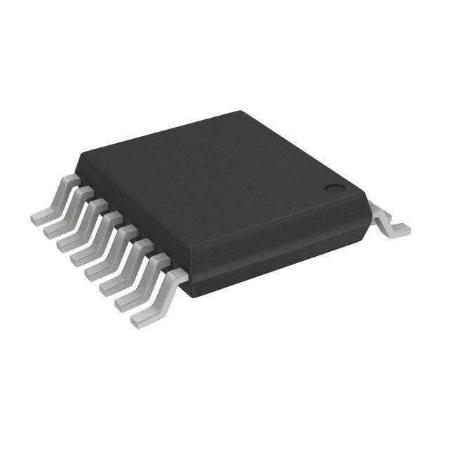
| 供应商器件封装 | 16-SSOP |
| 其它名称 | 296-26145-5 |
| 功能 | Transceiver |
| 包装 | 管件 |
| 协议 | RS232 |
| 单位重量 | 128.600 mg |
| 双工 | 全 |
| 商标 | Texas Instruments |
| 安装类型 | 表面贴装 |
| 安装风格 | SMD/SMT |
| 封装 | Tube |
| 封装/外壳 | 16-SSOP(0.209",5.30mm 宽) |
| 封装/箱体 | SSOP-16 |
| 工作温度 | -40°C ~ 85°C |
| 工作温度范围 | - 40 C to + 85 C |
| 工作电源电压 | 3.3 V, 5 V |
| 工厂包装数量 | 80 |
| 接收器滞后 | 500mV |
| 接收机数量 | 1 Receiver |
| 数据速率 | 250kbps |
| 最大工作温度 | + 85 C |
| 最小工作温度 | - 40 C |
| 标准包装 | 80 |
| 激励器数量 | 1 Driver |
| 电压-电源 | 3 V ~ 5.5 V |
| 电源电流 | 1 mA |
| 类型 | 收发器 |
| 系列 | MAX3221E |
| 驱动器/接收器数 | 1/1 |


- 商务部:美国ITC正式对集成电路等产品启动337调查
- 曝三星4nm工艺存在良率问题 高通将骁龙8 Gen1或转产台积电
- 太阳诱电将投资9.5亿元在常州建新厂生产MLCC 预计2023年完工
- 英特尔发布欧洲新工厂建设计划 深化IDM 2.0 战略
- 台积电先进制程称霸业界 有大客户加持明年业绩稳了
- 达到5530亿美元!SIA预计今年全球半导体销售额将创下新高
- 英特尔拟将自动驾驶子公司Mobileye上市 估值或超500亿美元
- 三星加码芯片和SET,合并消费电子和移动部门,撤换高东真等 CEO
- 三星电子宣布重大人事变动 还合并消费电子和移动部门
- 海关总署:前11个月进口集成电路产品价值2.52万亿元 增长14.8%


PDF Datasheet 数据手册内容提取
Product Sample & Technical Tools & Support & Reference Folder Buy Documents Software Community Design MAX3221E SLLS686B–OCTOBER2005–REVISEDSEPTEMBER2016 MAX3221E 3-V to 5.5-V Single-Channel RS-232 Line Driver/Receiver With ±15-kV IEC ESD Protection 1 Features 3 Description • ESDProtectionforRS-232Pins The MAX3221E is a single driver, single receiver RS- 1 232 solution operating from a single V supply. The – ±15-kVHuman-BodyModel(HBM) CC RS-232 pins provide IEC 61000-4-2 ESD protection. – ±8kV(IEC61000-4-2,ContactDischarge) The device meets the requirements of TIA/EIA-232-F – ±15kV(IEC61000-4-2,Air-GapDischarge) and provides the electrical interface between an asynchronous communication controller and the • MeetsorExceedstheRequirementsofTIA/EIA- serial-port connector. The charge pump and four 232-FandITUv.28Standards small external capacitors allow operation from a • OperatesWith3-Vto5.5-VVCCSupply single 3-V to 5.5-V supply. These devices operate at • Operatesupto250kbit/s data signaling rates up to 250 kbit/s and a maximum of30-V/µsdriveroutputslewrate. • OneDriverandOneReceiver • LowStandbyCurrent:1 µATypical Flexible control options for power management are available. Auto-power down disables driver and • Accepts5-VLogicInputWith3.3-VSupply charge pump when the receiver is disconnected or • Auto-Power-DownFeatureAutomaticallyDisables the remote driver is power down. The drivers can be DriversforPowerSavings manually enabled or disabled. INVALID output goes • AlternativeHigh-SpeedDevice(1Mbit/s) lowwhenreceiverinputisunconnectedorpoweroff. – SN75C3221EandSN65C3221E DeviceInformation(1) 2 Applications PARTNUMBER PACKAGE BODYSIZE(NOM) MAX3221ECDB, • Battery-Powered,Hand-Held,andPortable MAX3221EIDB SSOP(16) 6.20mm×5.30mm Equipment MAX3221ECPW, TSSOP(16) 5.00mm×4.40mm • NotebooksandLaptops MAX3221EIPW • MobilePhonesandWirelessDevices (1) For all available packages, see the orderable addendum at theendofthedatasheet. BlockDiagram 3.3V, 5V POWER FORCEON AUTO- POWERDOWN FORCEOFF EN RX Enable DIN 1 TX 1 DOUT RS-232 250 kb/s IEC 61000-4-2 1 1 ROUT RX RIN RS-232 INVALID STATUS Copyright © 2016,Texas Instruments Incorporated 1 An IMPORTANT NOTICE at the end of this data sheet addresses availability, warranty, changes, use in safety-critical applications, intellectualpropertymattersandotherimportantdisclaimers.PRODUCTIONDATA.
MAX3221E SLLS686B–OCTOBER2005–REVISEDSEPTEMBER2016 www.ti.com Table of Contents 1 Features.................................................................. 1 8 DetailedDescription............................................ 11 2 Applications........................................................... 1 8.1 Overview.................................................................11 3 Description............................................................. 1 8.2 FunctionalBlockDiagram.......................................11 4 RevisionHistory..................................................... 2 8.3 FeatureDescription.................................................11 8.4 DeviceFunctionalModes........................................12 5 PinConfigurationandFunctions......................... 3 9 ApplicationandImplementation........................ 13 6 Specifications......................................................... 4 9.1 ApplicationInformation............................................13 6.1 AbsoluteMaximumRatings......................................4 9.2 TypicalApplication..................................................13 6.2 ESDRatings..............................................................4 10 PowerSupplyRecommendations..................... 16 6.3 RecommendedOperatingConditions.......................4 6.4 ThermalInformation..................................................5 11 Layout................................................................... 16 6.5 ElectricalCharacteristics...........................................5 11.1 LayoutGuidelines.................................................16 6.6 ElectricalCharacteristics:Driver...............................5 11.2 LayoutExample....................................................16 6.7 ElectricalCharacteristics:Receiver..........................6 12 DeviceandDocumentationSupport................. 17 6.8 ElectricalCharacteristics:Auto-PowerDown............6 12.1 ReceivingNotificationofDocumentationUpdates17 6.9 SwitchingCharacteristics:Driver..............................6 12.2 CommunityResource............................................17 6.10 SwitchingCharacteristics:Receiver........................6 12.3 Trademarks...........................................................17 6.11 SwitchingCharacteristics:Auto-PowerDown.........7 12.4 ElectrostaticDischargeCaution............................17 6.12 TypicalCharacteristics............................................7 12.5 Glossary................................................................17 7 ParameterMeasurementInformation..................8 13 Mechanical,Packaging,andOrderable Information........................................................... 17 4 Revision History NOTE:Pagenumbersforpreviousrevisionsmaydifferfrompagenumbersinthecurrentversion. ChangesfromRevisionA(May2006)toRevisionB Page • AddedESDRatingstable,FeatureDescriptionsection,DeviceFunctionalModes,ApplicationandImplementation section,PowerSupplyRecommendationssection,Layoutsection,DeviceandDocumentationSupportsection,and Mechanical,Packaging,andOrderableInformationsection ................................................................................................. 1 • DeletedOrderingInformationtable;seethePOAattheendofthedatasheet ................................................................... 1 • ChangedR thermalvalues:82to92forDBpackageand108to100.3forPWPackage................................................ 5 θJA 2 SubmitDocumentationFeedback Copyright©2005–2016,TexasInstrumentsIncorporated ProductFolderLinks:MAX3221E
MAX3221E www.ti.com SLLS686B–OCTOBER2005–REVISEDSEPTEMBER2016 5 Pin Configuration and Functions DBorPWPackage 16-PinSSOPorTSSOP TopView EN 1 16 FORCEOFF C1+ 2 15 V CC V+ 3 14 GND C1– 4 13 DOUT C2+ 5 12 FORCEON C2– 6 11 DIN V– 7 10 INVALID RIN 8 9 ROUT Not to scale PinFunctions PIN I/O DESCRIPTION NAME NO. C1+ 2 — Positiveterminalsofthevoltage-doublerchargepumpcapacitors C2+ 5 C1– 4 — Negativeterminalsofthevoltage-doublerchargepumpcapacitors C2– 6 DIN 11 I Driverinput DOUT 13 O RS-232driveroutput EN 1 I LowinputenablesreceiverROUToutput.HighinputsetsROUTtohighimpedance. FORCEOFF 16 I Automaticpower-downcontrolinput FORCEON 12 I Automaticpower-downcontrolinput GND 14 — Ground INVALID 10 O Invalidoutputpin.OutputlowwhenRINinputisunpowered. RIN 8 I RS-232receiverinput ROUT 9 O Receiveroutput V 15 — 3-Vto5.5-Vsupplyvoltage CC V+ 3 O 5.5-Vsupplygeneratedbythechargepump V– 7 O –5.5-Vsupplygeneratedbythechargepump Copyright©2005–2016,TexasInstrumentsIncorporated SubmitDocumentationFeedback 3 ProductFolderLinks:MAX3221E
MAX3221E SLLS686B–OCTOBER2005–REVISEDSEPTEMBER2016 www.ti.com 6 Specifications 6.1 Absolute Maximum Ratings overoperatingfree-airtemperaturerange(unlessotherwisenoted)(1) MIN MAX UNIT V Supplyvoltage(2) –0.3 6 V CC V+ Positiveoutputsupplyvoltage(2) –0.3 7 V V– Negativeoutputsupplyvoltage(2) 0.3 –7 V V+–V– Supplyvoltagedifference(2) 13 V DIN,FORCEOFF,FORCEON,EN –0.3 6 V Inputvoltage V I RIN –25 25 DOUT –13.2 13.2 V Outputvoltage V O ROUT,INVALID –0.3 V +0.3 CC T Operatingvirtualjunctiontemperature 150 °C J T Storagetemperature –65 150 °C stg (1) StressesbeyondthoselistedunderAbsoluteMaximumRatingsmaycausepermanentdamagetothedevice.Thesearestressratings only,whichdonotimplyfunctionaloperationofthedeviceattheseoranyotherconditionsbeyondthoseindicatedunderRecommended OperatingConditions.Exposuretoabsolute-maximum-ratedconditionsforextendedperiodsmayaffectdevicereliability. (2) AllvoltagesarewithrespecttonetworkGND. 6.2 ESD Ratings VALUE UNIT Pins8and11 ±15000 Human-bodymodel(HBM),perANSI/ESDA/JEDECJS-001(1) Allotherpins ±2000 V Electrostatic Charged-devicemodel(CDM),perJEDECspecificationJESD22-C101(2) Allpins ±1500 V (ESD) discharge IEC61000-4-2ContactDischarge,DOUTandRIN ±8000 Pins8and11 IEC61000-4-2Air-GapDischarge,DOUTandRIN ±15000 (1) JEDECdocumentJEP155statesthat500-VHBMallowssafemanufacturingwithastandardESDcontrolprocess. (2) JEDECdocumentJEP157statesthat250-VCDMallowssafemanufacturingwithastandardESDcontrolprocess. 6.3 Recommended Operating Conditions SeeFigure11 (1) MIN NOM MAX UNIT V =3.3V 3 3.3 3.6 CC Supplyvoltage V V =5V 4.5 5 5.5 CC V =3.3V 2 CC V Driverandcontrolhigh-levelinputvoltage DIN,FORCEOFF,FORCEON,EN V IH V =5V 2.4 CC V Driverandcontrollow-levelinputvoltage DIN,FORCEOFF,FORCEON,EN 0.8 V IL V Driverandcontrolinputvoltage DIN,FORCEOFF,FORCEON 0 5.5 V I V Receiverinputvoltage –25 25 V I MAX3221EC 0 70 T Operatingfree-airtemperature °C A MAX3221EI –40 85 (1) TestconditionsareC1–C4=0.1µFatV =3.3V±0.3V;C1=0.047µF,C2–C4=0.33µFatV =5V±0.5V. CC CC 4 SubmitDocumentationFeedback Copyright©2005–2016,TexasInstrumentsIncorporated ProductFolderLinks:MAX3221E
MAX3221E www.ti.com SLLS686B–OCTOBER2005–REVISEDSEPTEMBER2016 6.4 Thermal Information MAX3221E THERMALMETRIC(1) DB(SSOP) PW(TSSOP) UNIT 16PINS 16PINS R Junction-to-ambientthermalresistance 92 100.3 °C/W θJA R Junction-to-case(top)thermalresistance 42.8 35.6 °C/W θJC(top) R Junction-to-boardthermalresistance 42.4 45.1 °C/W θJB ψ Junction-to-topcharacterizationparameter 9.1 2.5 °C/W JT ψ Junction-to-boardcharacterizationparameter 41.9 44.6 °C/W JB (1) Formoreinformationabouttraditionalandnewthermalmetrics,seetheSemiconductorandICPackageThermalMetricsapplication report. 6.5 Electrical Characteristics overrecommendedrangesofsupplyvoltageandoperatingfree-airtemperature(unlessotherwisenoted)(1) PARAMETER TESTCONDITIONS MIN TYP(2) MAX UNIT FORCEOFF, I Inputleakagecurrent ±0.01 ±1 µA I FORCEON,EN Noload, Auto-powerdown FORCEOFFand 0.3 1 mA disabled FORCEONatV CC V =3.3Vor5V, Noload, I Supplycurrent Poweredoff CC 1 10 CC T =25°C FORCEOFFatGND A Noload,FORCEOFFatV , µA Auto-powerdown CC FORCEONatGND, 1 10 enabled AllRINareopenorgrounded (1) TestconditionsareC1–C4=0.1µFatV =3.3V±0.3V;C1=0.047µF,C2–C4=0.33µFatV =5V±0.5V. CC CC (2) AlltypicalvaluesareatV =3.3VorV =5V,andT =25°C. CC CC A 6.6 Electrical Characteristics: Driver overrecommendedrangesofsupplyvoltageandoperatingfree-airtemperature(unlessotherwisenoted)(1) PARAMETER TESTCONDITIONS MIN TYP(2) MAX UNIT V High-leveloutputvoltage DOUTatR =3kΩtoGND, DIN=GND 5 5.4 V OH L V Low-leveloutputvoltage DOUTatR =3kΩtoGND, DIN=V –5 –5.4 V OL L CC I High-levelinputcurrent V =V ±0.01 ±1 µA IH I CC I Low-levelinputcurrent V =GND ±0.01 ±1 µA IL I Short-circuit VCC=3.6V, VO=0V ±35 ±60 IOS outputcurrent(3) V =5.5V, V =0V ±35 ±60 mA CC O r Outputresistance V ,V+,andV–=0V, V =±2V 300 10M Ω o CC O V =±12V, V =3Vto3.6V ±25 O CC I Outputleakagecurrent FORCEOFF=GND µA off V =±10V, V =4.5Vto5.5V ±25 O CC (1) TestconditionsareC1–C4=0.1µFatV =3.3V±0.3V;C1=0.047µF,C2–C4=0.33µFatV =5V±0.5V. CC CC (2) AlltypicalvaluesareatV =3.3VorV =5V,andT =25°C. CC CC A (3) Short-circuitdurationsshouldbecontrolledtopreventexceedingthedeviceabsolutepower-dissipationratings,andnotmorethanone outputshouldbeshortedatatime. Copyright©2005–2016,TexasInstrumentsIncorporated SubmitDocumentationFeedback 5 ProductFolderLinks:MAX3221E
MAX3221E SLLS686B–OCTOBER2005–REVISEDSEPTEMBER2016 www.ti.com 6.7 Electrical Characteristics: Receiver overrecommendedrangesofsupplyvoltageandoperatingfree-airtemperature(unlessotherwisenoted)(1) PARAMETER TESTCONDITIONS MIN TYP(2) MAX UNIT V High-leveloutputvoltage I =–1mA V –0.6 V –0.1 V OH OH CC CC V Low-leveloutputvoltage I =1.6mA 0.4 V OL OL V =3.3V 1.6 2.4 CC V Positive-goinginputthresholdvoltage V IT+ V =5V 1.9 2.4 CC V =3.3V 0.6 1.1 CC V Negative-goinginputthresholdvoltage V IT– V =5V 0.8 1.4 CC V Inputhysteresis(V –V ) 0.5 V hys IT+ IT– I Outputleakagecurrent EN=V ±0.05 ±10 µA off CC r Inputresistance V =±3Vto±25V 3 5 7 kΩ i I (1) TestconditionsareC1–C4=0.1µFatV =3.3V±0.3V;C1=0.047µF,C2–C4=0.33µFatV =5V±0.5V. CC CC (2) AlltypicalvaluesareatV =3.3VorV =5V,andT =25°C. CC CC A 6.8 Electrical Characteristics: Auto-Power Down overrecommendedrangesofsupplyvoltageandoperatingfree-airtemperature(unlessotherwisenoted) PARAMETER TESTCONDITIONS MIN MAX UNIT Receiverinputthreshold V FORCEON=GND, FORCEOFF=V 2.7 V T+(valid) forINVALIDhigh-leveloutputvoltage CC Receiverinputthreshold V FORCEON=GND, FORCEOFF=V –2.7 V T–(valid) forINVALIDhigh-leveloutputvoltage CC Receiverinputthreshold V FORCEON=GND, FORCEOFF=V –0.3 0.3 V T(invalid) forINVALIDlow-leveloutputvoltage CC I =–1mA,FORCEON=GND, V INVALIDhigh-leveloutputvoltage OH V –0.6 V OH FORCEOFF=V CC CC I =1.6mA,FORCEON=GND, V INVALIDlow-leveloutputvoltage OL 0.4 V OL FORCEOFF=V CC 6.9 Switching Characteristics: Driver overrecommendedrangesofsupplyvoltageandoperatingfree-airtemperature(unlessotherwisenoted)(1) PARAMETER TESTCONDITIONS MIN TYP(2) MAX UNIT Maximumdatarate C =1000pF, R =3kΩ, 150 250 kbit/s L L t Pulseskew(3) C =150pFto2500pF, R =3kΩto7kΩ, SeeFigure6 100 ns sk(p) L L Slewrate, C =150pFto1000pF 6 30 V =3.3V, L SR(tr) transitionregion CC V/µs (seeFigure5) RL=3kΩto7kΩ CL=150pFto2500pF 4 30 (1) TestconditionsareC1–C4=0.1µFatV =3.3V±0.3V;C1=0.047µF,C2–C4=0.33µFatV =5V±0.5V. CC CC (2) AlltypicalvaluesareatV =3.3VorV =5V,andT =25°C. CC CC A (3) Pulseskewisdefinedas|t –t |ofeachchannelofthesamedevice. PLH PHL 6.10 Switching Characteristics: Receiver overrecommendedrangesofsupplyvoltageandoperatingfree-airtemperature(unlessotherwisenoted)(1) PARAMETER TESTCONDITIONS TYP(2) UNIT t Propagationdelaytime,low-tohigh-leveloutput C =150pF,SeeFigure7 150 ns PLH L t Propagationdelaytime,high-tolow-leveloutput C =150pF,SeeFigure7 150 ns PHL L t Outputenabletime C =150pF,R =3kΩ,SeeFigure8 200 ns en L L t Outputdisabletime C =150pF,R =3kΩ,SeeFigure8 200 ns dis L L t Pulseskew(3) SeeFigure7 50 ns sk(p) (1) TestconditionsareC1–C4=0.1µFatV =3.3V±0.3V;C1=0.047µF,C2–C4=0.33µFatV =5V±0.5V. CC CC (2) AlltypicalvaluesareatV =3.3VorV =5V,andT =25°C. CC CC A (3) Pulseskewisdefinedas|t –t |ofeachchannelofthesamedevice. PLH PHL 6 SubmitDocumentationFeedback Copyright©2005–2016,TexasInstrumentsIncorporated ProductFolderLinks:MAX3221E
MAX3221E www.ti.com SLLS686B–OCTOBER2005–REVISEDSEPTEMBER2016 6.11 Switching Characteristics: Auto-Power Down overrecommendedrangesofsupplyvoltageandoperatingfree-airtemperature(unlessotherwisenoted) PARAMETER TYP(1) UNIT t Propagationdelaytime,low-tohigh-leveloutput 1 µs valid t Propagationdelaytime,high-tolow-leveloutput 30 µs invalid t Supplyenabletime 100 µs en (1) AlltypicalvaluesareatV =3.3VorV =5V,andT =25°C. CC CC A 6.12 Typical Characteristics T =25°C;V =3.3V A CC 1.2 3.5 1 3 2.5 V) 0.8 V) e ( e ( g g 2 a a olt 0.6 olt V V T T 1.5 U U O 0.4 O R R 1 0.2 0.5 0 0 0 1 2 3 4 5 6 7 8 9 10 0 1 2 3 4 5 6 7 8 9 10 ROUT Current (mA) ROUT Current (mA) D001 D002 Figure1.ReceiverVOLvsLoadCurrent Figure2.ReceiverVOHvsLoadCurrent 6 0 5 -1 V) 4 V) -2 e ( e ( g g a a olt 3 olt -3 V V T T U U O 2 O -4 D D 1 -5 0 -6 0 3 6 9 12 15 18 21 24 27 30 0 3 6 9 12 15 18 21 24 27 30 DOUT Current (mA) DOUT Current (mA) D003 D004 Figure3.DriverVOHvsLoadCurrent Figure4.DriverVOLvsLoadCurrent Copyright©2005–2016,TexasInstrumentsIncorporated SubmitDocumentationFeedback 7 ProductFolderLinks:MAX3221E
MAX3221E SLLS686B–OCTOBER2005–REVISEDSEPTEMBER2016 www.ti.com 7 Parameter Measurement Information 3 V Input RS-232 0 V Output Generator (see Note B) 50Ω CL tTHL tTLH RL (see NoteA) VOH 3 V 3 V 3 V Output FORCEOFF −3 V −3 V VOL 6V SR(tr) = TESTCIRCUIT t ort VOLTAGEWAVEFORMS THL TLH A. C includesprobeandjigcapacitance. L B. The pulse generator has the following characteristics: PRR = 250 kbps, Z = 50 Ω, 50% duty cycle, t ≤ 10 ns, O r t ≤10ns. f Figure5. DriverSlewRate 3 V RS-232 Input 1.5V 1.5 V Output 0 V Generator 50Ω (see Note B) CL tPHL tPLH RL (see NoteA) VOH 3 V Output 50% 50% FORCEOFF VOL TESTCIRCUIT VOLTAGEWAVEFORMS A. C includesprobeandjigcapacitance. L B. The pulse generator has the following characteristics: PRR = 250 kbps, Z = 50 Ω, 50% duty cycle, t ≤ 10 ns, O r t ≤10ns. f Figure6. DriverPulseSkew 3 V or 0 V 3 V FORCEON Input 1.5 V 1.5 V −3 V Output Generator 50Ω tPHL tPLH (see Note B) CL (see NoteA) 3 V VOH FORCEOFF Output 50% 50% VOL TESTCIRCUIT VOLTAGEWAVEFORMS A. C includesprobeandjigcapacitance. L B. Thepulsegeneratorhasthefollowingcharacteristics:Z =50Ω,50%dutycycle,t ≤10ns,t ≤10ns. O r f Figure7. ReceiverPropagationDelayTimes 8 SubmitDocumentationFeedback Copyright©2005–2016,TexasInstrumentsIncorporated ProductFolderLinks:MAX3221E
MAX3221E www.ti.com SLLS686B–OCTOBER2005–REVISEDSEPTEMBER2016 Parameter Measurement Information (continued) 3 V Input 1.5 V 1.5 V VCC GND 3 V or 0 V 0 V S1 FORCEON tPHZ tPZH RL (S1 at GND) (S1atGND) 3 V or 0 V Output VOH Output 50% CL 0.3 V (see NoteA) EN tPLZ tPZL Generator (S1 at VCC) (S1 at VCC) 50Ω (see Note B) 0.3 V Output 50% VOL TEST CIRCUIT VOLTAGE WAVEFORMS A. C includesprobeandjigcapacitance. L B. Thepulsegeneratorhasthefollowingcharacteristics:Z =50Ω,50%dutycycle,t ≤10ns,t ≤10ns. O r f C. t andt arethesameast . PLZ PHZ dis D. t andt arethesameast . PZL PZH en Figure8. ReceiverEnableandDisableTimes Copyright©2005–2016,TexasInstrumentsIncorporated SubmitDocumentationFeedback 9 ProductFolderLinks:MAX3221E
MAX3221E SLLS686B–OCTOBER2005–REVISEDSEPTEMBER2016 www.ti.com Parameter Measurement Information (continued) 3 V 2.7 V 2.7 V Receiver 0 V Input 0 V ROUT −2.7 V −2.7 V Generator −3 V 50Ω (see Note B) tinvalid tvalid VCC 50% VCC 50% VCC INVALID 0 V Output Auto- INVALID ten powerdown CL= 30 pF V+ ≈V+ (see NoteA) 0.3 V FORCEOFF Supply VCC Voltages 0 V DIN DOUT 0.3 V FORCEON V− ≈V− TESTCIRCUIT VOLTAGEWAVEFORMS ValidRS-232Level,INVALIDHigh 2.7 V Indeterminate 0.3 V IfSignalRemainsWithinThisRegion 0 V For More Than 30µs,INVALIDIs Low† −0.3 V Indeterminate −2.7 V ValidRS-232Level,INVALIDHigh †Auto-powerdowndisables drivers and reduces supply currentto1µA. Figure9. INVALID PropagationDelayTimesandDriverEnablingTime 10 SubmitDocumentationFeedback Copyright©2005–2016,TexasInstrumentsIncorporated ProductFolderLinks:MAX3221E
MAX3221E www.ti.com SLLS686B–OCTOBER2005–REVISEDSEPTEMBER2016 8 Detailed Description 8.1 Overview The MAX3221E is a single driver, single receiver RS-232 solution operating from a single V supply. The RS- CC 232 pins provide IEC 61000-4-2 ESD protection. The device meets the requirements of TIA/EIA-232-F and provides the electrical interface between an asynchronous communication controller and the serial-port connector. The charge pump and four small external capacitors allow operation from a single 3-V to 5.5-V supply. These devices operate at data signaling rates up to 250 kbit/s and a maximum of 30-V/µs driver output slewrate. Flexible control options for power management are available when the serial port is inactive. The auto-power- down feature functions when FORCEON is low and FORCEOFF is high. During this mode of operation, if the device does not sense a valid RS-232 signal on the receiver input, the driver output is disabled. If FORCEOFF is set low and EN is high, both the driver and receiver are shut off, and the supply current is reduced to 1 µA. Disconnecting the serial port or turning off the peripheral drivers causes the auto-power-down condition to occur. Auto-power down can be disabled when FORCEON and FORCEOFF are high. With auto-power down enabled, the device is activated automatically when a valid signal is applied to the receiver input. The INVALID output notifies the user if an RS-232 signal is present at the receiver input. INVALID is high (valid data) if the receiver input voltage is greater than 2.7 V or less than –2.7 V, or has been between –0.3 V and 0.3 V for less than 30 µs. INVALID is low (invalid data) if the receiver input voltage is between –0.3 V and 0.3 V for more than 30 µs. SeeFigure5forreceiverinputlevels. 8.2 Functional Block Diagram 3.3V, 5V POWER FORCEON AUTO- POWERDOWN FORCEOFF EN RX Enable DIN 1 TX 1 DOUT RS-232 250 kb/s IEC 61000-4-2 1 1 ROUT RX RIN RS-232 INVALID STATUS Copyright © 2016,Texas Instruments Incorporated Figure10. LogicDiagram(PositiveLogic) 8.3 Feature Description 8.3.1 Power The power block increases, inverts, and regulates voltage at V+ and V- pins using a charge pump that requires four external capacitors. Auto-power-down feature for driver is controlled by FORCEON and FORCEOFF inputs. Receiver is controlled by EN input. When MAX3221E is unpowered, it can be safely connected to an active remoteRS-232device. 8.3.2 RS-232Driver OnedriverinterfacesstandardlogiclevelstoRS-232levels.DINinputmustbevalidhighorlow. Copyright©2005–2016,TexasInstrumentsIncorporated SubmitDocumentationFeedback 11 ProductFolderLinks:MAX3221E
MAX3221E SLLS686B–OCTOBER2005–REVISEDSEPTEMBER2016 www.ti.com Feature Description (continued) 8.3.3 RS-232Receiver One receiver interfaces RS-232 levels to standard logic levels. An open input results in a high output on ROUT. RIN input includes an internal standard RS-232 load. A logic high input on the EN pin shuts down the receiver output. 8.3.4 RS-232Status The INVALID output goes low when RIN input is unpowered for more than 30 µs. The INVALID output goes high when receiver has a valid input. The INVALID output is active when V is powered irregardless of FORCEON cc andFORCEOFF inputs(seeTable3). 8.4 Device Functional Modes Table 1, Table 2, and Table 3 show the behavior of the driver, receiver, and INVALID features under all possible relevantcombinationsofinputs. Table1.FunctionTablesEachDriver(1) INPUTS OUTPUT DIN FORCEON FORCEOFF VALIDRIN DOUT DRIVERSTATUS RS-232LEVEL X X L X Z Poweredoff L H H X H Normaloperationwith H H H X L auto-powerdowndisabled L L H Yes H Normaloperationwith H L H Yes L auto-powerdownenabled L L H No Z Poweredoffby H L H No Z auto-powerdownfeature (1) H=highlevel,L=lowlevel,X=irrelevant,Z=highimpedance Table2.EachReceiver(1) INPUTS OUTPUT RIN EN VALIDRIN ROUT RS-232LEVEL L L X H H L X L X H X Z Open L No H (1) H=highlevel,L=lowlevel,X=irrelevant,Z=highimpedance(off), Open=disconnectedinputorconnecteddriveroff Table3.INVALID(1) INPUTS OUTPUT RIN FORCEON FORCEOFF EN INVALID L X X X H H X X X H Open X X X L (1) H=highlevel,L=lowlevel,X=irrelevant,Z=highimpedance(off),Open=inputdisconnectedorconnecteddriveroff 12 SubmitDocumentationFeedback Copyright©2005–2016,TexasInstrumentsIncorporated ProductFolderLinks:MAX3221E
MAX3221E www.ti.com SLLS686B–OCTOBER2005–REVISEDSEPTEMBER2016 9 Application and Implementation NOTE Information in the following applications sections is not part of the TI component specification, and TI does not warrant its accuracy or completeness. TI’s customers are responsible for determining suitability of components for their purposes. Customers should validateandtesttheirdesignimplementationtoconfirmsystemfunctionality. 9.1 Application Information The MAX3221E line driver and receiver is a specialized device for 3-V to 5.5-V RS-232 communication applications. This application is a generic implementation of this device with all required external components. Forproperoperation,addcapacitorsasshowninFigure11. 9.2 Typical Application ROUT and DIN connect to UART or general purpose logic lines. FORCEON and FORCEOFF may be connected general purpose logic lines or tied to ground or V . INVALID may be connected to a general purpose logic line CC or left unconnected. RIN and DOUT lines connect to a RS-232 connector or cable. DIN, FORCEON, and FORCEOFF inputsmustnotbeleftunconnected. Copyright©2005–2016,TexasInstrumentsIncorporated SubmitDocumentationFeedback 13 ProductFolderLinks:MAX3221E
MAX3221E SLLS686B–OCTOBER2005–REVISEDSEPTEMBER2016 www.ti.com Typical Application (continued) 1 16 EN FORCEOFF 2 C1+ VCC 15 + CBYPASS= 0.1mF 3 − + + V+ Auto- 14 C1 C3(1) Powerdown GND − − 4 C1− 13 5 DOUT C2+ + 12 C2 FORCEON − 6 C2− 11 DIN 7 V− − 10 C4 INVALID + 8 9 RIN ROUT 5 kW (1) C3 can be connected to VCCor GND. NOTES: A. Resistor values shown are nominal. B. Nonpolarized ceramic capacitors are acceptable. If polarized tantalum or electrolytic capacitors are used, they should be connected as shown. VCCvs CAPACITOR VALUES VCC C1 C2, C3, and C4 3.3 V± 0.3 V 0.1mF 0.1mF 5 V± 0.5 V 0.047mF 0.33mF 3 V to 5.5 V 0.1mF 0.47mF Copyright © 2016,Texas Instruments Incorporated Figure11. TypicalOperatingCircuitandCapacitorValues 9.2.1 DesignRequirements • RecommendedV is3.3Vor5V. CC – 3Vto5.5Visalsopossible • Maximumrecommendedbitrateis250kbps. • UsecapacitorsasshowninFigure11. 9.2.2 DetailedDesignProcedure • DIN, FORCEOFF andFORCEONinputsmustbeconnectedtovalidloworhighlogiclevels. • SelectcapacitorvaluesbasedonVCClevelforbestperformance. 14 SubmitDocumentationFeedback Copyright©2005–2016,TexasInstrumentsIncorporated ProductFolderLinks:MAX3221E
MAX3221E www.ti.com SLLS686B–OCTOBER2005–REVISEDSEPTEMBER2016 Typical Application (continued) 9.2.3 ApplicationCurves 8 8 DIN DIN DOUT DOUT 6 6 ROUT ROUT V) 4 V) 4 e ( e ( g g olta 2 olta 2 V V m m or 0 or 0 ef ef v v Wa -2 Wa -2 -4 -4 -6 -6 0 1 2 3 4 5 6 7 8 9 10 0 1 2 3 4 5 6 7 8 9 10 Time (us) Time (us) D005 D006 Figure12.LoopbackWaveforms Figure13.LoopbackWaveformswith1-nFload V =3.3V,DataRate250kbit/s V =3.3V,DataRate250kbit/s CC CC Copyright©2005–2016,TexasInstrumentsIncorporated SubmitDocumentationFeedback 15 ProductFolderLinks:MAX3221E
MAX3221E SLLS686B–OCTOBER2005–REVISEDSEPTEMBER2016 www.ti.com 10 Power Supply Recommendations TIrecommendsa0.1-µFcapacitortofilternoiseonthepowersupplypin.Foradditionalfiltercapability,a 0.01-μF capacitor may be added in parallel as well. Power supply input voltage is recommended to be any valid levelinRecommendedOperatingConditions. 11 Layout 11.1 Layout Guidelines Keep the external capacitor traces short. This is more important on C1 and C2 nodes that have the fastest rise and fall times. Make the impedance from MAX3221E ground pin and circuit board's ground plane as low as possibleforbestESDperformance.Usewidemetalandmultipleviasonbothsidesofgroundpin. 11.2 Layout Example 1 EN FORCEOFF 16 Ground C3 2 C1+ VCC 15 VCC (cid:19)(cid:17)(cid:20)PF C1 3 V+ GND 14 Ground 4 C1- DOUT 13 5 C2+ FORCEON 12 C2 6 C2- DIN 11 Ground 7 V- INVALID 10 C4 8 RIN ROUT 9 Figure14. MAX3221ELayoutExample 16 SubmitDocumentationFeedback Copyright©2005–2016,TexasInstrumentsIncorporated ProductFolderLinks:MAX3221E
MAX3221E www.ti.com SLLS686B–OCTOBER2005–REVISEDSEPTEMBER2016 12 Device and Documentation Support 12.1 Receiving Notification of Documentation Updates To receive notification of documentation updates, navigate to the device product folder on ti.com. In the upper right corner, click on Alert me to register and receive a weekly digest of any product information that has changed.Forchangedetails,reviewtherevisionhistoryincludedinanyreviseddocument. 12.2 Community Resource The following links connect to TI community resources. Linked contents are provided "AS IS" by the respective contributors. They do not constitute TI specifications and do not necessarily reflect TI's views; see TI's Terms of Use. TIE2E™OnlineCommunity TI'sEngineer-to-Engineer(E2E)Community.Createdtofostercollaboration amongengineers.Ate2e.ti.com,youcanaskquestions,shareknowledge,exploreideasandhelp solveproblemswithfellowengineers. DesignSupport TI'sDesignSupport QuicklyfindhelpfulE2Eforumsalongwithdesignsupporttoolsand contactinformationfortechnicalsupport. 12.3 Trademarks E2EisatrademarkofTexasInstruments. Allothertrademarksarethepropertyoftheirrespectiveowners. 12.4 Electrostatic Discharge Caution Thesedeviceshavelimitedbuilt-inESDprotection.Theleadsshouldbeshortedtogetherorthedeviceplacedinconductivefoam duringstorageorhandlingtopreventelectrostaticdamagetotheMOSgates. 12.5 Glossary SLYZ022—TIGlossary. Thisglossarylistsandexplainsterms,acronyms,anddefinitions. 13 Mechanical, Packaging, and Orderable Information The following pages include mechanical, packaging, and orderable information. This information is the most current data available for the designated devices. This data is subject to change without notice and revision of thisdocument.Forbrowser-basedversionsofthisdatasheet,refertotheleft-handnavigation. Copyright©2005–2016,TexasInstrumentsIncorporated SubmitDocumentationFeedback 17 ProductFolderLinks:MAX3221E
PACKAGE OPTION ADDENDUM www.ti.com 24-Aug-2018 PACKAGING INFORMATION Orderable Device Status Package Type Package Pins Package Eco Plan Lead/Ball Finish MSL Peak Temp Op Temp (°C) Device Marking Samples (1) Drawing Qty (2) (6) (3) (4/5) MAX3221ECDB ACTIVE SSOP DB 16 80 Green (RoHS CU NIPDAU Level-1-260C-UNLIM 0 to 70 MP221EC & no Sb/Br) MAX3221ECDBR ACTIVE SSOP DB 16 2000 Green (RoHS CU NIPDAU Level-1-260C-UNLIM 0 to 70 MP221EC & no Sb/Br) MAX3221ECDBRG4 ACTIVE SSOP DB 16 2000 Green (RoHS CU NIPDAU Level-1-260C-UNLIM 0 to 70 MP221EC & no Sb/Br) MAX3221ECPW ACTIVE TSSOP PW 16 90 Green (RoHS CU NIPDAU Level-1-260C-UNLIM 0 to 70 MP221EC & no Sb/Br) MAX3221ECPWE4 ACTIVE TSSOP PW 16 90 Green (RoHS CU NIPDAU Level-1-260C-UNLIM 0 to 70 MP221EC & no Sb/Br) MAX3221ECPWG4 ACTIVE TSSOP PW 16 90 Green (RoHS CU NIPDAU Level-1-260C-UNLIM 0 to 70 MP221EC & no Sb/Br) MAX3221ECPWR ACTIVE TSSOP PW 16 2000 Green (RoHS CU NIPDAU Level-1-260C-UNLIM 0 to 70 MP221EC & no Sb/Br) MAX3221EIDB ACTIVE SSOP DB 16 80 Green (RoHS CU NIPDAU Level-1-260C-UNLIM -40 to 85 MP221EI & no Sb/Br) MAX3221EIDBG4 ACTIVE SSOP DB 16 80 Green (RoHS CU NIPDAU Level-1-260C-UNLIM -40 to 85 MP221EI & no Sb/Br) MAX3221EIDBR ACTIVE SSOP DB 16 2000 Green (RoHS CU NIPDAU Level-1-260C-UNLIM -40 to 85 MP221EI & no Sb/Br) MAX3221EIDBRG4 ACTIVE SSOP DB 16 2000 Green (RoHS CU NIPDAU Level-1-260C-UNLIM -40 to 85 MP221EI & no Sb/Br) MAX3221EIPW ACTIVE TSSOP PW 16 90 Green (RoHS CU NIPDAU Level-1-260C-UNLIM -40 to 85 MP221EI & no Sb/Br) MAX3221EIPWE4 ACTIVE TSSOP PW 16 90 Green (RoHS CU NIPDAU Level-1-260C-UNLIM -40 to 85 MP221EI & no Sb/Br) MAX3221EIPWG4 ACTIVE TSSOP PW 16 90 Green (RoHS CU NIPDAU Level-1-260C-UNLIM -40 to 85 MP221EI & no Sb/Br) MAX3221EIPWR ACTIVE TSSOP PW 16 2000 Green (RoHS CU NIPDAU | CU SN Level-1-260C-UNLIM -40 to 85 MP221EI & no Sb/Br) MAX3221EIPWRG4 ACTIVE TSSOP PW 16 2000 Green (RoHS CU NIPDAU Level-1-260C-UNLIM -40 to 85 MP221EI & no Sb/Br) (1) The marketing status values are defined as follows: ACTIVE: Product device recommended for new designs. Addendum-Page 1
PACKAGE OPTION ADDENDUM www.ti.com 24-Aug-2018 LIFEBUY: TI has announced that the device will be discontinued, and a lifetime-buy period is in effect. NRND: Not recommended for new designs. Device is in production to support existing customers, but TI does not recommend using this part in a new design. PREVIEW: Device has been announced but is not in production. Samples may or may not be available. OBSOLETE: TI has discontinued the production of the device. (2) RoHS: TI defines "RoHS" to mean semiconductor products that are compliant with the current EU RoHS requirements for all 10 RoHS substances, including the requirement that RoHS substance do not exceed 0.1% by weight in homogeneous materials. Where designed to be soldered at high temperatures, "RoHS" products are suitable for use in specified lead-free processes. TI may reference these types of products as "Pb-Free". RoHS Exempt: TI defines "RoHS Exempt" to mean products that contain lead but are compliant with EU RoHS pursuant to a specific EU RoHS exemption. Green: TI defines "Green" to mean the content of Chlorine (Cl) and Bromine (Br) based flame retardants meet JS709B low halogen requirements of <=1000ppm threshold. Antimony trioxide based flame retardants must also meet the <=1000ppm threshold requirement. (3) MSL, Peak Temp. - The Moisture Sensitivity Level rating according to the JEDEC industry standard classifications, and peak solder temperature. (4) There may be additional marking, which relates to the logo, the lot trace code information, or the environmental category on the device. (5) Multiple Device Markings will be inside parentheses. Only one Device Marking contained in parentheses and separated by a "~" will appear on a device. If a line is indented then it is a continuation of the previous line and the two combined represent the entire Device Marking for that device. (6) Lead/Ball Finish - Orderable Devices may have multiple material finish options. Finish options are separated by a vertical ruled line. Lead/Ball Finish values may wrap to two lines if the finish value exceeds the maximum column width. Important Information and Disclaimer:The information provided on this page represents TI's knowledge and belief as of the date that it is provided. TI bases its knowledge and belief on information provided by third parties, and makes no representation or warranty as to the accuracy of such information. Efforts are underway to better integrate information from third parties. TI has taken and continues to take reasonable steps to provide representative and accurate information but may not have conducted destructive testing or chemical analysis on incoming materials and chemicals. TI and TI suppliers consider certain information to be proprietary, and thus CAS numbers and other limited information may not be available for release. In no event shall TI's liability arising out of such information exceed the total purchase price of the TI part(s) at issue in this document sold by TI to Customer on an annual basis. Addendum-Page 2
PACKAGE MATERIALS INFORMATION www.ti.com 20-Dec-2018 TAPE AND REEL INFORMATION *Alldimensionsarenominal Device Package Package Pins SPQ Reel Reel A0 B0 K0 P1 W Pin1 Type Drawing Diameter Width (mm) (mm) (mm) (mm) (mm) Quadrant (mm) W1(mm) MAX3221ECPWR TSSOP PW 16 2000 330.0 12.4 6.9 5.6 1.6 8.0 12.0 Q1 MAX3221EIPWR TSSOP PW 16 2000 330.0 12.4 6.9 5.6 1.6 8.0 12.0 Q1 MAX3221EIPWR TSSOP PW 16 2000 330.0 12.4 6.9 5.6 1.6 8.0 12.0 Q1 MAX3221EIPWRG4 TSSOP PW 16 2000 330.0 12.4 6.9 5.6 1.6 8.0 12.0 Q1 PackMaterials-Page1
PACKAGE MATERIALS INFORMATION www.ti.com 20-Dec-2018 *Alldimensionsarenominal Device PackageType PackageDrawing Pins SPQ Length(mm) Width(mm) Height(mm) MAX3221ECPWR TSSOP PW 16 2000 367.0 367.0 35.0 MAX3221EIPWR TSSOP PW 16 2000 367.0 367.0 35.0 MAX3221EIPWR TSSOP PW 16 2000 364.0 364.0 27.0 MAX3221EIPWRG4 TSSOP PW 16 2000 367.0 367.0 35.0 PackMaterials-Page2
MECHANICAL DATA MSSO002E – JANUARY 1995 – REVISED DECEMBER 2001 DB (R-PDSO-G**) PLASTIC SMALL-OUTLINE 28 PINS SHOWN 0,38 0,65 0,15 M 0,22 28 15 0,25 0,09 5,60 8,20 5,00 7,40 Gage Plane 1 14 0,25 A 0°–(cid:1)8° 0,95 0,55 Seating Plane 2,00 MAX 0,05 MIN 0,10 PINS ** 14 16 20 24 28 30 38 DIM A MAX 6,50 6,50 7,50 8,50 10,50 10,50 12,90 A MIN 5,90 5,90 6,90 7,90 9,90 9,90 12,30 4040065/E 12/01 NOTES: A. All linear dimensions are in millimeters. B. This drawing is subject to change without notice. C. Body dimensions do not include mold flash or protrusion not to exceed 0,15. D. Falls within JEDEC MO-150 • POST OFFICE BOX 655303 DALLAS, TEXAS 75265
PACKAGE OUTLINE PW0016A TSSOP - 1.2 mm max height SCALE 2.500 SMALL OUTLINE PACKAGE SEATING PLANE C 6.6 TYP 6.2 A 0.1 C PIN 1 INDEX AREA 14X 0.65 16 1 2X 5.1 4.55 4.9 NOTE 3 8 9 0.30 B 4.5 16X 0.19 1.2 MAX 4.3 0.1 C A B NOTE 4 (0.15) TYP SEE DETAIL A 0.25 GAGE PLANE 0.15 0.05 0.75 0.50 0 -8 DETA 20AIL A TYPICAL 4220204/A 02/2017 NOTES: 1. All linear dimensions are in millimeters. Any dimensions in parenthesis are for reference only. Dimensioning and tolerancing per ASME Y14.5M. 2. This drawing is subject to change without notice. 3. This dimension does not include mold flash, protrusions, or gate burrs. Mold flash, protrusions, or gate burrs shall not exceed 0.15 mm per side. 4. This dimension does not include interlead flash. Interlead flash shall not exceed 0.25 mm per side. 5. Reference JEDEC registration MO-153. www.ti.com
EXAMPLE BOARD LAYOUT PW0016A TSSOP - 1.2 mm max height SMALL OUTLINE PACKAGE 16X (1.5) SYMM (R0.05) TYP 1 16X (0.45) 16 SYMM 14X (0.65) 8 9 (5.8) LAND PATTERN EXAMPLE EXPOSED METAL SHOWN SCALE: 10X SOLDER MASK METAL UNDER SOLDER MASK OPENING METAL SOLDER MASK OPENING EXPOSED METAL EXPOSED METAL 0.05 MAX 0.05 MIN ALL AROUND ALL AROUND NON-SOLDER MASK SOLDER MASK DEFINED DEFINED (PREFERRED) SOLDE15.000R MASK DETAILS 4220204/A 02/2017 NOTES: (continued) 6. Publication IPC-7351 may have alternate designs. 7. Solder mask tolerances between and around signal pads can vary based on board fabrication site. www.ti.com
EXAMPLE STENCIL DESIGN PW0016A TSSOP - 1.2 mm max height SMALL OUTLINE PACKAGE 16X (1.5) SYMM (R0.05) TYP 1 16X (0.45) 16 SYMM 14X (0.65) 8 9 (5.8) SOLDER PASTE EXAMPLE BASED ON 0.125 mm THICK STENCIL SCALE: 10X 4220204/A 02/2017 NOTES: (continued) 8. Laser cutting apertures with trapezoidal walls and rounded corners may offer better paste release. IPC-7525 may have alternate design recommendations. 9. Board assembly site may have different recommendations for stencil design. www.ti.com
IMPORTANTNOTICEANDDISCLAIMER TIPROVIDESTECHNICALANDRELIABILITYDATA(INCLUDINGDATASHEETS),DESIGNRESOURCES(INCLUDINGREFERENCE DESIGNS),APPLICATIONOROTHERDESIGNADVICE,WEBTOOLS,SAFETYINFORMATION,ANDOTHERRESOURCES“ASIS” ANDWITHALLFAULTS,ANDDISCLAIMSALLWARRANTIES,EXPRESSANDIMPLIED,INCLUDINGWITHOUTLIMITATIONANY IMPLIEDWARRANTIESOFMERCHANTABILITY,FITNESSFORAPARTICULARPURPOSEORNON-INFRINGEMENTOFTHIRD PARTYINTELLECTUALPROPERTYRIGHTS. TheseresourcesareintendedforskilleddevelopersdesigningwithTIproducts.Youaresolelyresponsiblefor(1)selectingtheappropriate TIproductsforyourapplication,(2)designing,validatingandtestingyourapplication,and(3)ensuringyourapplicationmeetsapplicable standards,andanyothersafety,security,orotherrequirements.Theseresourcesaresubjecttochangewithoutnotice.TIgrantsyou permissiontousetheseresourcesonlyfordevelopmentofanapplicationthatusestheTIproductsdescribedintheresource.Other reproductionanddisplayoftheseresourcesisprohibited.NolicenseisgrantedtoanyotherTIintellectualpropertyrightortoanythird partyintellectualpropertyright.TIdisclaimsresponsibilityfor,andyouwillfullyindemnifyTIanditsrepresentativesagainst,anyclaims, damages,costs,losses,andliabilitiesarisingoutofyouruseoftheseresources. TI’sproductsareprovidedsubjecttoTI’sTermsofSale(www.ti.com/legal/termsofsale.html)orotherapplicabletermsavailableeitheron ti.comorprovidedinconjunctionwithsuchTIproducts.TI’sprovisionoftheseresourcesdoesnotexpandorotherwisealterTI’sapplicable warrantiesorwarrantydisclaimersforTIproducts. MailingAddress:TexasInstruments,PostOfficeBox655303,Dallas,Texas75265 Copyright©2019,TexasInstrumentsIncorporated