ICGOO在线商城 > 集成电路(IC) > 接口 - 驱动器,接收器,收发器 > MAX3033EESE+

 Datasheet下载
- 型号: MAX3033EESE+
- 制造商: Maxim
- 库位|库存: xxxx|xxxx
- 要求:
| 数量阶梯 | 香港交货 | 国内含税 |
| +xxxx | $xxxx | ¥xxxx |
查看当月历史价格
查看今年历史价格
MAX3033EESE+产品简介:
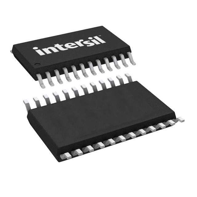
ICGOO电子元器件商城为您提供MAX3033EESE+由Maxim设计生产,在icgoo商城现货销售,并且可以通过原厂、代理商等渠道进行代购。 MAX3033EESE+价格参考。MaximMAX3033EESE+封装/规格:接口 - 驱动器,接收器,收发器, 驱动器 4/0 RS422,RS485 16-SO。您可以下载MAX3033EESE+参考资料、Datasheet数据手册功能说明书,资料中有MAX3033EESE+ 详细功能的应用电路图电压和使用方法及教程。
Maxim Integrated的MAX3033EESE+是一款高性能的RS-485/RS-422接口收发器,主要应用于工业自动化、通信设备、测试仪器等领域。该芯片支持半双工和全双工通信,具有高抗干扰能力和稳定的数据传输性能,适用于复杂电磁环境下的工业现场通信。其典型应用场景包括:

1. 工业自动化控制系统:用于PLC(可编程逻辑控制器)、DCS(分布式控制系统)和现场总线通信,实现设备间的可靠数据交换。
2. 楼宇自动化系统:如暖通空调(HVAC)、安防系统和智能照明控制,实现长距离、多点数据通信。
3. 电机驱动与机器人控制:用于工业机器人与控制器之间的高速、稳定通信。
4. 测试与测量设备:如示波器、信号发生器等仪器,用于与其他设备或计算机进行串口通信。
5. 交通运输系统:如列车控制系统、交通监控设备中的数据传输模块。

MAX3033EESE+具备宽电压供电范围(4.75V至5.25V),工作温度范围为-40°C至+85°C,适应工业级环境要求,是一款高可靠性的通信接口解决方案。
| 参数 | 数值 |
| 产品目录 | 集成电路 (IC)半导体 |
| 描述 | IC RS-422 TRANSMIT QUAD 16-SOICRS-422接口集成电路 3.3V Quad RS-422 ESD-Protected Trx |
| 产品分类 | |
| 品牌 | Maxim Integrated |
| 产品手册 | |
| 产品图片 |
|
| rohs | 符合RoHS无铅 / 符合限制有害物质指令(RoHS)规范要求 |
| 产品系列 | 接口 IC,RS-422接口集成电路,Maxim Integrated MAX3033EESE+- |
| 数据手册 | |
| 产品型号 | MAX3033EESE+ |
| 产品培训模块 | http://www.digikey.cn/PTM/IndividualPTM.page?site=cn&lang=zhs&ptm=25703http://www.digikey.cn/PTM/IndividualPTM.page?site=cn&lang=zhs&ptm=25705 |
| 产品目录页面 | |
| 产品种类 | RS-422接口集成电路 |
| 传播延迟时间ns | 16 ns |
| 供应商器件封装 | 16-SOIC |
| 关闭 | Yes |
| 功能 | Driver |
| 包装 | 管件 |
| 协议 | RS422 |
| 双工 | - |
| 商标 | Maxim Integrated |
| 安装类型 | 表面贴装 |
| 安装风格 | SMD/SMT |
| 封装 | Tube |
| 封装/外壳 | 16-SOIC(0.154",3.90mm 宽) |
| 封装/箱体 | SO-Narrow-16 |
| 工作温度 | -40°C ~ 85°C |
| 工作温度范围 | 0 C to + 70 C |
| 工作电源电压 | 3 V to 3.6 V |
| 工厂包装数量 | 50 |
| 接收器滞后 | - |
| 接收机数量 | 0 |
| 数据速率 | 2 Mbps |
| 最大功率耗散 | 696 mW |
| 最大工作温度 | + 85 C |
| 最小工作温度 | - 40 C |
| 标准包装 | 1 |
| 激励器数量 | 4 |
| 电压-电源 | 3 V ~ 3.6 V |
| 电源电流 | 100 uA |
| 类型 | 驱动器 |
| 系列 | MAX3033E |
| 输入电压 | 3.3 V |
| 输出电压 | 2 V to 3.6 V |
| 输出电流 | 20 uA |
| 零件号别名 | MAX3033E |
| 驱动器/接收器数 | 4/0 |


PDF Datasheet 数据手册内容提取
19-2671; Rev 0; 10/02 ±15kV ESD-Protected, 3.3V Quad RS-422 Transmitters General Description Features M The MAX3030E–MAX3033E family of quad RS-422 (cid:2) Meet TIA/EIA-422-B (RS-422) and ITU-T V.11 A transmitters send digital data transmission signals over Recommendation X twisted-pair balanced lines in accordance with TIA/EIA- 422-B and ITU-T V.11 standards. All transmitter outputs (cid:2) ±15kV ESD Protection on Tx Outputs 3 are protected to ±15kV using the Human Body Model. (cid:2) Hot-Swap Functionality 0 The MAX3030E–MAX3033E are available with either a 2Mbps or 20Mbps guaranteed baud rate. The 2Mbps (cid:2) Guaranteed 20Mbps Data Rate (MAX3030E, 3 0 baud rate transmitters feature slew-rate-limiting to mini- MAX3032E) mize EMI and reduce reflections caused by improperly (cid:2) Slew-Rate-Controlled 2Mbps Data Rate E terminated cables. – (MAX3031E, MAX3033E) M The 20Mbps baud rate transmitters feature low-static (cid:2) Available in 16-Pin TSSOP and Narrow SO current consumption (ICC < 100µA), making them ideal A for battery-powered and power-conscious applications. Packages They have a maximum propagation delay of 16ns and a (cid:2) Low-Power Design (<330µW, VCC= 3.3V Static) X part-to-part skew less than 5ns, making these devices 3 ideal for driving parallel data. The MAX3030E– (cid:2) +3.3V Operation 0 MAX3033E feature hot-swap capability that eliminates (cid:2) Industry-Standard Pinout 3 false transitions on the data cable during power-up or hot insertion. (cid:2) Thermal Shutdown 3 E The MAX3030E–MAX3033E are low-power, ESD-pro- tected, pin-compatible upgrades to the industry-stan- dard 26LS31 and SN75174. They are available in space-saving 16-pin TSSOP and SO packages. Applications Ordering Information Telecom Backplanes V.11/X.21 Interface PART TEMP RANGE PIN-PACKAGE MAX3030ECSE 0°C to +70°C 16 SO (Narrow) Industrial PLCs MAX3030ECUE 0°C to +70°C 16 TSSOP Motor Control MAX3030EESE -40°C to +85°C 16 SO (Narrow) MAX3030EEUE -40°C to +85°C 16 TSSOP MAX3031ECSE 0°C to +70°C 16 SO (Narrow) Pin Configurations MAX3031ECUE 0°C to +70°C 16 TSSOP MAX3031EESE -40°C to +85°C 16 SO (Narrow) TOP VIEW MAX3031EEUE -40°C to +85°C 16 TSSOP MAX3032ECSE 0°C to +70°C 16 SO (Narrow) DI1 1 16 VCC DI1 1 16 VCC MAX3032ECUE 0°C to +70°C 16 TSSOP DO1+ 2 15 DI4 DO1+ 2 15 DI4 MAX3032EESE -40°C to +85°C 16 SO (Narrow) DO1- 3 14 DO4+ DO1- 3 14 DO4+ EN 4 MAX3030E/ 13 DO4- EN1&2 4 MAX3032E/ 13 DO4- MAX3032EEUE -40°C to +85°C 16 TSSOP MAX3031E MAX3033E DO2- 5 12 EN DO2- 5 12 EN3&4 MAX3033ECSE 0°C to +70°C 16 SO (Narrow) DO2+ 6 11 DO3- DO2+ 6 11 DO3- MAX3033ECUE 0°C to +70°C 16 TSSOP DI2 7 10 DO3+ DI2 7 10 DO3+ MAX3033EESE -40°C to +85°C 16 SO (Narrow) GND 8 9 DI3 GND 8 9 DI3 MAX3033EEUE -40°C to +85°C 16 TSSOP TSSOP/SO TSSOP/SO ________________________________________________________________Maxim Integrated Products 1 For pricing, delivery, and ordering information,please contact Maxim/Dallas Direct!at 1-888-629-4642, or visit Maxim’s website at www.maxim-ic.com.
±15kV ESD-Protected, 3.3V Quad RS-422 Transmitters E ABSOLUTE MAXIMUM RATINGS 3 (All Voltages Are Referenced to Device Ground, Unless Continuous Power Dissipation (TA= +70°C) 3 Otherwise Noted) 16-Pin SO (derate 8.70mW/°C above +70°C)..............696mW 0 VCC........................................................................................+6V 16-Pin TSSOP (derate 9.40mW/°C above +70°C).......755mW EN1&2, EN3&4, EN, EN............................................-0.3V to +6V Operating Temperature Ranges 3 DI_............................................................................-0.3V to +6V MAX303_EC_......................................................0°C to +70°C X DO_+, DO_- (normal condition).................-0.3V to (VCC+ 0.3V) MAX303_EE_...................................................-40°C to +85°C DO_+, DO_- (power-off or three-state condition).....-0.3V to +6V Junction Temperature......................................................+150°C A Driver Output Current per Pin.........................................±150mA Storage Temperature Range.............................-65°C to +160°C M Lead Temperature (soldering, 10s).................................+300°C – Stresses beyond those listed under “Absolute Maximum Ratings” may cause permanent damage to the device. These are stress ratings only, and functional operation of the device at these or any other conditions beyond those indicated in the operational sections of the specifications is not implied. Exposure to E absolute maximum rating conditions for extended periods may affect device reliability. 0 3 DC ELECTRICAL CHARACTERISTICS 0 (3V ≤VCC≤3.6V, TA= TMINto TMAX, unless otherwise noted. Typical values are at VCC= +3.3V and TA= +25°C.) (Note 1) 3 X PARAMETER SYMBOL CONDITIONS MIN TYP MAX UNITS A DRIVER OUTPUT: DO_+, DO_- M VOD1 RL = 100Ω, Figure 1 2.0 VOD2 RL = ∞, Figure 1 3.6 Differential Driver Output V RL = 3.9kΩ (for compliance with V.11), VOD3 3.6 Figure 1 Change in Differential Output ∆VOD RL = 100Ω (Note 2) -0.4 +0.4 V Voltage Driver Common-Mode Output VOC RL = 100Ω, Figure 1 3 V Voltage Change in Common-Mode ∆VOC RL = 100Ω (Note 2) -0.4 +0.4 V Voltage Three-State Leakage Current IOZ VOUT = VCC or GND, driver disabled ±10 µA Output Leakage Current IOFF VCC = 0V, VOUT = 3V or 6V 20 µA Driver Output Short-Circuit VOUT = 0V, VIN = VCC or GND ISC -150 mA Current (Note 3) INPUTS: EN, EN, EN1&2, EN3&4 Input High Voltage VIH 2.0 V Input Low Voltage VIL 0.4 V Input Current ILEAK ±2 µA Hot-Swap Driver Input Current IHOTSWAP EN, EN, EN1&2, EN3&4 (Note 4) ±200 µA SUPPLY CURRENT Supply Current ICC No load 100 µA THERMAL PROTECTION Thermal-Shutdown Threshold TSH 160 °C Thermal-Shutdown Hysteresis 10 °C ESD Protection DO_ Human Body Model ±15 kV 2 _______________________________________________________________________________________
±15kV ESD-Protected, 3.3V Quad RS-422 Transmitters SWITCHING CHARACTERISTICS—MAX3030E, MAX3032E M (3V ≤VCC≤3.6V, TA= TMINto TMAX, unless otherwise noted. Typical values are at VCC= +3.3V and TA= +25°C.) A PARAMETER SYMBOL CONDITIONS MIN TYP MAX UNITS X Driver Propagation Delay 3 tDPLH Low to High 0 RL = 100Ω, CL = 50pF, Figures 2, 3 8 16 ns Driver Propagation Delay 3 tDPHL High to Low 0 Differential Transition Time, Low E tR to High RL = 100Ω, CL = 50pF (10% to 90%), – Differential Transition Time, High Figures 2, 3 10 ns M tF to Low A Differential Skew (Same Channel) X tSK1 |tDPLH - tDPHL| RL = 100Ω, CL = 50pF, VCC = 3.3V ±2 ns 3 Skew Driver to Driver 0 tSK2 (Same Device) 3 RL = 100Ω, CL = 50pF, VCC = 3.3V, 3 Skew Part to Part tSK3 ∆TMAX = +5°C 5 ns E Maximum Data Rate 20 Mbps S2 closed, RL = 500Ω, CL = 50pF, Driver Enable to Output High tDZH 50 ns Figures 4, 5 S1 closed, RL = 500Ω, CL = 50pF, Driver Enable to Output Low tDZL 50 ns Figures 4, 5 S1 closed, RL = 500Ω, CL = 50pF, Driver Disable Time from Low tDLZ 50 ns Figures 4, 5 S2 closed, RL = 500Ω, CL = 50pF, Driver Disable Time from High tDHZ 50 ns Figures 4, 5 SWITCHING CHARACTERISTICS—MAX3031E, MAX3033E (3V ≤VCC≤3.6V, TA= TMINto TMAX, unless otherwise noted. Typical values are at VCC= +3.3V and TA= +25°C.) PARAMETER SYMBOL CONDITIONS MIN TYP MAX UNITS Driver Propagation Delay tDPLH Low to High RL = 100Ω, CL = 50pF, Figures 2, 3 40 70 ns Driver Propagation Delay tDPHL High to Low Differential Transition Time, tR Low to High RL = 100Ω, CL = 50pF (10% to 90%), 15 50 ns Differential Transition Time, Figures 2, 3 tF High to Low Differential Skew (Same Channel) tSK1 |tDPLH - tDPHL| RL = 100Ω, CL = 50pF, VCC = 3.3V ±10 ns Skew Driver to Driver tSK2 (Same Device) _______________________________________________________________________________________ 3
±15kV ESD-Protected, 3.3V Quad RS-422 Transmitters E SWITCHING CHARACTERISTICS—MAX3031E, MAX3033E (continued) 3 (3V ≤VCC≤3.6V, TA= TMINto TMAX, unless otherwise noted. Typical values are at VCC= +3.3V and TA= +25°C.) 3 PARAMETER SYMBOL CONDITIONS MIN TYP MAX UNITS 0 3 Skew Part to Part tSK3 R∆TL M=A 1X0 =0 Ω+,5 C°CL = 50pF, VCC = 3.3V, 18 ns X Maximum Data Rate 2 Mbps A S2 closed, RL = 500Ω, CL = 50pF, M Driver Enable to Output High tDZH 100 ns Figures 4, 5 – S1 closed, RL = 500Ω, CL = 50pF, E Driver Enable to Output Low tDZL Figures 4, 5 100 ns 0 S1 closed, RL = 500Ω, CL = 50pF, 3 Driver Disable Time from Low tDLZ Figures 4, 5 150 ns 0 S2 closed, RL = 500Ω, CL = 50pF, 3 Driver Disable Time from High tDHZ 150 ns Figures 4, 5 X Note 1: All currents into the device are positive; all currents out of the device are negative. All voltages are referenced to device A ground, unless otherwise noted. M Note 2: ∆VODand ∆VOCare the changes in VODand VOC, respectively, when DI changes state. Note 3: Only one output shorted at a time. Note 4: This input current is for the hot-swap enable (EN_, EN, EN) inputs and is present until the first transition only. After the first transition, the input reverts to a standard high-impedance CMOS input with input current ILEAK. Typical Operating Characteristics (VCC= +3.3V and TA= +25°C, unless otherwise noted.) DIFFERENTIAL OUTPUT VOLTAGE OUTPUT CURRENT OUTPUT CURRENT vs. OUTPUT CURRENT vs. TRANSMITTER OUTPUT LOW VOLTAGE vs. TRANSMITTER OUTPUT HIGH VOLTAGE AL OUTPUT VOLTAGE (V) 234 TA = 0°C TA = +25°C MAX3030E toc01 UT CURRENT (mA) 112050000 MAX3030E toc02 UT CURRENT (mA) 11170255050 MAX3030E toc03 ERENTI 1 TA = +85°C OUTP 50 OUTP 50 F F DI 25 0 0 0 0 30 60 90 120 0 1 2 3 4 0 1 2 3 4 OUTPUT CURRENT (mA) OUTPUT LOW VOLTAGE (V) OUTPUT HIGH VOLTAGE (V) 4 _______________________________________________________________________________________
±15kV ESD-Protected, 3.3V Quad RS-422 Transmitters Typical Operating Characteristics (continued) M (VCC= +3.3V and TA= +25°C, unless otherwise noted.) A X SUPPLY CURRENT MAX3030E/MAX3032E MAX3031E/MAX3033E 3 vs. SUPPLY VOLTAGE SUPPLY CURRENT vs. DATA RATE SUPPLY CURRENT vs. DATA RATE µSUPPLY CURRENT (A) 146800000 DRIVERST AE N= A+B2L5E°TCDA = +85°C TA = 0°C MAX3030E toc04 SUPPLY CURRENT (mA) 1122305050 ATSNRLWOLA IR NTFECSOSHMUIISRINTTGTIVEER SLOAD, CL = 200pF, MAX3030E toc05 SUPPLY CURRENT (mA) 1122....0505 ATSNRLWOLA IR NTFECSOSHMUIISRINTTGTIVEER SLOAD, CL = 200pF, MAX3030E toc06 030E–MA X 20 0.5 5 3 0 0 0 0 0 1 2 3 4 0.1k 1k 10k 100k 1M 10M 100M 0.1k 1k 10k 100k 1M 10M 3 SUPPLY VOLTAGE (V) DATA RATE (bps) DATA RATE (bps) 3 MAX3030E E MAX3030E/MAX3032E MAX3031E/MAX3033E DRIVER PROPAGATION DELAY SUPPLY CURRENT vs. DATA RATE SUPPLY CURRENT vs. DATA RATE (LOW TO HIGH) 130 100 MAX3030E toc09 120 ALROLL LA= D F1OE0DU0 ΩRA N,T CRDAL S N=WS 2IMT0C0ITpHTFIENRGS MAX3030E toc07 ALROLL LA= D F1OE0DU0 ΩRA N,T CRDAL S N=WS 2IMT0C0ITpHTFIENRGS MAX3030E toc08 D1VI_/div A) A) 97 m m T ( T ( N 110 N E E R R UR UR 94 DIFFERENTIAL PLY C 100 PLY C O2VU/TdPivUT P P U U S S 91 90 80 88 0.1k 1k 10k 100k 1M 10M 100M 0.1k 1k 10k 100k 1M 10M 10ns/div DATA RATE (bps) DATA RATE (bps) MAX3030E MAX3031E MAX3031E DRIVER PROPAGATION DELAY DRIVER PROPAGATION DELAY DRIVER PROPAGATION DELAY (HIGH TO LOW) (LOW TO HIGH) (HIGH TO LOW) MAX3030E toc10 MAX3030E toc11 MAX3030E toc12 DI_ 1V/div DIFFERENTIAL OUTPUT DIFFERENTIAL DIFFERENTIAL 2V/div OUTPUT OUTPUT 2V/div 2V/div DI_ DI_ 1V/div 1V/div 10ns/div 20ns/div 20ns/div _______________________________________________________________________________________ 5
±15kV ESD-Protected, 3.3V Quad RS-422 Transmitters E Typical Operating Characteristics (continued) 3 (VCC= +3.3V and TA= +25°C, unless otherwise noted.) 3 0 ENABLE RESPONSE TIME MAX3033E EYE DIAGRAM 3 MAX3030E toc13 MAX3030E toc14 ENABLE X 1V/div A M DO_+ – DIFFERENTIAL 1V/div E OUTPUT 2V/div 0 DO_- 3 1V/div 0 3 X 20ns/div 100ns/div A M Pin Description PIN MAX3030E/ MAX3032E/ NAME FUNCTION MAX3031E MAX3033E Transmitter Inputs. When the corresponding transmitter is enabled, a low on DI_ forces DI1, DI2, 1, 7, 9, 15 1, 7, 9, 15 the noninverting output low and inverting output high. Similarly, a high on DI_ forces DI3, DI4 noninverting output high and inverting output low. DO1+, DO2+, 2, 6, 10, 14 2, 6, 10, 14 Noninverting RS-422 Outputs DO3+, DO4+ DO1-, DO2-, 3, 5, 11, 13 3, 5, 11, 13 Inverting RS-422 Outputs DO3-, DO4- Transmitter Enable Input: Active HIGH. Drive EN HIGH to enable all transmitters. When EN is HIGH, drive EN LOW to disable (three-state) all the transmitters. The transmitter 4 — EN outputs are high impedance when disabled. EN is hot-swap protected (see the Hot Swap section). 8 8 GND Ground Transmitter Enable Input: Active LOW. Drive EN LOW to enable all transmitters. When 12 — EN EN is LOW, drive EN HIGH to disable all the transmitters. The transmitter outputs are high impedance when disabled. EN is hot-swap protected (see the Hot Swap section). Transmitter Enable Input for Channels 1 and 2. Drive EN1&2 HIGH to enable the corresponding transmitters. Drive EN1&2 LOW to disable the corresponding — 4 EN1&2 transmitters. The transmitter outputs are high impedance when disabled. EN1&2 is hot- swap protected (see the Hot Swap section). Transmitter Enable Input for Channels 3 and 4. Drive EN3&4 HIGH to enable the corresponding transmitters. Drive EN3&4 LOW to disable the corresponding — 12 EN3&4 transmitters. The transmitter outputs are high impedance when disabled. EN3&4 is hot- swap protected (see the Hot Swap section). 16 16 VCC Positive Supply; +3V ≤ VCC ≤ +3.6V. Bypass VCC to GND with a 0.1µF capacitor. 6 _______________________________________________________________________________________
±15kV ESD-Protected, 3.3V Quad RS-422 Transmitters Test Circuits and Timing Diagrams M A CL X DI_+ DO_+ 3 RL 0 2 3 VOD VOC DI_ VOD RL CL 0 RL E 2 – DI_- DO_- M CL A X Figure 1. Differential Driver DC Test Circuit Figure 2. Differential Driver Propagation Delay and Transition 3 Time Test Circuit 0 3 3 3V E DI 1.5V 1.5V 0V tDPLH tDPHL 1/2 VO DO_- OUTPUT RL S1 VCC VO UNDER TEST DO_+ CL 1/2 VO S2 VDIFF = V (DO_+) - V (DO_-) VO VDIFF 0V 10% 90% 90% 10% ENABLE SIGNAL IS ONE OF THE POSSIBLE -VO ENABLE CONFIGURATIONS (SEE TRUTH TABLE). tR tF tSKEW = |tDPLH - tDPHL| Figure 3. Differential Driver Propagation Delay and Transition Figure 4. Driver Enable/Disable Delays Test Circuit Waveform 3V EN 1.5V 1.5V 0V tDZL tDLZ VCC DO_+ A VOL 1.5V OUTPUT NORMALLY LOW VOL + 0.3V DI GND A DO_- VOH OUTPUT NORMALLY HIGH 1.5V VOH - 0.3V 0V tDZH tDHZ ENABLE SIGNAL IS ONE OF THE POSSIBLE ENABLE CONFIGURATIONS (SEE TRUTH TABLE). Figure 5. Driver Enable/Disable Waveform Figure 6. Short-Circuit Measurements _______________________________________________________________________________________ 7
±15kV ESD-Protected, 3.3V Quad RS-422 Transmitters E Test Circuits and transmitter outputs of this product family are character- ized for protection to ±15kV using the Human Body 3 Timing Diagrams (continued) Model. Other ESD test methodologies include 3 IEC10004-2 Contact Discharge and IEC1000-4-2 Air- 0 Gap Discharge (formerly IEC801-2). 3 DO_+ VCC A ESD Test Conditions X DI ESD performance depends on a variety of conditions. A A GND DO_- Contact Maxim for a reliability report that documents M test setup, test methodology, and test results. Human Body Model – E Figure 8 shows the Human Body Model, and Figure 9 shows the current waveform it generates when dis- 0 Figure 7. Power-Off Measurements charged into low impedance. This model consists of a 3 Detailed Description 100pF capacitor charged to the ESD voltage of interest, 0 which is then discharged into the test device through a 3 The MAX3030E–MAX3033E are high-speed quad RS- 1.5kΩresistor. 422 transmitters designed for digital data transmission X over balanced lines. They are designed to meet the A requirements of TIA/EIA-422-B and ITU-T V.11. The M MAX3030E–MAX3033E are available in two pinouts to 1RMCΩ 1.R5DkΩ be compatible with both the 26LS31 and SN75174 industry-standard devices. Both are offered in 20Mbps CHARGE-CURRENT- DISCHARGE and 2Mbps baud rate. All versions feature a low-static LIMIT RESISTOR RESISTANCE current consumption (ICC < 100µA) that makes them ideal for battery-powered and power-conscious appli- HIGH- DEVICE VOLTAGE Cs STORAGE UNDER cations. The 20Mbps version has a maximum propaga- DC 100pF CAPACITOR TEST tion delay of 16ns and a part-to-part skew less than SOURCE 5ns, allowing these devices to drive parallel data. The 2Mbps version is slew-rate-limited to reduce EMI and reduce reflections caused by improperly terminated cables. Outputs have enhanced ESD protection providing Figure 8. Human Body ESD Test Model ±15kV tolerance. All parts feature hot-swap capability that eliminates false transitions on the data cable dur- ing power-up or hot insertion. ±15kV ESD Protection IP 100% Ir PEAK-TO-PEAK RINGING As with all Maxim devices, ESD-protection structures 90% (NOT DRAWN TO SCALE) are incorporated on all pins to protect against electro- static discharges encountered during handling and AMPS assembly. The driver outputs and receiver inputs have 36.8% extra protection against static electricity. Maxim’s engi- neers developed state-of-the-art structures to protect 10% these pins against ESD of ±15kV without damage. The 0 0 TIME ESD structures withstand high ESD in all states: normal tRL operation and power-down. After an ESD event, the tDL CURRENT WAVEFORM MAX3030E–MAX3033E keep working without latchup. ESD protection can be tested in various ways; the Figure 9. Human Body Current Waveform 8 _______________________________________________________________________________________
±15kV ESD-Protected, 3.3V Quad RS-422 Transmitters Machine Model M The Machine Model for ESD tests all pins using a 200pF storage capacitor and zero discharge resis- A VCC tance. Its objective is to emulate the stress caused by X contact that occurs with handling and assembly during 6µs 3 manufacturing. Of course, all pins require this protec- TIMER tion during manufacturing, not just inputs and outputs. 0 Therefore, after PC board assembly, the Machine 3 TIMER Model is less relevant to I/O ports. 0 Hot Swap E – When circuit boards are plugged into a “hot” back- M plane, there can be disturbances to the differential sig- nal levels that could be detected by receivers A connected to the transmission line. This erroneous data X could cause data errors to an RS-422 system. To avoid 5.6kΩ this, the MAX3030E–MAX3033E have hot-swap capa- EN DE 3 (HOT SWAP) ble inputs. 0 When a circuit board is plugged into a “hot” backplane, 100µA 2mA 3 there is an interval during which the processor is going M1 M2 3 through its power-up sequence. During this time, the E processor’s output drivers are high impedance and are unable to drive the enable inputs of the MAX3030E– MAX3033E (EN, EN, EN_) to defined logic levels. Figure 10. Simplified Structure of the Driver Enable Pin (EN) Leakage currents from these high-impedance drivers, of as much as 10µA, could cause the enable inputs of the MAX3030E–MAX3033E to drift high or low. 3.3V Additionally, parasitic capacitance of the circuit board could cause capacitive coupling of the enable inputs to VCC either GND or VCC. These factors could cause the 1kΩ enable inputs of the MAX3030E–MAX3033E to drift to DO_+ levels that may enable the transmitter outputs. To avoid this problem, the hot-swap input provides a method of DI_ 0.1kΩ 50pF holding the enable inputs of the MAX3030E–MAX3033E (VCC OR GND) in the disabled state as VCC ramps up. This hot-swap DO_- input is able to overcome the leakage currents and par- asitic capacitances that can pull the enable inputs to 1kΩ the enabled state. Hot-Swap Input Circuitry In the MAX3030E–MAX3033E, the enable inputs feature Figure 11. Differential Power-Up Glitch (Hot Swap) hot-swap capability. At the input there are two NMOS current. At this time the SR latch resets and M1 turns off. devices, M1 and M2 (Figure 10). When VCC is ramping When M1 turns off, EN reverts to a standard, high- up from zero, an internal 6µs timer turns on M2 and sets the SR latch, which also turns on M1. Transistors M2, a impedance CMOS input. Whenever VCC drops below 1V, the hot-swap input is reset. The EN1&2 and EN3&4 2mA current sink, and M1, a 100µA current sink, pull EN to GND through a 5.6kΩ resistor. M2 is designed to pull input structures are identical to the EN input. For the EN input, there is a complementary circuit employing two the EN input to the disabled state against an external parasitic capacitance of up to 100pF that is trying to PMOS devices pulling the ENinput to VCC. enable the EN input. After 6µs, the timer turns M2 off and Hot-Swap Line Transient M1 remains on, holding the EN input low against three- The circuit of Figure 11 shows a typical offset termina- state output leakages that might enable EN. M1 remains tion used to guarantee a greater than 200mV offset on until an external source overcomes the required input when a line is not driven. The 50pF capacitor repre- _______________________________________________________________________________________ 9
±15kV ESD-Protected, 3.3V Quad RS-422 Transmitters E sents the minimum parasitic capacitance that would The MAX3032E/MAX3033E are compatible with the exist in a typical application. In most cases, more SN75174. EN1&2 controls transmitters 1 and 2, and EN 3 capacitance exists in the system and reduces the mag- 3&4 controls transmitters 3 and 4 (dual enable). 3 nitude of the glitch. During a “hot-swap” event when the Typical Applications 0 driver is connected to the line and is powered up, the 3 driver must not cause the differential signal to drop The MAX3030E–MAX3033E offer optimum performance X below 200mV (Figures 12 and 13). when used with the MAX3094E/MAX3096 3.3V quad differential line receivers. Figure 14 shows a typical RS- A Operation of Enable Pins 422 connection for transmitting and receiving data. M The MAX3030E–MAX3033E family has two enable-func- tional versions. – E The MAX3030E/MAX3031E are compatible with 26LS31, where the two enable signals control all four 0 transmitters (global enable). 3 0 3 X VCC VCC 1V/div 1V/div A M DO_+ - DO_- DO_+ - DO_- DO_+ DO_+ DO_- DO_- 4µs/div 1.0µs/div Figure 12. Differential Power-Up Glitch (0.1V/µs) Figure 13. Differential Power-Up Glitch (1V/µs) Table 1. MAX3030E/MAX3031E Transmitter Controls EN EN TX1 TX2 TX3 TX4 MODE 0 0 Active Active Active Active All transmitters active 0 1 High-Z High-Z High-Z High-Z All transmitters disabled 1 0 Active Active Active Active All transmitters active 1 1 Active Active Active Active All transmitters active Table 2. MAX3032E/MAX3033E Transmitter Controls EN1&2 EN3&4 TX1 TX2 TX3 TX4 MODE 0 0 High-Z High-Z High-Z High-Z All transmitters disabled 0 1 High-Z High-Z Active Active Tx 3 and 4 active 1 0 Active Active High-Z High-Z Tx 1 and 2 active 1 1 Active Active Active Active All transmitters active 10 ______________________________________________________________________________________
±15kV ESD-Protected, 3.3V Quad RS-422 Transmitters M MAX3030E/MAX3031E MAX3094 A X 3 DI1 D1 RT R1 R1OUT 0 3 0 E – M DI2 D2 RT R2 R2OUT A X 3 0 3 DI3 D3 RT R3 R3OUT 3 E DI4 D4 RT R4 R4OUT EN G EN G VCC GND VCC GND Figure 14. Typical Connection of a Quad Transmitter and Quad Receiver as a Pair ______________________________________________________________________________________ 11
±15kV ESD-Protected, 3.3V Quad RS-422 Transmitters E VCC GND 3 VCC GND 3 0 3 EN EN1&2 X EN EN3&4 A DO1+ M DI1 DO1- DO1+ DI1 – DO1- E 0 DO2+ DI2 3 DO2- DO2+ DI2 0 DO2- 3 X DI3 DO3+ DO3- DO3+ A DI3 DO3- M DO4+ DI4 DO4- DO4+ DI4 DO4- MAX3030E/MAX3031E MAX3032E/MAX3033E Figure 15. MAX3030E/MAX3031E Functional Diagram Figure 16. MAX3032E/MAX3033E Functional Diagram Chip Information TRANSISTOR COUNT: 1050 PROCESS: BiCMOS 12 ______________________________________________________________________________________
±15kV ESD-Protected, 3.3V Quad RS-422 Transmitters Package Information M (The package drawing(s) in this data sheet may not reflect the most current specifications. For the latest package outline information, A go to www.maxim-ic.com/packages.) X S 3 P E INCHES MILLIMETERS CN . 0 DIM MIN MAX MIN MAX SOI 3 A 0.053 0.069 1.35 1.75 0 N A1 0.004 0.010 0.10 0.25 B 0.014 0.019 0.35 0.49 E C 0.007 0.010 0.19 0.25 – e 0.050 BSC 1.27 BSC M E 0.150 0.157 3.80 4.00 E H H 0.228 0.244 5.80 6.20 A L 0.016 0.050 0.40 1.27 X VARIATIONS: 3 1 INCHES MILLIMETERS 0 TOP VIEW DIM MIN MAX MIN MAX N MS012 3 D 0.189 0.197 4.80 5.00 8 AA D 0.337 0.344 8.55 8.75 14 AB 3 D 0.386 0.394 9.80 10.00 16 AC E D C A e B A1 0 -8 L FRONT VIEW SIDE VIEW PROPRIETARY INFORMATION TITLE: PACKAGE OUTLINE, .150" SOIC APPROVAL DOCUMENT CONTROL NO. REV. 1 21-0041 B 1 ______________________________________________________________________________________ 13
±15kV ESD-Protected, 3.3V Quad RS-422 Transmitters E Package Information (continued) 3 (The package drawing(s) in this data sheet may not reflect the most current specifications. For the latest package outline information, go to www.maxim-ic.com/packages.) 3 0 S 3 P E m. X m 0 4 A 4. P O S M S T – E 0 3 0 3 X A M Maxim cannot assume responsibility for use of any circuitry other than circuitry entirely embodied in a Maxim product. No circuit patent licenses are implied. Maxim reserves the right to change the circuitry and specifications without notice at any time. 14 ____________________Maxim Integrated Products, 120 San Gabriel Drive, Sunnyvale, CA 94086 408-737-7600 © 2002 Maxim Integrated Products Printed USA is a registered trademark of Maxim Integrated Products.
Mouser Electronics Authorized Distributor Click to View Pricing, Inventory, Delivery & Lifecycle Information: M axim Integrated: MAX3030ECUE+ MAX3030EEUE+ MAX3031ECUE+T MAX3031EEUE+ MAX3032ECUE+ MAX3032EEUE+ MAX3032ECUE+G071 MAX3032ECUE+TG071 MAX3030ECSE+ MAX3030ECSE+T MAX3030ECUE+T MAX3030EESE+ MAX3030EESE+T MAX3030EEUE+T MAX3031ECSE+ MAX3031ECSE+T MAX3031ECUE+ MAX3031EESE+ MAX3031EESE+T MAX3031EEUE+T MAX3032ECSE+ MAX3032ECSE+T MAX3032ECUE+T MAX3032EESE+ MAX3032EESE+T MAX3032EEUE+T MAX3033ECSE+ MAX3033ECSE+T MAX3033ECUE+ MAX3033ECUE+T MAX3033EESE+ MAX3033EESE+T MAX3033EEUE+ MAX3033EEUE+T MAX3033EEUE