ICGOO在线商城 > 集成电路(IC) > PMIC - 稳压器 - 线性 > MAX1735EUK30+T

 Datasheet下载
- 型号: MAX1735EUK30+T
- 制造商: Maxim
- 库位|库存: xxxx|xxxx
- 要求:
| 数量阶梯 | 香港交货 | 国内含税 |
| +xxxx | $xxxx | ¥xxxx |
查看当月历史价格
查看今年历史价格
MAX1735EUK30+T产品简介:
ICGOO电子元器件商城为您提供MAX1735EUK30+T由Maxim设计生产,在icgoo商城现货销售,并且可以通过原厂、代理商等渠道进行代购。 MAX1735EUK30+T价格参考。MaximMAX1735EUK30+T封装/规格:PMIC - 稳压器 - 线性, Linear Voltage Regulator IC Negative Fixed or Adjustable 1 Output -3V, -1.25 V ~ -5.5 V 200mA SOT-23-5。您可以下载MAX1735EUK30+T参考资料、Datasheet数据手册功能说明书,资料中有MAX1735EUK30+T 详细功能的应用电路图电压和使用方法及教程。
MAX1735EUK30+T 是 Maxim Integrated 公司生产的一款 PMIC(电源管理集成电路),属于线性稳压器类别。该型号的应用场景主要包括以下几个方面:

1. 便携式设备:MAX1735 适合用于对功耗敏感的便携式设备,例如手持终端、PDA、智能手机和平板电脑等。其低静态电流和高效率特性能够延长电池续航时间。

2. 通信设备:适用于各种通信模块,如无线传感器网络节点、蓝牙模块和Wi-Fi模块。它能够为这些设备提供稳定的工作电压,确保信号传输的可靠性。

3. 工业自动化:在工业控制领域,MAX1735 可以为微控制器、数据采集系统和其他低功耗组件供电。其宽输入电压范围(2.7V 至 5.5V)适应多种电源环境。

4. 消费类电子产品:包括数码相机、MP3 播放器和个人健康监测设备(如智能手环)。MAX1735 的小尺寸封装(如 UK30 封装)使其非常适合空间受限的设计。

5. 医疗电子:可用于便携式医疗设备,如血糖仪、脉搏血氧仪和可穿戴健康监测器。其低噪声输出有助于提高传感器和信号处理电路的精度。

6. 物联网 (IoT) 设备:MAX1735 的高效能和紧凑设计使其成为 IoT 设备的理想选择,特别是那些依赖电池供电的节点设备。

这款线性稳压器具有以下关键特性,支持上述应用场景:
- 输出电压固定为 1.8V,最大输出电流可达 300mA;
- 高 PSRR(电源抑制比)以减少噪声干扰;
- 内置短路保护和过热关断功能,提升系统可靠性;
- 简化的外部元件需求,降低整体解决方案成本。

总之,MAX1735EUK30+T 在需要高效、稳定且小型化电源管理方案的场合中表现出色,特别适合低功耗和电池供电的应用环境。
| 参数 | 数值 |
| 产品目录 | 集成电路 (IC)半导体 |
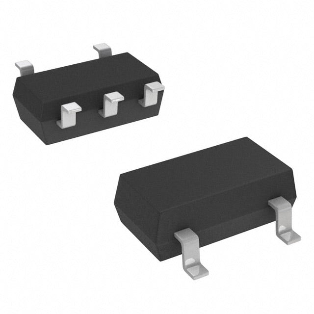
| 描述 | IC REG LDO -3/ADJ 0.2A SOT23-5低压差稳压器 200mA Negative Output |
| DevelopmentKit | MAXREFDES18# |
| 产品分类 | |
| 品牌 | Maxim Integrated |
| 产品手册 | |
| 产品图片 |
|
| rohs | 符合RoHS无铅 / 符合限制有害物质指令(RoHS)规范要求 |
| 产品系列 | 电源管理 IC,低压差稳压器,Maxim Integrated MAX1735EUK30+T- |
| 数据手册 | 点击此处下载产品Datasheet点击此处下载产品Datasheet点击此处下载产品Datasheet点击此处下载产品Datasheet |
| 产品型号 | MAX1735EUK30+T |
| 产品培训模块 | http://www.digikey.cn/PTM/IndividualPTM.page?site=cn&lang=zhs&ptm=25703http://www.digikey.cn/PTM/IndividualPTM.page?site=cn&lang=zhs&ptm=25705 |
| 产品种类 | 低压差稳压器 |
| 供应商器件封装 | SOT-23-5 |
| 其它名称 | MAX1735EUK30+TCT |
| 包装 | 剪切带 (CT) |
| 参考电压 | - 1.25 V |
| 商标 | Maxim Integrated |
| 回动电压—最大值 | 240 mV at - 200 mA |
| 安装类型 | 表面贴装 |
| 安装风格 | SMD/SMT |
| 封装 | Reel |
| 封装/外壳 | SC-74A,SOT-753 |
| 封装/箱体 | SOT-23 |
| 工作温度 | -40°C ~ 85°C |
| 工厂包装数量 | 2500 |
| 应用说明 | 点击此处下载产品Datasheet点击此处下载产品Datasheet点击此处下载产品Datasheet点击此处下载产品Datasheet点击此处下载产品Datasheet点击此处下载产品Datasheet点击此处下载产品Datasheet点击此处下载产品Datasheet点击此处下载产品Datasheet |
| 最大功率耗散 | 0.571 W |
| 最大工作温度 | + 85 C |
| 最大输入电压 | - 6.5 V |
| 最小工作温度 | - 40 C |
| 最小输入电压 | - 2.5 V |
| 标准包装 | 1 |
| 电压-跌落(典型值) | 0.08V @ 200mA |
| 电压-输入 | -2.5 V ~ -6.5 V |
| 电压-输出 | -3V,-1.25 V ~ -5.5 V |
| 电压调节准确度 | 1 % |
| 电流-输出 | 200mA |
| 电流-限制(最小值) | 1.02A |
| 稳压器拓扑 | 负固定式或可调式 |
| 稳压器数 | 1 |
| 系列 | MAX1735 |
| 线路调整率 | 0 % / V |
| 负载调节 | 0.004 % / mA |
| 输入偏压电流—最大 | 0.085 mA |
| 输出电压 | - 3 V/- 1.25 V to - 5.5 V |
| 输出电流 | 200 mA |
| 输出端数量 | 1 Output |
| 输出类型 | Adjustable, Fixed |
| 配用 | /product-detail/zh/MAXREFDES18%23/MAXREFDES18%23-ND/4441098/product-detail/zh/MAXREFDES6%23/MAXREFDES6%23-ND/4441097/product-detail/zh/MAXREFDES11%23/MAXREFDES11%23-ND/3877643 |
| 零件号别名 | MAX1735 |


PDF Datasheet 数据手册内容提取
19-1783; Rev 1; 11/03 200mA, Negative-Output, Low-Dropout Linear Regulator in SOT23 General Description Features M The MAX1735 negative-output, low-dropout linear regu- (cid:2) Guaranteed 200mA Output Current A lator operates from a -2.5V to -6.5V input and delivers a guaranteed 200mA with a low 80mV dropout. The high- (cid:2) Low 80mV Dropout Voltage at 200mA X accuracy (±1%) output voltage is preset or can be (cid:2) Low 85µA Quiescent Supply Current 1 adjusted from -1.25V to -5.5V with an external resistive 7 voltage-divider. (cid:2) Low 1nA Current Shutdown Mode 3 An internal N-channel MOSFET allows for a low 85µA (cid:2) Stable with 1µF COUT 5 quiescent current virtually independent of the load, (cid:2) PSRR >60dB at 100Hz making this device ideal for battery-powered portable equipment, such as PDAs, mobile phones, cordless (cid:2) Thermal Overload Protection phones, and wireless data modems. (cid:2) Short-Circuit Protection The device is available in several preset output voltage (cid:2) -5.0V, -3.0V, or -2.5V Output Voltage versions: -5.0V, -3.0V, and -2.5V. All versions offer a 1nA low-power shutdown mode, short-circuit protec- or Adjustable (-1.25V to -5.5V) tion, and thermal overload protection. The device is (cid:2) Tiny SOT23-5 Package offered in a tiny 5-pin SOT23 package. Applications Ordering Information Disk Drives PIN- PART TEMP RANGE Modems PACKAGE Instrumentation Amplifiers MAX1735EUK50-T -40°C to +85°C 5 SOT23-5 Notebook Computers MAX1735EUK30-T -40°C to +85°C 5 SOT23-5 MAX1735EUK25-T -40°C to +85°C 5 SOT23-5 Mobile and Cordless Telephones PCMCIA Cards GaAsFET Bias Output-Voltage Selector Guide Mobile Wireless Data Modems PRESET OUTPUT SOT TOP PART PDAs and Palmtop Computers VOLTAGE MARK MAX1735EUK50-T -5.0V or adj ADOZ MAX1735EUK30-T -3.0V or adj ADOY MAX1735EUK25-T -2.5V or adj ADOX Typical Operating Circuit Pin Configuration -5V, -3V, OR -2.5V TOP VIEW -6.5V TO -2.5V OUTPUT INPUT UP TO 200mA IN OUT GND 1 5 OUT CIN COUT MAX1735 MAX1735 IN 2 ON GND OFF SHDN SET ON SHDN 3 4 SET GND SOT23-5 ________________________________________________________________Maxim Integrated Products 1 For pricing, delivery, and ordering information,please contact Maxim/Dallas Direct!at 1-888-629-4642, or visit Maxim’s website at www.maxim-ic.com.
200mA, Negative-Output, Low-Dropout Linear Regulator in SOT23 5 ABSOLUTE MAXIMUM RATINGS 3 IN, SET to GND ....................................................-7.0V to +0.3V Operating Temperature Range...........................-40°C to +85°C 7 SOHUDTN tot oG GNNDD . ..........................................................................................((VVIINN-- 00..33))VV ttoo ++70..03VV JSutonrcatgioen T Teemmppeerraatuturree R..a..n..g...e...........................................................-.6..5..°..C... .t.o.. ++115500°°CC 1 Output Short-Circuit Duration........................................Indefinite Lead Temperature (soldering, 10s)................................+300°C X Continuous Power Dissipation (TA= +70°C) 5-Pin SOT23 (derate 7.1mW/°C above +70°C)...........571mW A Stresses beyond those listed under “Absolute Maximum Ratings” may cause permanent damage to the device. These are stress ratings only, and functional operation of the device at these or any other conditions beyond those indicated in the operational sections of the specifications is not implied. Exposure to M absolute maximum rating conditions for extended periods may affect device reliability. ELECTRICAL CHARACTERISTICS (Circuit of Figure 2, VIN= VOUT- 1V, VSHDN= VIN, TA= -40°C to +85°C, unless otherwise noted. Typical values are at TA= +25°C.) (Note 1) PARAMETER SYMBOL CONDITIONS MIN TYP MAX UNITS Input Voltage VIN -6.5 -2.5 V TA = +25°C, IOUT = -100µA -1 +1 Output Voltage Accuracy IOUT = -100µA, TA = 0°C to +85°C -2 +2 % ILOAD = -100µA to -200mA -3 +2 Circuit of Figure 3, TA = +25°C, IOUT = -100µA -1.2625 -1.25 -1.2375 Circuit of Figure 3, IOUT = -100µA, SET Regulation Set Point -1.275 -1.225 V TA = 0°C to +85°C Circuit of Figure 3, ILOAD = -100µA to -200mA -1.275 -1.2125 Maximum Output Current IOUT -200 mA Current Limit ILIM VOUT = 0 -1020 -515 -250 mA IOUT = -100µA -180 -85 Ground-Pin Current IQ µA IOUT = -200mA -125 IOUT = -100mA 40 Dropout Voltage (Note 2) mV IOUT = -200mA 80 240 Circuit of Figure 3, Line Regulation -0.15 0 +0.15 %/V VIN from -6.5V to -2.5V, VOUT = -1.25V Load Regulation IOUT from 0mA to -200mA 0.004 %/mA Output Voltage Noise 10Hz to 1MHz, COUT = 1µF 160 µVRMS Power-Supply Rejection Ratio PSRR f = 100Hz 60 dB TA = +25°C -1 -0.001 Shutdown Supply Current V SHDN = 0 TA = +85°C -1 µA SHDN Input High Threshold Positive voltage at SHDN +1.6 V (Note 3) Negative voltage at SHDN -1.6 SHDN Input Low Threshold Positive voltage at SHDN +0.4 V (Note 3) Negative voltage at SHDN -0.4 Set Input Bias Current ISET VSET = -1.25V, TA = +25°C -100 -15 nA SHDN Input Bias Current TA = +25°C V SHDN = +6.5V 3.5 µA V SHDN = 0, -6.5V -0.5 +0.5 Thermal Shutdown Junction Hysteresis = 15°C (typ) 160 °C Temperature Note 1: Limits are 100% production tested at TA= +25°C. Limits over operating temperature range are guaranteed by design. Note 2: The dropout voltage is defined as VOUT- VIN, when VOUTis 100mV above the nominal value of VOUT. Note 3: The SHDNlogic input can be driven by either a positive voltage or a negative voltage. | VSHDN| < 0.4V puts the device in shutdown, while | VSHDN| > 1.6V enables the device. 2 _______________________________________________________________________________________
200mA, Negative-Output, Low-Dropout Linear Regulator in SOT23 Typical Operating Characteristics M (Circuit of Figure 2, VIN= -4.0V, VOUT= -3.0V, TA= +25°C, unless otherwise specified.) A X SUPPLY CURRENT SUPPLY CURRENT vs. SUPPLY VOLTAGE vs. LOAD CURRENT 1 111648000 ILOAD = 200mA MAX1735 toc01 113400 MAX1735 toc02 735 µNT (A) 120 µNT (A) 120 URRE 100 URRE 110 SUPPLY C 8600 SUPPLY C 19000 40 80 20 0 70 0 -1 -2 -3 -4 -5 -6 -7 0 20 40 60 80 100 120 140 160 180 200 SUPPLY VOLTAGE (V) LOAD CURRENT (mA) SUPPLY CURRENT DROPOUT VOLTAGE vs. TEMPERATURE vs. LOAD CURRENT 111648000 ILOAD = 200mA MAX1735 toc03 18000 VOUT = -2.9V MAX1735 toc04 µSUPPLY CURRENT (A) 1186020000 NO LOAD DROPOUT VOLTAGE (mV) 6400 TA = +85°C TA = +25°CTA = -40°C 40 20 20 0 0 -40 -15 10 35 60 85 0 25 50 75 100 125 150 175 200 TEMPERATURE (°C) LOAD CURRENT (mA) OUTPUT VOLTAGE CHANGE OUTPUT VOLTAGE CHANGE vs. LOAD CURRENT vs. TEMPERATURE %) -0.02 VOUT = -3V MAX1735 toc05 %) 01..7050 MAX1735 toc06 HANGE ( -0.4 HANGE ( 00..2550 ILOAD = 200mA C C OLTAGE -0.6 TA = +85°C TA = -40°C OLTAGE 0 UT V -0.8 TA = +25°C UT V-0.25 NO LOAD P P UT UT-0.50 O O -1.0 -0.75 -1.2 -1.00 0 25 50 75 100 125 150 175 200 -40 -15 10 35 60 85 LOAD CURRENT (mA) TEMPERATURE (°C) _______________________________________________________________________________________ 3
200mA, Negative-Output, Low-Dropout Linear Regulator in SOT23 5 Typical Operating Characteristics (continued) 3 (Circuit of Figure 2, VIN= -4.0V, VOUT= -3.0V, TA= +25°C, unless otherwise specified.) 7 1 POWER-SUPPLY REJECTION RATIO OUTPUT NOISE DENSITY OUTPUT NOISE X vs. FREQUENCY vs. FREQUENCY (10Hz TO 1MHz) MA 6700 MAX1735 toc07 Hz) 10 MAX1735 toc08 5CIL0OO0UAµDT V ==/ d15iµ0vmFA MAX1735 toc09 PSRR (dB) 435000 COUT = 10µF µ√NOISE (V/RMS 1 T PU 0.1 20 COUT = 1.0µF UT O 10 0 0.01 1 10 100 1k 10k 100k 1M 10 1k 100k TIME (1ms/div) FREQUENCY (Hz) FREQUENCY (Hz) REGION OF STABLE ESR vs. LOAD CURRENT LINE-TRANSIENT RESPONSE 100 MAX1735 toc11 Ω ()UT 10 COUT = 1µF MAX1735 toc10 O R C VOUT ES 1 50mV/div E L B A T F S 0.1 ON O REGION OF STABILITY V1VIN/div GI E0.01 R 0.001 0 20 40 60 80 100 120 140 160 180 200 TIME (100µs/div) LOAD CURRENT (mA) LOAD-TRANSIENT RESPONSE LOAD-TRANSIENT RESPONSE (NORMAL OPERATION) (NEAR DROPOUT) MAX1735 toc12 MAX1735 toc13 ILOAD STEP ILOAD STEP 0 to 50mA 0 to 50mA VOUT VOUT 10mV/div 10mV/div TIME (100µs/div) TIME (100µs/div) 4 _______________________________________________________________________________________
200mA, Negative-Output, Low-Dropout Linear Regulator in SOT23 Typical Operating Characteristics (continued) M (Circuit of Figure 2, VIN= -4.0V, VOUT= -3.0V, TA= +25°C, unless otherwise specified.) A SHUTDOWN RESPONSE SHUTDOWN RESPONSE SHUTDOWN-PIN BIAS CURRENT X (DRIVEN FROM A POSITIVE VOLTAGE) (DRIVEN BY A NEGATIVE VOLTAGE) vs. SHUTDOWN-PIN VOLTAGE 1 MAX1735 toc14a MAX1735 toc14b 2.0 V200VSH/dDiNv 00V2VSH/dDiNv µN-PIN BIAS CURRENT (A) 011...505 LID LOGIC VOLTAGE LID LOGIC VOLTAGE MAX1735 toc15 735 V2VO/UdTiv V2VO/UdTiv TDOW INVA INVA U 0 H S -0.5 TIME (200µs/div) TIME (200µs/div) -6.5 -5.0 -3.5 -2.0 -0.5 1.0 2.5 4.0 5.5 SHUTDOWN-PIN VOLTAGE (V) Pin Description PIN NAME FUNCTION 1 GND Ground Regulator Input. Supply voltage can range from -2.5V to -6.5V. Bypass with a 1µF capacitor to GND 2 IN (see Capacitor Selection and Regulator Stability). This pin also functions as a heatsink. Solder to a large PC board pad or directly to the PC board power plane to maximize thermal dissipation. Shutdown Input. Drive SHDN to GND to turn the regulator off, reducing the input current to less than 3 SHDN 1nA. Drive SHDN above +1.6V or below -1.6V to enable the regulator. Connect SHDN to IN for always-on operation. Dual Mode™ Regulator Feedback Input. Connect SET to GND for the preset output voltage. Use a 4 SET resistive voltage-divider from OUT to SET to set the output voltage between -1.25V and -5.5V. Regulation setpoint is -1.25V. Regulator Output. OUT supplies up to 200mA in regulation. Bypass to GND with a 1µF ceramic 5 OUT capacitor. Dual Mode is a trademark of Maxim Integrated Products, Inc. _______________________________________________________________________________________ 5
200mA, Negative-Output, Low-Dropout Linear Regulator in SOT23 5 3 IN 7 THERMAL 1 CIN SENSOR NMOS PASS X SHUTDOWN TRANSISTOR A LOGIC OUT M ON SHDN GND OFF MAX1735 ON COUT ERROR AMPLIFIER R1 VREF -1.25V SET Dual Mode COMPARATOR R2 -270mV GND Figure 1. Functional Diagram Detailed Description comparator selects the feedback path based on VSET. Connect SET to GND to use the internal feedback path, The MAX1735 is a low-dropout negative linear voltage setting the output voltage to the preset value. If an regulator. It features Dual Mode operation, allowing a external voltage-divider is used, see Output Voltage fixed -5.0V, -3.0V, or -2.5V output voltage or an Selection. adjustable output from -1.25V to -5.5V. The regulator is guaranteed to supply 200mA of output current. It fea- Internal N-Channel MOSFET tures 60dB power-supply rejection for noise-sensitive The MAX1735 features an N-channel MOSFET pass applications and a low 85µA operating current that opti- transistor. Unlike similar designs using NPN bipolar mizes it for battery-operated devices. pass transistors, N-channel MOSFETs require extreme- As Figure 1 illustrates, the device consists of an internal ly low drive currents, reducing overall quiescent cur- -1.25V reference, an error amplifier, an N-channel rent. Also, NPN-based regulators consume still more MOSFET, an internal precision-trimmed feedback volt- base current in dropout conditions when the pass tran- age-divider, and a Dual Mode comparator. sistor saturates. The MAX1735 does not suffer from these problems, consuming only 125µA total current at The -1.25V reference is connected to the inverting input full load and in dropout. of the error amplifier. The error amplifier compares the reference voltage with the selected feedback voltage Output Voltage Selection and amplifies the difference. The error amplifier drives The MAX1735 features Dual Mode operation, allowing for the MOSFET to control the output voltage. a preset or adjustable output voltage. In preset voltage The feedback voltage for regulation is generated by mode, the output of the MAX1735 is set to -5.0V, -3.0V, or either an internal or external resistive voltage-divider -2.5V (see Ordering Information). Select this mode by connected from OUT to SET. The internal Dual Mode connecting SET to GND (Figure 2). 6 _______________________________________________________________________________________
200mA, Negative-Output, Low-Dropout Linear Regulator in SOT23 M -5.5V TO -1.25V -6.5V TO -2.5V F-5IX.0EVD,-3.0V, OR -2.5V -6.5VIN TPOU -T2.5V AODUJTUPSUTTABLE A INPUT OUTPUT IN OUT X IN OUT CIN COUT 1µF CERAMCIICN C1µOUF TCERAMIC 1µF CERAMIC R1 1CµERF AMIC 1 MAX1735 7 MAX1735 ON 3 ON GND OFF SHDN SET 5 GND OFF SHDN SET ON ON GND GND R2 VOUT = VSET(1 + R1) R2 Figure 2. Typical Application Circuit with Preset Output Voltage Figure 3. Typical Application Circuit with Adjustable Output Voltage In adjustable mode, an output voltage between -5.5V and -1.25V is selected using two external resistors connected Current Limiting as a voltage-divider from OUT to SET (Figure 3). The out- The MAX1735 features a current limit that protects the put voltage is determined by the following equation: regulator. Short-circuit output current is typically 515mA. The output will withstand a short to ground V =V 1+R1 indefinitely; however, if the increased power dissipation OUT SET R2 heats the die to +160°C, the thermal overload protec- tion will shut off the regulator, preventing damage to the where VSET= VREFERENCE= -1.25V when in regulation. IC. Since the input bias current at SET is <100nA, use large resistance values for R1 and R2 to minimize Thermal Overload Protection power consumption in the feedback network. A typical The thermal overload protection circuit protects the reg- value of 100kΩ for R2 is acceptable for most applica- ulator against overheating due to prolonged overload tions. Higher values consume less current at the conditions. When the die temperature exceeds +160°C, expense of output voltage accuracy. The above equa- an on-chip thermal sensor disables the pass transistor, tion solved for R1 is: allowing the IC to cool. The thermal sensor reenables the pass MOSFET once the die temperature drops V 15°C. A continuous short-circuit fault condition results in R1=R2 OUT−1 VSET a cyclical enabling and disabling of the output. Thermal overload protection is designed to safeguard For preset output voltage mode, connect SET directly the MAX1735 in the event of overload fault conditions. to GND. For normal operation, do not exceed the absolute maxi- mum junction temperature rating of +150°C. Junction Shutdown temperature is greater than ambient by an amount In shutdown, the N-channel MOSFET, control circuitry, depending on package heat dissipation and the ther- reference, and all internal circuits are turned off, reduc- mal resistance from the junction to ambient (θJA): ing supply current to typically 1nA. SHDN can be dri- TJUNCTION= TAMBIENT + (θJA)(PDISSIPATION) ven by either a positive or negative voltage. Drive SHDN above +1.6V or below -1.6V to turn the regulator where on. To turn the regulator off, drive SHDN to GND. For θJA for the 5-pin SOT23 is about 0.140°C/mW. always-on operation, connect SHDNto IN. By including a positive threshold at SHDN, it can be driven by a standard 5V TTL level without needing level-shifting cir- cuitry. _______________________________________________________________________________________ 7
200mA, Negative-Output, Low-Dropout Linear Regulator in SOT23 5 selected ambient temperatures. The working principle is MAXIMUM OUTPUT CURRENT that the SOT23-5 package is small enough that in a typi- 3 vs. INPUT-OUTPUT VOLTAGE DIFFERENTIAL cal application circuit at room temperature, the package 7 250 GE cannot dissipate enough power to allow -6.5V to be reg- MAX1 MAXIMUM OUTPUT CURRENT (mA) 12155000000 DEVICE IN DROPOUTMAXIAJ(MTUTJU N M=MC A+T C1XIO5OIM0NN°U TTCIMEN)MUTAOP =UT +AS8 5=C T°+ACU7 0=R °+CR5E0N°CT UPPLY VOLTAGE – MIN OUTPUT VOLTA uApTlhasae ttiaeo emdnq btuinoiaec t-nri1oet. na2te s5f|omeVIOrs p atUhettoT er- a |2aft=au0llmor0PewmMi| lVy fAAafO ooX llUorfs −uT,ca tTu t−phgArθVuverJI−tee N Aaas7(m|v t0feaooril lrlaeoob pwtlheesar :apnto in1wg2e 0rr0e dmgiisWosn)i-.. S AX where |IOUT| is in mA, |VOUT - VIN| in V, PMAX (571mW) M 0 is the absolute maximum rated power dissipation at 0 1 2 3 4 5 6 +70°C for the SOT23-5, and θJA (0.140°C/mW) is the INPUT-OUTPUT VOLTAGE DIFFERENTIAL (V) approximate junction-to-ambient thermal resistance of the SOT23-5 in a typical application. Figure 4. Output Current and In-Out Voltage Differential Operating Region Bounded by Available Power Dissipation at A key to reducing θCA, thereby increasing thermal con- Selected Ambient Temperatures ductivity to the PC board, is to provide large PC board pads and traces for IN. Operating Region and Power Dissipation __________Applications Information Maximum power dissipation of the MAX1735 depends on the thermal resistance of the case and the circuit Capacitor Selection and board, the temperature difference between the die Regulator Stability junction and ambient air, and the rate of air flow (see Capacitors are required at the input and output of the also Thermal Overload Protection). The maximum MAX1735. Connect a 1µF or greater capacitor between power that can be dissipated by the device is: IN and GND. This input capacitor serves only to lower the source impedance of the input supply in transient T −T T −T P = JMAX A = JMAX A conditions; a smaller value can be used when the regu- MAX θJC+θCA θJA lator is powered from a low-impedance source, such as another regulated supply or low-impedance batteries. where the numerator expresses the temperature differ- For output voltages between -2.5V and -5.5V, connect ence between the maximum allowed die junction a 1µF or greater capacitor between OUT and GND. For (+150°C) and the surrounding air, θJC (junction to case) voltages between -1.25V and -2.5V, use a 2.2µF or is the thermal resistance of the package, and θCA (case greater output capacitor. The maximum value of the to ambient) is the thermal resistance from the package output capacitor to guarantee stability is 10µF. through the PC board, traces, and other material to the The output capacitor’s value and equivalent series surrounding air. The former is a characteristic solely of resistance (ESR) affect stability and output noise. To the device in its package, and the latter is completely ensure stability and optimum transient response, output defined by PC board layout and airflow. It is important to capacitor ESR should be 0.1Ω or less for output volt- note that the ability to dissipate power is as much a func- ages from -1.25V to -2.45V and 0.2Ω or less for output tion of the PC board layout and air flow as the packaged voltages between -2.5V and -5.5V. Inexpensive sur- part itself. Hence, a manufacturer can reliably provide a face-mount ceramic capacitors typically have very-low value for θJC, but not accurately provide a value for the ESR and are commonly available in values up to 10µF. total thermal resistance θJA. θJA is the sum of θJC and Other low-ESR capacitors, such as surface-mount tan- θCA, and the manufacturer can seldom reliably predict talum, may also be used. Do not use low-cost alu- the thermal characteristics of the application circuit. minum electrolytic capacitors due to their large size Figure 4 shows the estimated allowable power dissipa- and relatively high ESR. Lastly, make sure the input and tion for a MAX1735 mounted on a typical PC board at output capacitors are as close to the IC as possible to ambient temperatures of +50°C, +70°C, and +85°C. minimize the impact of PC boardtrace impedance. Figure 4 shows the maximum continuous output current for a particular input-to-output voltage differential, for 8 _______________________________________________________________________________________
200mA, Negative-Output, Low-Dropout Linear Regulator in SOT23 Noise, PSRR, and Transient Response Dropout Voltage M MAX1735 output noise is typically 160µVRMS. This is A regulator’s minimum input-to-output voltage differen- suitably low for most applications. See the Output tial dropout voltage determines the lowest usable sup- A Noise vs. Frequency plot in the Typical Operating ply voltage for an application. In battery-powered X Characteristics. systems, this determines the useful end-of-life battery 1 voltage. Since the MAX1735’s pass element is an The MAX1735 is optimized for battery-powered equip- N-channel MOSFET, dropout voltage is the product of 7 ment, with low dropout voltage and low quiescent cur- rent. It maintains good transient response, AC rejection, RDS(ON) and the load current; see Electrical 3 and noise characteristics even near dropout. See Characteristics and Dropout Voltage vs. Load Current 5 in the Typical Operating Characteristics for details. The Power-Supply Rejection Ratio vs. Frequency in the MAX1735 operating (ground pin) current typically Typical Operating Characteristics. When operating remains below 125µA at full load in dropout. from very noisy sources, supply noise rejection and transient response can be improved by increasing the ___________________Chip Information input and output capacitance, and by employing pas- TRANSISTOR COUNT: 293 sive postfiltering. _______________________________________________________________________________________ 9
200mA, Negative-Output, Low-Dropout Linear Regulator in SOT23 5 Package Information 3 (The package drawing(s) in this data sheet may not reflect the most current specifications. For the latest package outline information, 7 go to www.maxim-ic.com/packages.) 1 S X EP L . A 3 5 2 M OT- S PACKAGE OUTLINE, SOT-23, 5L 1 21-0057 E 1 Maxim cannot assume responsibility for use of any circuitry other than circuitry entirely embodied in a Maxim product. No circuit patent licenses are implied. Maxim reserves the right to change the circuitry and specifications without notice at any time. 10 ____________________Maxim Integrated Products, 120 San Gabriel Drive, Sunnyvale, CA 94086 408-737-7600 © 2003 Maxim Integrated Products Printed USA is a registered trademark of Maxim Integrated Products.
Mouser Electronics Authorized Distributor Click to View Pricing, Inventory, Delivery & Lifecycle Information: M axim Integrated: MAX1735EUK25+T MAX1735EUK50+T MAX1735EUK30+T MAX1735EUK25-T MAX1735EUK50-T MAX1735EUK25