ICGOO在线商城 > 集成电路(IC) > PMIC - 电源管理 - 专用 > MAX17126BETM+

 Datasheet下载
- 型号: MAX17126BETM+
- 制造商: Maxim
- 库位|库存: xxxx|xxxx
- 要求:
| 数量阶梯 | 香港交货 | 国内含税 |
| +xxxx | $xxxx | ¥xxxx |
查看当月历史价格
查看今年历史价格
MAX17126BETM+产品简介:
ICGOO电子元器件商城为您提供MAX17126BETM+由Maxim设计生产,在icgoo商城现货销售,并且可以通过原厂、代理商等渠道进行代购。 MAX17126BETM+价格参考。MaximMAX17126BETM+封装/规格:PMIC - 电源管理 - 专用, TFT-LCD 面板:伽玛缓冲器,VCOM 驱动器 PMIC 48-TQFN(7x7)。您可以下载MAX17126BETM+参考资料、Datasheet数据手册功能说明书,资料中有MAX17126BETM+ 详细功能的应用电路图电压和使用方法及教程。
Maxim Integrated的MAX17126BETM+是一款专用电源管理集成电路(PMIC),主要应用于高效能、低功耗的便携式电子产品中。该器件专为单节锂离子电池供电系统设计,常用于需要多路电源轨管理的场合,如:

1. 移动设备:如智能手机、平板电脑、电子阅读器等,用于管理电池供电系统的多路电压输出,提升能效和续航能力。
2. 工业手持设备:如便携式测量仪器、数据采集终端等,适用于对电源效率和稳定性有较高要求的场景。
3. 医疗设备:如便携式监护仪、血糖仪等,满足对低功耗和电源管理精度的需求。
4. 穿戴设备:如智能手表、健康监测设备等,支持紧凑设计与长时间低功耗运行。

MAX17126BETM+集成多路DC-DC转换器与LDO,具备高效能同步整流技术,支持动态电压调节,有助于优化系统功耗。其TDFN封装形式适用于空间受限的设计,是一款高集成度、高稳定性的电源管理解决方案。
| 参数 | 数值 |
| 产品目录 | 集成电路 (IC)半导体 |
| 描述 | IC PWR SUPPLY W/VCOM AMP 48TQFN显示驱动器和控制器 Multiple-Output Power-Supply |
| 产品分类 | |
| 品牌 | Maxim Integrated |
| 产品手册 | |
| 产品图片 |
|
| rohs | 符合RoHS无铅 / 符合限制有害物质指令(RoHS)规范要求 |
| 产品系列 | 驱动器IC,显示驱动器和控制器,Maxim Integrated MAX17126BETM+- |
| 数据手册 | |
| 产品型号 | MAX17126BETM+ |
| 产品种类 | 显示驱动器和控制器 |
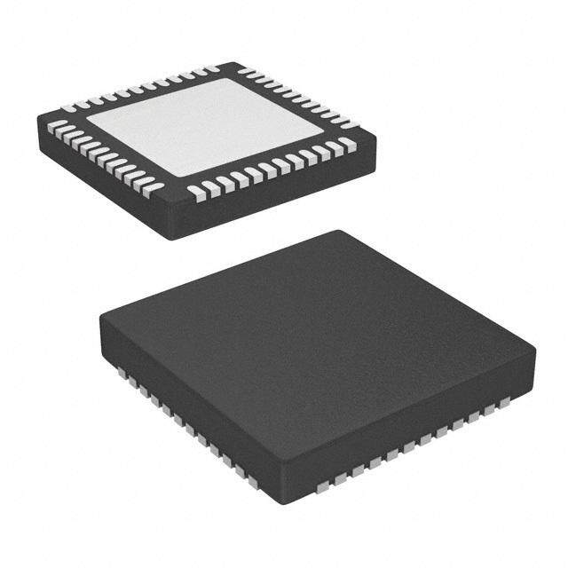
| 供应商器件封装 | 48-TQFN (7x7) |
| 包装 | 管件 |
| 商标 | Maxim Integrated |
| 安装类型 | 表面贴装 |
| 封装 | Tube |
| 封装/外壳 | 48-WFQFN 裸露焊盘 |
| 工作温度 | -40°C ~ 85°C |
| 工厂包装数量 | 43 |
| 应用 | TFT-LCD 面板:伽玛缓冲器,VCOM 驱动器 |
| 标准包装 | 1 |
| 电压-电源 | 8 V ~ 16.5 V |
| 电流-电源 | 8.5mA |
| 系列 | MAX17126 |
| 零件号别名 | MAX17126 |


PDF Datasheet 数据手册内容提取
EVALUATION KIT AVAILABLE MAX17126B Multi-Output Power Supplies with VCOM Amplifier and High-Voltage Gamma Reference for LCD TVs General Description Features The MAX17126B generates all the supply rails for thin- S 8.0V to 16.5V IN Supply Voltage Range film transistor liquid-crystal display (TFT LCD) TV panels S Selectable Frequency (500kHz/750kHz) operating from a regulated 12V input. They include a S Current-Mode Step-Up Regulator step-down and a step-up regulator, a positive and a Fast Load-Transient Response negative charge pump, an operational amplifier, a high- High-Accuracy Output Voltage (1.0%) accuracy high-voltage gamma reference, and a high- Built-In 20V, 3.5A, 100mI MOSFET voltage switch control block. The device can operate High Efficiency from input voltages from 8V to 16.5V and is optimized Adjustable Soft-Start for an LCD TV panel running directly from 12V supplies. Adjustable Current Limit The step-up and step-down switching regulators feature Low Duty-Cycle Operation (13.2VIN - 13.5V AVDD) internal power MOSFETs and high-frequency opera- S Current-Mode Step-Down Regulator tion allowing the use of small inductors and capacitors, Fast Load-Transient Response resulting in a compact solution. The step-up regulator Built-In 20V, 3.2A, 100mI MOSFET provides TFT source driver supply voltage, while the High Efficiency step-down regulator provides the system with logic sup- 3ms Internal Soft-Start ply voltage. Both regulators use fixed-frequency current- mode control architectures, providing fast load-transient S Adjustable Positive Charge-Pump Regulator response and easy compensation. A current-limit func- S Adjustable Negative Charge-Pump Regulator tion for internal switches and output-fault shutdown S Integrated High-Voltage Switch with Adjustable protects the step-up and step-down power supplies Turn-On Delay against fault conditions. The device provides soft-start functions to limit inrush current during startup. In addi- S High-Speed Operational Amplifier tion, the device integrates a control block that can drive ±200mA Short-Circuit Current an external p-channel MOSFET to sequence power to 45V/µs Slew Rate source drivers. S High-Accuracy Reference for Gamma Buffer The positive and negative charge-pump regulators pro- ±1% Feedback Voltage vide TFT gate-driver supply voltages. Both output volt- Up to 30mA Load Current ages can be adjusted with external resistive voltage- Low-Dropout Voltage 0.5V at 60mA dividers. A logic-controlled, high-voltage switch block S External p-Channel Gate Control for AVDD allows the manipulation of the positive gate-driver supply. Sequencing The device includes one high-current operational ampli- S XAO Comparator fier designed to drive the LCD backplane (VCOM). The S Input Undervoltage Lockout and Thermal- amplifier features high output current (Q200mA), fast Overload Protection slew rate (45V/Fs), wide bandwidth (20MHz), and rail-to- rail outputs. S 48-Pin, 7mm x 7mm, TQFN Package Also featured in the device is a high-accuracy, high- Ordering Information voltage adjustable reference for gamma correction. The device is available in a small (7mm x 7mm), ultra-thin PART TEMP RANGE PIN-PACKAGE (0.8mm), 48-pin TQFN package and operates over the MAX17126BETM+ -40NC to +85NC 48 TQFN-EP* -40NC to +85NC temperature range. +Denotes a lead(Pb)-free/RoHS-compliant package. *EP = Exposed pad. Applications LCD TV Panels Visit www.maximintegrated.com/products/patents for product patent marking information. For pricing, delivery, and ordering information, please contact Maxim Direct at 1-888-629-4642, or visit Maxim’s website at www.maximintegrated.com. 19-6050; Rev 0; 9/11
MAX17126B Multi-Output Power Supplies with VCOM Amplifier and High-Voltage Gamma Reference for LCD TVs ABSOLUTE MAXIMUM RATINGS INVL, IN2, VOP, EN, FSEL to GND .......................-0.3V to +24V VREF_I to GND ......................................................-0.3V to +24V PGND, OGND, CPGND to GND ..........................-0.3V to +0.3V VREF_O to GND .......................................-0.3V, (VREF_I + 0.3)V DLY1, GVOFF, THR, VL to GND ..........................-0.3V to +7.5V REF Short Circuit to GND ..........................................Continuous REF, FBP, FBN, FB1, FB2, COMP, SS, CLIM, RMS LX1 Current (total for both pins) ..................................3.2A XAO, VDET, VREF_FB, OUT to GND .............-0.3V, (VL+ 0.3) RMS PGND CURRENT (total for both pins) .........................3.2A GD, GD_I to GND ..................................................-0.3V to +24V RMS IN2 Current (total for both pins) ..................................3.2A LX1 to PGND .........................................................-0.3V to +24V RMS LX2 Current (total for both pins) ..................................3.2A OPP, OPN, OPO to OGND .......................-0.3V to (VOP + 0.3V) RMS DRVN, DRVP Current ..................................................0.8A DRVP to CPGND ....................................-0.3V to (SUPP + 0.3V) RMS VL Current ..................................................................50mA DRVN to CPGND ....................................-0.3V to (SUPN + 0.3V) Continuous Power Dissipation (TA = +70NC) LX2 to PGND ................................................-0.7 to (IN2 + 0.3V) TQFN (derated 38.5mW/NC above +70NC) ............3076.9mW SUPN to GND .............................................-0.3V to (IN2 + 0.3V) Junction Temperature .....................................................+160NC SUPP to GND ..........................................-0.3V to (GD_I + 0.3V) Storage Temperature Range ............................-65NC to +165NC BST to VL ...............................................................-0.3V to +30V Lead Temperature (soldering, 10s) ................................+300NC VGH to GND ..........................................................-0.3V to +40V Soldering Temperature (reflow) ......................................+260NC VGHM, DRN to GND .....................................-0.3V, VGH + 0.3V VGHM to DRN .......................................................-0.3V to +40V Stresses beyond those listed under “Absolute Maximum Ratings” may cause permanent damage to the device. These are stress ratings only, and functional operation of the device at these or any other conditions beyond those indicated in the operational sections of the specifications is not implied. Exposure to absolute maximum rating conditions for extended periods may affect device reliability. ELECTRICAL CHARACTERISTICS (Circuit of Figure 1, VINVL= VIN2 = 12V, VVOP = VVREF_I = 15V, TA = 0°C to +85°C. Typical values are at TA = +25NC, unless oth- erwise noted.) PARAMETER CONDITIONS MIN TYP MAX UNITS GENERAL INVL, IN2 Input Voltage Range 8 16.5 V Only LX2 switching (VFB1 = VFBP = 1.5V, VFBN = 0V) INVL + IN2 Quiescent Current 10 20 mA EN = VL, FSEL = high LX2 not switching (VFB1 = VFB2 = VFBP = 1.5V, INVL + IN2 Standby Current 24 5 mA VFBN = 0V), EN = VL, FSEL = high FSEL = INVL or high impedance 630 750 870 SMPS Operating Frequency kHz FSEL = GND 420 500 580 INVL Undervoltage-Lockout INVL rising, 150mV typical hysteresis 6.0 7.0 8.0 V Threshold VL REGULATOR IVL = 25mA, VFB1 = VFB2 = VFBP = 1.1V, VFBN = 0.4V VL Output Voltage 4.85 5 5.15 V (all regulators switching) VL Undervoltage-Lockout VL rising, 50mV typical hysteresis 3.5 3.9 4.3 V Threshold REFERENCE REF Output Voltage No external load 1.2375 1.250 1.2625 V REF Load Regulation 0V < ILOAD < 50FA 5 mV REF Sink Current In regulation 10 FA REF Undervoltage-Lockout Rising edge, 250mV typical hysteresis 1.0 1.2 V Threshold 2 Maxim Integrated
MAX17126B Multi-Output Power Supplies with VCOM Amplifier and High-Voltage Gamma Reference for LCD TVs ELECTRICAL CHARACTERISTICS (continued) (Circuit of Figure 1, VINVL= VIN2 = 12V, VVOP = VVREF_I = 15V, TA = 0°C to +85°C. Typical values are at TA = +25NC, unless oth- erwise noted.) PARAMETER CONDITIONS MIN TYP MAX UNITS STEP-DOWN REGULATOR FB2 = GND, no load 0°C < TA = +85°C 3.25 3.3 3.35 OUT Voltage in Fixed Mode V (Note 1) TA = +25°C 3.267 3.333 FB2 Voltage in Adjustable VOUT = 2.5V, no load 0°C < TA = +85°C 1.23 1.25 1.27 V Mode (Note 1) TA = +25°C 1.2375 1.2625 FB2 Adjustable Mode Threshold Dual Mode™ comparator 0.10 0.15 0.20 V Voltage Output Voltage Adjust Range 1.5 5 V FB2 Fault-Trip Level Falling edge 0.96 1.0 1.04 V FB2 Input Leakage Current VFB2 = 1.25V 50 125 200 nA DC Load Regulation 0V < ILOAD < 2A 0.5 % DC Line Regulation No load, 10.8V < VIN2 < 13.2V 0.1 %/V LX2-to-IN2 nMOS Switch 100 200 mI On-Resistance LX2-to-GND2 nMOS Switch 6 10 23 I On-Resistance BST-to-VL pMOS Switch 40 30 110 I On-Resistance Low-Frequency Operation LX2 only 0.8 V OUT Threshold Low-Frequency Operation FSEL = INVL 125 kHz Switching Frequency FSEL = GND 83 LX2 Positive Current Limit MAX17126 2.50 3.20 3.90 A Soft-Start Ramp Time Zero to full limit 3 ms Maximum Duty Factor 70 78 85 % Minimum Duty Factor 10 % Char/Design Limit Only STEP-UP REGULATOR Output Voltage Range VIN 20 V Oscillator Maximum Duty Cycle 70 78 85 % FB1 Regulation Voltage FB1 = COMP, CCOMP = 1nF 1.2375 1.25 1.2625 V FB1 Fault Trip Level Falling edge 0.96 1.0 1.04 V FB1 Load Regulation 0V < ILOAD < full 0.5 % FB1 Line Regulation 10.8V < VIN < 13.2V 0.08 %/V FB1 Input Bias Current VFB1 = 1.25V 30 125 200 nA FB1 Transconductance DI = Q2.5FA at COMP, FB1 = COMP 150 320 560 FS FB1 Voltage Gain FB1 to COMP 1400 V/V LX1 Leakage Current VFB1 = 1.5V, VLX1 = 20V 10 40 FA Dual Mode is a trademark of Maxim Integrated Products, Inc. Maxim Integrated 3
MAX17126B Multi-Output Power Supplies with VCOM Amplifier and High-Voltage Gamma Reference for LCD TVs ELECTRICAL CHARACTERISTICS (continued) (Circuit of Figure 1, VINVL= VIN2 = 12V, VVOP = VVREF_I = 15V, TA = 0°C to +85°C. Typical values are at TA = +25NC, unless oth- erwise noted.) PARAMETER CONDITIONS MIN TYP MAX UNITS VFB1 = 1.1V, RCLIM = unconnected 3.0 3.5 4.2 3.5 - LX1 Current Limit A VFB1 = 1.1V, with RCLIM at CLIM pin -20% (68k/ +20% RCLIM) CLIM Voltage RCLIM = 60.5kI 0.56 0.625 0.69 V Current-Sense Transresistance 0.19 0.21 0.25 V/A LX1 On-Resistance 100 185 mI Soft-Start Period CSS < 200pF 16 ms SS Charge Current VSS = 1.2V 4 5 6 FA POSITIVE CHARGE-PUMP REGULATORS GD_I Input Supply Range 8.0 20 V GD_I Input Supply Current VFBP = 1.5V (not switching) 0.15 0.3 mA GD_I Overvoltage Threshold GD_I rising, 250mV typical hysteresis (Note 2) 20.1 21 22 V FBP Regulation Voltage 1.2375 1.25 1.2625 V FBP Line Regulation Error VSUP = 11V to 16V, not in dropout 0.2 %/V FBP Input Bias Current VFBP = 1.5V, TA = +25°C -50 +50 nA DRVP p-Channel MOSFET 1.5 3 I On-Resistance DRVP n-Channel MOSFET 1 2 I On-Resistance FBP Fault Trip Level Falling edge 0.96 1.0 1.04 V 7-bit voltage ramp with filtering to prevent high peak Positive Charge-Pump 4 ms currents 500kHz frequency Soft-Start Period 750kHz frequency 3 ms NEGATIVE CHARGE-PUMP REGULATORS FBN Regulation Voltage VREF - VFBN 0.99 1.00 1.01 V FBN Input Bias Current VFBN = 0mV, TA = +25°C -50 +50 nA FBN Line Regulation Error VIN2 = 11V to 16V, not in dropout 0.2 %/V DRVN PCH On-Resistance 1.5 3 I DRVN NCH On-Resistance 1 2 I FBN Fault Trip Level Rising edge 720 800 880 mV 7-bit voltage ramp with filtering to prevent high peak Negative Charge-Pump Soft- 3 currents 500kHz frequency ms Start Period 750kHz frequency 2 AVDD SWITCH GATE CONTROL GD to GD_I Pullup Resistance EN = GND 25 50 I GD Output Sink Current EN = VL 5 10 15 FA GD Done Threshold EN = VL, VGD_I - VGD 5 6 7 V OPERATIONAL AMPLIFIERS VOP Supply Range 8 20 V 4 Maxim Integrated
MAX17126B Multi-Output Power Supplies with VCOM Amplifier and High-Voltage Gamma Reference for LCD TVs ELECTRICAL CHARACTERISTICS (continued) (Circuit of Figure 1, VINVL= VIN2 = 12V, VVOP = VVREF_I = 15V, TA = 0°C to +85°C. Typical values are at TA = +25NC, unless oth- erwise noted.) PARAMETER CONDITIONS MIN TYP MAX UNITS VOP Overvoltage Fault VVOP = rising, hysteresis = 200mV (Note 2) 20.1 21 22 V Threshold VOP Supply Current Buffer configuration, VOPP = VOPN = VOP/2, no load -10 -2 +6 mA Input Offset Voltage 2V < (VOPP, VOPN ) < (VVOP - 2V) 3 14 mV Input Bias Current 2V < (VOPP, VOPN ) < (VVOP - 2V) -1 +1 FA Input Common-Mode 0 VOP V Voltage Range Input Common-Mode 2V < (VOPP, VOPN ) < (VVOP - 2V) 80 dB Rejection Ratio VOP - VOP - Output Voltage Swing High IOPO = 25mA mV 320 150 Output Voltage Swing Low IOPO = -25mA 150 300 mV Large-Signal Voltage Gain 2V < (VOPP, VOPN ) < (VOP - 2V) 80 dB Slew Rate 2V < (VOPP, VOPN ) < (VOP - 2V) 45 V/Fs -3dB Bandwidth 2V < (VOPP, VOPN ) < (VOP - 2V) 20 MHz Short to VVOP/2, sourcing 200 Short-Circuit Current mA Short to VVOP/2, sinking 200 HIGH-VOLTAGE SWITCH ARRAY VGH Supply Range 35 V VGH Supply Current 150 300 FA VGHM-to-VGH Switch VDLY1 = 2V, GVOFF = VL 5 10 I On-Resistance VGHM-to-VGH Switch VVGH - VVGHM > 5V 150 390 mA Saturation Current VGHM-to-DRN Switch VDLY1 = 2V, GVOFF = GND 20 50 I On-Resistance VGHM-to-DRN Switch VVGHM - VDRN > 5V 75 200 mA Saturation Current VGHM-to-GND Switch DLY1 = GND 1.0 2.5 4.0 kI On-Resistance GVOFF Input Low Voltage 0.6 V GVOFF Input High Voltage 1.6 V GVOFF Input Current VGVOFF = 0V or VL, TA = +25°C -1 +1 FA 1kI from DRN to CPGND, VGVOFF = 0V to VL step, no GVOFF-to-VGHM Rising load on VGHM, measured from GVOFF = 2V to VGHM 100 ns Propagation Delay = 20% 1kI from DRN to CPGND, VGVOFF = VL to 0V step, no GVOFF-to-VGHM Falling load on VGHM, DRN falling, no load on DRN and VGHM, 200 ns Propagation Delay measured from VGVOFF = 0.6V to VGHM = 80% THR-to-VGHM Voltage Gain 9.4 10 10.6 V/V Maxim Integrated 5
MAX17126B Multi-Output Power Supplies with VCOM Amplifier and High-Voltage Gamma Reference for LCD TVs ELECTRICAL CHARACTERISTICS (continued) (Circuit of Figure 1, VINVL= VIN2 = 12V, VVOP = VVREF_I = 15V, TA = 0°C to +85°C. Typical values are at TA = +25NC, unless oth- erwise noted.) PARAMETER CONDITIONS MIN TYP MAX UNITS SEQUENCE CONTROL EN Pulldown Resistance 1 MI VDLY1 = 1V; when DLY1 cap is not used, there is no DLY1 Charge Current 6 8 10 FA delay EN, DLY1 Turn-On Threshold 1.19 1.25 1.31 V DLY1 Discharge Switch EN = GND or fault tripped 10 I On-Resistance FBN Discharge Switch (EN = GND and INVL < UVLO) or fault tripped 3 kI On-Resistance GAMMA REFERENCE VREF_I Input Voltage Range 10 18.0 V VREF_I Input Bias Current No load 125 250 FA VREF_O Dropout Voltage IVREF_O = 60mA 0.25 0.5 V VVREF_I = 13.5V, 1mA P IVREF_O P 30mA, VVREF_O = 9.5V 1.243 1.250 1.256 V VREF_FB Regulation Voltage VVREF_I from 10V to 18V, IVREF_O = 20mA, VVREF_O = 9.5V P 0.9 mV/V VREF_O Maximum Output 60 mA Current XAO FUNCTION VDET Threshold VDET rising 1.225 1.25 1.275 V VDET Hysteresis 50 mV VDET Input Bias Current 50 175 300 nA XAO Output Voltage VDET = AGND, IPGOOD = 1mA 0.4 V FAULT DETECTION Duration-to-Trigger Fault For UVP only 50 ms 0.36 x 0.4 x 0.44 x Step-Up Short-Circuit Protection FB1 falling edge V VREF VREF VREF 0.18 x 0.2 x 0.22 x Adjustable mode FB2 falling Step-Down Short-Circuit VREF VREF VREF V Protection Fixed mode OUT falling, internal feedback divider 0.18 x 0.2 x 0.22 x voltage VREF VREF VREF Positive Charge-Pump 0.36 x 0.4 x 0.44 x FBP falling edge V Short-Circuit Protection VREF VREF VREF Negative Charge-Pump VREF - VFBN 0.4 0.45 0.5 V Short-Circuit Protection Thermal-Shutdown Threshold Latch protection +160 NC SWITCHING FREQUENCY SELECTION FSEL Input Low Voltage 500kHz 0.6 V FSEL Input High Voltage 750kHz 1.6 V FSEL Pullup Resistance 1 MI 6 Maxim Integrated
MAX17126B Multi-Output Power Supplies with VCOM Amplifier and High-Voltage Gamma Reference for LCD TVs ELECTRICAL CHARACTERISTICS (VINVL = VIN2 = 12V, VVOP = VVREF_I = 15V, TA = -40NC to +85NC.) (Note 3) PARAMETER CONDITIONS MIN TYP MAX UNITS GENERAL INVL, IN2 Input-Voltage Range 8 16.5 V FSEL = INVL or high impedance 630 870 SMPS Operating Frequency kHz FSEL = GND 420 580 INVL Undervoltage-Lockout INVL rising, 150mV typical hysteresis 6.0 8.0 V Threshold VL REGULATOR IVL = 25mA, VFB1 = VFB2 = VFB = 1.1V, VFBN = 0.4V VL Output Voltage 4.85 5.15 V (all regulators switching) VL Undervoltage-Lockout VL rising, 50mV typical hysteresis 3.5 4.3 V Threshold REFERENCE REF Output Voltage No external load 1.235 1.265 V REF Undervoltage-Lockout Rising edge, 25mV typical hysteresis 1.2 V Threshold STEP-DOWN REGULATOR OUT Voltage in Fixed Mode FB2 = GND, no load (Note 1) 3.267 3.333 V FB2 Voltage in Adjustable Mode VOUT = 2.5V, no load (Note 1) 1.2375 1.2625 V FB2 Adjustable Mode Dual-mode comparator 0.10 0.20 V Threshold Voltage Output Voltage Adjust Range 1.5 5 V FB2 Fault Trip Level Falling edge 0.96 1.04 V LX2-to-IN2 nMOS Switch 200 mI On-Resistance LX2-to-GND2 nMOS Switch 6 23 I On-Resistance BST-to-VL pMOS Switch 40 110 I On-Resistance LX2 Positive Current Limit MAX17126 2.50 3.90 A Maximum Duty Factor 70 85 % Maxim Integrated 7
MAX17126B Multi-Output Power Supplies with VCOM Amplifier and High-Voltage Gamma Reference for LCD TVs ELECTRICAL CHARACTERISTICS (continued) (VINVL = VIN2 = 12V, VVOP = VVREF_I = 15V, TA = -40NC to +85NC.) (Note 3) PARAMETER CONDITIONS MIN TYP MAX UNITS STEP-UP REGULATOR Output-Voltage Range VIN 20 V Oscillator Maximum Duty Cycle 70 85 % FB1 Regulation Voltage FB1 = COMP, CCOMP = 1nF 1.2375 1.2625 V FB1 Fault Trip Level Falling edge 0.96 1.04 V FB1 Transconductance DI = Q2.5FA at COMP, FB1 = COMP 150 560 FS LX1 Input Bias Current VFB1 = 1.5V, VLX1 = 20V 40 FA VFB1 = 1.1V, RCLIM = unconnected 3.0 4.2 LX1 Current Limit VFB1 = 1.1V , with RCLIM at CLIM pin, A -20% +20% limit = 3.5A - (68kW/RCLIM) CLIM Voltage RCLIM = 60.5kI 0.56 0.69 V Current-Sense Transresistance 0.19 0.25 V/A LX1 On-Resistance 185 mI SS Charge Current VSS = 1.2V 4 6 FA POSITIVE CHARGE-PUMP REGULATORS GD_I Input Supply Range 8.0 20 V GD_I Input Supply Current VFBP = 1.5V (not switching) 0.2 mA GD_I Overvoltage Threshold GD_I rising, 250mV typical hysteresis (Note 2) 20.1 22 V FBP Regulation Voltage 1.243 1.256 V FBP Line Regulation Error VSUP = 11V to 16V, not in dropout 0.2 %/V DRVP p-Channel MOSFET 3 I On-Resistance DRVP n-Channel MOSFET 1 I On-Resistance FBP Fault Trip Level Falling edge 0.96 1.04 V NEGATIVE CHARGE-PUMP REGULATORS FBN Regulation Voltage VREF - VFBN 0.99 1.01 V FBN Line Regulation Error VIN2 = 11V to 16V, not in dropout 0.2 %/V DRVN PCH On-Resistance 3 I DRVN NCH On-Resistance 1 I FBN Fault Trip Level Rising edge 720 880 mV AVDD SWITCH GATE CONTROL GD Output Sink Current EN = VL 5 15 FA GD Done Threshold EN = VL, VGD_I - VGD 5 7 V 8 Maxim Integrated
MAX17126B Multi-Output Power Supplies with VCOM Amplifier and High-Voltage Gamma Reference for LCD TVs ELECTRICAL CHARACTERISTICS (continued) (VINVL = VIN2 = 12V, VVOP = VVREF_I = 15V, TA = -40NC to +85NC.) (Note 3) PARAMETER CONDITIONS MIN TYP MAX UNITS OPERATIONAL AMPLIFIERS VOP Supply Range 8 20 V VOP Overvoltage Fault Threshold VOP = rising, hysteresis = 200mV (Note 2) 20.1 22 V VOP Supply Current Buffer configuration, VOPP = VOPN = VOP/2, no load 4 mA Input Offset Voltage 2V < (VOPP, VOPN ) < (VOP - 2V) -12 +8 mV Input Common-Mode 0 OVIN V Voltage Range VOP - Output Voltage Swing High IOPO = 25mA mV 320 Output Voltage Swing Low IOPO = -25mA 300 mV Short to VOPO/2, sourcing 200 Short-Circuit Current mA Short to VOPO/2, sinking 200 HIGH-VOLTAGE SWITCH ARRAY VGH Supply Range 35 V VGH Supply Current 300 FA VGHM-to-VGH Switch VDLY1 = 2V, GVOFF = VL 10 I On-Resistance VGHM-to-VGH Switch VVGH - VVGHM > 5V 150 mA Saturation Current VGHM-to-DRN Switch VDLY1 = 2V, GVOFF = GND 50 I On-Resistance VGHM-to-DRN Switch VVGHM - VDRN > 5V 75 mA Saturation Current VGHM-to-GND Switch DLY1 = GND 1.0 4.0 kI On-Resistance GVOFF Input Low Voltage 0.6 V GVOFF Input High Voltage 1.6 V THR-to-VGHM Voltage Gain 9.4 10.6 V/V SEQUENCE CONTROL EN Input Low Voltage 0.6 V EN Input High Voltage 1.6 V VDLY1 = 1V; when DLY1 cap is not used, DLY1 Charge Current 6 10 FA there is no delay DLY1 Turn-On Threshold 1.19 1.31 V Maxim Integrated 9
MAX17126B Multi-Output Power Supplies with VCOM Amplifier and High-Voltage Gamma Reference for LCD TVs ELECTRICAL CHARACTERISTICS (continued) (VINVL = VIN2 = 12V, VVOP = VVREF_I = 15V, TA = -40NC to +85NC.) (Note 3) PARAMETER CONDITIONS MIN TYP MAX UNITS GAMMA REFERENCE VREF_I Input Voltage Range 10 18.0 V VREF_I Undervoltage Lockout VREF_I rising 5.2 V VREF_I Input Bias Current No load 250 FA VREF_O Dropout Voltage IVREF_O = 60mA 0.5 V VREF_I = 13.5V, 1mA ≤ IVREF_O ≤ 30mA 1.2375 1.2625 V VREF_FB Regulation Voltage VREF_I from 10V to 18V, IVREF_O = 20mA P 0.9 mV/V VREF_O Maximum 60 mA Output Current XAO FUNCTION VDET Threshold VDET rising 1.225 1.275 V XAO Output Voltage VDET = AGND, IPGOOD = 1mA 0.4 V FAULT DETECTION Step-Up Short-Circuit 0.36 x 0.44 x FB1 falling edge V Protection VREF VREF 0.18 x 0.22 x Adjustable mode FB2 falling V Step-Down Short-Circuit VREF VREF Protection Fixed mode OUT falling, internal feedback divider 0.18 x 0.22 x V voltage VREF VREF Positive Charge-Pump 0.36 x 0.44 x FBP falling edge V Short-Circuit Protection VREF VREF Negative Charge-Pump VREF - VFBN 0.4 0.5 V Short-Circuit Protection SWITCHING FREQUENCY SELECTION FSEL Input Low Voltage 500kHz 0.6 V FSEL Input High Voltage 750kHz 1.6 V Note 1: When the step-down inductor is in continuous conduction (EN = VL or heavy load), the output voltage has a DC regulation level lower than the error comparator threshold by 50% of the output voltage ripple. In discontinuous conduction (EN = GND with light load), the output voltage has a DC regulation level higher than the error comparator threshold by 50% of the output voltage ripple. Note 2: Disables boost switching if either GD_I or VOP exceeds the threshold. Switching resumes when no threshold is exceeded. Note 3: Specifications to TA = -40NC are guaranteed by design, not production tested. 10 Maxim Integrated
MAX17126B Multi-Output Power Supplies with VCOM Amplifier and High-Voltage Gamma Reference for LCD TVs Typical Operating Characteristics (TA = +25°C, unless otherwise noted.) STEP-DOWN REGULATOR EFFICIENCY STEP-DOWN REGULATOR OUTPUT vs. LOAD CURRENT VOLTAGE vs. LOAD CURRENT 8805 750kHz MAX17126B toc01 3.350 750kHz MAX17126B toc02 75 V) %) E (3.325 EFFICIENCY ( 6750 500kHz UTPUT VOLTAG3.300 60 O 500kHz 55 50 3.275 0.10 1.00 10.00 0 0.42 0.80 1.20 1.60 2.00 2.40 LOAD CURRENT (A) LOAD CURRENT (A) STEP-DOWN REGULATOR LOAD STEP-DOWN REGULATOR HEAVY-LOAD TRANSIENT RESPONSE (0.3A TO 1.8A) SOFT-START (1A) MAX17126B toc03 MAX17126B toc04 VIN 5V/div VOUT 0V (AC-COUPLED) VOUT 200mV/div 0V 1V/div 0V IL2 IL2 1A/div 0A 1A/div 0A ILOAD LX2 0A 1A/div 0A 10V/div 20Fs/div 4ms/div L = 4.7FH STEP-UP REGULATOR EFFICIENCY STEP-UP REGULATOR OUTPUT vs. LOAD CURRENT VOLTAGE vs. LOAD CURRENT 1990050 MAX17126B toc05 1166..444405 MAX17126B toc06 CY (%) 8805 500kHz LTAGE (V)1166..443305 EN 75 VO 750kHz EFFICI 6750 750kHz OUTPUT 1166..442205 500kHz 60 16.415 55 50 16.410 0.01 0.10 1.00 10.00 0 0.5 1.0 1.5 2.0 2.5 LOAD CURRENT (A) LOAD CURRENT (A) Maxim Integrated 11
MAX17126B Multi-Output Power Supplies with VCOM Amplifier and High-Voltage Gamma Reference for LCD TVs Typical Operating Characteristics (continued) (TA = +25°C, unless otherwise noted.) STEP-UP REGULATOR LOAD TRANSIENT STEP-UP REGULATOR PULSED LOAD RESPONSE (0.1A TO 1.1A) TRANSIENT RESPONSE (0.1A TO 1.9mA) MAX17126B toc07 MAX17126B toc08 ILOAD 0V ILOAD 0V 1A/div 1A/div VAVDD VAVDD 0A (AC-COUPLED) 0A (AC-COUPLED) 200mV/div 200mV/div IL1 IL1 0A 1A/div 0A 1A/div 20Fs/div 10Fs/div L = 10FH L = 10FH STEP-UP REGULATOR HEAVY LOAD SWITCHING FREQUENCY SOFT-START (0.5A) vs. INPUT VOLTAGE MAX17126B toc09 498 0V E5NV/div Hz) 449967 MAX17126B toc10 VAVDD Y (k 495 5V/div NC 494 0V VGD QUE 493 5V/div RE G F 492 N HI 491 0V TC WI 490 IL1 S 489 1A/div 0A 488 1ms/div 8 10 12 14 16 VIN (V) REFERENCE VOLTAGE LOAD GAMMA REFERENCE LINE REGULATION GAMMA REFERENCE LOAD REGULATION (LOAD = 20mA) REGULATION (VREF = 16V) REFERENCE VOLTAGE (V)1111....2222444478895050 NO SWITCHINSGWITCHING MAX17126B toc11 MMA REFERENCE VOLTAGE (V)1111144555.....9900149494 MAX17126B toc12 MMA REFERENCE VOLTAGE (V)111111444555......789012 MAX17126B toc13 1.2470 GA14.89 GA14.6 1.2465 14.84 14.5 0 50 100 150 200 15.0 15.5 16.0 16.5 17.0 17.5 18.0 0 50 100 150 200 250 LOAD CURRENT (FA) VOP VOLTAGE (V) LOAD CURRENT (mA) 12 Maxim Integrated
MAX17126B Multi-Output Power Supplies with VCOM Amplifier and High-Voltage Gamma Reference for LCD TVs Typical Operating Characteristics (continued) (TA = +25°C, unless otherwise noted.) POSITIVE CHARGE-PUMP REGULATOR POSITIVE CHARGE-PUMP REGULATOR NORMALIZED LINE REGULATION NORMALIZED LOAD REGULATION 2 0.5 -20 IGON = 0A MAX17126B toc14 R (%) 0 MAX17126B toc15 V ERROR (%)GON --64 IGON = 25mA UT CURRENT ERRO --10..05 -8 TP U O -1.5 -10 -12 -2.0 10 11 12 13 14 15 16 17 18 0 50 100 150 SUPP VOLTAGE (V) LOAD CURRENT (mA) NEGATIVE CHARGE-PUMP REGULATOR POSITIVE CHARGE-PUMP REGULATOR NORMALIZED LINE REGULATION LOAD-TRANSIENT RESPONSE MAX17126B toc16 0.001 IGON = 25mA MAX17126B toc17 0V V(AGCO-CNOUPLED) OR (%)-0.01 200mV/div RR IGON = 0mA E OFF-0.02 60mA VG ILOAD -0.03 20mA/div 0A 10mA -0.04 8 9 10 11 12 13 14 15 16 40Fs/div SUPN VOLTAGE (V) NEGATIVE CHARGE-PUMP REGULATOR NEGATIVE CHARGE-PUMP REGULATOR NORMALIZED LOAD REGULATION LOAD TRANSIENT RESPONSE 0.2 MAX17126B toc19 R (%) -0.02 MAX17126B toc18 RO VGOFF R 0V E (AC-COUPLED) GE -0.4 200mV/div A T OL -0.6 T V 60mA U UTP -0.8 ILOAD O 20mA/div -1.0 0A 10mA -1.2 0 50 100 150 200 250 300 20Fs/div LOAD CURRENT (mA) Maxim Integrated 13
MAX17126B Multi-Output Power Supplies with VCOM Amplifier and High-Voltage Gamma Reference for LCD TVs Typical Operating Characteristics (continued) (TA = +25°C, unless otherwise noted.) POWER-UP SEQUENCE OF ALL OP AMP SUPPLY CURRENT SUPPLY OUTPUTS vs. SUPPLY VOLTAGE MAX17126B toc20 2.65 00VV VVIONUT A)m2.60 MAX17126B toc21 0V T (2.55 VGOFF EN 0V VAVDD URR2.50 VGON Y C PL2.45 0V UP S 0V VCOM OP 2.40 0V VDLY1 V 0V VGHM 2.35 0V 2.30 10ms/div 8 9 10 11 12 13 14 15 16 17 18 19 20 VIN = 10V/div VGON = 20V/div VOUT = 5V/div VCOM = 10V/div VOP VOLTAGE (V) VGOFF = 10V/div VDLY1 = 5V/div VAVDD =10V/div VGHM = 50V/div OPERATIONAL AMPLIFIER RAIL-TO-RAIL OPERATIONAL AMPLIFIER LOAD INPUT/OUTPUT WAVEFORMS TRANSIENT RESPONSE MAX17126B toc22 MAX17126B toc23 VOPP 5V/div VCOM 0V (AC-COUPLED) 500mV/div 0V VCOM 5V/div IVCOM 0A 100mA/div 0V 4Fs/div 1Fs/div OPERATIONAL AMPLIFIER OPERATIONAL AMPLIFIER LARGE-SIGNAL STEP RESPONSE SMALL-SIGNAL STEP RESPONSE MAX17126B toc24 MAX17126B toc25 VOPP 0V VOPP 0V (AC-COUPLED) 5V/div 200mV/div VCOM 0V (AC-COUPLED) VCOM 200mV/div 0V 5V/div 1Fs/div 100ns/div 14 Maxim Integrated
MAX17126B Multi-Output Power Supplies with VCOM Amplifier and High-Voltage Gamma Reference for LCD TVs Typical Operating Characteristics (continued) (TA = +25°C, unless otherwise noted.) HIGH-VOLTAGE SWITCH CONTROL VIN SUPPLY CURRENT vs. VIN VOLTAGE FUNCTION (VGHM WITH 470pF LOAD) 7 MAX17126B toc27 6 ALL OUTPUT SWITCHING MAX17126B toc26 5VVG/VdOiFvF A) 5 0V m BUCK OUTPUT SWITCHING NT ( 4 VGHM RRE NO OUTPUT SWITCHING 10V/div CU 3 L V N I 2 0V 1 0 8 10 12 14 16 4Fs/div INPUT VOLTAGE (V) Pin Configuration TOP VIEW DRVP CPGND SUPP THR COMP FB1 GD GD_I PGND PGND LX1 LX1 36 35 34 33 32 31 30 29 28 27 26 25 DLY1 37 24 SS FBP 38 23 CLIM VGH 39 22 FSEL VGHM 40 21 VL DRN 41 20 INVL SUPN 42 19 VDET MAX17126B DRVN 43 18 GND GND 44 17 IN2 FBN 45 16 IN2 REF 46 15 BST VREF_FB 47 14 LX2 VREF_O 48 13 LX2 1 2 3 4 5 6 7 8 9 10 11 12 VREF_I VOP OGND OPP OPN OPO XAO GVOFF EN FB2 OUT N.C. TQFN Maxim Integrated 15
MAX17126B Multi-Output Power Supplies with VCOM Amplifier and High-Voltage Gamma Reference for LCD TVs Pin Description PIN NAME FUNCTION 1 VREF_I Gamma Reference Input 2 VOP Operational Amplifier Power Supply 3 OGND Operational Amplifier Power Ground 4 OPP Operational Amplifier Noninverting Input 5 OPN Operational Amplifier Inverting Input 6 OPO Operational Amplifier Output 7 XAO Voltage Detector Output High-Voltage Switch-Control Block Timing Control Input. See the High-Voltage Switch Control 8 GVOFF section for details. 9 EN Enable Input. Enable is high, turns on step-up converter and positive charge pump. Step-Down Regulator Feedback Input. Connect FB2 to GND to select the step-down converter’s 3.3V fixed mode. For adjustable mode, connect FB2 to the center of a resistive voltage-divider between the 10 FB2 step-down regulator output (OUT) and GND to set the step-down regulator output voltage. Place the resistive voltage-divider within 5mm of FB2. 11 OUT Step-Down Regulator Output Voltage Sense. Connect OUT to step-down regulator output. 12 N.C. Not Connected Step-Down Regulator Switching Node. LX2 is the source of the internal n-channel MOSFET connected 13, 14 LX2 between IN2 and LX2. Connect the inductor and Schottky catch diode to both LX2 pins and minimize the trace area for lowest EMI. Step-Down Regulator Bootstrap Capacitor Connection. Power supply for high-side gate driver. Connect 15 BST a 0.1FF ceramic capacitor from BST to LX2. Step-Down Regulator Power Input. Drain of the internal n-channel MOSFET connected between IN2 16, 17 IN2 and LX2. 18, 44 GND Analog Ground Voltage-Detector Input. Connects VDET to the center of a resistor voltage-divider between input voltage 19 VDET and GND to set the trigger point of XAO. Internal 5V Linear Regulator and the Startup Circuitry Power Supply. Bypass VINVL to GND with 0.22FF 20 INVL close to the IC. 5V Internal Linear Regulator Output. Bypass VL to GND with 1FF minimum. Provides power for the internal MOSFET driving circuit, the PWM controllers, charge-pump regulators, logic, and reference 21 VL and other analog circuitry. Provides 25mA load current when all switching regulators are enabled. VL is active whenever input voltage is high enough. Frequency Select Pin. Connect FSEL to VL or INVL or disconnect FSEL pin for 750kHz operation. 22 FSEL Connect to GND for 500kHz operation. Boost Current-Limit Setting Input. Connects a resistor from CLIM to GND to set current limit for boost 23 CLIM converter. Soft-Start Input. Connects a capacitor from SS to GND to set the soft-start time for the step-up converter. A 5FA current source starts to charge CSS when GD is done. See the Step-Up Regulator External pMOS 24 SS Pass Switch section for description. SS is internally pulled to GND through 1kI resistance when EN is low OR when VL is below its UVLO threshold. Step-Up Regulator Power-MOSFET n-Channel Drain and Switching Node. Connects the inductor and 25, 26 LX1 Schottky catch diode to both LX1 pins and minimizes the trace area for lowest EMI. 27, 28 PGND Step-Up Regulator Power Ground Step-Up Regulator External pMOS Pass Switch Source Input. Connects to the cathode of the step-up 29 GD_I regulator Schottky catch diode. 16 Maxim Integrated
MAX17126B Multi-Output Power Supplies with VCOM Amplifier and High-Voltage Gamma Reference for LCD TVs Pin Description (continued) PIN NAME FUNCTION Step-Up Regulator External pMOS Pass Switch Gate Input. A 10FA P 20% current source pulls down on 30 GD the gate of the external pFET when EN is high. Boost Regulator Feedback Input. Connects FB1 to the center of a resistive voltage-divider between the 31 FB1 boost regulator output and GND to set the boost regulator output voltage. Place the resistive voltage- divider within 5mm of FB1. Compensation Pin for the Step-Up Regulator Error Amplifier. Connects a series resistor and capacitor 32 COMP from COMP to ground. VGHM Low-Level Regulation Set-Point Input. Connects THR to the center of a resistive voltage-divider 33 THR between AVDD and GND to set the VGHM falling regulation level. The actual level is 10 x VTHR. See the Switch Control section for details. Positive Charge-Pump Drivers Power Supply. Connects to the output of the boost regulator (AVDD) and 34 SUPP bypasses to CPGND with a 0.1FF capacitor. SUPP is internally connected to GD_I. 35 CPGND Charge Pump and Buck Power Ground 36 DRVP Positive Charge-Pump Driver Output. Connects DRVP to the positive charge-pump flying capacitor(s). High-Voltage Switch Array Delay Input. Connects a capacitor from DLY1 to GND to set the delay time between when the positive charge pump finishes its soft-start and the startup of this high-voltage switch 37 DLY1 array. A 10FA current source charges CDLY1. DLY1 is internally pulled to GND through 50I resistance when EN is low or when VL is below its UVLO threshold. Positive Charge-Pump Regulator Feedback Input. Connects FBP to the center of a resistive voltage- 38 FBP divider between the positive charge-pump regulator output and GND to set the positive charge-pump regulator output voltage. Place the resistive voltage-divider within 5mm of FBP. 39 VGH Switch Input. Source of the internal high-voltage p-channel MOSFET between VGH and VGHM. Internal High-Voltage MOSFET Switch Common Terminal. VGHM is the output of the high-voltage switch- 40 VGHM control block. 41 DRN Switch Output. Drain of the internal high-voltage p-channel MOSFET connected to VGHM. Negative Charge-Pump Drivers Power Supply. Bypass to CPGND with a 0.1FF capacitor. SUPN is 42 SUPN internally connected to IN2. 43 DRVN Negative Charge-Pump Driver Output. Connects DRVN to the negative charge-pump flying capacitor(s). Negative Charge-Pump Regulator Feedback Input. Connect FBN to the center of a resistive voltage- 45 FBN divider between the negative output and REF to set the negative charge-pump regulator output voltage. Place the resistive voltage-divider within 5mm of FBN. Reference Output. Connects a 0.22FF capacitor from REF to GND. All power outputs are disabled until 46 REF REF exceeds its UVLO threshold. Gamma Reference Feedback Input. Connect VREF_FB to the center of a resistive voltage-divider 47 VREF_FB between VREF_O and GND to set the gamma reference output voltage. Place the resistive voltage- divider within 5mm of VREF_FB. 48 VREF_O Gamma Reference Output Exposed Pad. Connects EP to GND, and ties EP to a copper plane or island. Maximizes the area of this — EP copper plane or island to improve thermal performance. Maxim Integrated 17
MAX17126B Multi-Output Power Supplies with VCOM Amplifier and High-Voltage Gamma Reference for LCD TVs VIN 12V C1 L1 10µH 0.1µF D1 BST LX1 IN2 LX1 C2 C4 IN2 PGND PGND FB1 COMP R2 3.3V, 1O.U5AT L2 LX2 FSEL R2C5OkMIP C1nCFOMP C5 D2 LX2 CLIM R1 OUT GD_I Q1 GD VL (OR 3.3V) FB2 MAX17126B 10kI VIN XAO 68.1kRI7 A16VVD,D 1A VIN INVL VDET C3 0.1µF R8 422kI VL VL VOP 1µF OPP 0.1µF 13.3kI REF REF OPN 0.22µF OPO GND OGND 2.2kI 1kI ON/OFF EN DRN 13.3kI DLY1 VCOM 0.1µF THR SS 3Ω UNCONNECTED OR 150nF FROM 2.2kI GVOFF TCON 150µF AVDD VREF_I VGHM VGHM GREF VREF_O VGH R9 SUPP 1.61kI 0.1µF VREF_FB 1.3nF D3 VGH SUPN 35V, 50mA R10 0.1µF DRVP 1µF D4 C12 DRVN VGOFF -6V, 50mA C14 R3 0.1µF C11µ1F R5 C10 FBN FBP CPGND C13 AVDD 0.1µF D5 R6 3C31p5F R4 REF Figure 1. Typical Operating Circuit 18 Maxim Integrated
MAX17126B Multi-Output Power Supplies with VCOM Amplifier and High-Voltage Gamma Reference for LCD TVs Typical Operating Circuit Detailed Description The typical operating circuit (Figure 1) of the device The MAX17126B is a multiple-output power supply comprises a complete power-supply system for TFT LCD designed primarily for TFT LCD TV panels. It contains TV panels. The circuit generates a +3.3V logic supply, a a step-down switching regulator to generate the supply +16V source driver supply, a +35V positive gate-driver for system logic, a step-up switching regulator to gener- supply, a -6V negative gate-driver supply, and a P 0.5% ate the supply for source driver, and two charge-pump high-accuracy, high-voltage gamma reference. Table 1 regulators to generate the supplies for TFT gate driv- lists some selected components and Table 2 lists the ers, a high-accuracy, high-voltage reference supply for contact information for component suppliers. gamma correction. Each regulator features adjustable output voltage, digital soft-start, and timer-delayed fault Table 1. Component List protection. Both the step-down and step-up regulators use fixed-frequency current-mode control architecture. DESIGNATION DESCRIPTION The two switching regulators are 180N out of phase to 10FF P Q10%, 25V X5R ceramic minimize the input ripple. The internal oscillator offers capacitors (1206) C1–C4 two pin-selectable frequency options (500kHz/750kHz), Murata GRM31CR61E106K allowing users to optimize their designs based on the TDK C3216X5R1E106M specific application requirements. The step-up regula- 22FF Q10%, 6.3V X5R ceramic capacitor tor also features adjustable current limit that can be (0805) C5 adjusted through a resistor at the CLIM pin. The device Murata GRM21BR60J226K includes one high-performance operational amplifier TDK C2012X5R0J226K designed to drive the LCD backplane (VCOM). The Schottky diodes 30V, 3A (M-flat) amplifier features high-output current (P 200mA), fast D1, D2 Toshiba CMS02 slew rate (45V/Fs), wide bandwidth (20MHz), and rail- Dual diodes 30V, 200mA (3 SOT23) to-rail outputs. The high-accuracy, high-voltage gamma D3, D4, D5 Zetex BAT54S reference has its error controlled to within P 0.5% and Fairchild BAT54S can deliver more than 60mA current. In addition, the device features a high-voltage switch-control block, an Inductor, 10FH, 3A, 45mI inductor internal 5V linear regulator, a 1.25V reference output, (8.3mm x 9.5mm x 3mm) well-defined power-up and power-down sequences, and L1 Coiltronics SD8328-100-R fault and thermal-overload protection. Figure 2 shows the Sumida CDRH8D38NP-100N (8.3mm x device functional diagram. 8.3mm x 4mm) Inductor, 4.7FH, 3A, 24.7mI inductor (8.3mm x 9.5mm x 3mm) L2 Coiltronics SD8328-4R7-R Sumida CDRH8D38NP-4R7N (8.3mm x 8.3mm x 4mm) Table 2. Operating Mode SUPPLIER PHONE FAX WEBSITE Fairchild Semiconductor 408-822-2000 408-822-2102 www.fairchildsemi.com Sumida Corp. 847-545-6700 847-545-6720 www.sumida.com TDK Corp. 847-803-6100 847-390-4405 www.component.tdk.com Toshiba America Electronic Components, Inc. 949-455-2000 949-859-3963 www.toshiba.com/taec Maxim Integrated 19
MAX17126B Multi-Output Power Supplies with VCOM Amplifier and High-Voltage Gamma Reference for LCD TVs VIN L1 BST IN2 LX1 VL OUT LX2 STEP-DOWN STEP-UP REG REG OSC PGND FB1 OUT COMP FSEL CLIM GD_I GD VL (OR 3.3V) AVDD FB2 150mV VIN INVL REF VIN XAO VL VL VL VDET REF REF REF GND VOP VCOM OPP EN AMP ON/OFF CE DLY1 UEN OPN Q SS SE OPO VCOM OGND AVDD VREF_I DRN GREF VREF_O GAMMA REF THR VOHLIGTHAG-E GVOFF FROM VREF_FB SWITCH TCON BLOCK VGHM VGHM VGH IN2 SUPP 50% GD_I SUPN OSC VGH DRVP VGOFF NEGATIVE POSITIVE DRVN CHARGE CHARGE PUMP PUMP CPGND CPGND FBN FBP AVDD REF Figure 2. Functional Diagram 20 Maxim Integrated
MAX17126B Multi-Output Power Supplies with VCOM Amplifier and High-Voltage Gamma Reference for LCD TVs Step-Down Regulator Choose RB (resistance from FB2 to GND) to be between The step-down regulator consists of an internal n-channel 5kI and 50kI, and solve for RA (resistance from OUT to MOSFET with gate driver, a lossless current-sense net- FB2) using the equation: work, a current-limit comparator, and a PWM controller V block. The external power stage consists of a Schottky RA=RB× OUT -1 diode rectifier, an inductor, and output capacitors. The VFB2 output voltage is regulated by changing the duty cycle where VFB2 = 1.25V, and VOUT may vary from 1.5V to 5V. of the high-side MOSFET. A bootstrap circuit that uses a Because FB2 is a very sensitive pin, a noise filter is gen- 0.1FF flying capacitor between LX2 and BST provides the erally required for FB2 in adjustable-mode operation. supply voltage for the high-side gate driver. Although the Place an 82pF capacitor from FB2 to GND to prevent device also includes a 10I (typ) low-side MOSFET, this unstable operation. No filter is required for 3.3V fixed- switch is used to charge the bootstrap capacitor during mode operation. startup and maintains fixed-frequency operation at light load and cannot be used as a synchronous rectifier. An Soft-Start external Schottky diode (D2 in Figure 1) is always required. The step-down regulator includes a 7-bit soft-start DAC that steps its internal reference voltage from zero to PWM Controller Block 1.25V in 128 steps. The soft-start period is 3ms (typ) The heart of the PWM control block is a multi-input, open- and FB2 fault detection is disabled during this period. loop comparator that sums three signals: the output- The soft-start feature effectively limits the inrush current voltage signal with respect to the reference voltage, the during startup (see the Step-Down Regulator Soft-Start current-sense signal, and the slope-compensation signal. Waveforms in the Typical Operating Characteristics). The PWM controller is a direct-summing type, lacking a traditional error amplifier and the phase shift associated Step-Up Regulator with it. This direct-summing configuration approaches The step-up regulator employs a current-mode, fixed-fre- ideal cycle-by-cycle control over the output voltage. quency PWM architecture to maximize loop bandwidth The step-down controller always operates in fixed-fre- and provide fast-transient response to pulsed loads quency PWM mode. Each pulse from the oscillator sets typical of TFT LCD panel source drivers. The integrated the main PWM latch that turns on the high-side switch MOSFET and the built-in digital soft-start function reduce until the PWM comparator changes state. As the high-side the number of external components required while switch turns off, the low-side switch turns on. The low-side controlling inrush currents. The output voltage can be switch stays on until the beginning of the next clock cycle. set from VIN to 16.5V with an external resistive voltage- divider. The regulator controls the output voltage and the Current Limiting and Lossless Current Sensing power delivered to the output by modulating duty cycle The current-limit circuit turns off the high-side MOSFET D of the internal power MOSFET in each switching cycle. switch whenever the voltage across the high-side The duty cycle of the MOSFET is approximated by: MOSFET exceeds an internal threshold. V +V -V For current-mode control, an internal lossless sense D≈ AVDD DIODE IN V +V -V network derives a current-sense signal from the inductor AVDD DIODE LX1 DCR. The time constant of the current-sense network is where VAVDD is the output voltage of the step-up regu- not required to match the time constant of the inductor lator, VDIODE is the voltage drop across the diode, and and has been chosen to provide sufficient current ramp VLX1 is the voltage drop across the internal MOSFET. signal for stable operation at both operating frequencies. The current-sense signal is AC-coupled into the PWM PWM Controller Block comparator, eliminating most DC output-voltage varia- An error amplifier compares the signal at FB1 to 1.25V tion with load current. and changes the COMP output. The voltage at COMP sets the peak inductor current. As the load varies, the Dual-Mode Feedback error amplifier sources or sinks current to the COMP The step-down regulator of the device supports both output accordingly to produce the inductor peak cur- fixed output and adjustable output. Connect FB2 to rent necessary to service the load. To maintain stabil- GND to enable the 3.3V fixed-output voltage. Connect a ity at high duty cycles, a slope compensation signal is resistive voltage-divider between OUT and GND with the summed with the current-sense signal. center tap connected to FB2 to adjust the output voltage. Maxim Integrated 21
MAX17126B Multi-Output Power Supplies with VCOM Amplifier and High-Voltage Gamma Reference for LCD TVs On the rising edge of the internal clock, the controller threshold of the MOSFET. When VGD reaches VGD_I - 6V sets a flip-flop, turning on the n-channel MOSFET and (GD done), the step-up regulator is enabled and initiates applying the input voltage across the inductor. The a soft-start routine. current through the inductor ramps up linearly, storing When not using this feature, leave GD high impedance, energy in its magnetic field. Once the sum of the current- and connect GD_I to the output of the step-up converter. feedback signal and the slope compensation exceed the COMP voltage, the controller resets the flip-flop Soft-Start and turns off the MOSFET. Since the inductor current is The step-up regulator achieves soft-start by linearly continuous, a transverse potential develops across the ramping up its internal current limit. The soft-start is inductor that turns on diode D1. The voltage across the either done internally when the capacitance on pin SS is inductor then becomes the difference between the out- < 200pF or externally when capacitance on pin SS is > put voltage and the input voltage. This discharge condi- 200pF. The internal soft-start ramps up the current limit tion forces the current through the inductor to ramp back in 128 steps in 12ms. The external soft-start terminates down, transferring the energy stored in the magnetic when the SS pin voltage reaches 1.25V. The soft-start field to the output capacitor and the load. The MOSFET feature effectively limits the inrush current during startup remains off for the rest of the clock cycle. (see the Step-Up Regulator Soft-Start Waveforms in the Typical Operating Characteristics). Step-Up Regulator External pMOS Pass Switch As shown in Figure 1, a series external p-channel Positive Charge-Pump Regulator MOSFET can be installed between the cathode of the The positive charge-pump regulator (Figure 3) is typically step-up regulator Schottky catch diode and the VAVDD used to generate the positive supply rail for the TFT LCD filter capacitors. This feature is used to sequence power gate driver ICs. The output voltage is set with an external to AVDD after the device has proceeded through nor- resistive voltage-divider from its output to GND with the mal startup to limit input surge current during the output midpoint connected to FBP. The number of charge-pump capacitor initial charge, and to provide true shutdown stages and the setting of the feedback divider determine when the step-up regulator is disabled. When EN is low, the output voltage of the positive charge-pump regula- GD is internally pulled up to the GD_I through a 25I tor. The charge pump includes a high-side p-channel resistor. Once EN is high and the negative charge-pump MOSFET (P1) and a low-side n-channel MOSFET (N1) to regulator is in regulation, the GD starts pulling down control the power transfer as shown in Figure 3. with a 10FA (typ) internal current source. The external During the first half cycle, N1 turns on and charges flying p-channel MOSFET turns on and connects the cathode of capacitors C12 and C13 (Figure 3). During the second the step-up regulator Schottky catch diode to the step-up half cycle, N1 turns off and P1 turns on, level shifting C12 regulator load capacitors when GD falls below the turn-on and C13 by VSUPP volts. If the voltage across C15 (VGH) GD_I SUPP ERROR OSC P1 C12 D5 AMPLIFIER C14 REF DRVP 1.25V C13 N1 D3 VGH MAX17126B CPGND C15 POSITIVE CHARGE-PUMP REGULATOR FBP Figure 3. Positive Charge-Pump Regulator Block Diagram 22 Maxim Integrated
MAX17126B Multi-Output Power Supplies with VCOM Amplifier and High-Voltage Gamma Reference for LCD TVs plus a diode drop (VD) is smaller than the level-shifted MOSFET (P2) and a low-side n-channel MOSFET (N2) to flying-capacitor voltage (VC13) plus VSUPP, charge control the power transfer as shown in Figure 4. flows from C13 to C15 until the diode (D3) turns off. The During the first half cycle, P2 turns on, and flying capacitor amount of charge transferred to the output is determined C10 charges to VSUPN minus a diode drop (Figure 4). by the error amplifier that controls N1’s on-resistance. During the second half cycle, P2 turns off, and N2 turns Each time it is enabled, the positive charge-pump regu- on, level shifting C10. This connects C10 in parallel with reservoir capacitor C11. If the voltage across C11 minus lator goes through a soft-start routine by ramping up its a diode drop is greater than the voltage across C10, internal reference voltage from 0 to 1.25V in 128 steps. charge flows from C11 to C10 until the diode (D4) turns The soft-start period is 2ms (typ) and FBP fault detec- off. The amount of charge transferred from the output is tion is disabled during this period. The soft-start feature determined by the error amplifier that controls N2’s on- effectively limits the inrush current during startup. resistance. Negative Charge-Pump Regulator The negative charge-pump regulator is enabled after The negative charge-pump regulator is typically used to the step-down regulator finishes soft-start. Each time it generate the negative supply rail for the TFT LCD gate is enabled, the negative charge-pump regulator goes driver ICs. The output voltage is set with an external through a soft-start routine by ramping down its internal resistive voltage-divider from its output to REF with the reference voltage from 1.25V to 250mV in 128 steps. The midpoint connected to FBN. The number of charge-pump soft-start period is 1.8ms (typ) and FBN fault detection stages and the setting of the feedback divider determine is disabled during this period. The soft-start feature the output of the negative charge-pump regulator. The effectively limits the inrush current during startup. charge-pump controller includes a high-side p-channel MAX17126B SUPN IN2 OSC ERROR P2 AMPLIFIER REF C10 DRVN 0.25V D4 N2 VGOFF CPGND C11 NEGATIVE CHARGE-PUMP REGULATOR R5 FBN REF R6 Figure 4. Negative Charge-Pump Regulator Block Diagram Maxim Integrated 23
MAX17126B Multi-Output Power Supplies with VCOM Amplifier and High-Voltage Gamma Reference for LCD TVs REF MAX17126B 10µA DLY1 FAULT Q4 SHDN EN GD DONE VGH VREF Q1 VGHM 9R 1kI Q2 R DRN GVOFF THR Figure 5. Switch Control High-Voltage Switch Control off and stops discharging VGHM when VGHM reaches The device’s high-voltage switch control block (Figure 5) 10 times the voltage on THR. consists of two high-voltage p-channel MOSFETs: Q1, The switch control block is disabled and DLY1 is held low between VGH, and VGHM and Q2, between VGHM and when the LCD is shut down or in a fault state. DRN. The switch control block is enabled when VDLY1 exceeds VREF. Q1 and Q2 are controlled by GVOFF. Operational Amplifier The operational amplifier is typically used to drive the When GVOFF is logic-high, Q1 turns on and Q2 turns LCD backplane (VCOM). It features Q200mA output off, connecting VGHM to VGH. When GVOFF is logic- short-circuit current, 45V/Fs slew rate, and 20MHz/3dB low, Q1 turns off and Q2 turns on, connecting VGHM to bandwidth. The rail-to-rail input and output capability DRN. VGHM can then be discharged through a resistor maximizes system flexibility. connected between DRN and GND or AVDD. Q2 turns 24 Maxim Integrated
MAX17126B Multi-Output Power Supplies with VCOM Amplifier and High-Voltage Gamma Reference for LCD TVs Short-Circuit Current Limit and Input Clamp Linear Regulator (VL) The operational amplifier limits short-circuit current to The device include an internal linear regulator. INVL is approximately Q200mA if the output is directly shorted the input of the linear regulator. The input voltage range to VOP or to OGND. If the short-circuit condition persists, is between 8V and 16.5V. The output voltage is set to 5V. the junction temperature of the IC rises until it reaches The regulator powers the internal MOSFET drivers, PWM the thermal-shutdown threshold (+160NC typ). Once controllers, charge-pump regulators, and logic circuitry. the junction temperature reaches the thermal-shutdown The total external load capability is 25mA. Bypass VL to threshold, an internal thermal sensor immediately sets GND with a minimum 1FF ceramic capacitor. the thermal fault latch, shutting off all the IC’s outputs. The device remains inactive until the input voltage is Reference Voltage (REF) cycled. The operational amplifiers have 4V input clamp The reference output is nominally 1.25V, and can source structures in series with a 500I resistance and a diode at least 50FA (see Typical Operating Characteristics). VL (Figure 6). is the input of the internal reference block. Bypass REF with a 0.22FF ceramic capacitor connected between Driving Pure Capacitive Load REF and GND. The LCD backplane consists of a distributed series capacitance and resistance, a load that can be easily High-Accuracy, driven by the operational amplifier. However, if the High-Voltage Gamma Reference operational amplifier is used in an application with a pure The LDO is typically used to drive gamma-correction capacitive load, steps must be taken to ensure stable divider string. Its output voltage is adjustable through a operation. As the operational amplifier’s capacitive load resistor-divider. This LDO features high output accuracy increases, the amplifier’s bandwidth decreases and gain (Q0.5%) and low-dropout voltage (0.25V typ) and can peaking increases. A 5I to 50I small resistor placed supply at least 60mA. between OPO and the capacitive load reduces peaking, XAO Function but also reduces the gain. An alternative method of XAO is an open-drain output that connects to GND when reducing peaking is to place a series RC network VDET is below its detection threshold (1.25V typ). In the (snubber) in parallel with the capacitive load. The RC meantime, VGHM is tied to VGH. XAO is guaranteed to network does not continuously load the output or reduce remain low until VGH is above 6.6V and VL > 2.5V. the gain. Typical values of the resistor are between 100I and 200I, and the typical value of the capacitor is 10nF. Frequency Selection and Out-of-Phase Operation (FSEL) The step-down regulator and step-up regulator use the same internal oscillator. The FSEL input selects the switching frequency. Table 3 shows the switching MAX17126B frequency based on the FSEL connection. High-frequency (750kHz) operation optimizes the application for the VOP smallest component size, trading off efficiency due to higher switching losses. Low-frequency (500kHz) OPP operation offers the best overall efficiency at the expense of component size and board space. ± 4V To reduce the input RMS current, the step-down regulator 5 00 and the step-up regulator operate 180N out of phase from each other. The feature allows the use of less input OPN capacitance. OPO Table 3. Frequency Selection OGND SWITCHING FREQUENCY FSEL (kHz) VL, INVL, or unconnected 750 GND 500 Figure 6. Op Amp Input Clamp Structure Maxim Integrated 25
MAX17126B Multi-Output Power Supplies with VCOM Amplifier and High-Voltage Gamma Reference for LCD TVs Power-Up Sequence The device simplifies system design by including an The step-down regulator starts up when the device’s internal 12ms soft-start for the step-up regulator. When internal reference voltage (REF) is above its undervolt- the capacitor on the SS pin is less than 200pF, the inter- age lockout (UVLO) threshold. Once the step-down nal 12ms soft-start is in place. This saves one capacitor regulator soft-start is done, the FB2 fault-detection circuit from system design. If an external capacitor greater and the negative charge pump are enabled. Negative than 200pF is used, a 5µA current source charges the charge-pump fault protection is enabled after its own SS capacitor pin and when the SS voltage reaches soft-start is done. 1.25V, soft-start is done. The FB1 fault-detection circuit is enabled after this soft-start is done. When EN goes to logic-high, a 10µA current source starts to pull down on GD, turning on the external GD_I- The positive charge pump is also enabled after the AVDD PMOS switch. When VGD reaches GD-done step-up regulator finishes its soft-start. After the positive threshold (VGD_I - 6V), the step-up regulator is enabled. charge pump’s soft-start is done, the FBP fault-detection Gamma reference is enabled at the same time. circuit is enabled, as well as the high-voltage switch delay block. CDLY1 is charged with an internal 10µA current source and VDLY1 rises linearly. When VDLY1 reaches REF, the high-voltage switch block is enabled. IN/INVL INVL UVLO VL VL REF UVLO REF EN UVLO BUCK OUTPUT tSS tSS TIME NEGATIVE CHARGE-PUMP BUCK FAULT BLANK REGULATOR OUTPUT NEGATIVE CHARGE-PUMP FAULT BLANK TIME POSITIVE CHARGE-PUMP POSITIVE CHARGE -PUMP FAULT BLANK REGULATOR BOOST FAULT BLANK OUTPUT AVDD GREF GD GD SS DONE REF TIME tSS tSS DLY1 REF TIME VGHM UNCONNECTED VGHM DEPENDS VGHM ON GVOFF TIME Figure 7. Power-Up Sequence 26 Maxim Integrated
MAX17126B Multi-Output Power Supplies with VCOM Amplifier and High-Voltage Gamma Reference for LCD TVs Power-Down Sequence Fault Protection The step-down regulator, step-up regulator, positive During steady-state operation, if any output of the four charge pump, negative charge pump, and high-voltage regulators’ output (step-down regulator, step-up regulator, switching block all start to shut down when INVL drops positive charge-pump regulator, and negative charge-pump below its UVLO threshold. VL stays flat until INVL does regulator) goes lower than its respective fault-detection not have enough headroom. Reference REF starts to fall threshold, the device activates an internal fault timer. If any condition or the combination of conditions indicates a after VL drops below its UVLO threshold. continuous fault for the fault timer duration (50ms typ), the Gamma reference GREF stays flat until AVDD does not device latches off all its outputs except the buck regulator have enough headroom. A pMOS switch turns on after (latched off only when the fault happens on its output). VL drops below its UVLO threshold to guarantee GREF If a short has happened to any of the four regulator does not go over AVDD. outputs, no fault timer is applied; the part latches off XAO is pulled low after its input voltage (VIN in this case) immediately. Pay special attention to shorts on the step- drops below the designed threshold. After VL drops up regulator and positive charge pump. Make sure when below its UVLO threshold, XAO gives up control and is a short happens, negative ringing on VREF_I (connected resistively pulled up to its input voltage. to step-up regulator output) and VGH (connected to positive charge-pump output) does not exceed Absolute The high-voltage switching block output VGHM falls until Maximum Ratings. Otherwise, physical damage of the VL drops below its UVLO threshold, after which it is in part may occur. Cycle the input voltage to clear the fault high impedance. latch and restart the supplies. Thermal-Overload Protection The thermal-overload protection prevents excessive power dissipation from overheating the device. When the INVL INVL UVLO junction temperature exceeds TJ = +160NC, a thermal sensor immediately activates the fault protection that shuts down all the outputs. Cycle the input voltage to VL VL UVLO clear the fault latch and restart the device. REF The thermal-overload protection protects the controller in the event of fault conditions. For continuous operation, do TIME not exceed the absolute maximum junction temperature NEGATIVE CHARGE-PUMP rating of TJ = +150NC. REGULATOR OUTPUT TIME Design Procedure POSITIVE CHARGE-PUMP REGULATOR Step-Down Regulator OUTPUT AVDD Inductor Selection Three key inductor parameters must be specified: GREF inductance value (L), peak current (IPEAK), and DC resistance (RDC). The following equation includes a constant, LIR, which is the ratio of peak-to-peak inductor TIME VIN ripple current to DC load current. A higher LIR value allows smaller inductance, but results in higher losses XAO and higher ripple. A good compromise between size TIME and losses is typically found at a 30% ripple current-to- VGHM DEPENDS load current ratio (LIR = 0.3) that corresponds to a peak VGHM ON GVOFF VGHM UNCONNECTED inductor current 1.15 times the DC load current: TIME V ×(V -V ) OUT IN2 OUT L = 2 V ×f ×I ×LIR IN2 SW OUT(MAX) Figure 8. Power-Down Sequence Maxim Integrated 27
MAX17126B Multi-Output Power Supplies with VCOM Amplifier and High-Voltage Gamma Reference for LCD TVs where IOUT(MAX) is the maximum DC load current, and the switching frequency fSW is 750kHz when FSEL is I =I × VOUT×(VIN2-VOUT) tied to VL, 500kHz when FSEL is tied to GND. The exact RMS OUT V IN2 inductor value is not critical and can be adjusted to make trade-offs among size, cost, and efficiency. Lower The worst case is IRMS = 0.5 x IOUT that occurs at VIN2 inductor values minimize size and cost, but they also = 2 x VOUT. increase the output ripple and reduce the efficiency For most applications, ceramic capacitors are used due to higher peak currents. On the other hand, higher because of their high ripple current and surge current inductor values increase efficiency, but at some point capabilities. For optimal circuit long-term reliability, resistive losses due to extra turns of wire exceed the choose an input capacitor that exhibits less than +10NC benefit gained from lower AC current levels. temperature rise at the RMS input current corresponding The inductor’s saturation current must exceed the peak to the maximum load current. inductor current. The peak current can be calculated by: Output Capacitor Selection V ×(V -V ) I = OUT IN2 OUT Since the device’s step-down regulator is internally OUT_RIPPLE fSW×L2×VIN2 compensated, it is stable with any reasonable amount of output capacitance. However, the actual capacitance and I equivalent series resistance (ESR) affect the regulator’s OUT_RIPPLE IOUT_PEAK =IOUT(MAX)+ output ripple voltage and transient response. The rest 2 of this section deals with how to determine the output The inductor’s DC resistance should be low for good capacitance and ESR needs according to the ripple efficiency. Find a low-loss inductor having the lowest voltage and load-transient requirements. possible DC resistance that fits in the allotted dimensions. The output voltage ripple has two components: variations Ferrite cores are often the best choice. Shielded- in the charge stored in the output capacitor, and the core geometries help keep noise, EMI, and switching voltage drop across the capacitor’s ESR caused by the waveform jitter low. current into and out of the capacitor: Considering the typical operation circuit in Figure 1, the V =V +V maximum load current IOUT(MAX) is 1.5A with a 3.3V OUT_RIPPLE OUT_RIPPLE(ESR) OUT_RIPPLE(C) output and a typical 12V input voltage. Choosing an LIR of 0.4 at this operation point: V =I ×R OUT_RIPPLE(ESR) OUT_RIPPLE ESR_OUT 3.3V×(12V-3.3V) L = ≈5.3FH 2 12V×750kHz×1.5A×0.4 I OUT_RIPPLE V = OUT_RIPPLE(C) 8×C ×f Pick L2 = 4.7FH. At that operation point, the ripple current OUT SW and the peak current are: 3.3V×(12V-3.3V) where IOUT_RIPPLE is defined in the Step-Down Regulator I = =0.68A Inductor Selection section, COUT (C5 in Figure 1) is the OUT_RIPPLE 750kHz×4.7FH×12V output capacitance, and RESR_OUT is the ESR of the output capacitor COUT. In Figure 1’s circuit, the inductor 0.68A ripple current is 0.68A. If the voltage-ripple requirement of I =1.5A+ =1.84A OUT_PEAK 2 Figure 1’s circuit is P 1% of the 3.3V output, then the total peak-to-peak ripple voltage should be less than 66mV. Assuming that the ESR ripple and the capacitive ripple Input Capacitors each should be less than 50% of the total peak-to-peak The input filter capacitors reduce peak currents drawn ripple, then the ESR should be less than 48.5mI and the from the power source and reduce noise and voltage output capacitance should be more than 3.4FF to meet ripple on the input caused by the regulator’s switching. the total ripple requirement. A 22FF capacitor with ESR They are usually selected according to input ripple (including PCB trace resistance) of 10mI is selected current requirements and voltage rating, rather than for the typical operating circuit in Figure 1, which easily capacitance value. The input voltage and load current meets the voltage ripple requirement. determine the RMS input ripple current (IRMS): 28 Maxim Integrated
MAX17126B Multi-Output Power Supplies with VCOM Amplifier and High-Voltage Gamma Reference for LCD TVs The step-down regulator’s output capacitor and ESR The maximum output current, input voltage, output also affect the voltage undershoot and overshoot when voltage, and switching frequency determine the inductor the load steps up and down abruptly. The undershoot value. Very high inductance values minimize the current and overshoot also have two components: the voltage ripple, and therefore, reduce the peak current, which steps caused by ESR, and voltage sag and soar due to decreases core losses in the inductor and I2R losses in the finite capacitance and inductor slew rate. Use the the entire power path. However, large inductor values following formulas to check if the ESR is low enough also require more energy storage and more turns of wire and the output capacitance is large enough to prevent that increase physical size and can increase I2R losses excessive soar and sag. in the inductor. Low inductance values decrease the physical size, but increase the current ripple and peak The amplitude of the ESR step is a function of the load current. Finding the best inductor involves choosing the step and the ESR of the output capacitor: best compromise between circuit efficiency, inductor V =DI ×R size, and cost. OUT_ESR_STEP OUT ESR_OUT The equations used here include a constant LIR, which The amplitude of the capacitive sag is a function of the is the ratio of the inductor peak-to-peak ripple current to load step, the output capacitor value, the inductor value, the average DC inductor current at the full-load current. the input-to-output voltage differential, and the maximum The best trade-off between inductor size and circuit duty cycle: efficiency for step-up regulators generally has an LIR between 0.3 and 0.5. However, depending on the AC 2 L ×(DI ) characteristics of the inductor core material and ratio of V = 2 OUT OUT_SAG ( ) inductor resistance to other power-path resistances, the 2×C × V ×D -V OUT IN2(MIN) MAX OUT best LIR can shift up or down. If the inductor resistance is relatively high, more ripple can be accepted to The amplitude of the capacitive soar is a function of the reduce the number of turns required and increase the load step, the output capacitor value, the inductor value, wire diameter. If the inductor resistance is relatively low, and the output voltage: increasing inductance to lower the peak current can 2 decrease losses throughout the power path. If extremely L ×(DI ) VOUT_SOAR = 2 OUT thin high-resistance inductors are used, as is common 2×C ×V OUT OUT for LCD panel applications, the best LIR can increase to Keeping the full-load overshoot and undershoot less than between 0.5 and 1.0. 3% ensures that the step-down regulator’s natural integrator Once a physical inductor is chosen, higher and lower response dominates. Given the component values in the values of the inductor should be evaluated for efficiency circuit of Figure 1, during a full 1.5A step load transient, the improvements in typical operating regions. voltage step due to capacitor ESR is negligible. The voltage Calculate the approximate inductor value using the sag and soar are 76mV and 73mV, respectively. typical input voltage (VIN), the maximum output current Rectifier Diode (IAVDD(MAX)), the expected efficiency (ETYP) taken from an appropriate curve in the Typical Operating The device’s high switching frequency demands a high- Characteristics, and an estimate of LIR based on the speed rectifier. Schottky diodes are recommended for above discussion: most applications because of their fast recovery time awnodrk lso ww efoll riwn athrde vdoelvtaicgee’.s Isnt egpe-nuepr arle, gau 2laAto Sr.chottky diode L1=VAVVINDD2IAVVDADV(MDDAX-)V×INfSWηLTIYRP Step-Up Regulator Choose an available inductor value from an appropriate Inductor Selection inductor family. Calculate the maximum DC input current The inductance value, peak current rating, and series resistance are factors to consider when selecting the at the minimum input voltage VIN(MIN) using conservation of energy and the expected efficiency at that operating inductor. These factors influence the converter’s efficiency, maximum output load capability, transient response time, point (EMIN) taken from an appropriate curve in the Typical Operating Characteristics: and output voltage ripple. Physical size and cost are also important factors to be considered. IAVDD(MAX)×VAVDD I = IN(DC,MAX) V ×η IN(MIN) MIN Maxim Integrated 29
MAX17126B Multi-Output Power Supplies with VCOM Amplifier and High-Voltage Gamma Reference for LCD TVs Calculate the ripple current at that operating point and the output voltage ripple is typically dominated by the peak current required for the inductor: VAVDD_RIPPLE(C). The voltage rating and temperature ( ) characteristics of the output capacitor must also be V × V -V IN(MIN) AVDD IN(MIN) I = considered. Note that all ceramic capacitors typically AVDD_RIPPLE LAVDD×VAVDD×fSW have large temperature coefficient and bias voltage coefficients. The actual capacitor value in circuit is IAVDD_RIPPLE typically significantly less than the stated value. I =I + AVDD_PEAK IN(DC,MAX) 2 Input Capacitor Selection The inductor’s saturation current rating and the device’s LX1 The input capacitor reduces the current peaks drawn current limit should exceed IAVDD_PEAK and the inductor’s from the input supply and reduces noise injection DC current rating should exceed IIN(DC,MAX). For good into the IC. A 22FF ceramic capacitor is used in the efficiency, choose an inductor with less than 0.1I series typical operating circuit (Figure 1) because of the high resistance. source impedance seen in typical lab setups. Actual applications usually have much lower source impedance Considering the typical operating circuit (Figure 1), the since the step-up regulator often runs directly from the maximum load current (IAVDD(MAX)) is 1A with a 16V output of another regulated supply. Typically, the input output and a typical input voltage of 12V. Choosing capacitance can be reduced below the values used in an LIR of 0.3 and estimating efficiency of 90% at this the typical operating circuit. operating point: 2 Rectifier Diode L1=12V 16V-12V 90%=9FH The device’s high switching frequency demands a high- 16V 1A×750kHz 0.3 speed rectifier. Schottky diodes are recommended for most applications because of their fast recovery time Using the circuit’s minimum input voltage (8V) and and low forward voltage. In general, a 2A Schottky diode estimating efficiency of 85% at that operating point: complements the internal MOSFET well. 1A×16V I = ≈2.35A Output Voltage Selection IN(DC,MAX) 8V×85% The output voltage of the step-up regulator can be adjusted by connecting a resistive voltage-divider from The ripple current and the peak current are: the output (VAVDD) to GND with the center tap connected 8V×(16V-8V) to FB1 (see Figure 1). Select R2 in the 10kI to 50kI IAVDD_RIPPLE = ≈0.53A range. Calculate R1 with the following equation: 10FH×16V×750kHz V 0.53A R1=R2× AVDD -1 IAVDD_PEAK =2.35A+ ≈2.62A VFB1 2 where VFB1, the step-up regulator’s feedback set point, Output Capacitor Selection is 1.25V. Place R1 and R2 close to the IC. The total output voltage ripple has two components: the capacitive ripple caused by the charging and discharging Loop Compensation of the output capacitance, and the ohmic ripple due to Choose RCOMP to set the high-frequency integrator gain the capacitor’s equivalent series resistance (ESR): for fast-transient response. Choose CCOMP to set the integrator zero to maintain loop stability. V =V +V AVDD_RIPPLE AVDD_RIPPLE(C) AVDD_RIPPLE(ESR) For low-ESR output capacitors, use the following equations to obtain stable performance and good I V -V VAVDD_RIPPLE(C) ≈ AVDD AVDD IN transient response: CAVDD VAVDDfSW 100×V ×V ×C R ≈ IN AVDD AVDD COMP and: LAVDD×IAVDD(MAX) V ≈I R AVDD_RIPPLE(ESR) AVDD_PEAK ESR_AVDD V ×C C ≈ AVDD AVDD COMP 10×I ×R AVDD(MAX) COMP where IAVDD_PEAK is the peak inductor current (see the Inductor Selection section). For ceramic capacitors, 30 Maxim Integrated
MAX17126B Multi-Output Power Supplies with VCOM Amplifier and High-Voltage Gamma Reference for LCD TVs To further optimize transient response, vary RCOMP in on the source impedance. A 0.1FF ceramic capacitor 20% steps and CCOMP in 50% steps while observing works well in most low-current applications. The flying transient response waveforms. capacitor’s voltage rating must exceed the following: Charge-Pump Regulators V >n ×V CX POS(NEG) SUPP(SUPN) Selecting the Number of Charge-Pump Stages For highest efficiency, always choose the lowest number where nPOS(NEG) is the number of stages in which the flying capacitor appears. It is the same as the number of of charge-pump stages that meet the output requirement. charge-pump stages. The number of positive charge-pump stages is given by: Charge-Pump Output Capacitor V +V -V n = GH DROPOUT AVDD Increasing the output capacitance or decreasing the ESR POS VSUPP-2×VD reduces the output ripple voltage and the peak-to-peak transient voltage. With ceramic capacitors, the output where nPOS is the number of positive charge-pump voltage ripple is dominated by the capacitance value. stages, VGH is the output of the positive charge-pump Use the following equation to approximate the required regulator, VSUPP is the supply voltage of the charge- capacitor value: pump regulators, VD is the forward voltage drop of the charge-pump diode, and VDROPOUT is the dropout ILOAD_CP margin for the regulator. Use VDROPOUT = 300mV. COUT_CP R 2×f ×V SW RIPPLE_CP The number of negative charge-pump stages is given by: n =-VGOFF +VDROPOUT where COUT_CP is the output capacitor of the charge NEG V -2×V pump, ILOAD_CP is the load current of the charge pump, SUPN D and VRIPPLE_CP is the peak-to-peak value of the output ripple. where nNEG is the number of negative charge-pump stages and VGOFF is the output of the negative charge- Output Voltage Selection pump regulator. Adjust the positive charge-pump regulator’s output The above equations are derived based on the voltage by connecting a resistive voltage-divider from assumption that the first stage of the positive charge VGH output to GND with the center tap connected to FBP pump is connected to VAVDD and the first stage of (Figure 1). Select the lower resistor of divider R4 in the the negative charge pump is connected to ground. 10kI to 30kI range. Calculate upper resistor R3 with the Sometimes fractional stages are more desirable for following equation: better efficiency. This can be done by connecting the first stage to VOUT or another available supply. If the R3=R4×VVGH-1 first charge-pump stage is powered from VOUT, then the VFBP above equations become: V +V -V where VFBP = 1.25V (typ). GH DROPOUT OUT n = POS V -2×V Adjust the negative charge-pump regulator’s output SUPP D voltage by connecting a resistive voltage-divider from VGOFF to REF with the center tap connected to FBN (Figure 1). Select R6 in the 20kI to 68kI range. Calculate -V +V +V GOFF DROPOUT OUT nNEG = R5 with the following equation: V -2×V SUPN D V -V FBN GOFF R5=R6× Flying Capacitors V -V REF FBN Increasing the flying capacitor CX (connected to DRVP and DRVN) value lowers the effective source impedance where VFBN = 250mV, VREF = 1.25V. Note that REF and increases the output current capability. Increasing can only source up to 50FA, using a resistor less than the capacitance indefinitely has a negligible effect on 20kI, for R6 results in a higher bias current than REF output current capability because the internal switch can supply. resistance and the diode impedance place a lower limit Maxim Integrated 31
MAX17126B Multi-Output Power Supplies with VCOM Amplifier and High-Voltage Gamma Reference for LCD TVs High-Accuracy, High-Voltage input loop goes from the positive terminal of the input Gamma Reference capacitor to the inductor, to the IC’s LX1 pin, out of PGND, and to the input capacitor’s negative terminal. Output-Voltage Selection The high-current output loop is from the positive ter- The output voltage of the high-accuracy LDO is set by minal of the input capacitor to the inductor, to the out- connecting a resistive voltage-divider from the output put diode (D1), to the positive terminal of the output (VREF_O) to AGND with the center tap connected to capacitors, reconnecting between the output capaci- VREF_FB (see Figure 1). Select R10 in the 10kI to 50kI range. Calculate R9 with the following equation: tor and input capacitor ground terminals. Connect these loop components with short, wide connections. V Avoid using vias in the high-current paths. If vias REF_O R9=R10× -1 are unavoidable, use many vias in parallel to reduce V REF_FB resistance and inductance. where VREF_FB, the LDO’s feedback set point, is 1.25V. U Create a power ground island for the step-down Place R9 and R10 close to the IC. regulator, consisting of the input and output capaci- tor grounds and the diode ground. Connect all Input and Output Capacitor Selection these together with short, wide traces or a small To ensure stability of the LDO, use a minimum of 1FF ground plane. Similarly, create a power ground island on the regulator’s input (VREF_I) and a minimum of 2.2FF (PGND) for the step-up regulator, consisting of the on the regulator’s output (VREF_O). Place the capacitors input and output capacitor grounds and the PGND near the pins and connect their ground connections pin. Create a power ground island (CPGND) for the directly together. positive and negative charge pumps, consisting of Set the XAO Threshold Voltage SUPP and output (VGH, VGOFF) capacitor grounds, XAO threshold voltage can be adjusted by connecting a and negative charge-pump diode ground. Connect resistive voltage-divider from input VIN to GND with the the step-down regulator ground plane, PGND ground center tap connected to VDET (see Figure 1). Select R8 in plane, and CPGND ground plane together with wide the 10kI to 50kI range. Calculate R7 with the following traces. Maximizing the width of the power ground equation: traces improves efficiency and reduces output volt- VIN_XAO age ripple and noise spikes. R7=R8× -1 VDET U Create an analog ground plane (GND) consisting of the GND pin, all the feedback divider ground con- where VDET = 1.25V is the VDET threshold set point. nections, the COMP, SS, and DLY1 capacitor ground VIN_XAO is the desired XAO threshold voltage. Place R7 connections, and the device’s exposed backside and R8 close to the IC. pad. Connect the PGND and GND islands by con- PCB Layout and Grounding necting the two ground pins directly to the exposed Careful PCB layout is important for proper operation. Use backside pad. Make no other connections between the following guidelines for good PCB layout: these separate ground planes. U Minimize the area of respective high-current loops U Place all feedback voltage-divider resistors as close by placing each DC/DC converter’s inductor, diode, as possible to their respective feedback pins. The and output capacitors near its input capacitors and divider’s center trace should be kept short. Placing its LX_ and PGND pins. For the step-down regulator, the resistors far away causes their FB traces to the high-current input loop goes from the positive become antennas that can pick up switching noise. terminal of the input capacitor to the IC’s IN2 pin, out Care should be taken to avoid running any feedback of LX2, to the inductor, to the positive terminals of the trace near LX1, LX2, DRVP, or DRVN. output capacitors, reconnecting the output capaci- U Place IN2 pin, VL pin, REF pin, and VREF_O pin tor and input capacitor ground terminals. The high- bypass capacitors as close as possible to the device. current output loop is from the inductor to the positive The ground connection of the VL bypass capacitor terminals of the output capacitors, to the negative should be connected directly to the GND pin with a terminals of the output capacitors, and to the Schottky wide trace. diode (D2). For the step-up regulator, the high-current 32 Maxim Integrated
MAX17126B Multi-Output Power Supplies with VCOM Amplifier and High-Voltage Gamma Reference for LCD TVs U Minimize the length and maximize the width of the Chip Information traces between the output capacitors and the load for PROCESS: BiCMOS best transient responses. U Minimize the size of the LX1 and LX2 nodes while keeping them wide and short. Keep the LX1 and LX2 nodes away from feedback nodes (FB1, FB2, FBP, Package Information FBN, and VREF_FB) and analog ground. Use DC For the latest package outline information and land patterns (foot- traces as shield if necessary. prints), go to www.maximintegrated.com/packages. Note that a Refer to the MAX17126 evaluation kit for an example of “+”, “#”, or “-” in the package code indicates RoHS status only. proper board layout. Package drawings may show a different suffix character, but the drawing pertains to the package regardless of RoHS status. PACKAGE PACKAGE OUTLINE LAND PATTERN TYPE CODE NO. NO. 48 TQFN T4877-3 21-0144 90-0129 Maxim Integrated 33
MAX17126B Multi-Output Power Supplies with VCOM Amplifier and High-Voltage Gamma Reference for LCD TVs Revision History REVISION REVISION PAGES DESCRIPTION NUMBER DATE CHANGED 0 9/11 Initial release — Maxim cannot assume responsibility for use of any circuitry other than circuitry entirely embodied in a Maxim product. No circuit patent licenses are implied. Maxim reserves the right to change the circuitry and specifications without notice at any time. The parametric values (min and max limits) shown in the Electrical Characteristics table are guaranteed. Other parametric values quoted in this data sheet are provided for guidance. 34 Maxim Integrated 160 Rio Robles, San Jose, CA 95134 USA 1-408-601-1000 © 2011 Maxim Integrated Products, Inc. Maxim Integrated and the Maxim Integrated logo are trademarks of Maxim Integrated Products, Inc.
Mouser Electronics Authorized Distributor Click to View Pricing, Inventory, Delivery & Lifecycle Information: M axim Integrated: MAX17126BETM+ MAX17126BETM+T