ICGOO在线商城 > 集成电路(IC) > 数据采集 - 模数转换器 > MAX157BEUA+

 Datasheet下载
- 型号: MAX157BEUA+
- 制造商: Maxim
- 库位|库存: xxxx|xxxx
- 要求:
| 数量阶梯 | 香港交货 | 国内含税 |
| +xxxx | $xxxx | ¥xxxx |
查看当月历史价格
查看今年历史价格
MAX157BEUA+产品简介:
ICGOO电子元器件商城为您提供MAX157BEUA+由Maxim设计生产,在icgoo商城现货销售,并且可以通过原厂、代理商等渠道进行代购。 MAX157BEUA+价格参考。MaximMAX157BEUA+封装/规格:数据采集 - 模数转换器, 10 Bit Analog to Digital Converter 2 Input 1 SAR 8-uMAX。您可以下载MAX157BEUA+参考资料、Datasheet数据手册功能说明书,资料中有MAX157BEUA+ 详细功能的应用电路图电压和使用方法及教程。
Maxim Integrated的MAX157BEUA+是一款8位、8通道、低功耗的模数转换器(ADC),具有内置采样保持电路和参考电压源,适用于多种中低精度数据采集场景。其典型应用场景包括:

1. 工业控制与自动化:用于采集温度、压力、流量等传感器信号,实现对工业过程的监控与控制。

2. 电机控制与电源管理:在电机控制或电源管理系统中,用于检测电压、电流等参数,实现反馈调节与保护功能。

3. 便携式测量设备:由于其低功耗特性,适用于电池供电的手持式仪表、数据记录仪等设备。

4. 医疗仪器:用于采集生理信号或传感器数据,如心率、血压等基础医疗监测设备。

5. 通信系统:在通信设备中用于监测电源电压、温度等环境参数,保障系统稳定运行。

6. 消费电子产品:如音频设备中用于采集音量控制、传感器输入等模拟信号。

MAX157BEUA+采用20引脚TSSOP封装,支持2.7V至5.25V宽电源电压范围,具有较高的集成度和稳定性,适合对精度要求适中但对成本和功耗敏感的应用场合。
| 参数 | 数值 |
| 产品目录 | 集成电路 (IC)半导体 |
| 描述 | IC ADC 10BIT 108KSPS 2CH 8-UMAX模数转换器 - ADC 10-Bit 2Ch 108ksps 5.25V Precision ADC |
| 产品分类 | |
| 品牌 | Maxim Integrated |
| 产品手册 | |
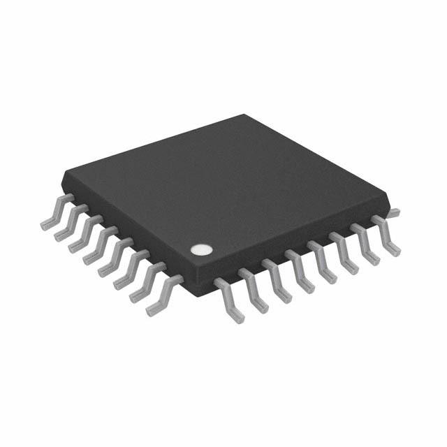
| 产品图片 |
|
| rohs | 符合RoHS无铅 / 符合限制有害物质指令(RoHS)规范要求 |
| 产品系列 | 数据转换器IC,模数转换器 - ADC,Maxim Integrated MAX157BEUA+- |
| 数据手册 | |
| 产品型号 | MAX157BEUA+ |
| 产品培训模块 | http://www.digikey.cn/PTM/IndividualPTM.page?site=cn&lang=zhs&ptm=25703http://www.digikey.cn/PTM/IndividualPTM.page?site=cn&lang=zhs&ptm=25705 |
| 产品种类 | 模数转换器 - ADC |
| 位数 | 10 |
| 供应商器件封装 | 8-uMAX |
| 信噪比 | Yes |
| 分辨率 | 10 bit |
| 包装 | 管件 |
| 商标 | Maxim Integrated |
| 安装类型 | 表面贴装 |
| 安装风格 | SMD/SMT |
| 封装 | Tube |
| 封装/外壳 | 8-TSSOP,8-MSOP(0.118",3.00mm 宽) |
| 封装/箱体 | UMAX-8 |
| 工作温度 | -40°C ~ 85°C |
| 工作电源电压 | 2.7 V to 5.25 V |
| 工厂包装数量 | 50 |
| 接口类型 | QSPI, Serial (SPI, Microwire) |
| 数据接口 | MICROWIRE™,QSPI™,串行,SPI™ |
| 最大功率耗散 | 330 mW |
| 最大工作温度 | + 85 C |
| 最小工作温度 | - 40 C |
| 标准包装 | 1 |
| 特性 | - |
| 电压参考 | 5.25 V |
| 电压源 | 单电源 |
| 系列 | MAX157B |
| 结构 | SAR |
| 转换器数 | 1 |
| 转换器数量 | 1 |
| 转换速率 | 108 kS/s |
| 输入数和类型 | 2 个单端,单极 |
| 输入类型 | Single-Ended |
| 通道数量 | 2 Channel |
| 采样率(每秒) | 108k |
| 零件号别名 | MAX157B |


- 商务部:美国ITC正式对集成电路等产品启动337调查
- 曝三星4nm工艺存在良率问题 高通将骁龙8 Gen1或转产台积电
- 太阳诱电将投资9.5亿元在常州建新厂生产MLCC 预计2023年完工
- 英特尔发布欧洲新工厂建设计划 深化IDM 2.0 战略
- 台积电先进制程称霸业界 有大客户加持明年业绩稳了
- 达到5530亿美元!SIA预计今年全球半导体销售额将创下新高
- 英特尔拟将自动驾驶子公司Mobileye上市 估值或超500亿美元
- 三星加码芯片和SET,合并消费电子和移动部门,撤换高东真等 CEO
- 三星电子宣布重大人事变动 还合并消费电子和移动部门
- 海关总署:前11个月进口集成电路产品价值2.52万亿元 增长14.8%


PDF Datasheet 数据手册内容提取
19-1388; Rev 0; 11/98 +2.7V, Low-Power, 2-Channel, 108ksps, Serial 10-Bit ADCs in 8-Pin µMAX General Description Features M The MAX157/MAX159 low-power, 10-bit analog-to-digi- 'Single-Supply Operation (+2.7V to +5.25V) A tal converters (ADCs) are available in 8-pin µMAX and DIP packages. Both devices operate with a single 'Two Single-Ended Channels (MAX157) X +2.7V to +5.25V supply and feature a 7.4µs succes- Single Pseudo-Differential Channel (MAX159) 1 sive-approximation ADC, automatic power-down, fast 'Low Power 5 wake-up (2.5µs), an on-chip clock, and a high-speed, 0.9mA (at 108ksps, +3V) 7 3-wire serial interface. 100µA(at 10ksps, +3V) / Power consumption is only 3.2mW (VDD= +3.6V) at the 10µA (at 1ksps, +3V) M maximum sampling rate of 108ksps. At slower through- <0.2µA (power-down mode) A put rates, the 0.2µA automatic shutdown further reduces power consumption. 'Internal Track/Hold X The MAX157 provides 2-channel, single-ended opera- '108ksps Sampling Rate 1 tion and accepts input signals from 0 to VREF. The 'SPI/QSPI/MICROWIRE-Compatible 3-Wire 5 MAX159 accepts pseudo-differential inputs ranging 9 from 0 to VREF. An external clock accesses data Serial Interface through the 3-wire serial interface, which is SPI™, 'Space-Saving 8-Pin µMAX Package QSPI™, and MICROWIRE™ compatible. 'Pin-Compatible 12-Bit Upgrades Available Excellent dynamic performance and low power, com- bined with ease of use and a small package size, make these converters ideal for battery-powered and data acquisition applications, or for other circuits with demanding power-consumption and space require- Ordering Information ments. For pin-compatible 12-bit upgrades, see the MAX144/MAX145 data sheet. TEMP. PIN- INL PART Applications RANGE PACKAGE (LSB) MAX157ACUA 0°C to +70°C 8 µMAX ±0.5 Battery-Powered Systems Instrumentation MAX157BCUA 0°C to +70°C 8 µMAX ±1 Portable Data Logging Test Equipment MAX157ACPA 0°C to +70°C 8 Plastic DIP ±0.5 Isolated Data Acquisition Medical Instruments MAX157BCPA 0°C to +70°C 8 Plastic DIP ±1 Process-Control Monitoring System Supervision MAX157AEUA -40°C to +85°C 8 µMAX ±0.5 MAX157BEUA -40°C to +85°C 8 µMAX ±1 MAX157AEPA -40°C to +85°C 8 Plastic DIP ±0.5 Pin Configuration MAX157BEPA -40°C to +85°C 8 Plastic DIP ±1 MAX157AMJA -55°C to +125°C 8 CERDIP* ±0.5 TOP VIEW MAX157BMJA -55°C to +125°C 8 CERDIP* ±1 MAX159ACUA 0°C to +70°C 8 µMAX ±0.5 VDD 1 8 SCLK MAX159BCUA 0°C to +70°C 8 µMAX ±1 CH0 (CH+) 2 7 DOUT MAX159ACPA 0°C to +70°C 8 Plastic DIP ±0.5 MAX157 MAX159BCPA 0°C to +70°C 8 Plastic DIP ±1 CH1 (CH-) 3 MAX159 6 CS/SHDN MAX159AEUA -40°C to +85°C 8 µMAX ±0.5 GND 4 5 REF MAX159BEUA -40°C to +85°C 8 µMAX ±1 MAX159AEPA -40°C to +85°C 8 Plastic DIP ±0.5 m MAX/DIP MAX159BEPA -40°C to +85°C 8 Plastic DIP ±1 ( ) ARE FOR MAX159 ONLY. MAX159AMJA -55°C to +125°C 8 CERDIP* ±0.5 MAX159BMJA -55°C to +125°C 8 CERDIP* ±1 SPI and QSPI are trademarks of Motorola, Inc. MICROWIRE is a trademark of National SemiconductorCorp. *Contact factory for availability. ________________________________________________________________Maxim Integrated Products 1 For free samples & the latest literature: http://www.maxim-ic.com, or phone 1-800-998-8800. For small orders, phone 1-800-835-8769.
+2.7V, Low-Power, 2-Channel, 108ksps, Serial 10-Bit ADCs in 8-Pin µMAX 9 ABSOLUTE MAXIMUM RATINGS 5 VDDto GND..............................................................-0.3V to +6V Operating Temperature Ranges 1 CH0, CH1 (CH+, CH-) to GND...................-0.3V to (VDD+ 0.3V) MAX157/MAX159_C_A.......................................0°C to +70°C X REF to GND................................................-0.3V to (VDD+ 0.3V) MAX157/MAX159_E_A....................................-40°C to +85°C Digital Inputs to GND...............................................-0.3V to +6V MAX157/MAX159_MJA.................................-55°C to +125°C A DOUT to GND.............................................-0.3V to (VDD+ 0.3V) Storage Temperature Range.............................-60°C to +150°C M DOUT Sink Current............................................................25mA Lead Temperature (soldering, 10sec).............................+300°C Continuous Power Dissipation (TA= +70°C) / µMAX (derate 4.1mW/°C above +70°C)......................330mW 7 Plastic DIP (derate 9.09mW/°C above +70°C)............727mW 5 CERDIP (derate 8.00mW/°C above +70°C).................640mW 1 Stresses beyond those listed under “Absolute Maximum Ratings” may cause permanent damage to the device. These are stress ratings only, and functional X operation of the device at these or any other conditions beyond those indicated in the operational sections of the specifications is not implied. Exposure to absolute maximum rating conditions for extended periods may affect device reliability. A M ELECTRICAL CHARACTERISTICS (VDD = +2.7V to +5.25V, VREF = 2.5V, 0.1µF capacitor at REF, fSCLK = 2.17MHz, 16 clocks/conversion cycle (108ksps), CH- = GND for MAX159, TA= TMINto TMAX, unless otherwise noted. Typical values are at TA= +25°C.) PARAMETER SYMBOL CONDITIONS MIN TYP MAX UNITS DC ACCURACY (Note 1) Resolution RES 10 Bits MAX15_A ±0.5 Relative Accuracy (Note 2) INL LSB MAX15_B ±1 Differential Nonlinearity DNL No missing codes over temperature ±0.5 LSB Offset Error ±2 LSB Gain Error (Note 3) ±2 LSB Gain Temperature Coefficient External reference, VREF= 2.5V ±0.8 ppm/°C Channel-to-Channel Offset ±0.02 LSB Matching Channel-to-Channel Gain ±0.02 LSB Matching DYNAMIC SPECIFICATIONS(fIN (sine wave) = 10kHz, VIN= 2.5Vp-p, 108ksps, external fSCLK= 2.17MHz, CH- = GND for MAX159) Signal-to-Noise Ratio plus SINAD 66 dB Distortion Total Harmonic Distortion THD -70 dB (including 5th-order harmonic) Spurious-Free Dynamic Range SFDR 70 dB Channel-to-Channel Crosstalk fIN= 65kHz, VIN= 2.5Vp-p (Note 4) -75 dB Small-Signal Bandwidth -3dB rolloff 2.25 MHz Full-Power Bandwidth 1.0 MHz 2 _______________________________________________________________________________________
+2.7V, Low-Power, 2-Channel, 108ksps, Serial 10-Bit ADCs in 8-Pin µMAX ELECTRICAL CHARACTERISTICS (continued) M (VDD = +2.7V to +5.25V, VREF = 2.5V, 0.1µF capacitor at REF, fSCLK = 2.17MHz, 16 clocks/conversion cycle (108ksps), A CH- = GND for MAX159, TA= TMINto TMAX, unless otherwise noted. Typical values are at TA= +25°C.) X PARAMETER SYMBOL CONDITIONS MIN TYP MAX UNITS 1 CCOONNVVEERRSSIIOONN RRAATTEE 5 External clock, fSCLK= 2.17MHz, 16 clock 7.4 7 Conversion Time (Note 5) tCONV cycles per conversion µs / Internal clock 5 7 M T/H Acquisition Time tACQ 2.5 µs A Aperture Delay 25 ns X Aperture Jitter <50 ps 1 External clock mode 0.1 2.17 MHz Serial Clock Frequency fSCLK MHz 5 Internal clock mode, for data transfer only 0 5 9 ANALOG INPUTS Analog Input Voltage Range (Note 6) VIN 0 VREF V Multiplexer Leakage Current On/off-leakage current, VIN= 0 to VDD ±0.01 ±1 µA Input Capacitance CIN 16 µA EXTERNAL REFERENCE Input Voltage Range (Note 7) VREF 0 VDD + 50mV V Input Current VREF= 2.5V 100 140 µA Input Resistance 18 25 kΩ Shutdown REF Input Current 0.01 10 µA DIGITAL INPUTS (CS/SHDN, SCLK) AND DIGITAL OUTPUT (DOUT) VDD≤3.6V 2.0 Input High Voltage VIH V VDD> 3.6V 3.0 Input Low Voltage VIL 0.8 V Input Hysteresis VHYS 0.2 V Input Leakage Current IIN VIN= 0 or VDD ±1 µA Input Capacitance CIN (Note 8) 15 pF ISINK= 5mA 0.4 Output Low Voltage VOL V ISINK= 16mA 0.5 Output High Voltage VOH ISOURCE= 0.5mA VDD- 0.5 V Three-State Output Leakage Current CS/SHDN = VDD ±10 µA Three-State Output Capacitance COUT CS/SHDN = VDD(Note 8) 15 pF _______________________________________________________________________________________ 3
+2.7V, Low-Power, 2-Channel, 108ksps, Serial 10-Bit ADCs in 8-Pin µMAX 9 ELECTRICAL CHARACTERISTICS (continued) 5 (VDD = +2.7V to +5.25V, VREF = 2.5V, 0.1µF capacitor at REF, fSCLK = 2.17MHz, 16 clocks/conversion cycle (108ksps), 1 CH- = GND for MAX159, TA= TMINto TMAX, unless otherwise noted. Typical values are at TA= +25°C.) X PARAMETER SYMBOL CONDITIONS MIN TYP MAX UNITS A PPOOWWEERR RREEQQUUIIRREEMMEENNTTSS M Positive Supply Voltage VDD +2.7 +5.25 V / Positive Supply Current IDD Operating mode 0.9 2.0 mA 7 Positive Supply Current IDD Shutdown, CS/SHDN = GND 0.2 5 µA 5 Power-Supply Rejection 1 (Note 9) PSR VDD= 2.7V to 5.25V, full-scale input ±0.15 mV X A TIMING CHARACTERISTICS (Figure 7) M (VDD = +2.7V to +5.25V, VREF = 2.5V, 0.1µF capacitor at REF, fSCLK = 2.17MHz, 16 clocks/conversion cycle (108ksps), CH- = GND for MAX159, TA= TMINto TMAX, unless otherwise noted. Typical values are at TA= +25°C.) PARAMETER SYMBOL CONDITIONS MIN TYP MAX UNITS Wake-Up Time tWAKE 2.5 µs CS/SHDNFall to Output Enable tDV CL= 100pF (Figure 1) 120 ns CS/SHDN Rise to Output tTR CL = 100pF (Figure 1) 120 ns Disable SCLK Fall to Output Data Valid tDO CL= 100pF 20 120 ns External clock 0.1 2.17 SCLK Clock Frequency fSCLK MHz Internal clock, SCLK for data transfer only 0 5 External clock 215 SCLK Pulse Width High tCH Internal clock, SCLK for data transfer only ns 50 (Note 8) External clock 215 SCLK Pulse Width Low tCL Internal clock, SCLK for data transfer only ns 50 (Note 8) SCLK to CS/SHDN Setup tSCLKS 60 ns CS/SHDN Pulse Width tCS 60 ns Note 1: Tested at VDD= +2.7V. Note 2: Relative accuracy is the deviation of the analog value at any code from its theoretical value after full-scale range has been calibrated. Note 3: Offset nulled. Note 4: The on channel is grounded; the sine wave is applied to off channel (MAX157 only). Note 5: Conversion time is defined as the number of clock cycles times the clock period; clock has 50% duty cycle. Note 6: The common-mode range for the analog inputs is from GND to VDD(MAX159 only). Note 7: ADC performance is limited by the converter’s noise floor, typically 300µVp-p. Note 8: Guaranteed by design. Not subject to production testing. Note 9: Measured as VFS(2.7V) - VFS(5.25V). 4 _______________________________________________________________________________________
+2.7V, Low-Power, 2-Channel, 108ksps, Serial 10-Bit ADCs in 8-Pin µMAX Typical Operating Characteristics M (VDD= +3.0V, VREF= 2.5V, 0.1µF capacitor at REF, fSCLK= 2.17MHz, 16 clocks/conversion cycle (108ksps); CH- = GND for A MAX159; TA = +25°C, unless otherwise noted.) X SUPPLY CURRENT SUPPLY CURRENT SUPPLY CURRENT 1 vs. SUPPLY VOLTAGE vs. TEMPERATURE vs. SAMPLING RATE 5 A)11350000 CVRCRLLO E =D=F E¥5= 0 =Vp 1DF0D10101000 MAX157/159 toc01 A)11255000 CCVRRLLO E =D=F E¥5= 0 =Vp 1DF0D10101000 MAX157/159 toc02 A)101,000000 VCCRLOE D=F E5= 0 =Vp 1DF0D1 0101000 MAX157/159 toc03 7/M mSUPPLY CURRENT (1910000 mSUPPLY CURRENT (1705000 mSUPPLY CURRENT ( 10100 AX15 700 1 9 500 500 0.1 2.5 3.0 3.5 4.0 4.5 5.0 5.5 -60 -40 -20 0 20 40 60 80 100 120 140 0.1 1 10 100 1k 10k 100k VDD (V) TEMPERATURE (°C) SAMPLING RATE (sps) SHUTDOWN CURRENT SHUTDOWN CURRENT vs. SUPPLY VOLTAGE vs. TEMPERATURE 1000 1000 A) 800 VREF = VDD MAX157/159 toc04 A) 800 VREF = VDD MAX157/159 toc05 NT (n NT (n RE 600 RE 600 R R U U C C N N W W O 400 O 400 D D UT UT H H S S 200 200 0 0 2.5 3.0 3.5 4.0 4.5 5.0 5.5 -60 -40 -20 0 20 40 60 80 100 120 140 VDD (V) TEMPERATURE (°C) OFFSET ERROR vs. SUPPLY VOLTAGE OFFSET ERROR vs. TEMPERATURE 00..1250 MAX157/159 toc06 00..1250 MAX157/159 toc07 OR (LSB) OR (LSB) OFFSET ERR0.10 OFFSET ERR 0.10 0.05 0.05 0 0 2.5 3.0 3.5 4.0 4.5 5.0 5.5 -60 -35 -10 15 40 65 90 115 140 VDD (V) TEMPERATURE (°C) _______________________________________________________________________________________ 5
+2.7V, Low-Power, 2-Channel, 108ksps, Serial 10-Bit ADCs in 8-Pin µMAX 9 Typical Operating Characteristics (continued) 5 (VDD= +3.0V, VREF= 2.5V, 0.1µF capacitor at REF, fSCLK= 2.17MHz, 16 clocks/conversion cycle (108ksps); CH- = GND for 1 MAX159; TA = +25°C, unless otherwise noted.) X GAIN ERROR GAIN ERROR INTEGRAL NONLINEARITY A vs. SUPPLY VOLTAGE vs. TEMPERATURE vs. OUTPUT CODE 7/M 00..21 MAX157/159 toc08 00..12 MAX157/159 toc09 00..0023 MAX157/8 toc10 AX15 GAIN ERROR (LSB) 0 GAIN ERROR (LSB) 0 INL (LSB)-00..00011 M -0.1 -0.1 -0.02 -0.2 -0.2 -0.03 2.5 3.0 3.5 4.0 4.5 5.0 5.5 -60 -35 -10 15 40 65 90 115 140 0 250 500 750 1000 VDD (V) TEMPERATURE (°C) OUTPUT CODE INTEGRAL NONLINEARITY INTEGRAL NONLINEARITY vs. SUPPLY VOLTAGE vs. TEMPERATURE 00..1250 MAX157/159 toc11 00..1250 MAX157/159 toc12 B) B) S S NL (L0.10 NL (L0.10 I I 0.05 0.05 0 0 2.5 3.0 3.5 4.0 4.5 5.0 5.5 -60 -35 -10 15 40 65 90 115 140 VDD (V) TEMPERATURE (°C) 6 _______________________________________________________________________________________
+2.7V, Low-Power, 2-Channel, 108ksps, Serial 10-Bit ADCs in 8-Pin µMAX Pin Description M PIN NAME FUNCTION A 1 VDD Positive Supply Voltage, +2.7V to +5.25V X 2 CH0 (CH+) Analog Input, MAX157: Single-Ended (CH0); MAX159: Differential (CH+). 1 3 CH1 (CH-) Analog Input, MAX157: Single-Ended (CH1); MAX159: Differential (CH-). 5 4 GND Analog and Digital Ground 7 External Reference Voltage Input. Sets analog voltage range. Bypass with a 100nF capacitor close to the / 5 REF M part. Active-Low Chip-Select Input, Active-High Shutdown Input. Pulling CS/SHDN high puts chip into A 6 CS/SHDN shutdown with a maximum current of 5µA. X 7 DOUT Serial Data Output. Data changes state at SCLK’s falling edge. High impedance when CS/SHDN is high. 1 8 SCLK Serial Clock Input. DOUT changes on the falling edge of SCLK. 5 9 VDD DOUT 6k DOUT 6k CL CL GND GND a) HIGH-Z TO V0H, V0L TO V0H, AND VOH TO HIGH-Z b) HIGH-Z TO V0L, V0H TO V0L, AND VOL TO HIGH-Z Figure 1. Load Circuits for Enable and Disable Time Detailed Description the same channel by toggling CS/SHDN twice between conversions. If only one channel is required, CH0 and The MAX157/MAX159 analog-to-digital converters CH1 may be connected together; however the output (ADCs) use a successive-approximation conversion data will still contain the channel identification bit (SAR) technique and on-chip track/hold (T/H) structure (before the MSB). to convert an analog signal to a serial, 10-bit digital out- put data stream. For the MAX159, the input channels form a single differ- ential channel pair (CH+, CH-). This configuration is This flexible serial interface provides easy interface to pseudo-differential to the effect that only the signal at microprocessors (µPs). Figure 2 shows a simplified IN+ is sampled. The return side IN- must remain stable functional diagram of the internal architecture for both within ±0.5LSB (±0.1LSB for optimum results) with the MAX157 (2 channels, single-ended) and the respect to GND during a conversion. To accomplish MAX159 (1 channel, pseudo-differential). this, connect a 0.1µF capacitor from IN- to GND. Single-Ended (MAX157) and Pseudo- During the acquisition interval, the channel selected as Differential (MAX159) Analog Inputs the positive input (IN+) charges capacitor CHOLD. The The sampling architecture of the ADC’s analog com- acquisition interval spans from when CS/SHDN falls to parator is illustrated in the equivalent input circuit in the falling edge of the second clock cycle (external Figure 3. In single-ended mode (MAX157), both chan- clock mode) or from when CS/SHDN falls to the first nels CH0 and CH1 are referred to GND and can be falling edge of SCLK (internal clock mode). At the end connected to two different signal sources. Following the of the acquisition interval, the T/H switch opens, retain- power-on reset, the ADC is set to convert CH0. After ing charge on CHOLDas a sample of the signal at IN+. CH0 has been converted, CH1 will be converted, and The conversion interval begins with the input multiplex- the conversions will continue to alternate between er switching CHOLD from the positive input (IN+) to the channels. Channel switching is performed by toggling negative input (IN-). This unbalances node ZERO at the the CS/SHDN pin. Conversions can be performed on comparator’s positive input. _______________________________________________________________________________________ 7
+2.7V, Low-Power, 2-Channel, 108ksps, Serial 10-Bit ADCs in 8-Pin µMAX 9 The capacitive digital-to-analog converter (DAC) Higher source impedances can be used if a 0.01µF 5 adjusts during the remainder of the conversion cycle capacitor is connected to the individual analog inputs. to restore node ZERO to 0V within the limits of 10-bit Together with the input impedance, this capacitor forms 1 resolution. This action is equivalent to transferring a an RC filter, limiting the ADC’s signal bandwidth. X 16pF · [(VIN+) - (VIN-)] charge from CHOLD to the bina- A ry-weighted capacitive DAC, which in turn forms a digi- Input Bandwidth The MAX157/MAX159 T/H stage offers both a 2.25MHz M tal representation of the analog input signal. small-signal and a 1MHz full-power bandwidth, which / Track/Hold makes it possible to use the parts for digitizing high- 7 The ADC’s T/H stage enters its tracking mode on the speed transients and measuring periodic signals with 5 falling edge of CS/SHDN. For the MAX157 (single- bandwidths exceeding the ADC’s sampling rate by 1 ended inputs), IN- is connected to GND and the con- using undersampling techniques. To avoid high-fre- X verter samples the positive (“+”) input. For the MAX159 quency signals being aliased into the frequency band (pseudo-differential inputs), IN- connects to the nega- of interest, anti-alias filtering is recommended. Most A tive input (“-”), and the difference of [(VIN+) - (VIN-)] is aliasing problems can be fixed easily with an external M sampled. At the end of the conversion, the positive resistor and a capacitor. However, if DC precision is input connects back to IN+ and CHOLD charges to the required, it is usually best to choose a continuous input signal. or switched-capacitor filter, such as the MAX7410/ MAX7414 (Figure 4). Their Butterworth characteristic The time required for the T/H stage to acquire an input generally provides the best compromise (with regard to signal is a function of how fast its input capacitance is rolloff and attenuation) in filter configurations, is easy to charged. If the input signal’s source impedance is high, design, and provides a maximally flat passband re- the acquisition time lengthens and more time must be sponse. allowed between conversions. The acquisition time, tACQ, is the maximum time the device takes to acquire Analog Input Protection the signal, and is also the minimum time required for Internal protection diodes, which clamp the analog the signal to be acquired. Calculate this with the follow- input to VDD and GND, allow each input channel to ing equation: swing within GND - 300mV to VDD + 300mV without damage. However, for accurate conversions both tACQ= 7(RS+ RIN)CIN inputs must not exceed VDD + 50mV or be less than where RS is the source impedance of the input signal, GND - 50mV. RIN (9kΩ) is the input resistance, and CIN (16pF) is the If an off-channel analog input voltage exceeds the input capacitance of the ADC. Source impedances supplies, limit the input current to 4mA. below 4kΩhave no significant impact on the AC perfor- mance of the MAX157/MAX159. CAPACITIVE DAC CS/SHDN REF SCLK INPUT COMPARATOR INTERNAL CH1 MUX – + ZERO CLOCK (CH-) COLONGTRICOL ROEUGTISPTUETR DOUT CH0 C16HpOFLD RIN TO SAR (CH+) 9k CH0 CSWITCH (CH+) SCLK TRACK HOLD ANALOG 10+2 BIT INPUT T/H IN SAR OUT MAX157 CH1 MUX ADC T/H (CH-) (2 CHANNEL) MAX159 CONTROL GND LOGIC REF SINGLE-ENDED MODE: CHO, CH1 = IN+; GND = IN- ( ) ARE FOR MAX159 DIFFERENTIAL MODE: CH+ = IN+; CH- = IN- ( ) ARE FOR MAX159 Figure 2. MAX157/MAX159 Simplified Functional Diagram Figure 3. Analog Input Channel Structure 8 _______________________________________________________________________________________
+2.7V, Low-Power, 2-Channel, 108ksps, Serial 10-Bit ADCs in 8-Pin µMAX Selecting Clock Mode ing SCLK high during a high/low transition of CS/SHDN. M To start the conversion process on the MAX157/ The first SCLK falling edge samples the data and initi- MAX159, pull CS/SHDN low. At CS/SHDN’s falling ates a conversion using the integrated on-chip oscilla- A edge, the part wakes up, the internal T/H enters track tor. After the conversion, the oscillator shuts off and X mode, and a conversion begins. In addition, the state of DOUT goes high, signaling the end of conversion 1 SCLK at CS/SHDN’s falling edge selects internal (SCLK (EOC). Data can then be read out with SCLK. 5 = high) or external (SCLK = low) clock mode. External Clock (fSCLK= 100kHz to 2.17MHz) 7 Internal Clock (fSCLK< 100kHz or fSCLK> 2.17MHz) External clock mode (Figure 6) is selected by transition- / In internal clock mode, the MAX157/MAX159 run from ing CS/SHDN from high to low while SCLK is low. The M an internal, laser-trimmed oscillator to within 20% of the external clock signal not only shifts data out, but also A 2MHz specified clock rate. This releases the system drives the analog-to-digital conversion. The input is microprocessor from running the SAR conversion clock sampled and conversion begins on the falling edge of X and allows the conversion results to be read back at the the second clock pulse. Conversion must be completed 1 processor’s convenience, at any clock rate from 0 to within 140µs to prevent degradation in the conversion 5 5MHz. Operating the MAX157/MAX159 in internal clock results caused by droop on the T/H capacitors. External 9 mode is necessary for serial interfaces operating with clock mode provides the best throughput for clock fre- clock frequencies lower than 100kHz or greater than quencies between 100kHz and 2.17MHz. 2.17MHz. Select internal clock mode (Figure 5) by hold- VDD 4 1 VDD SHDN 7 0.1m F 2 CH0 VDD REF 5 EXTERNAL REFERENCE 470W 5 MAX7410 OUT MAX157 2 IN MAX7414 CLK 8 3 CH1 DOUT 7 fCORNER = 15kHz 0.01m F 8 6 SCLK CS/SHDN m P/m C COM OS GND GND 1 6 3 4 0.01m F 1.5MHz CLOCK Figure 4. Analog Input with Anti-Aliasing Filter Structure ACTIVE POWER ACTIVE DOWN tWAKE tCONV tCS (tACQ) CS/SHDN SCLK 1 2 3 4 5 6 7 8 9 10 11 12 13 14 15 16 HIGH-Z EOC 1 1 CHID MSB D8 D7 D6 D5 D4 D3 D2 D1 D0 S1 S0 DOUT HIGH-Z SAMPLING INSTANT Figure 5. Internal Clock Mode Timing _______________________________________________________________________________________ 9
+2.7V, Low-Power, 2-Channel, 108ksps, Serial 10-Bit ADCs in 8-Pin µMAX 9 Output Data Format Automatic Power-Down Mode 5 Table 1 illustrates the 16-bit, serial data-stream output Whenever the MAX157/MAX159 are not selected 1 format for both the MAX157 and MAX159. The first three (CS/SHDN = VDD), the parts enter their shutdown mode. bits are always logic high (including the EOC bit for In shutdown all internal circuitry is turned off, which X internal clock mode), followed by the channel identifica- reduces the supply current to typically less than 0.2µA. A tion (CHID = 0 for CH0, CHID = 1 for CH1, CHID = 1 for With an external reference stable to within 1LSB, the M MAX159), the 10 bits of data in MSB first format, and wake-up time is 2.5µs. If the external reference is not sta- two sub-LSB bits (S1 and S0). After the last bit has been ble within 1LSB, the wake-up time must be increased to / read out, additional SCLK pulses will clock out trailing allow the reference to stabilize. 7 zeros. DOUT transitions on the falling edge of SCLK. 5 Applications Information The output remains high impedance when CS/SHDN is 1 high. Signal-to-Noise Ratio (SNR) X External Reference For a waveform perfectly reconstructed from digital A samples, SNR is the ratio of full-scale analog input An external reference is required for both the MAX157 (RMS value) to the RMS quantization error (residual M and MAX159. At REF, the DC input resistance is a mini- mum of 18kΩ. During a conversion, a reference must error). The ideal, theoretical minimum analog-to-digital noise is caused by quantization error only and results be able to deliver 250µA of DC load current and have an output impedance of 10Ω or less. Use a 0.1µF directly from the ADC’s resolution (N bits): bypass capacitor for best performance. The reference SNR(MAX)= (6.02 ·N + 1.76)dB input structure allows a voltage range of 0 to (VDD + 50mV) although noise levels will decrease effective res- In reality, there are other noise sources besides quanti- olution at lower reference voltages. zation noise: thermal noise, reference noise, clock jitter, ACTIVE POWER ACTIVE DOWN SAMPLING INSTANT tWAKE tCS (tACQ) CS/SHDN SCLK 1 2 3 4 5 6 7 8 9 10 11 12 13 14 15 16 HIGH-Z HIGH-Z CHID MSB D8 D7 D6 D5 D4 D3 D2 D1 D0 S1 S0 DOUT Figure 6. External Clock Mode Timing CS/SHDN • • • tSCLKS tCH tCS tCL SCLK • • • tDV tDO tTR HIGH-Z HIGH-Z DOUT • • • Figure 7. Detailed Serial-Interface Timing Sequence 10 ______________________________________________________________________________________
+2.7V, Low-Power, 2-Channel, 108ksps, Serial 10-Bit ADCs in 8-Pin µMAX Table 1. Serial Output Data Stream for Internal and External Clock Mode M SCLK CYCLE 1 2 3 4 5 6 7 8 9 10 11 12 13 14 15 16 A DOUT (Internal Clock) EOC 1 1 CHID D9 D8 D7 D6 D5 D4 D3 D2 D1 D0 S1 S0 X DOUT (External Clock) 1 1 1 CHID D9 D8 D7 D6 D5 D4 D3 D2 D1 D0 S1 S0 1 5 etc. Therefore, SNR is computed by taking the ratio of serial clock for the MAX157/MAX159. Select a clock fre- 7 the RMS signal to the RMS noise (which includes all quency from 100kHz to 2.17MHz (external clock mode). / spectral components minus the fundamental), the first 1) Use a general-purpose I/O line on the CPU to pull M five harmonics, and the DC offset. CS/SHDN low while SCLK is low. A Signal-to-Noise Plus Distortion (SINAD) 2) Wait for the minimum wake-up time (tWAKE) speci- X Signal-to-noise plus distortion is the ratio of the funda- fied before activating SCLK. mental input frequency’s RMS amplitude to RMS equiv- 1 3) Activate SCLK for a minimum of 16 clock cycles. The alent of all other ADC output signals: first falling clock edge will generate a serial data- 5 (cid:215) Ø Signal ø stream of three leading ones, followed by the chan- 9 SINAD(dB) = 20 log Œ RMS œ nel identification, the MSB of the digitized input º (Noise + Distortion) ß RMS signal, and two sub-bits. DOUT transitions on SCLK’s falling edge and is available in MSB-first for- Effective Number of Bits (ENOB) mat. Observe the SCLK to DOUT valid timing char- ENOB indicates the global accuracy of an ADC at a acteristic. Data should be clocked into the µP on specific input frequency and sampling rate. An ideal SCLK’s rising edge. ADC’s error consists of quantization noise only. With an 4) Pull CS/SHDN high at or after the 16th falling clock input range equal to the full-scale range of the ADC, edge. If CS/SHDN remains low, trailing zeros will be calculate the effective number of bits as follows: clocked out after the sub-bits. ENOB = (SINAD - 1.76) / 6.02 5) With CS/SHDN high, wait at least 60ns (tCS), before starting a new conversion by pulling CS/SHDN low. Total Harmonic Distortion (THD) A conversion can be aborted by pulling CS/SHDN THD is the ratio of the RMS sum of the first five harmon- high before the conversion ends; wait at least 60ns ics of the input signal to the fundamental itself. This is before starting a new conversion. expressed as: Data can be output either in two 8-bit sequences or (cid:230) ( )(cid:246) continuously. The bytes will contain the result of the (cid:215) (cid:231) V22+ V32+ V42+ V52 (cid:247) conversion padded with three leading ones, the chan- THD = 20 log (cid:231) (cid:247) nel identification before the MSB, and two trailing sub- (cid:231) V12 (cid:247) bits. If the serial clock hasn’t been idled after the last Ł ł sub-bit (S0) and CS/SHDN is kept low, DOUT sends trailing zeros. where V1 is the fundamental amplitude and V2 through V5 are the amplitudes of the 2nd through 5th-order har- SPI and MICROWIRE Interface monics. When using SPI (Figure 8a) or MICROWIRE (Figure 8b) interfaces, set CPOL = 0 and CPHA = 0. Conversion Spurious-Free Dynamic Range (SFDR) begins with a falling edge on CS/SHDN (Figure 8c). Two SFDR is the ratio of RMS amplitude of the fundamental consecutive 8-bit readings are necessary to obtain the (maximum signal component) to the RMS value of the entire 10-bit result from the ADC. DOUT data transitions next largest spurious component, excluding DC offset. on the serial clock’s falling edge and is clocked into the µP on SCLK’s rising edge. The first 8-bit data stream Connection to Standard Interfaces contains three leading ones, followed by channel identi- The MAX157/MAX159 interface is fully compatible with fication and the first four data bits starting with the MSB. SPI/QSPI and MICROWIRE standard serial interfaces. The second 8-bit data stream contains the remaining If a serial interface is available, establish the CPU’s seri- bits, D5 through D0, and the sub-bits S1 and S0. al interface as master so that the CPU generates the ______________________________________________________________________________________ 11
+2.7V, Low-Power, 2-Channel, 108ksps, Serial 10-Bit ADCs in 8-Pin µMAX 9 5 I/O CS/SHDN I/O CS/SHDN 1 SCK SCLK SK SCLK X MISO DOUT SI DOUT A SPI VDD MICROWIRE M MAX157 MAX157 MAX159 MAX159 / SS 7 5 Figure 8a. SPI Connections Figure 8b. MICROWIRE Connections 1 X A M 1ST BYTE READ 2ND BYTE READ SCLK 1 2 3 4 5 6 7 8 9 10 11 12 13 14 15 16 CS/SHDN HIGH-Z DOUT* CHID D9 D8 D7 D6 D5 D4 D3 D2 D1 D0 S1 S0 SAMPLING MSB LSB INSTANT *WHEN CS/SHDN IS HIGH, DOUT = HIGH -Z Figure 8c. SPI/MICROWIRE Interface Timing Sequence (CPOL = CPHA = 0) QSPI Interface Using the high-speed QSPI interface with CPOL = 0 and CPHA = 0, the MAX157/MAX159 supports a maxi- CS CS/SHDN mum fSCLK of 2.17MHz. The QSPI circuit in Figure 9a can be programmed to perform a conversion on each SCK SCLK of the two channels for the MAX157. MISO DOUT Figure 9b shows the QSPI interface timing. QSPI VDD MAX157 PIC16 with SSP Module MAX159 SS and PIC17 Interface The MAX157/MAX159 are compatible with a PIC16/ PIC17 microcontroller (µC), using the synchronous seri- al port (SSP) module. Figure 9a. QSPI Connections To establish SPI communication, connect the controller three leading ones, the channel identification, and the as shown in Figure 10a and configure the PIC16/PIC17 first four data bits starting with the MSB. The second 8- as system master by initializing its synchronous serial bit data stream contains the remaining bits, D5 through port control register (SSPCON) and synchronous serial D0, and the two sub-bits S1 and S0. port status register (SSPSTAT) to the bit patterns shown in Tables 2 and 3. Layout, Grounding, and Bypassing In SPI mode, the PIC16/PIC17 µCs allow eight bits of For best performance use printed circuit boards data to be synchronously transmitted and received (PCBs), wire-wrap configurations are not recommend- simultaneously. Two consecutive 8-bit readings (Figure ed, since the layout should ensure proper separation of 10b) are necessary to obtain the entire 10-bit result analog and digital traces. Run analog and digital lines from the ADC. DOUT data transitions on the serial anti-parallel to each other, and don’t layout digital sig- clock’s falling edge and is clocked into the µC on nal paths underneath the ADC package. Use separate SCLK’s rising edge. The first 8-bit data stream contains analog and digital PCB ground sections with only one 12 ______________________________________________________________________________________
+2.7V, Low-Power, 2-Channel, 108ksps, Serial 10-Bit ADCs in 8-Pin µMAX M SCLK 1 2 3 4 5 6 7 8 9 10 11 12 13 14 15 16 A CS/SHDN X HIGH-Z 1 DOUT CHID D9 D8 D7 D6 D5 D4 D3 D2 D1 D0 S1 S0 5 SAMPLING INSTANT MSB LSB 7 *WHEN CS/SHDN IS HIGH, DOUT = HIGH - Z / M Figure 9b. QSPI Interface Timing Sequence (CPOL = CPHA = 0) A star-point (Figure 11) connecting the two ground sys- VDD VDD tems (analog and digital). For lowest-noise operation, X ensure the ground return to the star ground’s power 1 supply is low impedance and as short as possible. SCLK SCK 5 Route digital signals far away from sensitive analog and DOUT SDI 9 reference inputs. CS/SHDN I/O High-frequency noise in the power supply (VDD) could influence the proper operation of the ADC’s fast com- MAX157 PIC16/PIC17 parator. Bypass VDD to the star ground with a network MAX159 of two parallel capacitors, 0.1µF and 1µF, located as close as possible to the power supply pin of the GND GND MAX157/MAX159. Minimize capacitor lead length for best supply-noise rejection and add an attenuation Figure 10a. SPI Interface Connection for a PIC16/PIC17 resistor (10Ω) if the power supply is extremely noisy. Controller 1ST BYTE READ 2ND BYTE READ SCLK 1 2 3 4 5 6 7 8 9 10 11 12 13 14 15 16 CS/SHDN HIGH-Z DOUT* CHID D9 D8 D7 D6 D5 D4 D3 D2 D1 D0 S1 S0 SAMPLING INSTANT MSB LSB *WHEN CS/SHDN IS HIGH, DOUT = HIGH - Z Figure 10b. SPI Interface Timing Sequence with PIC16/17 in Master Mode (CKE = 1, CKP = 0, SMP = 0, SSPM3–SSPM0 = 0001) POWER SUPPLIES +3V +3V GND R* = 10W 1m F 0.1m F VDD GND +3V DGND DIGITAL MAX157 CIRCUITRY MAX159 * OPTIONAL FILTER RESISTOR Figure 11. Power-Supply Bypassing and Grounding ______________________________________________________________________________________ 13
+2.7V, Low-Power, 2-Channel, 108ksps, Serial 10-Bit ADCs in 8-Pin µMAX 9 Table 2. Detailed SSPCON Register Content 5 MAX157/MAX159 1 CONTROL BIT SYNCHRONOUS SERIAL PORT CONTROL REGISTER (SSPCON) SETTINGS X WCOL Bit 7 X Write Collision Detection Bit A SSPOV Bit 6 X Receive Overflow Detect Bit M Synchronous Serial Port Enable Bit / SSPEN Bit 5 1 0: Disables serial port and configures these pins as I/O port pins. 7 1: Enables serial port and configures SCK, SDO and SCI pins as serial port pins. 5 CKP Bit 4 0 Clock Polarity Select Bit. CKP = 0 for SPI master mode selection. 1 SSPM3 Bit 3 0 X A SSPM2 Bit 2 0 Synchronous Serial Port Mode Select Bit. Sets SPI master mode and selects SSPM1 Bit 1 0 fCLK= fOSC/ 16. M SSPM0 Bit 0 1 X = Don’t care Table 3. Detailed SSPSTAT Register Content MAX157/MAX159 CONTROL BIT SYNCHRONOUS SERIAL STATUS REGISTER (SSPSTAT) SETTINGS SPI Data Input Sample Phase. Input data is sampled at the middle of the data output SMP Bit 7 0 time. CKE Bit 6 1 SPI Clock Edge Select Bit. Data will be transmitted on the rising edge of the serial clock. D/A Bit 5 X Data Address Bit P Bit 4 X Stop Bit S Bit 3 X Start Bit R/W Bit 2 X Read/Write Bit Information UA Bit 1 X Update Address BF Bit 0 X Buffer Full Status Bit X = Don’t care 14 ______________________________________________________________________________________
+2.7V, Low-Power, 2-Channel, 108ksps, Serial 10-Bit ADCs in 8-Pin µMAX Chip Information M TRANSISTOR COUNT: 2,058 A SUBSTRATE CONNECTED TO GND X 1 5 7 / M A Package Information X 1 S P E 5 D. AX 9 M U L 8 ______________________________________________________________________________________ 15
+2.7V, Low-Power, 2-Channel, 108ksps, Serial 10-Bit ADCs in 8-Pin µMAX 9 Package Information (continued) 5 1 X PDIPN.EPS A M / 7 5 1 X A M Maxim cannot assume responsibility for use of any circuitry other than circuitry entirely embodied in a Maxim product. No circuit patent licenses are implied. Maxim reserves the right to change the circuitry and specifications without notice at any time. 16 ____________________Maxim Integrated Products, 120 San Gabriel Drive, Sunnyvale, CA 94086 408-737-7600 © 1998 Maxim Integrated Products Printed USA is a registered trademark of Maxim Integrated Products.
Mouser Electronics Authorized Distributor Click to View Pricing, Inventory, Delivery & Lifecycle Information: M axim Integrated: MAX157BEUA+T MAX157ACPA+ MAX157ACUA+ MAX157ACUA+T MAX157AEPA+ MAX157AEUA+ MAX157AEUA+T MAX157BCPA+ MAX157BCUA+ MAX157BCUA+T MAX157BEPA+ MAX157BEUA+ MAX159ACPA+ MAX159ACUA+ MAX159AEPA+ MAX159AEUA+ MAX159AEUA+T MAX159BCPA+ MAX159BCUA+ MAX159BCUA+T MAX159BEPA+ MAX159BEUA+ MAX159BEUA+T MAX159ACUA+T