ICGOO在线商城 > 集成电路(IC) > PMIC - 稳压器 - 线性 > MAX15027ATB+T

 Datasheet下载
- 型号: MAX15027ATB+T
- 制造商: Maxim
- 库位|库存: xxxx|xxxx
- 要求:
| 数量阶梯 | 香港交货 | 国内含税 |
| +xxxx | $xxxx | ¥xxxx |
查看当月历史价格
查看今年历史价格
MAX15027ATB+T产品简介:
ICGOO电子元器件商城为您提供MAX15027ATB+T由Maxim设计生产,在icgoo商城现货销售,并且可以通过原厂、代理商等渠道进行代购。 MAX15027ATB+T价格参考¥16.55-¥28.49。MaximMAX15027ATB+T封装/规格:PMIC - 稳压器 - 线性, Linear Voltage Regulator IC Positive Adjustable 1 Output 0.5 V ~ 3.3 V 1A 10-TDFN-EP (3x3)。您可以下载MAX15027ATB+T参考资料、Datasheet数据手册功能说明书,资料中有MAX15027ATB+T 详细功能的应用电路图电压和使用方法及教程。
MAX15027ATB+T 是 Maxim Integrated 生产的一款 PMIC(电源管理集成电路),属于线性稳压器类别。它主要应用于需要高效、低噪声、高精度电压调节的场景中,特别适合对电源要求严格的便携式和电池供电设备。

 主要应用场景:

1. 便携式电子产品:
   - MAX15027ATB+T 适用于智能手机、平板电脑、可穿戴设备等便携式电子产品。这些设备通常依赖电池供电,对电源效率和稳定性有较高要求。该芯片能够提供稳定的输出电压,确保设备在不同工作状态下都能正常运行,同时延长电池寿命。

2. 通信设备:
   - 在无线通信模块、路由器、调制解调器等设备中,MAX15027ATB+T 可以为射频(RF)前端和其他敏感电路提供低噪声电源,确保信号传输的稳定性和可靠性。其低噪声特性有助于减少干扰,提升通信质量。

3. 工业自动化:
   - 工业控制系统中的传感器、执行器和其他微控制器单元(MCU)需要稳定的电源供应。MAX15027ATB+T 可以为这些组件提供精确的电压调节,确保系统在复杂环境下仍能保持高性能和高可靠性。

4. 医疗设备:
   - 医疗设备如心率监测仪、血糖仪、便携式超声设备等,对电源的要求极为严格。MAX15027ATB+T 的高精度和低噪声特性使其成为这些设备的理想选择,确保测量结果的准确性,并提高患者的安全性。

5. 汽车电子:
   - 在汽车电子系统中,如车载信息娱乐系统、导航设备、传感器等,MAX15027ATB+T 可以提供稳定的电源,确保系统在各种工况下都能正常工作。其宽输入电压范围和强大的过流保护功能,使其能够在汽车电气环境中可靠运行。

 总结:
MAX15027ATB+T 凭借其高效的电压调节能力、低噪声和高可靠性,广泛应用于便携式电子产品、通信设备、工业自动化、医疗设备和汽车电子等领域。它不仅能满足多种应用场景的需求,还能有效提升系统的性能和稳定性。
| 参数 | 数值 |
| 产品目录 | 集成电路 (IC)半导体 |
| 描述 | IC REG LDO ADJ 1A 10TDFN低压差稳压器 1.425-3.6V 1A w/BIAS Input |
| 产品分类 | |
| 品牌 | Maxim Integrated |
| 产品手册 | |
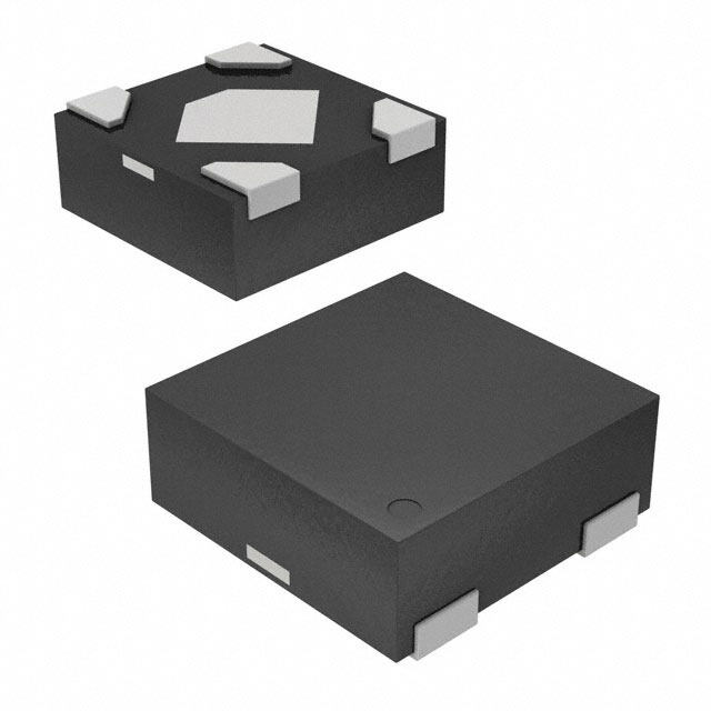
| 产品图片 |
|
| rohs | 符合RoHS无铅 / 符合限制有害物质指令(RoHS)规范要求 |
| 产品系列 | 电源管理 IC,低压差稳压器,Maxim Integrated MAX15027ATB+T- |
| 数据手册 | |
| 产品型号 | MAX15027ATB+T |
| 产品培训模块 | http://www.digikey.cn/PTM/IndividualPTM.page?site=cn&lang=zhs&ptm=25703http://www.digikey.cn/PTM/IndividualPTM.page?site=cn&lang=zhs&ptm=25705 |
| 产品目录页面 | |
| 产品种类 | 低压差稳压器 |
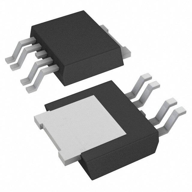
| 供应商器件封装 | 10-TDFN-EP(3x3) |
| 其它名称 | MAX15027ATB+TDKR |
| 包装 | Digi-Reel® |
| 商标 | Maxim Integrated |
| 回动电压—最大值 | 225 mV |
| 安装类型 | 表面贴装 |
| 安装风格 | SMD/SMT |
| 封装 | Reel |
| 封装/外壳 | 10-WFDFN 裸露焊盘 |
| 封装/箱体 | TDFN-EP-10 |
| 工作温度 | -40°C ~ 125°C |
| 工厂包装数量 | 2500 |
| 最大工作温度 | + 125 C |
| 最大输入电压 | 3.6 V |
| 最小工作温度 | - 40 C |
| 最小输入电压 | 1.425 V |
| 标准包装 | 1 |
| 电压-跌落(典型值) | 0.075V @ 1A |
| 电压-输入 | 1.43 V ~ 3.6 V |
| 电压-输出 | 0.5 V ~ 3.3 V |
| 电流-输出 | 1A |
| 电流-限制(最小值) | 1.4A |
| 稳压器拓扑 | 正,可调式 |
| 稳压器数 | 1 |
| 系列 | MAX15027 |
| 线路调整率 | 4 mV |
| 负载调节 | 0.01 mV/mA |
| 输出电压 | 500 mV to 3.3 V |
| 输出电流 | 1 A |
| 输出端数量 | 1 Output |
| 输出类型 | Adjustable |
| 零件号别名 | MAX15027 |


- 商务部:美国ITC正式对集成电路等产品启动337调查
- 曝三星4nm工艺存在良率问题 高通将骁龙8 Gen1或转产台积电
- 太阳诱电将投资9.5亿元在常州建新厂生产MLCC 预计2023年完工
- 英特尔发布欧洲新工厂建设计划 深化IDM 2.0 战略
- 台积电先进制程称霸业界 有大客户加持明年业绩稳了
- 达到5530亿美元!SIA预计今年全球半导体销售额将创下新高
- 英特尔拟将自动驾驶子公司Mobileye上市 估值或超500亿美元
- 三星加码芯片和SET,合并消费电子和移动部门,撤换高东真等 CEO
- 三星电子宣布重大人事变动 还合并消费电子和移动部门
- 海关总署:前11个月进口集成电路产品价值2.52万亿元 增长14.8%


PDF Datasheet 数据手册内容提取
MAX15027/MAX15028 1.425V to 3.6V Input, 1A Low-Dropout Regulators with BIAS Input General Description Features The MAX15027/MAX15028 low-dropout linear regulators ● 1.425V to 3.6V Input Voltage Range operate from input voltages as low as 1.425V and deliver ● Output Voltage Programmable from 0.5V to VIN up to 1A of continuous output current with a typical dropout ● Guaranteed Maximum 225mV Dropout at 1A Output voltage of only 75mV. The output voltage is adjustable Current from 0.5V to VIN and is ±2% accurate over load and line variations, from -40°C to +125°C. The MAX15028 fea- ● ±2% Output Accuracy Over Load, Line, and tures a BIAS input of 3V to 5.5V from an always-on power Temperature supply. The BIAS input current is reduced down to less ● Stable with Ceramic Capacitors than 2µA during shutdown. ● Fast Transient Response These regulators use small, 1µF ceramic input capacitors ● 60µA Operating Bias Supply Current (MAX15028) and 4.7µF ceramic output capacitors to deliver 1A out- put current. High bandwidth provides excellent transient ● 1.2µA Shutdown Bias Supply Current (MAX15028) response and limits the output voltage deviation to 15mV ● Short-Circuit and Thermal Protection for a 500mA load step, with only a 4.7µF ceramic output ● -40°C to +125°C Operating Temperature Range capacitor, and the voltage deviations can be reduced further by increasing the output capacitor. ● Soft-Start Limits Inrush Current These devices offer a logic-controlled shutdown input to ● Thermally Enhanced 3mm x 3mm TDFN Package reduce input current (IIN) consumption down to less than ● AEC-Q100 Qualified 5.5µA in standby mode. Other features include a soft- start to reduce inrush current, short-circuit protection, and thermal-overload protection. The MAX15028 features a BIAS input allowing a secondary supply to keep the LDO’s internal circuitry alive if the voltage on IN goes to 0V. Both devices are fully specified from -40°C to +125°C and are available in a 10-pin thermally enhanced TDFN package (3mm x 3mm) that includes an exposed pad for optimal power dissipation. For a 500mA version of these LDOs, refer to the MAX15029/MAX15030 data sheet. Applications Ordering Information appears at end of data sheet. ● Automotive (Dead-Man LDO) ● Servers ● Storage Typical Operating Circuits and Pin Configurations appear ● Networking at end of data sheet. ● Base Stations ● Optical Modules ● ATE 19-4488; Rev 3; 8/16
MAX15027/MAX15028 1.425V to 3.6V Input, 1A Low-Dropout Regulators with BIAS Input Absolute Maximum Ratings IN, FB, SS, I.C. to GND .......................................-0.3V to +4.0V Operating Junction Temperature Range ..........-40°C to +125°C BIAS to GND ...........................................................-0.3V to +6V Maximum Junction Temperature .....................................+150°C EN to GND ............-0.3V to the lower of (VBIAS + 0.3V) or +6V Storage Temperature Range ............................-65°C to +150°C OUT to GND ..............................................-0.3V to (VIN + 0.3V) Lead Temperature (soldering, 10s) .................................+300°C Output Short-Circuit Duration ....................................Continuous Soldering Temperature (reflow) .......................................+260°C Continuous Power Dissipation (TA = +70°C) 10-Pin TDFN, Multilayer Board (derate 24.4mW/°C above +70°C) ............................1951mW Stresses beyond those listed under “Absolute Maximum Ratings” may cause permanent damage to the device. These are stress ratings only, and functional operation of the device at these or any other conditions beyond those indicated in the operational sections of the specifications is not implied. Exposure to absolute maximum rating conditions for extended periods may affect device reliability. Package Thermal Characteristics (Note 1) Chip Information PROCESS: BiCMOS Junction-to-Ambient Thermal Resistance (θJA) ...............41°C/W Junction-to-Case Thermal Resistance (θJC) ....................9°C/W Note 1: Package thermal resistances were obtained using the method described in JEDEC specification JESD51-7, using a four-layer board. For detailed information on package thermal considerations, refer to www.maximintegrated.com/thermal-tutorial. Package Information For the latest package outline information and land patterns (footprints), go to www.maximintegrated.com/packages. Note that a “+”, “#”, or “-” in the package code indicates RoHS status only. Package drawings may show a different suffix character, but the drawing pertains to the package regardless of RoHS status. PACKAGE TYPE PACKAGE CODE OUTLINE NO. LAND PATTERN NO. 10 TDFN-EP T1033+1 21-0137 90-0003 Electrical Characteristics (Circuit of Figure 1; VIN = 1.8V, VOUT = 1.2V, EN = IN for MAX15027, EN = BIAS for MAX15028, IOUT = 100mA, TA = TJ = -40°C to +125°C. Typical values are at TA = +25°C, unless otherwise noted.) (Note 2) PARAMETER SYMBOL CONDITIONS MIN TYP MAX UNITS IN MAX15027 1.425 3.600 Input Voltage Range VIN VBIAS = 3V to 5.5V 1.425 3.600 V MAX15028 BIAS = IN 3.000 3.600 Undervoltage Lockout VUVLO VIOINU Tr is=i n2gm,A MMAAXX1155002278 11.2.0745 11..312056 11.3.1745 V Undervoltage Lockout Hysteresis VUVLO_HYST 50 mV VIN = 1.425V to 3.6V, VOUT = 1.2V, 160 275 410 IOUT = 1mA, VBIAS = 3.3V Quiescent GND Current IGND µA VIN = 3.6V, VOUT = 3.3V, IOUT = 100mA 180 275 560 VIN = 3.3V, VOUT = 3.3V, IOUT = 500mA 170 315 470 Input Supply Current in Shutdown IIN_SD VEN = 0V, TA = -40°C to +85°C 0.1 5.5 µA www.maximintegrated.com Maxim Integrated │ 2
MAX15027/MAX15028 1.425V to 3.6V Input, 1A Low-Dropout Regulators with BIAS Input Electrical Characteristics (continued) (Circuit of Figure 1; VIN = 1.8V, VOUT = 1.2V, EN = IN for MAX15027, EN = BIAS for MAX15028, IOUT = 100mA, TA = TJ = -40°C to +125°C. Typical values are at TA = +25°C, unless otherwise noted.) (Note 2) PARAMETER SYMBOL CONDITIONS MIN TYP MAX UNITS BIAS (MAX15028) Input Voltage Range VBIAS 3 5.5 V Undervoltage Lockout VBIAS_UVLO VBIAS rising, IOUT = 2mA 2.3 2.5 2.7 V Undervoltage Lockout Hysteresis IOUT = 2mA 110 mV Quiescent Input Supply Current IBIAS VEN = VBIAS 20 60 120 µA VIN = 0V, VOUT = 0V, 1.2 2 VBIAS = 3.3V Input Supply Current in Shutdown IBIAS_SD EN = GND VIN = 3.3V, VOUT = 0V, 1.2 2 µA VBIAS = 3.3V VIN = 3.3V, VOUT = 0V, 1.5 3 VBIAS = 5V OUT Output Voltage Range VOUT 0.5 3.3 V Load Regulation IOUT = 1mA to 1A 0.01 mV/mA Line Regulation VIN = 1.425V to 3.6V, IOUT = 1mA 4 mV Dropout Voltage (VIN - VOUT) VDO IOUT = 1A, VIN = 1.5V 75 225 mV Output Current Limit ILIM VFB = 300mV 1.4 1.7 2.0 A FB Threshold Accuracy VFB V toO U3T.6 =V 0, .I5OVU tTo 3=. 31Vm, VAI Nto = 1(VAOUT + 0.3V) 0.489 0.499 0.509 mV Input Current IFB VFB = 0.688V 0.1 0.2 µA EN/SOFT-START Enable Input Threshold VIH 1.05 (MAX15028) VIL VBIAS = 5V 0.4 V Enable Input Threshold VIH 1.05 (MAX15027) VIL VIN = 1.8V 0.4 V Soft-Start Charging Current ISS 5 µA Soft-Start Reference Voltage VSS 0.499 V THERMAL SHUTDOWN Thermal-Shutdown Threshold TJ rising 165 °C Thermal-Shutdown Hysteresis 15 °C Note 2: All devices are 100% production tested at TA = +25°C. Limits over the operating temperature range are guaranteed by design and characterization. www.maximintegrated.com Maxim Integrated │ 3
MAX15027/MAX15028 1.425V to 3.6V Input, 1A Low-Dropout Regulators with BIAS Input Typical Operating Characteristics (Circuit of Figure 1, VIN = 1.8V, VOUT = 1.5V, IOUT = 1A, TA = +25°C, unless otherwise noted.) MAX15028 MAX15028 INPUT CURRENT (IIN) OUTPUT VOLTAGE vs. INPUT VOLTAGE OUTPUT VOLTAGE vs. OUTPUT CURRENT vs. INPUT VOLTAGE (VIN) 11..46 MAX15027 toc01 11..551250 VBIAS = 3.3V MAX15027 toc02 0.4 MAX15027 toc03 LTAGE (V) 11..02 LTAGE (V)11..550150 RENT (mA) 0.3 VO 0.8 VO1.500 UR 0.2 UT UT T C P 0.6 P1.495 U T T P U U T O O N 0.4 1.490 I 0.1 0.2 IOUT = 0 1.485 VBIAS = 3.3V VBIAS = 3.3V 0 1.480 0 0 0.5 1.0 1.5 2.0 2.5 3.0 3.5 4.0 0 100200 300400500600 7008009001000 0 0.5 1.0 1.5 2.0 2.5 3.0 3.5 4.0 INPUT VOLTAGE (V) OUTPUT CURRENT (mA) INPUT VOLTAGE (V) MAX15028 BIAS CURRENT (IBIAS) MAX15028 BIAS CURRENT (IBIAS) GROUND CURRENT vs. BIAS VOLTAGE (VBIAS) vs. OUTPUT CURRENT vs. OUTPUT CURRENT 5600 MAX15027 toc04 555345 MAX15027 toc05 A)00..3345 MAX15027 toc06 CURRENT (µA) 3400 CURRENT (µA) 555012 VBIAS = 5.5V D CURRENT (m0.33 BIAS 20 BIAS 4489 VBIAS = 3.3V ROUN0.32 G 47 0.31 10 IOUT = 0 46 VBIAS = 3.3V 0 45 0.30 0 1 2 3 4 5 6 0 100 200300 400500 600 700800 9001000 0 0.1 0.2 0.3 0.4 0.5 0.6 0.7 0.8 0.9 1.0 BIAS VOLTAGE (V) OUTPUT CURRENT (mA) LOAD CURRENT (A) MAX15028 DROPOUT VOLTAGE MAX15028 DROPOUT VOLTAGE vs. OUTPUT CURRENT vs. OUTPUT CURRENT V) 112680000 VBIAS = 3.3V MAX15027 toc07 V) 112680000 VBIAS = 3.3V MAX15027 toc07 m m E ( 140 E ( 140 G G A 120 A 120 T T L L VO 100 VO 100 T T OU 80 OU 80 P P RO 60 RO 60 D 40 VIN = 1.4V D 40 VIN = 1.4V 20 20 0 0 0 100 200300 400500 600 700800 9001000 0 100 200300 400500 600 700800 9001000 OUTPUT CURRENT (mA) OUTPUT CURRENT (mA) www.maximintegrated.com Maxim Integrated │ 4
MAX15027/MAX15028 1.425V to 3.6V Input, 1A Low-Dropout Regulators with BIAS Input Typical Operating Characteristics (continued) (Circuit of Figure 1, VIN = 1.8V, VOUT = 1.5V, IOUT = 1A, TA = +25°C, unless otherwise noted.) POWER-UP RESPONSE POWER-DOWN RESPONSE MAX15027 toc09a MAX15027 toc09b VOUT 1V/div VOUT 1V/div VIN 2V/div VIN 2V/div IOUT = 500mA IOUT = 500mA 2ms/div 10µs/div TURN-ON VIA ENABLE RESPONSE TURN-OFF VIA ENABLE RESPONSE MAX15027 toc10a MAX15027 toc10b 1V/div VOUT 1V/div VOUT 2V/div VEN 2V/div VEN IOUT = 500mA IOUT = 500mA 2ms/div 4µs/div www.maximintegrated.com Maxim Integrated │ 5
MAX15027/MAX15028 1.425V to 3.6V Input, 1A Low-Dropout Regulators with BIAS Input Typical Operating Characteristics (continued) (Circuit of Figure 1, VIN = 1.8V, VOUT = 1.5V, IOUT = 1A, TA = +25°C, unless otherwise noted.) POWER-SUPPLY REJECTION RATIO MAX15028 FB VOLTAGE (VFB) vs. FREQUENCY vs. TEMPERATURE 10d5B0/ddiBv MAX15027 toc11 000...555001680 MAX15027 toc12 V) ) (B0.504 VF0.502 E ( AG0.500 T OL0.498 V FB 0.496 0.494 0.492 VBIAS = 3.3V 0.490 100Hz 1MHz -40 -20 0 20 40 60 80 100 120 140 TEMPERATURE (°C) OVERCURRENT THRESHOLD CASE TEMPERATURE RISE vs. TEMPERATURE vs. POWER DISSIPATION ESHOLD (A)1111....77784680 MAX15027 toc13 E RISE (°C) 56780000 MAX15027 toc14 R1.72 R H U T T OVERCURRENT 1111....76660468 CASE TEMPERA 423000 10 1.62 VBIAS = 3.3V 1.60 0 -40 -20 0 20 40 60 80 100 120 140 0 0.5 1.0 1.5 2.0 2.5 TEMPERATURE (°C) POWER DISSIPATION (W) www.maximintegrated.com Maxim Integrated │ 6
MAX15027/MAX15028 1.425V to 3.6V Input, 1A Low-Dropout Regulators with BIAS Input Pin Configurations TOP VIEW TOP VIEW IN 1 + 10 OUT IN 1 + 10 OUT IN 2 9 OUT IN 2 9 OUT IN 3 MAX15027 8 GND BIAS 3 MAX15028 8 GND I.C. 4 7 FB I.C. 4 7 FB EP EP EN 5 6 SS EN 5 6 SS TDFN TDFN (3mm x 3mm) (3mm x 3mm) Pin Description PIN NAME FUNCTION MAX15027 MAX15028 Regulator Input. 1.425V to 3.6V voltage range. Bypass to GND with at least 1µF 1, 2, 3 1, 2 IN of ceramic capacitance. IN is high impedance when the LDO is shut down. Internal Circuitry Supply Input. BIAS supplies the power for the internal circuitry. — 3 BIAS 3V to 5.5V voltage range. 4 4 I.C. Internally Connected. Connect I.C. directly to GND. LDO Enable. Drive EN high to enable the LDO or connect to IN (BIAS for 5 5 EN MAX15028) for always-on operation. Drive EN low to disable the LDO and place the IC in low-power shutdown mode. Soft-Start Input. For typical operation, connect a 0.1µF capacitor from SS to 6 6 SS GND. The soft-start timing is dependent on the value of this capacitor. See the Soft-Start section. Feedback Input. Connect FB to the center of a resistor-divider connected 7 7 FB between OUT and GND to set the output voltage. See the Programming the Output Voltage section. 8 8 GND Ground Regulator Output. Bypass OUT to GND with at least 4.7µF of ceramic 9, 10 9, 10 OUT capacitance for 1A load operation. Exposed Pad. Connect EP to GND and a large copper ground plane to facilitate — — EP package power dissipation. www.maximintegrated.com Maxim Integrated │ 7
MAX15027/MAX15028 1.425V to 3.6V Input, 1A Low-Dropout Regulators with BIAS Input Functional Diagram IN MAX15027 ONLY MAX15028 ONLY REF BIAS MAX15027 MAX15028 IN INTERNAL BIAS UVLO SUPPLY UVLO GENERATOR REF CONTROL LOGIC ERROR AMPLIFIER MOS DRIVER WITH WITH ILIMIT P EN SOFT-START OUT OVERTEMPERATURE PROTECTION SS FB GND www.maximintegrated.com Maxim Integrated │ 8
MAX15027/MAX15028 1.425V to 3.6V Input, 1A Low-Dropout Regulators with BIAS Input Detailed Description 2A. Under these conditions, the device quickly heats up. When the junction temperature reaches +165°C (typ), the The MAX15027/MAX15028 low-dropout linear regulators thermal-overload circuitry turns off the output, allowing the operate from input voltages as low as 1.425V and deliver part to cool down. When the junction temperature cools to up to 1A of continuous output current with a maximum +150°C (typ), the output turns back on and reestablishes dropout voltage of only 225mV. regulation. Current limiting and thermal protection contin- The MAX15028 operates with an input voltage as low ue until the fault is removed. For continuous operation, do as 1.425V if the bias voltage (VBIAS) of 3V to 5.5V is not exceed the absolute maximum junction-temperature available. The power is applied at IN while the control is rating of TJ = +150°C. provided through BIAS input. The current drawn by BIAS is negligible when the LDO goes into shutdown. This feature Soft-Start is especially useful in automotive applications where the The devices feature a soft-start function that slowly ramps BIAS input is derived from an always-on LDO that expects up the output voltage of the regulator based on the value to provide minimal power during the key-off condition. of the capacitor (CSS) connected from SS to GND. Upon The pMOS output stage can be driven from input voltages power-up, CSS is charged with a 5μA (typ) current source down to +1.425V without sacrificing stability or transient through SS. The voltage at SS is compared to the internal performance. The output voltage of all the regulators is 0.5V reference (VREF). The feedback voltage for regula- adjustable from 0.5V to VIN and is ±2% accurate over tion (VREG) is the lower of VSS or VREF. As VSS rises, load and line variations, from -40°C to +125°C. Since the regulation voltage (VREG) rises at the same rate. these regulators have a pMOS output device, supply Once VSS reaches and rises above VREF, the regulation current is not a significant function of load or input head- voltage then tracks the reference voltage since it is the room. lower of VSS and VREF. The value of CSS determines the length of the soft-start time, tSS. Use the following formula Internal p-Channel Pass Transistor to determine CSS. The devices feature a 75mΩ (typ) p-channel MOSFET CSS = 10-5 x tSS pass transistor. Unlike similar designs using pnp pass transistors, p-channel MOSFETs require no base drive, where CSS is in farads and tSS is in seconds. reducing quiescent current. Shutdown Mode pnp-based regulators also waste considerable current in The devices include an enable input. To shut down the dropout when the pass transistor saturates and use high IC, drive EN low. In shutdown mode, the current drawn base-drive currents under large loads. The devices do by BIAS is less than 2μA. This feature is extremely use- not suffer from these problems and consume only 275μA ful in an automotive application where the BIAS input (typ) of quiescent current under heavy loads, as well as is derived from an always-on LDO expecting to provide in dropout. minimal dark current. For normal operation, drive EN high or connect EN to IN (BIAS for MAX15028) for continuous Short-Circuit/Thermal Fault Protection on operation. During shutdown, an internal 10kΩ resistor The devices are fully protected from a short circuit at is connected between OUT and GND. the output through current limiting and thermal-overload circuitry. In the fault condition when the output is shorted to ground, the output current is limited to a maximum of www.maximintegrated.com Maxim Integrated │ 9
MAX15027/MAX15028 1.425V to 3.6V Input, 1A Low-Dropout Regulators with BIAS Input Applications Information Noise, PSRR, and Transient Response The devices are designed to operate with low-dropout Programming the Output Voltage voltages and low quiescent currents while still maintaining The MAX15027/MAX15028 feature an adjustable output good noise performance, transient response, and AC rejec- voltage from 0.5V to VIN using two external resistors con- tion (see the Typical Operating Characteristics for a plot nected as a voltage-divider to FB as shown in Figure 1. of Power-Supply Rejection Ratio (PSRR) vs. Frequency). The output voltage is set by the following equation: When operating from noisy sources, improved supply- noise rejection and transient response can be achieved R1 VOUT =VFB1+ by increasing the values of the input and output bypass R2 capacitors and through passive filtering techniques. The where typically VFB = 0.5V. Choose R2 to be 10kΩ. Or, MAX15027/MAX15028 load-transient response graphs to optimize load-transient response for no load to full load (see the Typical Operating Characteristics) show two transients, use the resistor-divider as a minimum load and components of the output response: a DC shift from the choose R2 to be 500Ω. To simplify resistor selection: output impedance due to the load current change, and the transient response. A typical transient overshoot for a R1=R2VOUT −1 step change in the load current from 300mA to 800mA is VFB 15mV. Use ceramic output capacitors greater than 4.7μF (up to 100μF) to attenuate the overshoot. Capacitor Selection and Regulator Stability Layout Guidelines Capacitors are required at the device’s inputs and outputs The TDFN package has an exposed thermal pad on its for stable operation over the full temperature range and underside. This pad provides a low thermal resistance with load currents up to 1A. Connect a 1μF capacitor path for heat transfer into the PCB. This low thermally between IN and ground and a 4.7μF capacitor with low resistive path carries a majority of the heat away from equivalent series resistance (ESR) between OUT and the IC. The PCB is effectively a heatsink for the IC. The ground for 1A output current. exposed pad should be connected to a large ground The input capacitor (CIN) lowers the source impedance of plane for proper thermal and electrical performance. The the input supply. If input supply source impedance is high, minimum size of the ground plane is dependent upon place a larger input capacitor close to IN to prevent VIN many system variables. To create an efficient path, the sagging due to load transients. Smaller output capacitors exposed pad should be soldered to a thermal landing, can be used for output currents less than 1A. Calculate which is connected to the ground plane by thermal vias. the minimum COUT as follows: The thermal landing should be at least as large as the exposed pad. 1µF COUT =IOUT(MAX)× 0.25A ALWAYS-ON OUTPUT Operating Region and Power Dissipation INPUT 3V BIAS OUT TO 5.5V The maximum power dissipation depends on the thermal INPUT IN R1 resistance of the IC package and circuit board, the tem- 1.2V TO 3.6V perature difference between the die junction and ambi- 1µF ent air, and the rate of airflow. The power dissipated in MAX15028 FB 4.7µF the device is PDISS = IOUT (VIN - VOUT). The package features an exposed thermal pad on its underside. This ENABLE I.C. R2 EN pad lowers the thermal resistance of the package by providing a direct heat conduction path from the die to SHUTDOWN SS GND the PCB. Connect the exposed backside pad and GND to 0.1uF the system ground using a large pad or ground plane and multiple vias to the ground plane layer. Figure 1. MAX15028 Typical Application Circuit www.maximintegrated.com Maxim Integrated │ 10
MAX15027/MAX15028 1.425V to 3.6V Input, 1A Low-Dropout Regulators with BIAS Input Typical Operating Circuits OUTPUT OUTPUT OUT 0.5V TO VIN ALWAYS-ON INPUT BIAS OUT 0.5V TO VIN 3V TO 5.5V INPUT IN INPUT IN 1.425V TO 3.6V 1.425V TO 3.6V 1µF 1µF MAX15027 MAX15028 FB 4.7µF FB 4.7µF EN EN SS GND SS GND Ordering Information PIN- TOP PART TEMP RANGE PACKAGE MARK MAX15027ATB+T -40°C to +125°C 10 TDFN-EP* +AUD MAX15027ATB/V+T -40°C to +125°C 10 TDFN-EP* +AWC MAX15028ATB+T -40°C to +125°C 10 TDFN-EP* +AUE +Denotes a lead(Pb)-free/RoHS-compliant package. T = Tape and reel. *EP = Exposed pad. /V denotes an automotive qualified part. www.maximintegrated.com Maxim Integrated │ 11
MAX15027/MAX15028 1.425V to 3.6V Input, 1A Low-Dropout Regulators with BIAS Input Revision History REVISION REVISION PAGES DESCRIPTION NUMBER DATE CHANGED 0 3/09 Initial release — Revised the Features, Ordering Information, and the Absolute Maximum 1 5/10 1, 2 Ratings. 2 1/15 Changed TOC10a label from 20µs/div to 2ms/div 5 Rebranded data sheet; added new Package Thermal Characteristics section; corrected package code (from T1033-1 to T1033+1) in Package 3 8/16 1, 2, 7, 10, 11 Information table and moved to pg 2; moved Ordering Information table to pg 11, Pin Configuration diagrams to pg 7, and Chip Information table to pg 2 For pricing, delivery, and ordering information, please contact Maxim Direct at 1-888-629-4642, or visit Maxim Integrated’s website at www.maximintegrated.com. Maxim Integrated cannot assume responsibility for use of any circuitry other than circuitry entirely embodied in a Maxim Integrated product. No circuit patent licenses are implied. Maxim Integrated reserves the right to change the circuitry and specifications without notice at any time. The parametric values (min and max limits) shown in the Electrical Characteristics table are guaranteed. Other parametric values quoted in this data sheet are provided for guidance. Maxim Integrated and the Maxim Integrated logo are trademarks of Maxim Integrated Products, Inc. © 2016 Maxim Integrated Products, Inc. │ 12
Mouser Electronics Authorized Distributor Click to View Pricing, Inventory, Delivery & Lifecycle Information: M axim Integrated: MAX15027ATB/V+T MAX15028ATB+T MAX15028ATB/V+T MAX15027ATB+T