ICGOO在线商城 > 集成电路(IC) > 数据采集 - 模数转换器 > MAX1134BEAP+

 Datasheet下载
- 型号: MAX1134BEAP+
- 制造商: Maxim
- 库位|库存: xxxx|xxxx
- 要求:
| 数量阶梯 | 香港交货 | 国内含税 |
| +xxxx | $xxxx | ¥xxxx |
查看当月历史价格
查看今年历史价格
MAX1134BEAP+产品简介:
ICGOO电子元器件商城为您提供MAX1134BEAP+由Maxim设计生产,在icgoo商城现货销售,并且可以通过原厂、代理商等渠道进行代购。 MAX1134BEAP+价格参考。MaximMAX1134BEAP+封装/规格:数据采集 - 模数转换器, 16 Bit Analog to Digital Converter 1 Input 1 SAR 20-SSOP。您可以下载MAX1134BEAP+参考资料、Datasheet数据手册功能说明书,资料中有MAX1134BEAP+ 详细功能的应用电路图电压和使用方法及教程。
MAX1134BEAP+是Maxim Integrated公司生产的一款高速、低功耗的8位模数转换器(ADC),属于数据采集类器件。该芯片采用并行输出接口,具有20MHz的采样速率,适用于对速度和功耗有较高要求的实时信号处理系统。

典型应用场景包括:便携式测试与测量设备,如手持示波器或数据记录仪,得益于其低功耗特性,适合电池供电环境;工业自动化中的传感器信号采集系统,用于将温度、压力、流量等模拟信号快速转换为数字信号供微处理器处理;通信系统中用作中频(IF)信号采样,支持宽带信号的数字化处理;医疗成像设备中的前端数据采集模块,如超声波信号接收处理,要求高采样率和稳定性;此外,也可用于雷达系统、数字示波器、视频处理设备等需要高速数据转换的电子系统。

MAX1134BEAP+工作电压为+5V,采用28引脚DIP封装,便于原型设计和PCB布局,在兼顾性能与可靠性的中高端应用中表现良好。由于其出色的动态性能和抗噪声能力,特别适用于模拟信号变化较快且环境干扰较强的场合。总之,MAX1134BEAP+是一款适用于高速、低功耗模拟信号数字化需求的通用型ADC,广泛应用于工业、通信、医疗及测试测量等领域。
| 参数 | 数值 |
| 产品目录 | 集成电路 (IC)半导体 |
| 描述 | IC ADC 16BIT 150KSPS 20-SSOP模数转换器 - ADC 16-Bit 150ksps 3.3V Single Supply |
| 产品分类 | |
| 品牌 | Maxim Integrated |
| 产品手册 | |
| 产品图片 |
|
| rohs | 符合RoHS无铅 / 符合限制有害物质指令(RoHS)规范要求 |
| 产品系列 | 数据转换器IC,模数转换器 - ADC,Maxim Integrated MAX1134BEAP+- |
| 数据手册 | |
| 产品型号 | MAX1134BEAP+ |
| 产品培训模块 | http://www.digikey.cn/PTM/IndividualPTM.page?site=cn&lang=zhs&ptm=25703http://www.digikey.cn/PTM/IndividualPTM.page?site=cn&lang=zhs&ptm=25705 |
| 产品目录页面 | |
| 产品种类 | 模数转换器 - ADC |
| 位数 | 16 |
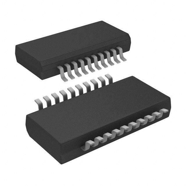
| 供应商器件封装 | 20-SSOP |
| 信噪比 | 84 dB |
| 分辨率 | 16 bit |
| 包装 | 管件 |
| 商标 | Maxim Integrated |
| 安装类型 | 表面贴装 |
| 安装风格 | SMD/SMT |
| 封装 | Tube |
| 封装/外壳 | 20-SSOP(0.209",5.30mm 宽) |
| 封装/箱体 | SSOP-20 |
| 工作温度 | -40°C ~ 85°C |
| 工作电源电压 | 3.135 V to 3.465 V |
| 工厂包装数量 | 66 |
| 应用说明 | |
| 接口类型 | QSPI, SPI, Serial (3-Wire, Microwire) |
| 数据接口 | MICROWIRE™,QSPI™,串行,SPI™ |
| 最大功率耗散 | 640 mW |
| 最大工作温度 | + 85 C |
| 最小工作温度 | - 40 C |
| 标准包装 | 1 |
| 特性 | PGA |
| 电压参考 | 2.048 V |
| 电压源 | 模拟和数字 |
| 系列 | MAX1134B |
| 结构 | SAR |
| 转换器数 | 1 |
| 转换器数量 | 1 |
| 转换速率 | 150 kS/s |
| 输入数和类型 | 1 个单端,单极1 个单端,双极 |
| 输入类型 | Single-Ended |
| 通道数量 | 1 Channel |
| 采样率(每秒) | 150k |
| 零件号别名 | MAX1134B |


- 商务部:美国ITC正式对集成电路等产品启动337调查
- 曝三星4nm工艺存在良率问题 高通将骁龙8 Gen1或转产台积电
- 太阳诱电将投资9.5亿元在常州建新厂生产MLCC 预计2023年完工
- 英特尔发布欧洲新工厂建设计划 深化IDM 2.0 战略
- 台积电先进制程称霸业界 有大客户加持明年业绩稳了
- 达到5530亿美元!SIA预计今年全球半导体销售额将创下新高
- 英特尔拟将自动驾驶子公司Mobileye上市 估值或超500亿美元
- 三星加码芯片和SET,合并消费电子和移动部门,撤换高东真等 CEO
- 三星电子宣布重大人事变动 还合并消费电子和移动部门
- 海关总署:前11个月进口集成电路产品价值2.52万亿元 增长14.8%


PDF Datasheet 数据手册内容提取
19-2464; Rev 0; 4/02 16-Bit ADCs, 150ksps, 3.3V Single Supply General Description Features M The MAX1134/MAX1135 are 150ksps, 16-bit ADCs. (cid:2) 150ksps (Bipolar) and 125ksps (Unipolar) A These serially interfaced ADCs connect directly to SPI™, Sampling ADC X QSPI™, and MICROWIRE™ devices without external (cid:2) 16 Bits, No Missing Codes logic. They combine an input scaling network, internal 1 track/hold (T/H), clock, and three general-purpose digital (cid:2) 1LSB INL (typ) Guaranteed 1 output pins (for external multiplexer or PGA control) in a (cid:2) -100dB THD 3 20-pin SSOP package. The excellent dynamic perfor- (cid:2) 3.3V Single-Supply Operation mance (THD ≥ 90dB), high speed (150ksps in bipolar 4 mode), and low power (8.0mA) of these ADCs make (cid:2) Low-Power Operation / M them ideal for applications such as industrial process 4.5mA (typ) (Unipolar Mode) control, instrumentation, and medical applications. (cid:2) 1.2µA Shutdown Mode A The MAX1134 accepts input signals of 0 to +6V (unipo- (cid:2) Software-Configurable Unipolar and Bipolar Input X lar) or ±6V (bipolar), while the MAX1135 accepts input Ranges 1 signals of 0 to +2.048V (unipolar) or ±2.048V (bipolar). 0 to +6V and ±6V (MAX1134) 1 Operating from a single 3.135V to 3.465V analog and 0 to +2.048V and ±2.048V (MAX1135) digital supply, power-down modes reduce current con- (cid:2) Internal or External Clock 3 sumption to 0.15mA at 10ksps and further reduce sup- 5 (cid:2) SPI/QSPI/MICROWIRE TMS320-Compatible Serial ply current to less than 20µA at slower data rates. Interface A serial strobe output (SSTRB) allows direct connection (cid:2) Three User-Programmable Logic Outputs to the TMS320 family digital-signal processors. The MAX1134/MAX1135 user can select either the internal (cid:2) Small 20-Pin SSOP Package clock or an external serial-interface clock for the ADC to perform analog-to-digital conversions. Ordering Information The MAX1134/MAX1135 feature internal calibration cir- cuitry to correct linearity and offset errors. On-demand TEMP PIN- INL calibration allows the user to optimize performance. PART RANGE PACKAGE (LSB) Three user-programmable logic outputs are provided MAX1134BCAP 0°C to +70°C 20 SSOP ±2.5 for the control of an 8-channel mux or PGA. MAX1134BEAP -40°C to +85°C 20 SSOP ±2.5 The MAX1134/MAX1135 are available in a 20-pin SSOP package and are fully specified over the -40°C to Ordering Information continued at end of data sheet. +85°C temperature range. Applications Pin Configuration Industrial Process Control TOP VIEW Industrial I/O Modules Data-Acquisition Systems REF 1 20 AIN Medical Instruments AVDD 2 19 AGND AGND 3 18 CREF Portable and Battery-Powered Equipment AVDD 4 17 CS DGND 5 MAX1134 16 DIN MAX1135 Functional Diagram and Typical Application Circuit appear SHDN 6 15 DVDD at end of data sheet. P2 7 14 DGND P1 8 13 SCLK PO 9 12 RST SPI and QSPI are trademarks of Motorola, Inc. SSTRB 10 11 DOUT MICROWIRE is a trademark of National Semiconductor, Corp. SSOP ________________________________________________________________Maxim Integrated Products 1 For pricing, delivery, and ordering information,please contact Maxim/Dallas Direct!at 1-888-629-4642, or visit Maxim’s website at www.maxim-ic.com.
16-Bit ADCs, 150ksps, 3.3V Single Supply 5 ABSOLUTE MAXIMUM RATINGS 3 AVDDto AGND, DVDDto DGND..............................-0.3V to +6V Operating Temperature Ranges 1 AGND to DGND.....................................................-0.3V to +0.3V MAX113_ _CAP...................................................0°C to +70°C AIN to AGND ....................................................................±16.5V MAX113_ _EAP................................................-40°C to +85°C 1 CREF, REF to AGND................................-0.3V to (AVDD+ 0.3V) Storage Temperature Range.............................-60°C to +150°C X Digital Inputs to DGND.............................................-0.3V to +6V Junction Temperature......................................................+150°C A Digital Outputs to DGND.........................-0.3V to (DVDD+ 0.3V) Lead Temperature (soldering, 10s).................................+300°C Continuous Power Dissipation (TA= +70°C) M 20-Pin SSOP (derate 8.00mW/°C above +70°C).........640mW / 4 Stresses beyond those listed under “Absolute Maximum Ratings” may cause permanent damage to the device. These are stress ratings only, and functional 3 operation of the device at these or any other conditions beyond those indicated in the operational sections of the specifications is not implied. Exposure to absolute maximum rating conditions for extended periods may affect device reliability. 1 1 ELECTRICAL CHARACTERISTICS X (AVDD= DVDD= 3.3V ±5%, fSCLK= 3.6MHz, external clock (50% duty cycle), 24 clocks/conversion (150ksps), bipolar input, VREF= A 2.048V, CREF= 4.7µF, CCREF= 1µF, TA= TMINto TMAX, unless otherwise noted. Typical values are at TA= +25°C.) M PARAMETER SYMBOL CONDITIONS MIN TYP MAX UNITS DC ACCURACY (Note 1) Resolution 16 Bits Relative Accuracy INL Bipolar mode (Note 2) MAX113_B 1.0 ±2.5 LSB No Missing Codes 16 Bits Differential Nonlinearity DNL Bipolar mode MAX113_B -1 +1.75 LSB Transition Noise 1.5 LSBRMS Unipolar ±4 Offset Error mV Bipolar ±6 Unipolar ±0.2 Gain Error (Note 3) %FSR Bipolar ±0.3 Offset Drift (Bipolar and Unipolar) Excluding reference drift ±1 ppm/°C Gain Drift (Bipolar and Unipolar) Excluding reference drift ±4 ppm/°C DY NAM I C SPECI FI CA T I ON S (5 k H z SINE-WAVE INPUT, 150 k s p s, 3. 6MH z CLOCK, BIPOLAR INPUT MODE. MA X 11 34 , 12 V P-P. MA X 11 3 5 , 4. 09 6 V P-P.) Signal-to-Noise Plus Distortion fIN = 5kHz 80 84 dB (SINAD) fIN = 75kHz 83 fIN = 5kHz 80 84 Signal-to-Noise Ratio (SNR) dB fIN = 75kHz 83 fIN = 5kHz -100 -90 Total Harmonic Distortion (THD) dB fIN = 75kHz -93 Spurious-Free Dynamic Range fIN = 5kHz 92 105 dB (SFDR) fIN = 75kHz 97 ANALOG INPUT Unipolar 0 +6 MAX1134 Bipolar -6 +6 Input Range V Unipolar 0 +2.048 MAX1135 Bipolar -2.048 +2.048 2 _______________________________________________________________________________________
16-Bit ADCs, 150ksps, 3.3V Single Supply ELECTRICAL CHARACTERISTICS (continued) M (AVDD= DVDD= 3.3V ±5%, fSCLK= 3.6MHz, external clock (50% duty cycle), 24 clocks/conversion (150ksps), bipolar input, VREF= A 2.048V, CREF= 4.7µF, CCREF= 1µF, TA= TMINto TMAX, unless otherwise noted. Typical values are at TA= +25°C.) X PARAMETER SYMBOL CONDITIONS MIN TYP MAX UNITS 1 Unipolar 7.5 10.5 MAX1134 1 Bipolar 5.9 8.4 Input Impedance kΩ 3 Unipolar 100 1000 MAX1135 4 Bipolar 3.4 5.3 / Input Capacitance 32 pF M CONVERSION RATE A Internal Clock Frequency 3 MHz X Aperture Delay tAD 10 ns 1 Aperture Jitter tAJ 50 ps 1 MODE 1 (24 EXTERNAL CLOCK CYCLES PER CONVERSION) 3 Unipolar 0.1 3.0 5 External Clock Frequency fSCLK MHz Bipolar 0.1 3.6 fS = Unipolar 4.17 125 Sample Rate ksps fSCLK / 24 Bipolar 4.17 150 tCONV+ACQ Unipolar 8 240 Conversion Time (Note 4) = 24 / µs fSCLK Bipolar 6.7 240 MODE 2 (INTERNAL CLOCK MODE) External Clock Frequency 4 MHz (Data Transfer Only) Conversion Time (SSTRB low pulse width) 5.3 7 µs Unipolar 1.67 Acquisition Time (Note 5) µs Bipolar 1.39 MODE 3 (32 EXTERNAL CLOCK CYCLES PER CONVERSION) External Clock Frequency fSCLK Unipolar or bipolar 0.1 3.6 MHz fS = Sample Rate Unipolar or bipolar 3.125 112 ksps fSCLK / 32 tCONV+ACQ Conversion Time (Note 4) = 32 / Unipolar or bipolar 8.89 320 µs fSCLK EXTERNAL REFERENCE Input Range (Notes 6, 7) 1.9 2.048 2.2 V VREF = 2.048V, fSCLK = 3.6MHz 110 Input Current VREF = 2.048V, fSCLK = 0 100 µA In power-down, fSCLK = 0 0.1 DIGITAL INPUTS Input High Voltage VIH 2.4 V Input Low Voltage VIL 0.8 V Input Leakage IIN VIN = 0 or DVDD -1 +1 µA _______________________________________________________________________________________ 3
16-Bit ADCs, 150ksps, 3.3V Single Supply 5 ELECTRICAL CHARACTERISTICS (continued) 3 (AVDD= DVDD= 3.3V ±5%, fSCLK= 3.6MHz, external clock (50% duty cycle), 24 clocks/conversion (150ksps), bipolar input, VREF= 1 2.048V, CREF= 4.7µF, CCREF= 1µF, TA= TMINto TMAX, unless otherwise noted. Typical values are at TA= +25°C.) 1 PARAMETER SYMBOL CONDITIONS MIN TYP MAX UNITS X Input Hysteresis VHYST 0.2 V A Input Capacitance CIN 10 pF M DIGITAL OUTPUTS 4/ Output High Voltage VOH ISOURCE = 0.5mA DV0D.5D - V 3 ISINK = 5mA 0.4 1 Output Low Voltage VOL V ISINK = 16mA 0.8 1 Three-State Leakage Current IL CS = DVDD -10 +10 µA X Three-State Output Capacitance CS = DVDD 10 pF A POWER SUPPLIES M Analog Supply AVDD 3.135 3.3 3.465 V Digital Supply DVDD 3.135 3.3 3.465 V Unipolar mode 3.9 8 mA Analog Supply Current IANALOG Bipolar mode 7 11 SHDN = 0, or software power-down mode 0.1 10 µA Unipolar or bipolar mode 1 2 mA Digital Supply Current IDIGITAL SHDN = 0, or software power-down mode 1.1 10 µA Power-Supply Rejection Ratio PSRR AVDD = DVDD = 3.135V to 3.465V 65 dB (Note 8) TIMING CHARACTERISTICS (Figures 5 and 6) (AVDD= DVDD= 3.3V ±5%, TA= TMINto TMAX, unless otherwise noted.) PARAMETER SYMBOL CONDITIONS MIN TYP MAX UNITS DIN to SCLK Setup tDS 50 ns DIN to SCLK Hold tDH 0 ns SCLK to DOUT Valid tDO 70 ns CS Fall to DOUT Enable tDV CLOAD = 50pF 80 ns CS Rise to DOUT Disable tTR CLOAD = 50pF 80 ns CS to SCLK Rise Setup tCSS 100 ns CS to SCLK Rise Hold tCSH 0 ns SCLK High Pulse Width tCH 120 ns SCLK Low Pulse Width tCL 120 ns SCLK Fall to SSTRB tSSTRB CLOAD = 50pF 80 ns CS Fall to SSTRB Enable tSDV CLOAD = 50pF, external clock mode 80 ns CS Rise to SSTRB Disable tSTR CLOAD = 50pF, external clock mode 80 ns SSTRB Rise to SCLK Rise tSCK Internal clock mode 0 ns RST Pulse Width tRS 278 70 ns 4 _______________________________________________________________________________________
16-Bit ADCs, 150ksps, 3.3V Single Supply TIMING CHARACTERISTICS (Figures 5 and 6) (continued) M (AVDD= DVDD= 3.3V ±5%, TA= TMINto TMAX, unless otherwise noted.) A Note 1: Tested at AVDD= DVDD = 3.3V, bipolar input mode. X Note 2: Relative accuracy is the deviation of the analog value at any code from its theoretical value after the gain error and offset 1 error have been nullified. 1 Note 3: Offset nullified. Note 4: Conversion time is defined as the number of clock cycles multiplied by the clock period; clock has 50% duty cycle. Includes 3 the acquisition time. 4 Note 5: Acquisition time is 5 clock cycles in short acquisition mode and 13 clock cycles in long acquisition mode. / Note 6: Performance is limited by the converter’s noise floor, typically 300µVP-P. M Note 7: When an external reference has a different voltage than the specified typical value, the full scale of the ADC scales propor- A tionally. Note 8: Defined as the change in positive full scale caused by a ±5% variation in the nominal supply voltage. X 1 1 3 Typical Operating Characteristics 5 (MAX1134/MAX1135, AVDD = DVDD = 3.3V, fSCLK = 3.6MHz, external clock (50% duty cycle), 24 clocks/conversion (150ksps), bipolar input, REF = 2.048V, 4.7µF on REF, 1µF on CREF, TA= +25°C, unless otherwise noted.) INTEGRAL NONLINEARITY DIFFERENTIAL NONLINEARITY TOTAL SUPPLY CURRENT vs. DIGITAL OUTPUT CODE vs. DIGITAL OUTPUT CODE vs. TEMPERATURE NTEGRAL NONLINEARITY (LSB) -01123 MAX1134/35 toc01 FFERENTIAL NONLINEARITY (LSB) ---00000001........248606240 MX1134/35 toc02 TOTAL SUPPLY CURRENT (mA) 888888889.........234567890 ABC::: AAAVVVDDDDDD,,, DDDVVVDDDDDD === 333...1343V655VVCBA MAX1134/35 toc03 I -2 DI -0.8 8.1 -3 -1.0 8.0 1 13273 26545 39817 53089 59725 1 13649 27297 40945 54593 61417 -40 -20 0 20 40 60 80 DIGITAL OUTPUT CODE DIGITAL OUTPUT CODE TEMPERATURE (°C) _______________________________________________________________________________________ 5
16-Bit ADCs, 150ksps, 3.3V Single Supply 5 Typical Operating Characteristics (continued) 3 (MAX1134/MAX1135, AVDD = DVDD = 3.3V, fSCLK = 3.6MHz, external clock (50% duty cycle), 24 clocks/conversion (150ksps), 1 bipolar input, REF = 2.048V, 4.7µF on REF, 1µF on CREF, TA= +25°C, unless otherwise noted.) 1 OFFSET VOLTAGE GAIN ERROR TOTAL SUPPLY CURRENT vs. X vs. TEMPERATURE vs. TEMPERATURE CONVERSION RATE (USING SHUTDOWN) A -0.5 0.06 100 X1134/M OFFSET ERROR (mV) ---211...050 ABC::: AAAVVVDDDDDD,,, DDDVVVDDDDDD === 333...134C3V655VV A MAX1134/35 toc04 N ERROR (% FULL SCALE) 0000....00003245 BA C MAX1134/35 toc05 AL SUPPLY CURRENT (mA) 101 MAX1134/35 toc06 A -2.5 GAI 0.01 A: AVDD, DVDD = 3.135V TOT 0.1 B B: AVDD, DVDD = 3.3V M C: AVDD, DVDD = 3.465V -3.0 0 0.01 -40 -20 0 20 40 60 80 -40 -20 0 20 40 60 80 0 1 10 100 1000 TEMPERATURE (°C) TEMPERATURE (°C) CONVERSION RATE (ksps) FFT PLOT SINAD PLOT 0 100 -20 ffSINA M= P5LkEH =z 150kHz MAX1134/35 toc07 8900 fSAMPLE = 150kHz MAX1134/35 toc08 70 B) -40 B) DE (d DE (d 60 MPLITU -60 MPLITU 4500 A -80 A 30 20 -100 10 -120 0 0 10 20 30 40 50 60 70 0.1 1 10 100 FREQUENCY (kHz) FREQUENCY (kHz) SFDR PLOT THD PLOT 120 0 11019000 fSAMPLE = 150kHz MAX1134/35 toc09 ---321000 fSAMPLE = 150kHz MAX1134/35 toc10 dB) 80 dB) -40 DE ( 70 DE ( -50 PLITU 5600 PLITU -60 M M A 40 A -70 30 -80 20 -90 10 -100 0 -110 0.1 1 10 100 0.1 1 10 100 FREQUENCY (kHz) FREQUENCY (kHz) 6 _______________________________________________________________________________________
16-Bit ADCs, 150ksps, 3.3V Single Supply Pin Description M PIN NAME FUNCTION A 1 REF ADC Reference Input. Connect a 2.048V voltage source to REF. Bypass REF to AGND with a 4.7µF capacitor. X 2 AVDD Analog Supply. Connect to pin 4. 1 1 3 AGND Analog Ground. This is the primary analog ground (star ground). 3 4 AVDD Analog Supply, 3.3V ±5%. Bypass AVDD to AGND (pin 3) with a 0.1µF capacitor. 4 5 DGND Digital Ground /M 6 SHDN Shutdown Control Input. Drive SHDN low to put the ADC in shutdown mode. A 7 P2 User-Programmable Output 2 X 8 P1 User-Programmable Output 1 1 1 9 P0 User-Programmable Output 0 3 Serial Strobe Output. In internal clock mode, SSTRB goes low when the ADC begins a conversion and goes 5 10 SSTRB high when the conversion is finished. In external clock mode, SSTRB pulses high for one clock period before the MSB decision. It is high impedance when CS is high in external clock mode. Serial Data Output. MSB first, straight binary format for unipolar input, two’s complement for bipolar input. 11 DOUT Each bit is clocked out of DOUT at the falling edge of SCLK. 12 RST Reset Input. Drive RST low to put the device in the power-on default mode. See the Power-On Reset section. Serial Data Clock Input. Serial data on DIN is loaded on the rising edge of SCLK, and serial data is updated 13 SCLK on DOUT on the falling edge of SCLK. In external clock mode, SCLK sets the conversion speed. 14 DGND Digital Ground. Connect to pin 5. 15 DVDD Digital Supply, 3.3V ±5%. Bypass DVDD to DGND (pin 14) with a 0.1µF capacitor. 16 DIN Serial Data Input. Serial data on DIN is latched on the rising edge of SCLK. Chip-Select Input. Drive CS low to enable the serial interface. When CS is high, DOUT is high impedance. In 17 CS external clock mode, SSTRB is high impedance when CS is high. 18 CREF Reference Buffer Bypass. Bypass CREF to AGND (pin 3) with a 1µF capacitor. 19 AGND Analog Ground. Connect to pin 3. 20 AIN Analog Input _______________________________________________________________________________________ 7
16-Bit ADCs, 150ksps, 3.3V Single Supply 5 Detailed Description In addition to a 16-bit ADC, the MAX1134/MAX1135 include an input scaler, an internal digital microcontroller, 3 The MAX1134/MAX1135 ADCs use a successive- calibration circuitry, and an internal clock generator. 1 approximation technique and input track/hold (T/H) cir- 1 cuitry to convert an analog signal to a 16-bit digital The input scaler for the MAX1134 enables conversion output. The MAX1134/MAX1135 easily interface to of input signals ranging from 0 to +6V (unipolar input) X microprocessors (µPs). The data bits can be read either or ±6V (bipolar input). The MAX1135 accepts 0 to A during the conversion in external clock mode or after the +2.048V (unipolar input) or ±2.048V (bipolar input). The M conversion in internal clock mode. input range is software selectable. Calibration / 4 To minimize linearity, offset, and gain errors, the 3 MAX1134/MAX1135 have on-demand software calibra- tion. Initiate calibration by writing a control byte with bit 1 M1 = 0 and bit M0 = 1 (Table 1). Select internal or exter- 1 S1 BIPOLAR VOLTAGE nal clock for calibration by setting the INT/EXT bit in the X REFERENCE control byte. Calibrate the MAX1134/MAX1135 with the A 2.5kRΩ1 UNIPOLAR same clock mode used for performing conversions. M R2 TRACK C3H2OpLFD Offsets resulting from synchronous noise (such as the AIN S2 conversion clock) are canceled by the MAX1134/ T/H OUT MAX1135’s calibration circuitry. However, because the R3 HOLD TRACK HOLD magnitude of the offset produced by a synchronous S3 signal depends on the signal’s shape, recalibration may be appropriate if the shape or relative timing of the clock, or other digital signals change, as may occur if more than one clock signal or frequency is used. S1 = BIPOLAR/UNIPOLAR R2 = 7.6kΩ (MAX1134) S2, S3 = T/H SWITCH OR 2.5kΩ (MAX1135) Input Scaler R3 = 3.9kΩ (MAX1134) OR INFINITY (MAX1135) The MAX1134/MAX1135 have an input scaler, which allows conversion of true bipolar input voltages while operating from a single 3.3V supply. The input scaler attenuates and shifts the input as necessary to map the external input range to the input range of the internal Figure 1. Equivalent Input Circuit ADC. The MAX1134 analog input range is 0 to +6V (unipolar) or ±6V (bipolar). The MAX1135 analog input Table 1. Control Byte Format BIT NAME DESCRIPTION 7 (MSB) START The first logic 1 bit after CS goes low defines the beginning of the control byte. 1 = unipolar, 0 = bipolar. Selects unipolar or bipolar conversion mode. In unipolar mode, analog input 6 UNI/BIP signals from 0 to +6V (MAX1134) or 0 to +VREF (MAX1135) can be converted. In bipolar mode, analog input signals from -6V to +6V (MAX1134) or -VREF to +VREF (MAX1135) can be converted. 5 INT/EXT Selects the internal or external conversion clock. 1 = internal, 0 = external. M1 M0 Mode 4 M1 0 0 24 external clocks per conversion (short acquisition mode) 0 1 Start calibration: starts internal calibration 1 0 Software power-down mode 3 M0 1 1 32 external clocks per conversion (long acquisition mode) 2 P2 These 3 bits are stored in a port register and output to pins P2, P1, and P0 for use in addressing a mux 1 P1 or PGA. These 3 bits are updated in the port register simultaneously when a new control byte is written. 0 (LSB) P0 8 _______________________________________________________________________________________
16-Bit ADCs, 150ksps, 3.3V Single Supply M CS A tACQ X 1 4 8 12 15 21 24 SCLK 1 UNI/ INT/ 1 START M1 M0 P2 P1 P0 DIN BIP EXT 3 SSTRB 4 / M B15 B0 FILLED WITH DOUT MSB B14 B13 B12 B11 B10 B9 B4 B3 B2 B1 LSB ZEROS A A/D IDLE ACQUISITION CONVERSION IDLE X STATE 1 Figure 2. Short Acquisition Mode (24 Clock Cycles) External Clock 1 3 Table 2. User-Programmable Outputs 5 PROGRAMMED POWER-ON OR OUTPUT PIN THROUGH CONTROL DESCRIPTION RST DEFAULT BYTE P2 Bit 2 0 User-programmable outputs follow the state of the control byte’s 3 LSBs, and are updated simultaneously when a new P1 Bit 1 0 control byte is written. Outputs are push-pull. In hardware and software shutdown, these outputs are unchanged and remain P0 Bit 0 0 low impedance. range is 0 to +2.048V (unipolar) or ±2.048V (bipolar). low or after a conversion or calibration completes, the Unipolar and bipolar mode selection is configured with first logic 1 clocked into DIN is interpreted as the bit 6 of the serial control byte (Table 1). START bit, the MSB of the 8-bit control byte. Figure 1 shows the equivalent input circuit of the The SCLK input is the serial-data-transfer clock, which MAX1134/MAX1135. The resistor network on the analog clocks data in and out of the MAX1134/MAX1135. input provides ±16.5V fault protection. This circuit limits SCLK also drives the ADC conversion steps in external the current going into or out of the pin to less than 2mA. clock mode (see the Internal and External Clock Modes The overvoltage protection is active even if the device section). is in a power-down mode, or if AVDD= 0. DOUT is the serial output of the conversion result. Digital Interface DOUT is updated on the falling edge of SCLK. DOUT is The digital interface pins consist of SHDN, RST, high impedance when CSis high. SSTRB, DOUT, SCLK, DIN, and CS. Bringing SHDNlow CSmust be low for the MAX1134/MAX1135 to accept a places the MAX1134/MAX1135 in its 1.2µA shutdown control byte. The serial interface is disabled when CSis mode. A logic low on RSThalts the MAX1134/MAX1135 high. operation and returns the part to its power-on-reset User-Programmable Outputs state. The MAX1134/MAX1135 have three user-program- In external clock mode, SSTRB is low and pulses high mable outputs: P0, P1, and P2. The power-on default for one clock cycle at the start of conversion. In internal state for the programmable outputs is zero. These are clock mode, SSTRB goes low at the start of the conver- push-pull CMOS outputs suitable for driving a multi- sion, and goes high to indicate that the conversion is plexer, a PGA, or other signal preconditioning circuitry. finished. Bits 0, 1, and 2 of the control byte control the user-pro- The DIN input accepts control byte data, which is grammable outputs (Tables 1, 2). clocked in on each rising edge of SCLK. After CS goes _______________________________________________________________________________________ 9
16-Bit ADCs, 150ksps, 3.3V Single Supply 5 CS 3 1 tACQ 1 1 4 8 14 15 29 32 X SCLK A DIN START UBNIPI/ IENXTT/ M1 M0 P2 P1 P0 M SSTRB / 4 B15 B0 FILLED WITH 3 DOUT MSB B14 B13 B4 B3 B2 B1 LSB ZEROS 1 A/D IDLE ACQUISITION CONVERSION IDLE 1 STATE X Figure 3. Long Acquisition Mode (32 Clock Cycles) External Clock A M CS tSDV tSTR SSTRB tSSTRB tSSTRB SCLK P1 CLOCKED IN Figure 4. External Clock Mode SSTRB Detailed Timing The user-programmable outputs are set to zero during Internal and External Clock Modes power-on reset or when RSTgoes low. During hardware The MAX1134/MAX1135 use either the external serial or software shutdown, P0, P1, and P2 are unchanged clock or the internal clock to perform the successive- and remain low impedance. approximation conversion. In both clock modes, the external clock shifts data in and out of the Starting a Conversion MAX1134/MAX1135. Bit 5 (INT/EXT) of the control byte Start a conversion by clocking a control byte into the programs the clock mode. device’s internal shift register. With CS low, each rising edge on SCLK clocks a bit from DIN into the External Clock MAX1134/MAX1135s’ internal shift register. After CS In external clock mode, the external clock not only goes low or after a conversion or calibration completes, shifts data in and out, but also drives the ADC conver- the first arriving logic 1 is defined as the start bit of the sion steps. control byte. Until this first start bit arrives, any number of In short acquisition mode, SSTRB pulses high for one logic 0 bits can be clocked into DIN with no effect. If at clock period after the seventh falling edge of SCLK fol- any time during acquisition or conversion CS is brought lowing the start bit. The MSB of the conversion is avail- high and then low again, the part is placed into a state able at DOUT on the eighth falling edge of SCLK where it can recognize a new start bit. If a new start bit (Figure 2). occurs before the current conversion is complete, the conversion is aborted and a new acquisition is initiated. 10 ______________________________________________________________________________________
16-Bit ADCs, 150ksps, 3.3V Single Supply M CS A X tACQ 1 1 4 8 9 10 21 24 SCLK 1 UNI/ INT/ 3 DIN START BIP EXT M1 M0 P2 P1 P0 4 / SSTRB M tCONV A B15 B0 FILLED WITH DOUT MSB B14 B13 B4 B3 B2 B1 LSB ZEROS X 1 1 Figure 5. Internal Clock Mode Timing, Short Acquisition 3 5 CS tCONV tCSS tCSH tSCK SSTRB tSSTRB SCLK P0 CLOCKED IN NOTE: FOR BEST NOISE PERFORMANCE, KEEP SCLK LOW DURING CONVERSION. Figure 6. Internal Clock Mode SSTRB Detailed Timing In long acquisition mode, when using external clock, SSTRB goes low at the start of the conversion and goes SSTRB pulses high for one clock period after the 15th high when the conversion is complete. SSTRB is low for falling edge of SCLK following the start bit. The MSB of a maximum of 7µs, during which time SCLK should the conversion is available at DOUT on the 16th falling remain low for best noise performance. An internal reg- edge of SCLK (Figure 3). ister stores data when the conversion is in progress. SCLK clocks the data out of the internal storage regis- In external clock mode, SSTRB is high impedance when ter at any time after the conversion is complete. CSis high (Figure 4). CSis normally held low during the entire conversion. If CS goes high during the conver- The MSB of the conversion is available at DOUT when sion, SCLK is ignored until CS goes low. This allows SSTRB goes high. The subsequent 15 falling edges on external clock mode to be used with 8-bit bytes. SCLK shift the remaining bits out of the internal storage register (Figure 5). CS does not need to be held low Internal Clock once a conversion is started. In internal clock mode, the MAX1134/MAX1135 gener- ate their own conversion clock. This frees the micro- When internal clock mode is selected, SSTRB does not processor from the burden of running the SAR go into a high-impedance state when CS goes high. conversion clock, and allows the conversion results to Figure 6 shows the SSTRB timing in internal clock be read back at the processor’s convenience, at any mode. In internal clock mode, data can be shifted into clock rate up to 4MHz. the MAX1134/MAX1135 at clock rates up to 4MHz, pro- ______________________________________________________________________________________ 11
16-Bit ADCs, 150ksps, 3.3V Single Supply 5 Table 3. Unipolar Full Scale and Zero Table 4. Bipolar Full Scale, Zero Scale, 3 Scale and Negative Full Scale 1 PART ZERO SCALE FULL SCALE NEGATIVE FULL ZERO 1 PART FULL SCALE MAX1134 0 +6 (VREF/2.048) SCALE SCALE X MAX1135 0 +VREF MAX1134 -6 (VREF/2.048) 0 +6 (VREF/2.048) A MAX1135 -VREF 0 +VREF M vided the minimum acquisition time, tACQ, is kept power supplies and the reference voltage have fully / above 1.39µs in bipolar mode and 1.67µs in unipolar settled prior to initiating the calibration sequence. 4 mode. Data can be clocked out at 4MHz. 3 Initiate calibration by setting M1 = 0 and M0 = 1 in the Output Data control byte. In internal clock mode, SSTRB goes low at 1 The output data format is straight binary for unipolar the beginning of calibration and goes high to signal the 1 conversions and two’s complement in bipolar mode. end of calibration, approximately 80,000 clock cycles X The MSB is shifted out of the MAX1134/MAX1135 first later. In external clock mode, SSTRB goes high at the A in both modes. beginning of calibration and goes low to signal the end of calibration. Calibration should be performed in the M Data Framing same clock mode that is used for conversions. The falling edge of CSdoes not start a conversion on the MAX1134/MAX1135. The first logic high clocked into Reference DIN is interpreted as a start bit and defines the first bit of The MAX1134/MAX1135 require a 2.048V reference. the control byte. A conversion starts on the falling edge The reference must be bypassed with a 4.7µF capaci- of SCLK, after the seventh bit of the control byte (the P1 tor. The input impedance at REF is a minimum of 16kΩ bit) is clocked into DIN. The start bit is defined as: for DC currents. During conversion, the external refer- ence at REF must deliver up to 150µA DC load current • The first high bit clocked into DIN with CS low any- and have an output impedance of 10Ωor less. time the converter is idle, e.g., after AVDD is applied. Analog Input • The first high bit clocked into DIN after CSis pulsed The MAX1134/MAX1135 use a capacitive DAC that high then low. provides an inherent track/hold function. Drive AIN with If a falling edge on CSforces a start bit before the con- a source impedance less than 10Ω. Any signal condi- version or calibration is complete, then the current tioning circuitry must settle with 16-bit accuracy in less operation terminates and a new one starts. than 500ns. Limit the input bandwidth to less than half Applications Information the sampling frequency to eliminate aliasing. The MAX1134/MAX1135 have a complex input impedance Power-On Reset that varies from unipolar to bipolar mode (Figure 1). When power is first applied to the MAX1134/MAX1135, or if RST is pulsed low, the internal calibration registers Input Range are set to their default values. The user-programmable The analog input range in unipolar mode is 0 to +6V for registers (P0, P1, and P2) are low, and the device is the MAX1134, and 0 to +2.048V for the MAX1135. In configured for bipolar mode with internal clocking. bipolar mode, the analog input can be -6V to +6V for the MAX1134, or -2.048V to +2.048V for the MAX1135. Calibration Unipolar or bipolar mode is programmed with the UNI/BIP bit of the control byte. When using a reference Periodically calibrate the MAX1134/MAX1135 to com- other than the suggested 2.048V, the full-scale input pensate for temperature drift and other variations. After range varies accordingly. The full-scale input range any change in ambient temperature of more than depends on the voltage at REF and the sampling mode +10°C, the device should be recalibrated. A 100mV selected (Tables 3 and 4). change in supply voltage or any change in the refer- ence voltage should be followed by a calibration. Calibration corrects for errors in gain, offset, integral nonlinearity, and differential nonlinearity. The MAX1134/MAX1135 should be calibrated after power-up or after the assertion of reset. Make sure the 12 ______________________________________________________________________________________
16-Bit ADCs, 150ksps, 3.3V Single Supply M 1kW A VCC X 1 0.1mF 100pF 1 2 7 3 6 4 AIN 3 1kW /M IN 4 A 0.0033mF 0.1mF X VEE 1 1 Figure 7. AIN Buffer for AC/DCUse 3 5 Input Acquisition and Settling step change in input signal. The input amplifier must Clocking in a control byte starts input acquisition. The have a high enough slew rate to complete the required main capacitor array starts acquiring the input as soon output voltage change before the beginning of the as a start bit is recognized, using the same input range acquisition time. as the previous conversion. If the opposite input range At the beginning of acquisition, the capacitive DAC is is selected by the second DIN bit, the part immediately connected to the amplifier output, causing some output switches to the new sampling mode. Acquisition time is disturbance. Ensure that the sampled voltage has set- one-and-a-half clock cycles shorter when switching tled to within the required limits before the end of the from unipolar to bipolar or bipolar to unipolar modes acquisition time. If the frequency of interest is low, AIN than when continuously converting in the same mode. can be bypassed with a large enough capacitor to Acquisition can be extended by eight clock cycles by charge the capacitive DAC with very little change in setting M1 = 1 and M0 = 1 (long acquisition mode). The voltage. However, for AC use, AIN must be driven by a sampling instant in short acquisition completes on the wideband buffer (at least 10MHz), which must be sta- falling edge of the sixth clock cycle after the start bit ble with the DAC’s capacitive load (in parallel with any (Figure 2). Acquisition is five clock cycles in short AIN bypass capacitor used) and also must settle quickly acquisition mode and 13 clock cycles in long acquisi- (Figure 7). tion mode. Short acquisition mode is 24 clock cycles Digital Noise per conversion. Using the external clock to run the con- Digital noise can couple to AIN and REF. The conver- version process limits unipolar conversion speed to sion clock (SCLK) and other digital signals that are 125ksps instead of 150ksps as in bipolar mode. The active during input acquisition contribute noise to the input resistance in unipolar mode is larger than that of conversion result. If the noise signal is synchronous to bipolar mode (Figure 1). The RC time constant in unipo- the sampling interval, an effective input offset is pro- lar mode is larger than that of bipolar mode, reducing duced. the maximum conversion rate in 24 external clock mode. Long acquisition mode with external clock Asynchronous signals produce random noise on the allows both unipolar and bipolar sampling of 112ksps input, whose high-frequency components may be (3.6MHz / 32 clock cycles) by adding eight extra clock aliased into the frequency band of interest. Minimize cycles to the conversion. noise by presenting a low impedance (at the frequen- cies contained in the noise signal) at the inputs. This Most applications require an input buffer amplifier. If requires bypassing AIN to AGND, or buffering the input the input signal is multiplexed, the input channel should with an amplifier that has a small-signal bandwidth of be switched immediately after acquisition, rather than several MHz, or preferably both. AIN has a bandwidth near the end of or after a conversion. This allows more of about 4MHz. time for the input buffer amplifier to respond to a large ______________________________________________________________________________________ 13
16-Bit ADCs, 150ksps, 3.3V Single Supply 5 Offsets resulting from synchronous noise (such as the used to do conversions. The part remains in calibration conversion clock) are canceled by the MAX1134/ mode for approximately 80,000 clock cycles unless the 3 MAX1135s’ calibration scheme. However, because the calibration is aborted. Calibration is halted if RST or 1 magnitude of the offset produced by a synchronous SHDNgoes low, or if a valid start condition occurs. 1 signal depends on the signal’s shape, recalibration X may be appropriate if the shape or relative timing of the Software Shutdown A software power-down is initiated by setting M1 = 1 clock or other digital signals change, which can occur A and M0 = 0. After the conversion completes, the part if more than one clock signal or frequency is used. M shuts down. It reawakens upon receiving a new start Distortion bit. Conversions initiated with M1 = 1 and M0 = 0 (shut- / 4 Avoid degrading dynamic performance by choosing an down) use the acquisition mode selected for the previ- amplifier with distortion much less than the ous conversion. 3 MAX1134/MAX1135s’ THD (-90dB) at frequencies of 1 Shutdown Mode interest. If the chosen amplifier has insufficient common- 1 The MAX1134/MAX1135 may be shut down by pulling mode rejection, which results in degraded THD perfor- X mance, use the inverting configuration to eliminate errors SHDN low or by asserting software shutdown. In addi- tion to lowering power dissipation to 4.0µW, consider- A from common-mode voltage. Low-temperature-coeffi- able power can be saved by shutting down the cient resistors reduce linearity errors caused by resis- M converter for short periods between conversions. There tance changes due to self-heating. To reduce linearity is no need to perform a calibration after the converter errors due to finite amplifier gain, use an amplifier circuit has been shut down unless the time in shutdown is with sufficient loop gain at the frequencies of interest. long enough that the supply voltage or ambient temper- DC Accuracy ature has changed. If DC accuracy is important, choose a buffer with an Supplies, Layout, Grounding, offset much less than the MAX1134/MAX1135s’ maxi- and Bypassing mum offset (±6mV), or whose offset can be trimmed while maintaining good stability over the required tem- For best system performance, use separate analog and perature range. digital ground planes. The two ground planes should be tied together at the MAX1134/MAX1135. Use pin 3 Operating Modes and Serial Interfaces and pin 14 as the primary AGND and DGND, respec- The MAX1134/MAX1135 are fully compatible with tively. If the analog and digital supplies come from the MICROWIRE and SPI/QSPI devices. MICROWIRE and same source, isolate the digital supply from the analog SPI/QSPI both transmit a byte and receive a byte at the with a low-value resistor (10Ω). same time. The simplest software interface requires The MAX1134/MAX1135 are not sensitive to the order only three 8-bit transfers to perform a conversion (one of AV and DV sequencing. Either supply can be DD DD 8-bit transfer to configure the ADC, and two more 8-bit present in the absence of the other. Do not apply an transfers to clock out the 16-bit conversion result). external reference voltage until after both AV and DD DV are present. Short Acquisition Mode (24 SCLK) DD Configure short acquisition by setting M1 = 0 and M0 = Be sure that digital return currents do not pass through 0. In short acquisition mode, the acquisition time is 5 the analog ground. All return-current paths must be low clock cycles. The total period is 24 clock cycles per impedance. A 5mA current flowing through a PC board conversion. ground trace impedance of only 0.05Ω creates an error voltage of about 250µV, or about 2LSBs error with a ±4V Long Acquisition Mode (32 SCLK) full-scale system. The board layout should ensure that Configure long acquisition by setting M1 = 1 and M0 = digital and analog signal lines are kept separate. Do not 1. In long acquisition mode, the acquisition time is 13 run analog and digital lines parallel to one another. If you clock cycles. The total period is 32 clock cycles per must cross one with the other, do so at right angles. conversion. The ADC is sensitive to high-frequency noise on the Calibration Mode AVDD power supply. Bypass this supply to the analog A calibration is initiated through the serial interface by set- ground plane with 0.1µF. If the main supply is not ade- ting M1 = 0 and M0 = 1. Calibration can be done in either quately bypassed, add an additional 1µF or 10µF low- internal or external clock mode, though it is desirable that ESR capacitor in parallel with the primary bypass the part be calibrated in the same mode in which it will be capacitor. 14 ______________________________________________________________________________________
16-Bit ADCs, 150ksps, 3.3V Single Supply M OUTPUT CODE OUTPUT CODE FULL-SCALE A 11 . . . 111 TRANSITION X 011 . . . 111 11 . . . 110 1 011 . . . 110 +FS = +2.048V 11 . . . 101 -FS = -2.048V 1 1LSB = 4.096V 3 000 . . . 010 65536 4 000 . . . 001 FS = 2.048V 000 . . . 000 /M FS 1LSB = 111 . . . 111 65536 A 111 . . . 110 X 111 . . . 101 00 . . . 011 1 00 . . . 010 100 . . . 001 1 00 . . . 001 100 . . . 000 3 00 . . . 000 5 0 1 2 3 FS -FS 0 +FS - 1LSB INPUT VOLTAGE (LSBs) FS - 3/2LSB INPUT VOLTAGE (LSBs) Figure 8. MAX1135 Unipolar Transfer Function, 2.048V = Full Figure 9. MAX1135 Bipolar Transfer Function, 4.096V = Full Scale Scale Transfer Function Signal-to-Noise Ratio Figures 8 and 9 show the MAX1135s’ transfer functions. For a waveform perfectly reconstructed from digital In unipolar mode, the output data is in binary format samples, signal-to-noise ratio (SNR) is the ratio of full- and in bipolar mode it is in two’s complement format. scale analog input (RMS value) to the RMS quantization error (residual error). The ideal, theoretical minimum Definitions analog-to-digital noise is caused by quantization error Integral Nonlinearity only and results directly from the ADC’s resolution Integral nonlinearity (INL) is the deviation of the values (N-bits): on an actual transfer function from a straight line. This SNR = (6.02 x N + 1.76) dB straight line can be either a best-straight-line fit or a line drawn between the end points of the transfer function, In reality, there are other noise sources besides quanti- once offset and gain errors have been nullified. INL for zation noise, including thermal noise, reference noise, the MAX1134/MAX1135 is measured using the end- clock jitter, etc. Therefore, SNR is calculated by taking point method. the ratio of the RMS signal to the RMS noise, which includes all spectral components minus the fundamen- Differential Nonlinearity tal, the first five harmonics, and the DC offset. Differential nonlinearity (DNL) is the difference between an actual step width and the ideal value of 1LSB. A Signal-to-Noise Plus Distortion DNL error specification of less than 1LSB guarantees Signal-to-noise plus distortion (SINAD) is the ratio of the no missing codes and a monotonic transfer function. fundamental input frequency’s RMS amplitude to the RMS equivalent of all other ADC output signals: Aperture Jitter Aperture jitter (tAJ) is the sample-to-sample variation in SINAD (dB) = 20 x log (SignalRMS / NoiseRMS) the time between the samples. Aperture Delay Aperture delay (tAD) is the time between the rising edge of the sampling clock and the instant when an actual sample is taken. ______________________________________________________________________________________ 15
16-Bit ADCs, 150ksps, 3.3V Single Supply 5 Total Harmonic Distortion Spurious-Free Dynamic Range Total harmonic distortion (THD) is the ratio of the RMS Spurious-free dynamic range (SFDR) is the ratio of RMS 3 sum of the first five harmonics of the input signal to the amplitude of the fundamental (maximum signal compo- 1 fundamental itself. This is expressed as: nent) to the RMS value of the next largest distortion 1 component. X V22 +V32 +V42 +V52 A THD=20 × log V M 1 / 4 where V1 is the fundamental amplitude, and V2through 3 V5 are the amplitudes of the 2nd- through 5th-order 1 harmonics. 1 X A Functional Diagram M AVDD AGND MAX1134 CREF MAX1135 REF AIN INPUT DAC COMPARATOR SCALING NETWORK ANALOG TIMING CONTROL DVDD DGND SSTRB CS DOUT SERIAL SCLK INPUT MEMORY CALIBRATION SERIAL P2 PORT ENGINE OUTPUT DIN PORT P1 P0 RST CLOCK SHDN GENERATOR CONTROL 16 ______________________________________________________________________________________
16-Bit ADCs, 150ksps, 3.3V Single Supply Typical Application Circuit Ordering Information (continued) M 3.3V TEMP PIN- INL A PART RANGE PACKAGE (LSB) X 0.1µF MAX1135BCAP 0°C to +70°C 20 SSOP ±2.5 1 MAX1135BEAP -40°C to +85°C 20 SSOP ±2.5 1 AVDD SHDN 3 3.3V 4 DVDD AIN 0.1µF / MAX1134/ M MAX1135 MC68HCXX CS I/O A SCLK SCLK 2.048V DODUINT MMOISSOI Chip Information X REF RST I/O SSTRB 1 CREF TRANSISTOR COUNT: 21,807 DGND AGND 4.7µF 1µF 1 PROCESS: BiCMOS 3 5 ______________________________________________________________________________________ 17
16-Bit ADCs, 150ksps, 3.3V Single Supply 5 Package Information 3 (The package drawing(s) in this data sheet may not reflect the most current specifications. For the latest package outline information, 1 go to www.maxim-ic.com/packages.) 1 X OP.EPS SS A M / 4 3 1 1 X A M Maxim cannot assume responsibility for use of any circuitry other than circuitry entirely embodied in a Maxim product. No circuit patent licenses are implied. Maxim reserves the right to change the circuitry and specifications without notice at any time. 18 ____________________Maxim Integrated Products, 120 San Gabriel Drive, Sunnyvale, CA 94086 408-737-7600 © 2002 Maxim Integrated Products Printed USA is a registered trademark of Maxim Integrated Products.
Mouser Electronics Authorized Distributor Click to View Pricing, Inventory, Delivery & Lifecycle Information: M axim Integrated: MAX1134BEAP+ MAX1135BEAP+ MAX1134BCAP+ MAX1134BCAP+T MAX1134BEAP+T MAX1135BCAP+ MAX1135BCAP+T MAX1135BEAP+T