ICGOO在线商城 > 传感器,变送器 > 磁性传感器 - 线性,罗盘(IC) > MAG3110FCR1
 Datasheet下载
- 型号: MAG3110FCR1
- 制造商: Freescale Semiconductor
- 库位|库存: xxxx|xxxx
- 要求:
| 数量阶梯 | 香港交货 | 国内含税 |
| +xxxx | $xxxx | ¥xxxx |
查看当月历史价格
查看今年历史价格
MAG3110FCR1产品简介:
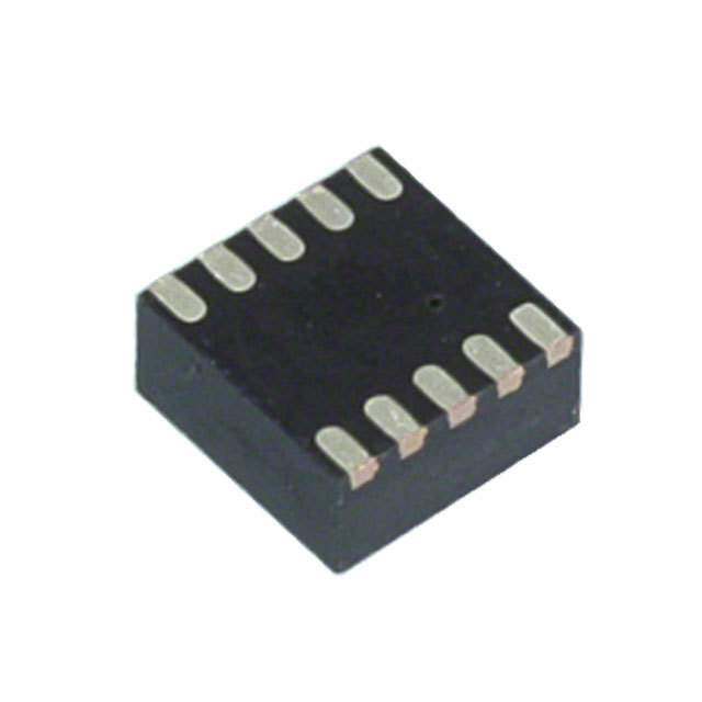
ICGOO电子元器件商城为您提供MAG3110FCR1由Freescale Semiconductor设计生产,在icgoo商城现货销售,并且可以通过原厂、代理商等渠道进行代购。 MAG3110FCR1价格参考。Freescale SemiconductorMAG3110FCR1封装/规格:磁性传感器 - 线性,罗盘(IC), Magnetoresistive Sensor X, Y, Z Axis 10-DFN (2x2)。您可以下载MAG3110FCR1参考资料、Datasheet数据手册功能说明书,资料中有MAG3110FCR1 详细功能的应用电路图电压和使用方法及教程。
NXP USA Inc. 的 MAG3110FCR1 是一款高精度、低功耗的磁性传感器IC,属于线性磁场传感器(电子罗盘)类别。该器件主要用于检测地球磁场,实现三维方向的磁力测量,常用于需要电子罗盘功能的便携式设备中。

其典型应用场景包括:

1. 智能手机与平板电脑:用于实现电子指南针功能,支持地图导航、增强现实(AR)和自动屏幕旋转等应用,提升用户交互体验。

2. 可穿戴设备:如智能手表、运动手环等,结合加速度计进行航位推算(PDR),实现精准的室内定位和运动轨迹追踪。

3. 无人机与遥控模型:提供航向信息,辅助飞行控制系统判断姿态和方向,增强飞行稳定性与导航能力。

4. 物联网终端设备:在智能导航节点或环境感知模块中,用于方向识别与位置服务。

5. 消费类电子产品:如数码相机、游戏控制器等,用于手势识别和空间定位功能。

MAG3110FCR1 具有I²C数字接口,易于集成,工作温度范围宽,抗干扰能力强,适合在复杂电磁环境中稳定运行。配合加速度传感器进行传感器融合,可有效提高方向检测精度,是实现低成本、高性能电子罗盘的理想选择。
| 参数 | 数值 |
| 产品目录 | |
| 描述 | MAGNETOMETER XYZ DIGITAL 10DFN板机接口霍耳效应/磁性传感器 XYZ DIGITAL MAGNETOMETER |
| 产品分类 | 磁性传感器 - 霍尔效应,数字开关,线性,罗盘 (IC)磁性传感器 |
| 品牌 | Freescale Semiconductor |
| 产品手册 | http://cache.freescale.com/webapp/sps/site/prod_summary.jsp?code=MAG3110&tab=Documentation_Tab&linkline=Data%20Sheets&fpsp=1&OrderablePart=MAG3110FCR1 |
| 产品图片 |
|
| rohs | 符合RoHS无铅 / 符合限制有害物质指令(RoHS)规范要求 |
| 产品系列 | 板机接口霍耳效应/磁性传感器,Freescale Semiconductor MAG3110FCR1- |
| 数据手册 | 点击此处下载产品Datasheet点击此处下载产品Datasheet点击此处下载产品Datasheet点击此处下载产品Datasheet |
| 产品型号 | MAG3110FCR1 |
| 产品培训模块 | http://www.digikey.cn/PTM/IndividualPTM.page?site=cn&lang=zhs&ptm=26057http://www.digikey.cn/PTM/IndividualPTM.page?site=cn&lang=zhs&ptm=26056 |
| 产品种类 | 板机接口霍耳效应/磁性传感器 |
| 供应商器件封装 | 10-DFN(2x2) |
| 其它名称 | MAG3110FCR1DKR |
| 包装 | Digi-Reel® |
| 单位重量 | 6.700 mg |
| 商标 | Freescale Semiconductor |
| 安装风格 | SMD/SMT |
| 封装 | Reel |
| 封装/外壳 | 10-VFDFN |
| 封装/箱体 | DFN2020-10 |
| 工作温度 | -40°C ~ 85°C |
| 工作点最小值/最大值 | +/- 1000 uT |
| 工作电源电压 | 1.95 V to 3.6 V |
| 工厂包装数量 | 1000 |
| 感应范围 | ±1000µT |
| 最大工作温度 | + 85 C |
| 最小工作温度 | - 40 C |
| 标准包装 | 1 |
| 特性 | - |
| 电压-电源 | 1.95 V ~ 3.6 V |
| 电流-电源 | 900µA |
| 电流-输出(最大值) | - |
| 电源电流 | 900 uA |
| 类型 | 数字磁力计 |
| 系列 | MAG3110 |
| 输出类型 | 数字 - I²C |


- 商务部:美国ITC正式对集成电路等产品启动337调查
- 曝三星4nm工艺存在良率问题 高通将骁龙8 Gen1或转产台积电
- 太阳诱电将投资9.5亿元在常州建新厂生产MLCC 预计2023年完工
- 英特尔发布欧洲新工厂建设计划 深化IDM 2.0 战略
- 台积电先进制程称霸业界 有大客户加持明年业绩稳了
- 达到5530亿美元!SIA预计今年全球半导体销售额将创下新高
- 英特尔拟将自动驾驶子公司Mobileye上市 估值或超500亿美元
- 三星加码芯片和SET,合并消费电子和移动部门,撤换高东真等 CEO
- 三星电子宣布重大人事变动 还合并消费电子和移动部门
- 海关总署:前11个月进口集成电路产品价值2.52万亿元 增长14.8%


PDF Datasheet 数据手册内容提取
Freescale Semiconductor Document Number: MAG3110 Data Sheet: Technical Data Rev. 9.2, 02/2013 An Energy Efficient Solution by Freescale Xtrinsic MAG3110 Three-Axis, Digital Magnetometer MAG3110 Freescale’s MAG3110 is a small, low-power, digital 3-axis magnetometer. The device can be used in conjunction with a 3-axis accelerometer to realize an Top and Bottom View orientation independent electronic compass that can provide accurate heading information. It features a standard I2C serial interface output and smart embedded functions. The MAG3110 is capable of measuring magnetic fields with an output data rate (ODR) up to 80 Hz; these output data rates correspond to sample intervals from 12.5 ms to several seconds. The MAG3110 is available in a plastic DFN package and it is guaranteed to operate over the extended temperature range of -40°C to +85°C. 10-PIN DFN Features 2 mm x 2 mm x 0.85 mm • 1.95 V to 3.6 V supply voltage (VDD) CASE 2154-02 • 1.62 V to VDD IO voltage (VDDIO) • Ultra small 2 mm x 2 mm x 0.85 mm, 0.4 mm pitch, 10-pin package Top View • Full-scale range ±1000 T • Sensitivity of 0.10 T • Noise down to 0.25 T rms Cap-A 1 10 GND • Output Data Rates (ODR) up to 80 Hz VDD 2 9 INT1 • 400 kHz Fast Mode compatible I2C interface NC 3 8 VDDIO • Low-power, single-shot measurement mode Cap-R 4 7 SCL • RoHS compliant GND 5 6 SDA Applications • Electronic Compass (e-compass) Pin Connections • Location-Based Services Ruggedized Target markets • Smartphones, personal navigation devices, robotics, UAVs, speed sensing, current sensing and wrist watches with embedded electronic compasses (e-compass) function. Table1. Ordering information Part number I2C Address Package description Shipping MAG3110FCR1 0x0E DFN-10 Tape and Reel (1000) FXMS3110CDR1 0x0F DFN-10 Tape and Reel (1000) ©2011-2013 Freescale Semiconductor, Inc. All rights reserved.
Contents 1 Block diagram and pin description . . . . . . . . . . . . . . . . . . . . . . . . . . . . . . . . . . . . . . . . . . . . . . . . . . . . . . . . . . . . . . . . . 3 1.1 Application circuit. . . . . . . . . . . . . . . . . . . . . . . . . . . . . . . . . . . . . . . . . . . . . . . . . . . . . . . . . . . . . . . . . . . . . . . . . . . . 4 2 Operating and Electrical Specifications . . . . . . . . . . . . . . . . . . . . . . . . . . . . . . . . . . . . . . . . . . . . . . . . . . . . . . . . . . . . . 5 2.1 Operating characteristics. . . . . . . . . . . . . . . . . . . . . . . . . . . . . . . . . . . . . . . . . . . . . . . . . . . . . . . . . . . . . . . . . . . . . . 5 2.2 Absolute maximum ratings . . . . . . . . . . . . . . . . . . . . . . . . . . . . . . . . . . . . . . . . . . . . . . . . . . . . . . . . . . . . . . . . . . . . 6 2.3 Electrical characteristics . . . . . . . . . . . . . . . . . . . . . . . . . . . . . . . . . . . . . . . . . . . . . . . . . . . . . . . . . . . . . . . . . . . . . . 7 2.4 I2C Interface characteristics. . . . . . . . . . . . . . . . . . . . . . . . . . . . . . . . . . . . . . . . . . . . . . . . . . . . . . . . . . . . . . . . . . . . 8 2.5 I2C pullup resistor selection. . . . . . . . . . . . . . . . . . . . . . . . . . . . . . . . . . . . . . . . . . . . . . . . . . . . . . . . . . . . . . . . . . . . 9 3 Modes of Operation. . . . . . . . . . . . . . . . . . . . . . . . . . . . . . . . . . . . . . . . . . . . . . . . . . . . . . . . . . . . . . . . . . . . . . . . . . . . . 10 4 Functionality. . . . . . . . . . . . . . . . . . . . . . . . . . . . . . . . . . . . . . . . . . . . . . . . . . . . . . . . . . . . . . . . . . . . . . . . . . . . . . . . . . . 10 4.1 Factory calibration. . . . . . . . . . . . . . . . . . . . . . . . . . . . . . . . . . . . . . . . . . . . . . . . . . . . . . . . . . . . . . . . . . . . . . . . . . 10 4.2 Digital interface . . . . . . . . . . . . . . . . . . . . . . . . . . . . . . . . . . . . . . . . . . . . . . . . . . . . . . . . . . . . . . . . . . . . . . . . . . . . 10 5 Register Descriptions . . . . . . . . . . . . . . . . . . . . . . . . . . . . . . . . . . . . . . . . . . . . . . . . . . . . . . . . . . . . . . . . . . . . . . . . . . . 15 5.1 Sensor Status . . . . . . . . . . . . . . . . . . . . . . . . . . . . . . . . . . . . . . . . . . . . . . . . . . . . . . . . . . . . . . . . . . . . . . . . . . . . . 16 5.2 Device ID. . . . . . . . . . . . . . . . . . . . . . . . . . . . . . . . . . . . . . . . . . . . . . . . . . . . . . . . . . . . . . . . . . . . . . . . . . . . . . . . . 18 5.3 User Offset Correction. . . . . . . . . . . . . . . . . . . . . . . . . . . . . . . . . . . . . . . . . . . . . . . . . . . . . . . . . . . . . . . . . . . . . . . 18 5.4 Temperature . . . . . . . . . . . . . . . . . . . . . . . . . . . . . . . . . . . . . . . . . . . . . . . . . . . . . . . . . . . . . . . . . . . . . . . . . . . . . . 19 5.5 Control Registers. . . . . . . . . . . . . . . . . . . . . . . . . . . . . . . . . . . . . . . . . . . . . . . . . . . . . . . . . . . . . . . . . . . . . . . . . . . 19 6 Geomagnetic Field Maps. . . . . . . . . . . . . . . . . . . . . . . . . . . . . . . . . . . . . . . . . . . . . . . . . . . . . . . . . . . . . . . . . . . . . . . . . 22 7 PCB Guidelines . . . . . . . . . . . . . . . . . . . . . . . . . . . . . . . . . . . . . . . . . . . . . . . . . . . . . . . . . . . . . . . . . . . . . . . . . . . . . . . . 24 7.1 Overview of Soldering Considerations. . . . . . . . . . . . . . . . . . . . . . . . . . . . . . . . . . . . . . . . . . . . . . . . . . . . . . . . . . . 24 7.2 Halogen Content . . . . . . . . . . . . . . . . . . . . . . . . . . . . . . . . . . . . . . . . . . . . . . . . . . . . . . . . . . . . . . . . . . . . . . . . . . . 24 7.3 PCB Mounting Recommendations. . . . . . . . . . . . . . . . . . . . . . . . . . . . . . . . . . . . . . . . . . . . . . . . . . . . . . . . . . . . . . 24 Related Documentation The MAG3110 device features and operations are described in a variety of reference manuals, user guides, and application notes. To find the most-current versions of these documents: 1. Go to the Freescale homepage at: http://www.freescale.com/ 2. In the Keyword search box at the top of the page, enter the device number MAG3110. 3. In the Refine Your Result pane on the left, click on the Documentation link. Sensors 2 Freescale Semiconductor, Inc.
1 Block diagram and pin description SDA X-axis SCL Digital Signal Y-axis MUX ADC Processing and Control INT1 Z-axis VDD Regulator Clock Oscillator Trim Logic + VDDIO Reference Figure1. Block diagram 1 X Cap-A 1 10 GND VDD 2 9 INT1 Y NC 3 8 VDDIO Cap-R 4 7 SCL GND 5 6 SDA Z (TOP VIEW) (TOP VIEW) Figure2. Pin connections and measurement coordinate system MAG LYW L = WAFER LOT Y = LAST DIGIT OF YEAR W = WORK WEEK Figure3. Device marking diagram MAG3110 Sensors Freescale Semiconductor, Inc. 3
Table2. Pin descriptions Pin Name Function 1 Cap-A Bypass cap for internal regulator 2 VDD Power supply, 1.95 V – 3.6 V 3 NC Do not connect 4 Cap-R Magnetic reset pulse circuit capacitor connection 5 GND GND 6 SDA I2C Serial Data 7 SCL I2C Serial Clock 8 VDDIO Digital interface supply, 1.65 V - VDD 9 INT1 Interrupt - active high output 10 GND GND 1.1 Application circuit Device power is supplied through the VDD line. Power supply decoupling capacitors (100 nF ceramic) should be placed as near as possible to pins 1 and 2 of the device. Additionally a 1F (or larger) capacitor should be used for bulk decoupling of the VDD supply rail as shown in Figure4. VDDIO supplies power for the digital I/O pins SCL, SDA, and INT1. The control signals SCL and SDA, are not tolerant of voltages more than VDDIO + 0.3 volts. If VDDIO is removed, the control signals SCL and SDA will clamp any logic signals through their internal ESD protection diodes. 1 Cap-A GND 10 100 nF 2 VDD INT1 9 INT1 VDDIO 3 NC VDDIO 8 100 nF 4.7 K 4.7 K VDD 4 Cap-R SCL 7 SCL 1 F 100 nF 100 nF 5 GND SDA 6 SDA (Top view) Figure4. Electrical connection MAG3110 Sensors 4 Freescale Semiconductor, Inc.
2 Operating and Electrical Specifications 2.1 Operating characteristics Table3. Operating characteristics @ VDD = 2.4 V, VDDIO = 1.8 V, T = 25°C unless otherwise noted. Parameter Test Conditions Symbol Min Typ Max Unit Full-scale range FS ±1000 µT Output data range(1) -30000 +30000 LSB Sensitivity So 0.10 µT/LSB Sensitivity change versus temperature Tcs ±0.1 %/°C Zero-flux offset accuracy ±100 µT Hysteresis(2) 0.25 1 % Non linearity Best fit straight line(3) NL -1 ±0.3 1 %FS Magnetometer output noise OS = 00(4) 0.4 OS = 01 0.35 Noise µT rms OS = 10 0.3 OS = 11 0.25 Sensor die-to-package misalignment error (yaw) D2PE ±0.37 ±1.36 degrees yaw Operating temperature range T -40 +85 °C op 1. Output data range is the sum of ±10000 LSBs full-scale range, ±10000 LSBs user defined offset (provided that CTRL_REG2[RAW] = 0) and ±10000 zero-flux offset. 2.Hysteresis is measured from 0 T to 1000 T to 0 T and from 0 T to -1000 T to 0 T. 3.Best-fit straight line over the 0 to ±1000 T full-scale range. 4.OS = Over Sampling Ratio. MAG3110 Sensors Freescale Semiconductor, Inc. 5
2.2 Absolute maximum ratings Stresses above those listed as “absolute maximum ratings” may cause permanent damage to the device. This is a stress rating only and functional operation of the device under these conditions is not implied. Exposure to maximum rating conditions for extended periods may affect device reliability. Table4. Maximum ratings Rating Symbol Value Unit Supply voltage VDD -0.3 to +3.6 V Input voltage on any control pin (SCL, SDA) Vin -0.3 to VDDIO + 0.3 V Maximum applied magnetic/field B 100,000 µT MAX Operating temperature range T -40 to +85 °C op Storage temperature range T -40 to +125 °C STG Table5. ESD and latchup protection characteristics Rating Symbol Value Unit Human Body Model HBM ±2000 V Machine Model MM ±200 V Charge Device Model CDM ±500 V Latchup current at T = 85°C I ±100 mA LU This device is sensitive to mechanical shock. Improper handling can cause permanent damage of the part or cause the part to otherwise fail. This device is sensitive to ESD, improper handling can cause permanent damage to the part. MAG3110 Sensors 6 Freescale Semiconductor, Inc.
2.3 Electrical characteristics Table6. Electrical characteristics @ VDD = 2.4 V, VDDIO = 1.8 V, T = 25°C unless otherwise noted Parameter Test Conditions Symbol Min Typ Max Unit Supply voltage VDD 1.95 2.4 3.6 V Interface supply voltage VDDIO 1.62 VDD V Supply current in ACTIVE mode ODR(1)(2) 80 Hz, OS(1) = 00 900 ODR 40 Hz, OS(3) = 00 550 ODR 20 Hz, OS(3) = 00 275 ODR 10 Hz, OS(3) = 00 137.5 I µA dd ODR 5 Hz, OS(3) = 00 68.8 ODR 2.5 Hz, OS(3) = 00 34.4 ODR 1.25 Hz, OS(3) = 00 17.2 ODR 0.63 Hz, OS = 00 8.6 Supply current drain in STANDBY mode Measurement mode off I Stby 2 µA dd Digital high level input voltage V SCL, SDA VIH 0.75*VDDIO Digital low level input voltage V SCL, SDA VIL 0.3* VDDIO High level output voltage I = 500 µA V INT1 O VOH 0.9*VDDIO Low level output voltage I = 500 µA V INT1 O VOL 0.1* VDDIO Low level output voltage I = 500 µA 0.1* VDDIO V SDA O VOLS Output Data Rate (ODR) ODR 0.8*ODR ODR 1.2 *ODR Hz Signal bandwidth BW ODR/2 Hz Boot time from power applied to boot complete BT 1.7 ms Turn-on time(4)(5) CTRL_REG1[OS] = 2'b01 Ton 25 ms Operating temperature range T -40 +85 °C op 1.ODR = Output Data Rate; OS = Over Sampling Ratio. 2.Please see Table32 for all ODR and OSR setting combinations, as well as corresponding current consumption and noise levels. 3.By design. 4.Time to obtain valid data from STANDBY mode to ACTIVE Mode. 5.In 80 Hz mode ODR. MAG3110 Sensors Freescale Semiconductor, Inc. 7
2.4 I2C Interface characteristics Table7. I2C slave timing values(1) I2C Fast Mode Parameter Symbol Unit Min Max SCL clock frequency f Pullup = 1 k C = 20 pF SCL 0 400 kHz b Bus free time between STOP and START condition t 1.3 s BUF Repeated START hold time t 0.6 s HD;STA Repeated START setup time t 0.6 s SU;STA STOP condition setup time t 0.6 s SU;STO SDA data hold time(2) t 0.05(3) (4) s HD;DAT SDA valid time(5) t 0.9(4) s VD;DAT SDA valid acknowledge time(6) t 0.9(4) s VD;ACK SDA setup time t 100(7) ns SU;DAT SCL clock low time t 1.3 s LOW SCL clock high time t 0.6 s HIGH SDA and SCL rise time t 20 + 0.1C (8) 1000 ns r b SDA and SCL fall time(3) (8) (9) (10) t 20 + 0.1C (8) 300 ns f b Pulse width of spikes on SDA and SCL that must be suppressed by input filter t 50 ns SP 1.All values are referred to VIH (min) and VIL (max) levels. 2.t is the data hold time that is measured from the falling edge of SCL; the hold time applies to data in transmission and the acknowledge. HD;DAT 3.A device must internally provide a hold time of at least 300 ns for the SDA signal (with respect to the VIH (min) of the SCL signal) to bridge the undefined region of the falling edge of SCL. 4.The maximum t could be must be less than the maximum of t or t by a transition time. This device may stretch the LOW HD;DAT VD;DAT VD;ACK period (t ) of the SCL signal. LOW 5.t = time for Data signal from SCL LOW to SDA output (HIGH or LOW, depending on which one is worse). VD;DAT 6.t = time for Acknowledgement signal from SCL LOW to SDA output (HIGH or LOW, depending on which one is worse). VD;ACK 7.A Fast mode I2C device can be used in a Standard mode I2C system, but the requirement t 250 ns must then be met. This will SU;DAT automatically be the case if the device does not stretch the LOW period of the SCL signal. If such a device does stretch the LOW period of the SCL signal, it must output the next data bit to the SDA line t(max) + t = 1000 + 250 = 1250 ns (according to the Standard mode I2C r SU;DAT specification) before the SCL line is released. Also the acknowledge timing must meet this setup time. 8.C = total capacitance of one bus line in pF. b 9.The maximum t for the SDA and SCL bus lines is specified at 300 ns. The maximum fall time for the SDA output stage t is specified at 250ns. f f This allows series protection resistors to be connected in between the SDA and the SCL pins and the SDA/SCL bus lines without exceeding the maximum specified t. f 10.In Fast mode Plus, fall time is specified the same for both output stage and bus timing. If series resistors are used, designers should allow for this when considering bus timing. MAG3110 Sensors 8 Freescale Semiconductor, Inc.
Figure5. I2C slave timing diagram 2.5 I2C pullup resistor selection The SCL and SDA signals are driven by open-drain buffers and a pullup resistor is required to make the signals rise to the high state. The value of the pullup resistors depends on the system I2C clock rate and the total capacitive load on the I2C bus. Higher resistance pullups will conserve power, at the expense of a slower rise time on the SCL and SDA lines (due to the RC time constant between the bus capacitance and the pullup resistor), and will limit the maximum I2C clock frequency that can be achieved. Lower resistance value pullup resistors consume more power, but enable higher I2C clock operating frequencies. I2C bus capacitance consists of the sum of the parasitic device and trace capacitances present. In general, longer bus traces and an increased number of devices lead to higher total bus capacitance and will require lower value pullup resistors to enable a given frequency of operation. For Standard mode operation, pullup resistor values between 5 k and 10 k are recommended as a starting point, but may need to be lowered depending on the number of devices present on the bus and the total bus capacitance. For Fast mode operation, pullup resistor values of 1k (or lower) may be required. MAG3110 Sensors Freescale Semiconductor, Inc. 9
3 Modes of Operation Table8. Modes of operation description Mode I2C Bus State Function Description STANDBY I2C communication is possible. Only POR and Digital blocks are enabled, the Analog subsystem is disabled. ACTIVE I2C communication is possible. All blocks are enabled (POR, Digital, Analog). 4 Functionality MAG3110 is a small low-power, digital output, 3-axis linear magnetometer packaged in a 10-pin DFN. The device contains a magnetic transducer for sensing and an ASIC for control and digital I2C communications. 4.1 Factory calibration MAG3110 is factory calibrated for sensitivity and temperature coefficient of sensitivity. All factory calibration coefficients are automatically applied by the ASIC before a measurement is taken and the result written to registers 0x01 to 0x06 (Section5, “Register Descriptions,” on page15). The magnetic offset registers in addresses 0x09 to 0x0E are not a factory calibration offset but allow the user to define a hard- iron offset which can be automatically subtracted from the magnetic field readings (see Section4.2.4, “User offset corrections,” on page12). 4.2 Digital interface Table9. Serial interface pin description Pin name Pin description VDDIO IO voltage SCL I2C Serial Clock SDA I2C Serial Data INT Data ready interrupt pin There are two signals associated with the I2C bus: the Serial Clock Line (SCL) and the Serial Data line (SDA). External pullup resistors (connected to VDDIO) are needed for SDA and SCL. When the bus is free, both lines are high. The I2C interface is compliant with Fast mode (400 kHz), and Normal mode (100 kHz) I2C standards. 4.2.1 General I2C operation There are two signals associated with the I2C bus: the Serial Clock Line (SCL) and the Serial Data line (SDA). The latter is a bidirectional line used for sending and receiving the data to/from the interface. External pullup resistors connected to VDDIO are required for SDA and SCL. When the bus is free both the lines are high. The I2C interface is compliant with fast mode (400kHz), and normal mode (100 kHz) I2C standards. Operation at frequencies higher than 400 kHz is possible, but depends on several factors including the pullup resistor values, and total bus capacitance (trace + device capacitance). A transaction on the bus is started with a start condition (ST) signal, which is defined as a HIGH-to-LOW transition on the data line while the SCL line is held HIGH. After the ST signal has been transmitted by the master, the bus is considered busy. The next byte of data transmitted contains the slave address in the first seven bits, and the eighth bit, the read/write bit, indicates whether the master is receiving data from the slave or transmitting data to the slave. When an address is sent, each device in the system compares the first seven bits after the ST condition with its own address. If they match, the device considers itself addressed by the master. The 9th clock pulse, following the slave address byte (and each subsequent byte) is the acknowledge (ACK). The transmitter must release the SDA line during the ACK period. The receiver must then pull the data line low so that it remains stable low during the high period of the acknowledge clock period. The number of bytes per transfer is unlimited. If a receiver can't receive another complete byte of data until it has performed some other function, it can hold the clock line, SCL low to force the transmitter into a wait state. Data transfer only continues when the receiver is ready for another byte and releases the data line. This delay action is called clock stretching. Not all receiver devices support clock stretching. Not all master devices recognize clock stretching. This part supports clock stretching. MAG3110 Sensors 10 Freescale Semiconductor, Inc.
A low to high transition on the SDA line while the SCL line is high is defined as a stop condition (SP) signal. A write or burst write is always terminated by the master issuing the SP signal. A master should properly terminate a read by not acknowledging a byte at the appropriate time in the protocol. A master may also issue a repeated start signal (SR) during a transfer. The 7-bit I2C slave address assigned to MAG3110 is 0x0E (standard); the address assigned to FXMS3110CD is 0x0F (Windows™ 8). 4.2.2 I2C Read/Write operations Single byte read The master (or MCU) transmits a start condition (ST) to the MAG3110, followed by the slave address, with the R/W bit set to “0” for a write, and the MAG3110 sends an acknowledgement. Then the master (or MCU) transmits the address of the register to read and the MAG3110 sends an acknowledgement. The master (or MCU) transmits a repeated start condition (SR), followed by the slave address with the R/W bit set to “1” for a read from the previously selected register. The MAG3110 then acknowledges and transmits the data from the requested register. The master does not acknowledge (NAK) the transmitted data, but transmits a stop condition to end the data transfer. Multiple byte read When performing a multi-byte or “burst” read, the MAG3110 automatically increments the register address read pointer after a read command is received. Therefore, after following the steps of a single byte read, multiple bytes of data can be read from sequential registers after each MAG3110 acknowledgment (AK) is received until a no acknowledge (NAK) occurs from the master followed by a stop condition (SP) signaling the end of transmission. Single byte write To start a write command, the master transmits a start condition (ST) to the MAG3110, followed by the slave address with the R/W bit set to “0” for a write, and the MAG3110 sends an acknowledgement. Then the master (or MCU) transmits the address of the register to write to, and the MAG3110 sends an acknowledgement. Then the master (or MCU) transmits the 8-bit data to write to the designated register and the MAG3110 sends an acknowledgement that it has received the data. Since this transmission is complete, the master transmits a stop condition (SP) to end the data transfer. The data sent to the MAG3110 is now stored in the appropriate register. Multiple byte write The MAG3110 automatically increments the register address write pointer after a write command is received. Therefore, after following the steps of a single byte write, multiple bytes of data can be written to sequential registers after each MAG3110 acknowledgment (ACK) is received. MAG3110 Sensors Freescale Semiconductor, Inc. 11
< Single Byte Read > Master ST Device Address[6:0] W Register Address[7:0] SR Device Address[6:0] R NAK SP Slave AK AK AK Data[7:0] < Multiple Byte Read > Master ST Device Address[6:0] W Register Address[7:0] SR Device Address[6:0] R AK Slave AK AK AK Data[7:0] Master AK AK NAK SP Slave Data[7:0] Data[7:0] Data[7:0] < Multiple Byte Write > Master ST Device Address[6:0] W Register Address[7:0] Data[7:0] Data[7:0] SP Slave AK AK AK AK < Single Byte Write > Master ST Device Address[6:0] W Register Address[7:0] Data[7:0] SP Slave AK AK AK Legend ST: Start Condition SP: Stop Condition NAK: No Acknowledge W: Write = 0 SR: Repeated Start Condition AK: Acknowledge R: Read = 1 Figure6. I2C timing diagram 4.2.3 Fast Read mode When the Fast Read (FR) bit is set (CTRL_REG1, 0x10, bit 2), the MSB 8-bit data is read through the I2C bus. Auto-increment is set to skip over the LSB data. When FR bit is cleared, the complete 16-bit data is read accessing all 6 bytes sequentially (OUT_X_MSB, OUT_X_LSB, OUT_Y_MSB, OUT_Y_LSB, OUT_Z_MSB, OUT_Z_LSB). 4.2.4 User offset corrections The 2’s complement user offset correction register values are used to compensate for correcting the X, Y, and Z-axis after device board mount. These values may be used to compensate for hard-iron interference and zero-flux offset of the sensor. Depending on the setting of the CTRL_REG2[RAW] bit, the magnetic field sample data is corrected with the user offset values (CTRL_REG2[RAW] = 0), or can be read out uncorrected for user offset values (CTRL_REG2[RAW] = 1). The factory calibration for gain, offset and temperature compensation is always automatically applied irrespective of the setting of the CTRL_REG2[RAW] bit which only controls whether the user offset correction values stored in the OFF_X/Y/Z registers are applied to the output data. In order to not saturate the sensor output, user written offset values should be within the range of ±10,000 counts. MAG3110 Sensors 12 Freescale Semiconductor, Inc.
4.2.5 INT1 The DR_STATUS register (see section 5.1.1) contains the ZYXDR bit which denotes the presence of new measurement data on one or more axes. Software polling can be used to detect the transition of the ZYXDR bit from 0 to 1 but, since the ZYXDR bit is also logically connected to the INT1 pin, a more efficient approach is to use INT1 to trigger a software interrupt when new measurement data is available as follows: 1. Enable automatic resets by setting AUTO_MRST_EN bit in CTRL_REG2 (CTRL_REG2 = 0b1XXXXXX). 2. Put MAG3110 in ACTIVE mode (CTRL_REG1 = 0bXXXXXX01). 3. Idle until INT1 goes HIGH and activates an interrupt service routine in the user software. 4. Read magnetometer data as required from registers 0x01 to 0x06. INT1 is cleared when register 0x01 OUT_X_MSB is read. 5. Return to idle in step 3. 4.2.6 Triggered Measurements Set the TM bit in CTRL_REG1 when you want the part to acquire only one sample on each axis. See table below for details. Table10. AC TM Description 0 0 ASIC is in low power standby mode. The ASIC will exit standby mode, perform one measurement cycle based on the 0 1 programmed ODR and OSR setting, update the I2C data registers and re- enter standby mode. The ASIC will perform continuous measurements based on the current OSR and 1 0 ODR settings. The ASIC will continue the current measurement at the fastest applicable ODR 1 1 for the user programmed OSR. The ASIC will return back to the programmed ODR after completing the triggered measurement. The anti-aliasing filter in the A/D converter has a finite delay before the output “settles”. The output data for the first ODR period after getting out of Standby mode is expected to be slightly off. This effect will be more pronounced for the lower over-sampling settings since with higher settings the error of the first acquisition will be averaged over the total number of samples. Therefore, it is not recommended to use TRIGGER MODE (CTRL_REG1[AC] =0, CTRL_REG1[TM] =1) measurements for applications that require high accuracy, especially with low over-sampling settings. MAG3110 Sensors Freescale Semiconductor, Inc. 13
4.2.7 MAG3110 Setup Examples Continuous measurements with ODR = 80 Hz, OSR = 1 1. Enable automatic magnetic sensor resets by setting bit AUTO_MRST_EN in CTRL_REG2. (CTRL_REG2 = 0x80) 2. Put MAG3110 in active mode 80 Hz ODR with OSR = 1 by writing 0x01 to CTRL_REG1 (CTRL_REG1 = 0x01) 3. At this point it is possible to sync with MAG3110 utilizing INT1 pin or using polling of the DR_STATUS register as explained in section 4.2.5. Continuous measurements with ODR = 0.63 Hz, OSR = 2 1. Enable automatic magnetic sensor resets by setting bit AUTO_MRST_EN in CTRL_REG2. (CTRL_REG2 = 0x80) 2. Put MAG3110 in active mode 0.63 Hz ODR with OSR = 2 by writing 0xC9 to CTRL_REG1 (CTRL_REG1 = 0xC9) 3. At this point, it is possible to sync with MAG3110 utilizing INT1 pin or using polling of the DR_STATUS register as explained in section 4.2.5. Triggered measurements with ODR = 10 Hz, OSR = 8 1. Enable automatic magnetic sensor resets by setting bit AUTO_MRST_EN in CTRL_REG2. (CTRL_REG2 = 0x80) 2. Initiate a triggered measurement with OSR = 128 by writing 0b00011010 to CTRL_REG1 (CTRL_REG1 = 0b00011010). 3. MAG3110 will acquire the triggered measurement and go back into STANDBY mode. It is possible at this point to sync on INT1 or resort to polling of DR_STATUS register to read the acquired data out of MAG3110. 4. Go back to step 2 based on application needs. MAG3110 Sensors 14 Freescale Semiconductor, Inc.
5 Register Descriptions Table11. Register Address Map Register Auto-Increment Name Type Default Value Comment Address Address (Fast Read)(1) DR_STATUS(2) R 0x00 0x01 0000 0000 Data ready status per axis OUT_X_MSB(2) R 0x01 0x02 (0x03) data Bits [15:8] of X measurement OUT_X_LSB(2) R 0x02 0x03 data Bits [7:0] of X measurement OUT_Y_MSB(2) R 0x03 0x04 (0x05) data Bits [15:8] of Y measurement OUT_Y_LSB(2) R 0x04 0x05 data Bits [7:0] of Y measurement OUT_Z_MSB(2) R 0x05 0x06 (0x07) data Bits [15:8] of Z measurement OUT_Z_LSB(2) R 0x06 0x07 data Bits [7:0] of Z measurement WHO_AM_I(2) R 0x07 0x08 0xC4 Device ID Number SYSMOD(2) R 0x08 0x09 data Current System Mode OFF_X_MSB R/W 0x09 0x0A 0000 0000 Bits [14:7] of user X offset OFF_X_LSB R/W 0x0A 0x0B 0000 0000 Bits [6:0] of user X offset OFF_Y_MSB R/W 0x0B 0x0C 0000 0000 Bits [14:7] of user Y offset OFF_Y_LSB R/W 0x0C 0x0D 0000 0000 Bits [6:0] of user Y offset OFF_Z_MSB R/W 0x0D 0x0E 0000 0000 Bits [14:7] of user Z offset OFF_Z_LSB R/W 0x0E 0x0F 0000 0000 Bits [6:0] of user Z offset DIE_TEMP(2) R 0x0F 0x10 data Temperature, signed 8 bits in (cid:31)C CTRL_REG1(3) R/W 0x10 0x11 0000 0000 Operation modes CTRL_REG2(3) R/W 0x11 0x12 0000 0000 Operation modes 1.Fast Read mode for quickly reading the Most Significant Bytes (MSB) of the sampled data. 2.Register contents are preserved when transitioning from “ACTIVE” to “STANDBY” mode. 3.Modification of this register’s contents can only occur when device is “STANDBY” mode, except the TM and AC bit fields in CTRL_REG1 register. MAG3110 Sensors Freescale Semiconductor, Inc. 15
5.1 Sensor Status 5.1.1 DR_STATUS (0x00) Data Ready Status This read-only status register provides the acquisition status information on a per-sample basis, and reflects real-time updates to the OUT_X, OUT_Y, and OUT_Z registers. Table12. DR_STATUS Register Bit 7 Bit 6 Bit 5 Bit 4 Bit 3 Bit 2 Bit 1 Bit 0 ZYXOW ZOW YOW XOW ZYXDR ZDR YDR XDR Table13. DR_STATUS Descriptions X, Y, Z-axis Data Overwrite. Default value: 0. ZYXOW 0: No data overwrite has occurred. 1: Previous X or Y or Z data was overwritten by new X or Y or Z data before it was completely read. Z-axis Data Overwrite. Default value: 0. ZOW 0: No data overwrite has occurred. 1: Previous Z-axis data was overwritten by new Z-axis data before it was read. Y-axis Data Overwrite. Default value: 0. YOW 0: No data overwrite has occurred. 1: Previous Y-axis data was overwritten by new Y-axis data before it was read. X-axis Data Overwrite. Default value: 0 XOW 0: No data overwrite has occurred. 1: Previous X-axis data was overwritten by new X-axis data before it was read. X or Y or Z-axis new Data Ready. Default value: 0. ZYXDR 0: No new set of data ready. 1: New set of data is ready. Z-axis new Data Available. Default value: 0. ZDR 0: No new Z-axis data is ready. 1: New Z-axis data is ready. Z-axis new Data Available. Default value: 0. YDR 0: No new Y-axis data is ready. 1: New Y-axis data is ready. Z-axis new Data Available. Default value: 0. XDR 0: No new X-axis data is ready. 1: New X-axis data is ready. ZYXOW is set to 1 whenever new data is acquired before completing the retrieval of the previous set. This event occurs when the content of at least one data register (i.e. OUT_X, OUT_Y, OUT_Z) has been overwritten. ZYXOW is cleared when the high- bytes of the data (OUT_X_MSB, OUT_Y_MSB, OUT_Z_MSB) of all active channels are read. ZOW is set to 1 whenever new Z-axis acquisition is completed before the retrieval of the previous data. When this occurs the previous data is overwritten. ZOW is cleared any time OUT_Z_MSB register is read. YOW is set to 1 whenever new Y-axis acquisition is completed before the retrieval of the previous data. When this occurs the previous data is overwritten. YOW is cleared any time OUT_Y_MSB register is read. XOW is set to 1 whenever new X-axis acquisition is completed before the retrieval of the previous data. When this occurs the previous data is overwritten. XOW is cleared any time OUT_X_MSB register is read. ZYXDR signals that new acquisition for any of the enabled channels is available. ZYXDR is cleared when the high-bytes of the data (OUT_X_MSB, OUT_Y_MSB, OUT_Z_MSB) of all the enabled channels are read. ZDR is set to 1 whenever new Z-axis data acquisition is completed. ZDR is cleared any time OUT_Z_MSB register is read. YDR is set to 1 whenever new Y-axis data acquisition is completed. YDR is cleared any time OUT_Y_MSB register is read. XDR is set to 1 whenever new X-axis data acquisition is completed. XDR is cleared any time OUT_X_MSB register is read. MAG3110 Sensors 16 Freescale Semiconductor, Inc.
5.1.2 OUT_X_MSB (0x01), OUT_X_LSB (0x02), OUT_Y_MSB (0x03), OUT_Y_LSB (0x04), OUT_Z_MSB (0x05), OUT_Z_LSB (0x06) X-axis, Y-axis, and Z-axis 16-bit output sample data of the magnetic field strength expressed as signed 2's complement numbers. When RAW bit is set (CTRL_REG2[RAW] = 1), the output range is between -20,000 to 20,000 bit counts (the combination of the 1000T full scale range and the zero-flux offset ranging up to 1000 T). When RAW bit is clear (CTRL_REG2[RAW] = 0), the output range is between -30,000 to 30,000 bit counts when the user offset ranging between -10,000 to 10,000 bit counts are included. The DR_STATUS register, OUT_X_MSB, OUT_X_LSB, OUT_Y_MSB, OUT_Y_LSB, OUT_Z_MSB, and OUT_Z_LSB are stored in the auto-incrementing address range of 0x00 to 0x06. Data acquisition is a sequential read of 6 bytes. If the Fast Read (FR) bit is set in CTRL_REG1 (0x10), auto-increment will skip over LSB of the X, Y, Z sample registers. This will shorten the data acquisition from 6 bytes to 3 bytes. If the LSB registers are directly addressed, the LSB information can still be read regardless of FR bit setting. The preferred method for reading data registers is the burst-read method where the user application acquires data sequentially starting from register 0x01. If register 0x01 is not read first, the rest of the data registers (0x02 - 0x06) will not be updated with the most recent acquisition. It is still possible to address individual data registers, however register 0x01 must be read prior to ensure that the latest acquisition data is being read. Table14. OUT_X_MSB Register Bit 7 Bit 6 Bit 5 Bit 4 Bit 3 Bit 2 Bit 1 Bit 0 XD15 XD14 XD13 XD12 XD11 XD10 XD9 XD8 Table15. OUT_X_LSB Register Bit 7 Bit 6 Bit 5 Bit 4 Bit 3 Bit 2 Bit 1 Bit 0 XD7 XD6 XD5 XD4 XD3 XD2 XD1 XD0 Table16. OUT_Y_MSB Register Bit 7 Bit 6 Bit 5 Bit 4 Bit 3 Bit 2 Bit 1 Bit 0 YD15 YD14 YD13 YD12 YD11 YD10 YD9 YD8 Table17. OUT_Y_LSB Register Bit 7 Bit 6 Bit 5 Bit 4 Bit 3 Bit 2 Bit 1 Bit 0 YD7 YD6 YD5 YD4 YD3 YD2 YD1 YD0 Table18. OUT_Z_MSB Register Bit 7 Bit 6 Bit 5 Bit 4 Bit 3 Bit 2 Bit 1 Bit 0 ZD15 ZD14 ZD13 ZD12 ZD11 ZD10 ZD9 ZD8 Table19. OUT_Z_LSB Register Bit 7 Bit 6 Bit 5 Bit 4 Bit 3 Bit 2 Bit 1 Bit 0 ZD6 ZD6 ZD5 ZD4 ZD3 ZD2 ZD1 ZD0 MAG3110 Sensors Freescale Semiconductor, Inc. 17
5.2 Device ID 5.2.1 WHO_AM_I (0x07) Device identification register. This read-only register contains the device identifier which is set to 0xC4. This value is factory programmed. Table20. WHO_AM_I Register Bit 7 Bit 6 Bit 5 Bit 4 Bit 3 Bit 2 Bit 1 Bit 0 1 1 0 0 0 1 0 0 5.2.2 SYSMOD (0x08) The read-only system mode register indicates the current device operating mode. Table21. SYSMOD Register Bit 7 Bit 6 Bit 5 Bit 4 Bit 3 Bit 2 Bit 1 Bit 0 0 0 0 0 0 0 SYSMOD1 SYSMOD0 Table22. SYSMOD Description System Mode. Default value: 00. 00: STANDBY mode. SYSMOD 01: ACTIVE mode, RAW data. 10: ACTIVE mode, non-RAW user-corrected data. 5.3 User Offset Correction 5.3.1 OFF_X_MSB (0x09), OFF_X_LSB (0x0A), OFF_Y_MSB (0x0B), OFF_Y_LSB (0x0C), OFF_Z_MSB (0x0D), OFF_Z_LSB (0x0E) These registers contain the X-axis, Y-axis, and Z-axis user defined offsets in 2's complement format which are used when CTRL_REG2[RAW] = 0 (see section 5.5.2) to correct for the MAG3110 zero-flux offset and for hard-iron offsets on the PCB caused by external components. The maximum range for the user offsets is in the range -10,000 to 10,000 bit counts comprising the sum of the correction for the sensor zero-flux offset and the PCB hard-iron offset (range -1000 T to 1000 T or -10,000 to 10,000 bit counts). The user offsets are automatically subtracted by the MAG3110 logic when CTRL_REG2[RAW] = 0 before the magnetic field readings are written to the data measurement output registers OUT_X/Y/Z. The maximum range of the X, Y and Z data measurement registers when CTRL_REG2[RAW] = 0 is therefore -30,000 to 30,000 bit counts and is computed without clipping. The user offsets are not subtracted when CTRL_REG2[RAW] = 1. The least significant bit of the user defined X, Y and Z offsets is forced to be zero irrespective of the value written by the user. If the MAG3110 zero-flux offset and PCB hard-iron offset corrections are performed by an external microprocessor (the most likely scenario) then the user offset registers can be ignored and the CTRL_REG2[RAW] bit should be set to 1. The user offset registers should not be confused with the factory calibration corrections which are not user accessible and are always applied to the measured magnetic data irrespective o the setting of CTRL_REG2[RAW]. Table23. OFF_X_MSB Register Bit 7 Bit 6 Bit 5 Bit 4 Bit 3 Bit 2 Bit 1 Bit 0 XD14 XD13 XD12 XD11 XD10 XD9 XD8 XD7 Table24. OFF_X_LSB Register Bit 7 Bit 6 Bit 5 Bit 4 Bit 3 Bit 2 Bit 1 Bit 0 XD6 XD5 XD4 XD3 XD2 XD1 XD0 0 Table25. OFF_Y_MSB Register Bit 7 Bit 6 Bit 5 Bit 4 Bit 3 Bit 2 Bit 1 Bit 0 YD14 YD13 YD12 YD11 YD10 YD9 YD8 YD7 MAG3110 Sensors 18 Freescale Semiconductor, Inc.
Table26. OFF_Y_LSB Register Bit 7 Bit 6 Bit 5 Bit 4 Bit 3 Bit 2 Bit 1 Bit 0 YD6 YD5 YD4 YD3 YD2 YD1 YD0 0 Table27. OFF_Z_MSB Register Bit 7 Bit 6 Bit 5 Bit 4 Bit 3 Bit 2 Bit 1 Bit 0 ZD14 ZD13 ZD12 ZD11 ZD10 ZD9 ZD8 ZD7 Table28. OFF_Z_LSB Register Bit 7 Bit 6 Bit 5 Bit 4 Bit 3 Bit 2 Bit 1 Bit 0 ZD6 ZD5 ZD4 ZD3 ZD2 ZD1 ZD0 0 5.4 Temperature 5.4.1 DIE_TEMP (0x0F) The register contains the die temperature in °C expressed as an 8-bit 2's complement number. The sensitivity of the temperature sensor is factory trimmed to 1°C/LSB. The temperature sensor offset is not factory trimmed and must be calibrated by the user software if higher absolute accuracy is required. Note: The register allows for temperature measurements from -128°C to 127°C but the output range is limited to -40°C to 125°C. The temperature data is updated on every measurement cycle. Table29. TEMP Register Bit 7 Bit 6 Bit 5 Bit 4 Bit 3 Bit 2 Bit 1 Bit 0 T7 T6 T5 T4 T3 T2 T1 T0 5.5 Control Registers 5.5.1 CTRL_REG1 (0x10) Note: Except for STANDBY mode selection (Bit 0, AC), the device must be in STANDBY mode to change any of the fields within CTRL_REG1 (0x10). Table30. CTRL_REG1 Register Bit 7 Bit 6 Bit 5 Bit 4 Bit 3 Bit 2 Bit 1 Bit 0 DR2 DR1 DR0 OS1 OS0 FR TM AC Table31. CTRL_REG1 Description Output data rate selection. Default value: 000. DR[2:0] See Table32 for more information. This register configures the over sampling ratio for the measurement. The selected number of samples is collected and averaged before being placed in the output data registers. The oversampling setting made here applies to both the triggered OS [1:0] and active modes of operation. Default value: 00. See Table32 for more information. Fast Read selection. Default value: 0. FR 0: The full 16-bit values are read. 1: Fast Read, 8-bit values read from the MSB registers (Auto-increment skips over the LSB register in burst-read mode). Trigger immediate measurement. Default value: 0 0: Normal operation based on AC condition. 1: Trigger measurement. TM If part is in ACTIVE mode, any measurement in progress will continue with the highest ODR possible for the selected OSR. In STANDBY mode triggered measurement will occur immediately and part will return to STANDBY mode as soon as the measurement is complete. Operating mode selection. Note: see section 4.2.6 for details. Default value: 0. 0: STANDBY mode. AC 1: ACTIVE mode. ACTIVE mode will make periodic measurements based on values programmed in the Data Rate (DR) and Over Sampling Ratio bits (OS). MAG3110 Sensors Freescale Semiconductor, Inc. 19
Table32. Over-Sampling Ratio and Data Rate Description Over Output Rate ADC Rate Current Typ Noise Typ DR2 DR1 DR0 OS1 OS0 Sample (Hz) (Hz) A T rms Ratio 0 0 0 0 0 80.00 16 1280 900.0 0.4 0 0 0 0 1 40.00 32 1280 900.0 0.35 0 0 0 1 0 20.00 64 1280 900.0 0.3 0 0 0 1 1 10.00 128 1280 900.0 0.25 0 0 1 0 0 40.00 16 640 550.0 0.4 0 0 1 0 1 20.00 32 640 550.0 0.35 0 0 1 1 0 10.00 64 640 550.0 0.3 0 0 1 1 1 5.00 128 640 550.0 0.25 0 1 0 0 0 20.00 16 320 275.0 0.4 0 1 0 0 1 10.00 32 320 275.0 0.35 0 1 0 1 0 5.00 64 320 275.0 0.3 0 1 0 1 1 2.50 128 320 275.0 0.25 0 1 1 0 0 10.00 16 160 137.5 0.4 0 1 1 0 1 5.00 32 160 137.5 0.35 0 1 1 1 0 2.50 64 160 137.5 0.3 0 1 1 1 1 1.25 128 160 137.5 0.25 1 0 0 0 0 5.00 16 80 68.8 0.4 1 0 0 0 1 2.50 32 80 68.8 0.35 1 0 0 1 0 1.25 64 80 68.8 0.3 1 0 0 1 1 0.63 128 80 68.8 0.25 1 0 1 0 0 2.50 16 80 34.4 0.4 1 0 1 0 1 1.25 32 80 34.4 0.35 1 0 1 1 0 0.63 64 80 34.4 0.3 1 0 1 1 1 0.31 128 80 34.4 0.25 1 1 0 0 0 1.25 16 80 17.2 0.4 1 1 0 0 1 0.63 32 80 17.2 0.35 1 1 0 1 0 0.31 64 80 17.2 0.3 1 1 0 1 1 0.16 128 80 17.2 0.25 1 1 1 0 0 0.63 16 80 8.6 0.4 1 1 1 0 1 0.31 32 80 8.6 0.35 1 1 1 1 0 0.16 64 80 8.6 0.3 1 1 1 1 1 0.08 128 80 8.6 0.25 MAG3110 Sensors 20 Freescale Semiconductor, Inc.
5.5.2 CTRL_REG2 (0x11) Table33. CTRL_REG2 Register Bit 7 Bit 6 Bit 5 Bit 4 Bit 3 Bit 2 Bit 1 Bit 0 AUTO_MRST_EN — RAW Mag_RST — — — — Table34. CTRL_REG2 Description Automatic Magnetic Sensor Reset. Default value: 0. 0: Automatic magnetic sensor resets disabled. 1: Automatic magnetic sensor resets enabled. AUTO_MRST_EN Similar to Mag_RST, however, the resets occur automatically before each data acquisition. This bit is recommended to be always explicitly enabled by the host application. This a WRITE ONLY bit and always reads back as 0. Data output correction. Default value: 0. 0: Normal mode: data values are corrected by the user offset register values. RAW 1: Raw mode: data values are not corrected by the user offset register values. Note: The factory calibration is always applied to the measured data stored in registers 0x01 to 0x06 irrespective of the setting of the RAW bit. Magnetic Sensor Reset (One-Shot). Default value: 0. 0: Reset cycle not active. 1: Reset cycle initiate or Reset cycle busy/active. Mag_RST When asserted, initiates a magnetic sensor reset cycle that will restore correct operation after exposure to an excessive magnetic field which exceeds the Full Scale Range (see Table3) but is less than the Maximum Applied Magnetic Field (see Table4). When the cycle is finished, value returns to 0. MAG3110 Sensors Freescale Semiconductor, Inc. 21
6 Geomagnetic Field Maps The magnitude of the geomagnetic field varies from 25 T in South America to about 60 T over Northern China. The horizontal component of the field varies from zero at the magnetic poles to 40 T. These web sites have further information: http://wdc.kugi.kyoto-u.ac.jp/igrf/ http://geomag.usgs.gov/ MAG3110 Sensors 22 Freescale Semiconductor, Inc.
Geomagnetic Field MAG3110 MAG3110 Sensitivity Full-Scale (0.1 T) Range (1000 T) MAG3110 Sensors Freescale Semiconductor, Inc. 23
7 PCB Guidelines Surface mount Printed Circuit Board (PCB) layout is a critical portion of the total design. The footprint for the surface mount packages must be the correct size to ensure proper solder connection interface between the PCB and the package. With the correct footprint, the packages will self-align when subjected to a solder reflow process. These guidelines are for soldering and mounting the Dual Flat No-Lead (DFN) package inertial sensors to PCBs. The purpose is to minimize the stress on the package after board mounting. The MAG3110 digital output magnetometers use the DFN package platform. This section describes suggested methods of soldering these devices to the PCB for consumer applications. Please see Freescale application note AN4247,”Layout Recommendation for PCBs Using a magnetometer Sensor” for a technical discussion on hard and soft-iron magnetic interference and general guidelines on layout and component selection applicable to any PCB using a magnetometer sensor. Freescale application note AN1902, “Quad Flat Pack No-Lead (QFN) Micro Dual Flat Pack No-Lead (DFN)” discusses the DFN package used by the MAG3110, PCB design guidelines for using DFN packages and temperature profiles for reflow soldering. 7.1 Overview of Soldering Considerations Information provided here is based on experiments executed on DFN devices. They do not represent exact conditions present at a customer site. Hence, information herein should be used as guidance only and process and design optimizations are recommended to develop an application specific solution. It should be noted that with the proper PCB footprint and solder stencil designs, the package will self-align during the solder reflow process. 7.2 Halogen Content This package is designed to be Halogen Free, exceeding most industry and customer standards. Halogen Free means that no homogeneous material within the assembly package shall contain chlorine (Cl) in excess of 700 ppm or 0.07% weight/weight or bromine (Br) in excess of 900 ppm or 0.09% weight/weight. 7.3 PCB Mounting Recommendations 1. The PCB land should be designed as Non Solder Mask Defined (NSMD) as shown in Figure 7. 2. No additional via pattern underneath package. 3. PCB land pad is 0.6 mm x 0.225 mm as shown in Figure 7. 4. Solder mask opening = PCB land pad edge + 0.125 mm larger all around = 0.725 mm x 1.950 mm 5. Stencil opening = PCB land pad -0.05 mm smaller all around = 0.55 mm x 0.175 mm. 6. Stencil thickness is 100 or 125 mm. 7. Do not place any components or vias at a distance less than 2 mm from the package land area. This may cause additional package stress if it is too close to the package land area. 8. Signal traces connected to pads are as symmetric as possible. Put dummy traces on NC pads in order to have same length of exposed trace for all pads. 9. Use a standard pick and place process and equipment. Do not use a hand soldering process. 10. Assemble PCB when in an enclosure. Using caution, determine the position of screw down holes and any press fit. It is important that the assembled PCB remain flat after assembly to keep electronic operation of the device optimal. 11. The PCB should be rated for the multiple lead-free reflow condition with max 260°C temperature. 12. No copper traces on top layer of PCB under the package. This will cause planarity issues with board mount. Freescale DFN sensors are compliant with Restrictions on Hazardous Substances (RoHS), having halide free molding compound (green) and lead-free terminations. These terminations are compatible with tin-lead (Sn-Pb) as well as tin-silver-copper (Sn-Ag-Cu) solder paste soldering processes. Reflow profiles applicable to those processes can be used successfully for soldering the devices. MAG3110 Sensors 24 Freescale Semiconductor, Inc.
0.200 0.400 0.200 0.225 0.400 0.600 Package Footprint PCB Cu Footprint 0.725 0.550 1.950 0.175 Stencil Opening Solder Mask Opening Figure7. Footprints and Soldering Masks (dimensions in mm) MAG3110 Sensors Freescale Semiconductor, Inc. 25
PACKAGE DIMENSIONS CASE 2154-02 ISSUE A 10-PIN DFN MAG3110 Sensors 26 Freescale Semiconductor, Inc.
PACKAGE DIMENSIONS CASE 2154-02 ISSUE A 10-PIN DFN MAG3110 Sensors Freescale Semiconductor, Inc. 27
PACKAGE DIMENSIONS CASE 2154-02 ISSUE A 10-PIN DFN MAG3110 Sensors 28 Freescale Semiconductor, Inc.
Table35. Revision history Revision Revision Description of changes number date • Updated content on page 1. • Updated pin descriptions in Table 1. • Updated pin connection drawing and Figure 2 to reflect horizontal bar for pin 1. 8 05/2012 • Added Figure 3, Device Marking Diagram • Updated Output Data Range row in Table 2. • Updated Figure 4 to include pin names. • Updated Bit 7 in Table 31 and 32 for emphasis. Changed description as highlighted in Red and bold text. • Added FXMS3110CDR1, Windows 8 option to ordering information. • Table 1: Updated Pin 6, SDA, description. 9 09/2012 • Table 2: added Sensor die-to-package row. • Updated Table 5, Boot time from power row Max value from deleted, Typ value added, 1.7. • Deleted section 4.1. Updated I2C sections 4.3.1 and 4.3.2 (replaced Pullup section). 9.1 10/2012 • Table 2: added Sensor die-to-package row. • Updated ordering table, deleted MAG3110FCR2 option. • Table title for Table 2 and Table 5: Updated VDD = 1.8 V to VDD = 2.4 V and added VDDIO = 1.8 V. 9.2 02/2013 • Updated second paragraph in Section 5.3.1 “The user offsets are automatically added by the MAG3110... “ to “The user offsets are automatically subtracted by the MAG3110... “ MAG3110 Sensors Freescale Semiconductor, Inc. 29
How to Reach Us: Information in this document is provided solely to enable system and software implementers to use Freescale products. There are no express or implied copyright Home Page: freescale.com licenses granted hereunder to design or fabricate any integrated circuits based on the Web Support: information in this document. freescale.com/support Freescale reserves the right to make changes without further notice to any products herein. Freescale makes no warranty, representation, or guarantee regarding the suitability of its products for any particular purpose, nor does Freescale assume any liability arising out of the application or use of any product or circuit, and specifically disclaims any and all liability, including without limitation consequential or incidental damages. “Typical” parameters that may be provided in Freescale data sheets and/or specifications can and do vary in different applications, and actual performance may vary over time. All operating parameters, including “typicals,” must be validated for each customer application by customer’s technical experts. Freescale does not convey any license under its patent rights nor the rights of others. Freescale sells products pursuant to standard terms and conditions of sale, which can be found at the following address: freescale.com/SalesTermsandConditions. Freescale, the Freescale logo, AltiVec, C-5, CodeTest, CodeWarrior, ColdFire, C-Ware, Energy Efficient Solutions logo, Kinetis, mobileGT, PowerQUICC, Processor Expert, QorIQ, Qorivva, StarCore, Symphony, and VortiQa are trademarks of Freescale Semiconductor, Inc., Reg. U.S. Pat. & Tm. Off. Airfast, BeeKit, BeeStack, ColdFire+, CoreNet, Flexis, MagniV, MXC, Platform in a Package, QorIQ Qonverge, QUICC Engine, Ready Play, SafeAssure, SMARTMOS, TurboLink, Vybrid, and Xtrinsic are trademarks of Freescale Semiconductor, Inc. All other product or service names are the property of their respective owners. © 2013 Freescale Semiconductor, Inc. Document Number: MAG3110 Rev. 9.2 02/2013