ICGOO在线商城 > 集成电路(IC) > 接口 - 模拟开关,多路复用器,多路分解器 > M74VHC1GT66DFT1G
 Datasheet下载
- 型号: M74VHC1GT66DFT1G
- 制造商: ON Semiconductor
- 库位|库存: xxxx|xxxx
- 要求:
| 数量阶梯 | 香港交货 | 国内含税 |
| +xxxx | $xxxx | ¥xxxx |
查看当月历史价格
查看今年历史价格
M74VHC1GT66DFT1G产品简介:
ICGOO电子元器件商城为您提供M74VHC1GT66DFT1G由ON Semiconductor设计生产,在icgoo商城现货销售,并且可以通过原厂、代理商等渠道进行代购。 M74VHC1GT66DFT1G价格参考¥0.44-¥0.44。ON SemiconductorM74VHC1GT66DFT1G封装/规格:接口 - 模拟开关,多路复用器,多路分解器, 1 Circuit IC Switch 1:1 40 Ohm SC-88A (SC-70-5/SOT-353)。您可以下载M74VHC1GT66DFT1G参考资料、Datasheet数据手册功能说明书,资料中有M74VHC1GT66DFT1G 详细功能的应用电路图电压和使用方法及教程。
ON Semiconductor的M74VHC1GT66DFT1G是一款高性能的模拟开关,属于接口类器件中的模拟开关、多路复用器和多路分解器。这款器件具有低导通电阻、低功耗以及高切换速度等特点,适用于多种应用场景。

 应用场景:

1. 音频信号切换:
   M74VHC1GT66DFT1G可以用于音频设备中的信号切换,例如在家庭影院系统中,用户可以通过该器件选择不同的音频源(如CD机、电视、蓝光播放器等)。它能够确保音频信号在不同输入源之间平滑切换,同时保持高质量的音质。

2. 视频信号处理:
   在视频处理设备中,该器件可以用于多路视频信号的切换和分配。例如,在安防监控系统中,它可以将多个摄像头的视频信号切换到一个显示器或记录设备上,实现多路视频的集中管理和监控。

3. 传感器数据采集:
   在工业自动化和物联网应用中,M74VHC1GT66DFT1G可用于多传感器的数据采集系统。它可以快速切换不同传感器的输入信号,将数据传输到中央处理器进行分析和处理。这种应用常见于智能工厂、环境监测等领域。

4. 通信设备中的信号路由:
   该器件还可以用于通信设备中的信号路由。例如,在网络交换机、路由器等设备中,M74VHC1GT66DFT1G可以帮助实现信号的高效传输和管理,确保数据在不同端口之间的可靠传输。

5. 医疗设备中的信号隔离与切换:
   在医疗设备中,如心电图仪、超声波设备等,M74VHC1GT66DFT1G可以用于信号的隔离和切换,确保不同通道的信号不会相互干扰,提高设备的稳定性和准确性。

6. 消费电子产品的功能扩展:
   在智能手机、平板电脑等消费电子产品中,M74VHC1GT66DFT1G可以用于扩展设备的功能,例如实现耳机插孔与充电接口的共用,或者在不同外设之间进行信号切换。

总之,M74VHC1GT66DFT1G凭借其优异的性能和可靠性,广泛应用于各种需要高效信号切换和管理的场合,为用户提供更加灵活和便捷的解决方案。
| 参数 | 数值 |
| 产品目录 | 集成电路 (IC)半导体 |
| 描述 | IC SWITCH SPST SOT353模拟开关 IC Hi Speed Analog Sw. Industrial Temp |
| 产品分类 | |
| 品牌 | ON Semiconductor |
| 产品手册 | |
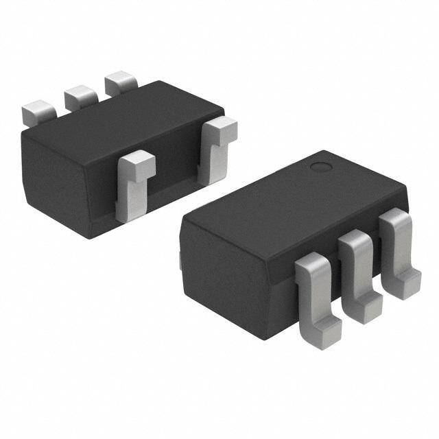
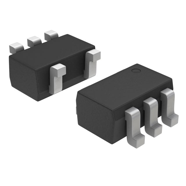
| 产品图片 |
|
| rohs | 符合RoHS无铅 / 符合限制有害物质指令(RoHS)规范要求 |
| 产品系列 | 开关 IC,模拟开关 IC,ON Semiconductor M74VHC1GT66DFT1G74VHC |
| 数据手册 | |
| 产品型号 | M74VHC1GT66DFT1G |
| 产品种类 | 模拟开关 IC |
| 供应商器件封装 | SC-70 |
| 其它名称 | M74VHC1GT66DFT1G-ND |
| 功能 | |
| 包装 | 带卷 (TR) |
| 商标 | ON Semiconductor |
| 安装类型 | 表面贴装 |
| 安装风格 | SMD/SMT |
| 导通电阻 | 40 欧姆 |
| 导通电阻—最大值 | 60 Ohms |
| 封装 | Reel |
| 封装/外壳 | 6-TSSOP(5 引线),SC-88A,SOT-353 |
| 封装/箱体 | SOT-353-5 |
| 工作温度 | -55°C ~ 125°C |
| 工作电源电压 | 3 V, 5 V |
| 工厂包装数量 | 3000 |
| 开关配置 | SPST |
| 最大功率耗散 | 150 mW |
| 最大工作温度 | + 125 C |
| 最小工作温度 | - 55 C |
| 标准包装 | 3,000 |
| 电压-电源,单/双 (±) | 2 V ~ 5.5 V |
| 电压源 | 单电源 |
| 电流-电源 | - |
| 电源电压-最大 | 5.5 V |
| 电源电压-最小 | 2 V |
| 电路 | 1 x SPST - NO |
| 空闲时间—最大值 | 40 ns |
| 系列 | MC74VHC1GT66 |
| 运行时间—最大值 | 40 ns |
| 零件号别名 | M74VHC1GT66DFT2G |


- 商务部:美国ITC正式对集成电路等产品启动337调查
- 曝三星4nm工艺存在良率问题 高通将骁龙8 Gen1或转产台积电
- 太阳诱电将投资9.5亿元在常州建新厂生产MLCC 预计2023年完工
- 英特尔发布欧洲新工厂建设计划 深化IDM 2.0 战略
- 台积电先进制程称霸业界 有大客户加持明年业绩稳了
- 达到5530亿美元!SIA预计今年全球半导体销售额将创下新高
- 英特尔拟将自动驾驶子公司Mobileye上市 估值或超500亿美元
- 三星加码芯片和SET,合并消费电子和移动部门,撤换高东真等 CEO
- 三星电子宣布重大人事变动 还合并消费电子和移动部门
- 海关总署:前11个月进口集成电路产品价值2.52万亿元 增长14.8%


PDF Datasheet 数据手册内容提取
MC74VHC1GT66 SPST (NO) Normally Open Analog Switch The MC74VHC1GT66 is a Single Pole Single Throw (SPST) analog switch. It achieves high speed propagation delays and low ON resistances while maintaining low power dissipation. This bilateral switch controls analog and digital voltages that may vary across the http://onsemi.com full power−supply range (from V to GND). CC MARKING The MC74VHC1GT66 is compatible in function to a single gate of DIAGRAMS the High Speed CMOS MC74VHCT4066 and the metal−gate CMOS MC14066. The device has been designed so that the ON resistances 5 SC−88A (RON) are much lower and more linear over input voltage than RON of 5 DF SUFFIX M VE M(cid:2) the metal−gate CMOS or High Speed CMOS analog switches. 1 CASE 419A (cid:2) The ON/OFF Control input is compatible with TTL−type input 1 thresholds allowing the device to be used as a logic−level translator from 3 V CMOS logic to 5 V CMOS logic or from 1.8 V CMOS logic to 3 V CMOS logic while operating at the high−voltage power supply. 5 TSOP−5 The input protection circuitry on this device allows overvoltage 5 VE M(cid:2) DT SUFFIX tolerance on the input, which provides protection when voltages of up (cid:2) CASE 483 1 to 7 V are applied, regardless of the supply voltage. This allows the 1 MC74VHC1GT66 to be used to interface 5 V circuits to 3 V circuits. VE = Device Code Features M = Date Code* • High Speed: t = 20 ns (Typ) at V = 5 V W = Work Week PD CC • Low Power Dissipation: I = 1.0 (cid:2)A (Max) at T = 25°C (cid:2) = Pb−Free Package CC A (Note: Microdot may be in either location) • Diode Protection Provided on Inputs and Outputs *Date Code orientation and/or position may vary • depending upon manufacturing location. Improved Linearity and Lower ON Resistance over Input Voltage • On/Off Control Input Has OVT • Chip Complexity: FETs = 11; Equivalent Gates = 3 PIN ASSIGNMENT • Pb−Free Packages are Available 1 IN/OUT XA 2 OUT/IN YA 3 GND 4 ON/OFF CONTROL 5 VCC FUNCTION TABLE On/Off Control Input State of Analog Switch L Off H On ORDERING INFORMATION See detailed ordering and shipping information in the package dimensions section on page 7 of this data sheet. © Semiconductor Components Industries, LLC, 2011 1 Publication Order Number: August, 2011 − Rev. 15 MC74VHC1GT66/D
MC74VHC1GT66 IN/OUT XA 1 5 VCC OUT/IN YA 2 GND 3 4 ON/OFF CONTROL (SC−88A, TSOP−5) Figure 1. Pinout Diagram ON/OFF CONTROL X 1 U U IN/OUT XA 1 1 OUT/IN YA Figure 2. Logic Symbol MAXIMUM RATINGS Symbol Characteristics Value Unit VCC DC Supply Voltage −0.5 to +7.0 V VIN DC Input Voltage −0.5 to +7.0 V VIS Analog Output Voltage −0.5 to 7.0 V IIK Input Diode Current −20 mA ICC DC Supply Current, VCC and GND +25 mA TSTG Storage Temperature Range (cid:2)65 to (cid:3)150 °C TL Lead Temperature, 1 mm from Case for 10 Seconds 260 °C TJ Junction Temperature Under Bias (cid:3)150 °C (cid:3)JA Thermal Resistance SC70−5 (Note 1) 350 °C/W SOT23−5 230 PD Power Dissipation in Still Air at 85°C SC70−5 150 mW SOT23−5 200 MSL Moisture Sensitivity Level 1 FR Flammability Rating Oxygen Index: 28 to 34 UL 94 V−0 @ 0.125 in VESD ESD Withstand Voltage Human Body Model (Note 2) (cid:4)2000 V Machine Model (Note 3) (cid:4)200 Charged Device Model (Note 4) N/A ILatchup Latchup Performance Above VCC and Below GND at 125°C (Note 5) (cid:5)500 mA Stresses exceeding Maximum Ratings may damage the device. Maximum Ratings are stress ratings only. Functional operation above the Recommended Operating Conditions is not implied. Extended exposure to stresses above the Recommended Operating Conditions may affect device reliability. 1. Measured with minimum pad spacing on an FR4 board, using 10 mm−by−1 inch, 2−ounce copper trace with no air flow. 2. Tested to EIA/JESD22−A114−A. 3. Tested to EIA/JESD22−A115−A. 4. Tested to JESD22−C101−A. 5. Tested to EIA/JESD78. http://onsemi.com 2
MC74VHC1GT66 RECOMMENDED OPERATING CONDITIONS Symbol Characteristics Min Max Unit VCC DC Supply Voltage 2.0 5.5 V VIN Digital Input Voltage GND 5.5 V VIS Analog Input Voltage GND VCC V TA Operating Temperature Range −55 +125 °C tr , tf Input Rise and Fall Time VCC = 3.3 V ± 0.3 V 0 100 ns/V VCC = 5.0 V ± 0.5 V 0 20 Device Junction Temperature versus Time to 0.1% Bond Failures Junction TE FAILURE RATE OF PLASTIC = CERAMIC Temperature °C Time, Hours Time, Years RA UNTIL INTERMETALLICS OCCUR E 80 1,032,200 117.8 R C C C C C C 90 419,300 47.9 FAILU °= 130 °=120 °=110 °=100 °= 90 °= 80 100 178,700 20.4 D TJ TJ TJ TJ TJ TJ E Z 1 110 79,600 9.4 LI A M 120 37,000 4.2 OR 1 10 100 1000 130 17,800 2.0 N TIME, YEARS 140 8,900 1.0 Figure 3. Failure Rate vs. Time Junction Temperature http://onsemi.com 3
MC74VHC1GT66 DC ELECTRICAL CHARACTERISTICS TA = 25°C TA ≤ 85°C −55°C ≤ TA ≤ 125°C VCC Symbol Parameter Test Conditions (V) Min Max Min Max Min Max Unit VIH Minimum High−Level RON = Per Spec V Input Voltage 3.0 1.2 1.2 1.2 ON/OFF Control Input 4.5 2.0 2.0 2.0 5.5 2.0 2.0 2.0 VIL Maximum Low−Level RON = Per Spec V Input Voltage 3.0 0.53 0.53 0.53 ON/OFF Control Input 4.5 0.8 0.8 0.8 5.5 0.8 0.8 0.8 IIN Maximum Input VIN = VCC or GND 0 to ±0.1 ±1.0 ±1.0 (cid:2)A Leakage Current 5.5 ON/OFF Control Input ICC Maximum Quiescent VIN = VCC or GND 5.5 1.0 20 40 (cid:2)A Supply Current VIO = 0 V ICCT Quiescent ON/OFF Control at 5.5 1.35 1.5 1.65 mA Supply Current 3.4 V RON Maximum ”ON” VIN = VIH 3.0 60 70 100 (cid:4) Resistance VIS = VCC or GND 4.5 45 50 60 |IIS| ≤ 10 mA (Figure 4) 5.5 40 45 55 IOFF Maximum Off−Channel VIN = VIL 5.5 0.1 0.5 1.0 (cid:2)A Leakage Current VIS = VCC or GND Switch Off (Figure 5) AC ELECTRICAL CHARACTERISTICS Cload = 50 pF, Input tr/tf = 3.0 ns TA = 25°C TA ≤ 85°C −55°C ≤ TA ≤ 125°C VCC Symbol Parameter Test Conditions (V) Min Typ Max Min Max Min Max Unit tPLH, Maximum Propagation YA = Open 2.0 1 5 6 7 ns tPHL Delay, Input X to Y 3.0 0.6 2 3 4 (Figures 7, 14) 4.5 0.6 1 1 2 5.5 0.6 1 1 1 tPLZ, Maximum Propagation RL = 1000 (cid:4) 2.0 32 40 45 50 ns tPHZ Delay, ON/OFF Control 3.0 28 35 40 45 to Analog Output (Figures 8, 15) 4.5 24 30 35 40 5.5 20 25 30 35 tPZL, Maximum Propagation RL = 1000 (cid:4) 2.0 32 40 45 50 ns tPZH Delay, ON/OFF Control 3.0 28 35 40 45 to Analog Output (Figures 8, 15) 4.5 24 30 35 40 5.5 20 25 30 35 CIN Maximum Input ON/OFF Control Input 0.0 3 10 10 10 pF Capacitance Control Input = GND 5.0 Analog I/O 4 10 10 10 Feedthrough 4 10 10 10 Typical @ 25°C, VCC = 5.0 V CPD Power Dissipation Capacitance (Note 6) 18 pF 6. CPD is defined as the value of the internal equivalent capacitance which is calculated from the operating current consumption without load. Average operating current can be obtained by the equation: ICC(OPR) = CPD (cid:2) VCC (cid:2) fin + ICC. CPD is used to determine the no−load dynamic power consumption; PD = CPD (cid:2) VCC2 (cid:2) fin + ICC (cid:2) VCC. http://onsemi.com 4
MC74VHC1GT66 ADDITIONAL APPLICATION CHARACTERISTICS (Voltages Referenced to GND Unless Noted) Symbol Parameter Test Conditions VCC Limit 25°C Unit BW Maximum On−Channel Bandwidth fin = 1 MHz Sine Wave 3.0 150 MHz or Minimum Frequency Response Adjust fin voltage to obtain 0 dBm at VOS 4.5 175 (Figure 10) Increase fin = frequency until dB meter reads −3 dB 5.5 180 RL = 50 (cid:4) ISOoff Off−Channel Feedthrough Isolation fin = Sine Wave 3.0 −80 dB (Figure 11) Adjust fin voltage to obtain 0 dBm at VIS 4.5 −80 fin = 10 kHz, RL = 600 (cid:4) 5.5 −80 NOISEfeed Feedthrough Noise Control to Vin ≤ 1 MHz Square Wave (tr = tf = 2ns) 3.0 45 mVPP Switch 4.5 60 (Figure 12) RL = 600 (cid:4) 5.5 130 THD Total Harmonic Distortion fin = 1 kHz, RL = 10 k(cid:4) % (Figure 13) THD = THDMeasured − THDSource VIS = 3.0 VPP sine wave 3.3 0.30 VIS = 5.0 VPP sine wave 5.5 0.15 PLOTTER POWER DC PARAMETER SUPPLY COMPUTER ANALYZER − + VCC VCC VCC 1 5 1 5 2 VIH 2 VIL 3 4 VCC A 3 4 Figure 4. On Resistance Test Set−Up Figure 5. Maximum Off−Channel Leakage Current Test Set−Up VCC VCC VCC A 1 5 1 5 N/C 2 VIH TEST 2 VIH POINT 3 4 3 4 Figure 6. Maximum On−Channel Leakage Current Figure 7. Propagation Delay Test Set−Up Test Set−Up http://onsemi.com 5
MC74VHC1GT66 Switch to Position 2 when testing tPLZ and tPZL Switch to Position 1 when testing tPHZ and tPZH TEST POINT VCC VCC 1 VCC A 1 5 N/C 1 5 2 RL 2 VCC 1 CL* 3 4 N/C 2 3 4 2 *Includes all probe and jig capacitance. Figure 8. Propagation Delay Output Enable/Disable Figure 9. Power Dissipation Capacitance Test Set−Up Test Set−Up VOS VIS VOS 0.1 (cid:2)F VCC 0.1 (cid:2)F VCC fin 1 5 fin 1 5 2 2 dB 3 4 dB RL 3 4 Meter Meter *Includes all probe and jig capacitance. *Includes all probe and jig capacitance. Figure 10. Maximum On−Channel Bandwidth Figure 11. Off−Channel Feedthrough Isolation Test Set−Up Test Set−Up To Distortion Meter (VCC)/2 (VCC)/2 VIS RL VCC 0.1 (cid:2)F VCC RL 1 5 RL fin 1 5 V (cid:6)1MHz VOS IN VOS IS 2 tr(cid:7)tf(cid:7)2ns 2 VIH 3 4 VIH 3 4 GND *Includes all probe and jig capacitance. *Includes all probe and jig capacitance. Figure 12. Feedthrough Noise, ON/OFF Control to Figure 13. Total Harmonic Distortion Test Set−Up Analog Out, Test Set−Up http://onsemi.com 6
MC74VHC1GT66 XA VCC 1.5 V 1.5 V tPLH tPHL VOH YA 50% VCC VOL Figure 14. Propagation Delay, Analog In to Analog Out Waveforms tr tf 90% VIH Control 1.5 V 10% tPZL tPLZ High 50% VCC 10% Impedance Analog Out VOL 90% VOH 50% VCC High tPZH tPHZ Impedance Figure 15. Propagation Delay, ON/OFF Control ORDERING INFORMATION Device Package Shipping† M74VHC1GT66DFT1G SC−88A (Pb−Free) MC74VHC1GT66DFT2 SC−88A M74VHC1GT66DFT2G SC−88A 3000 / Tape & Reel (Pb−Free) MC74VHC1GT66DTT1 TSOP−5 M74VHC1GT66DTT1G TSOP−5 (Pb−Free) †For information on tape and reel specifications, including part orientation and tape sizes, please refer to our Tape and Reel Packaging Specifications Brochure, BRD8011/D. http://onsemi.com 7
MC74VHC1GT66 PACKAGE DIMENSIONS SC−88A (SC−70−5/SOT−353) CASE 419A−02 ISSUE K A NOTES: 1. DIMENSIONING AND TOLERANCING G PER ANSI Y14.5M, 1982. 2. CONTROLLING DIMENSION: INCH. 3. 419A−01 OBSOLETE. NEW STANDARD 419A−02. 4. DIMENSIONS A AND B DO NOT INCLUDE 5 4 MOLD FLASH, PROTRUSIONS, OR GATE BURRS. S −B− INCHES MILLIMETERS 1 2 3 DIM MIN MAX MIN MAX A 0.071 0.087 1.80 2.20 B 0.045 0.053 1.15 1.35 C 0.031 0.043 0.80 1.10 D 0.004 0.012 0.10 0.30 D 5 PL 0.2 (0.008) M B M G 0.026 BSC 0.65 BSC H --- 0.004 --- 0.10 J 0.004 0.010 0.10 0.25 N K 0.004 0.012 0.10 0.30 N 0.008 REF 0.20 REF S 0.079 0.087 2.00 2.20 J C K H SOLDERING FOOTPRINT* 0.50 0.0197 0.65 0.025 0.65 0.025 0.40 0.0157 (cid:8) (cid:9) 1.9 SCALE 20:1 mm inches 0.0748 *For additional information on our Pb−Free strategy and soldering details, please download the ON Semiconductor Soldering and Mounting Techniques Reference Manual, SOLDERRM/D. http://onsemi.com 8
MC74VHC1GT66 PACKAGE DIMENSIONS TSOP−5 CASE 483−02 ISSUE H NOTES: 1. DIMENSIONING AND TOLERANCING PER NOTE 5 D5X ASME Y14.5M, 1994. 2. CONTROLLING DIMENSION: MILLIMETERS. 0.20 C A B 3. MAXIMUM LEAD THICKNESS INCLUDES 2X 0.10 T LEAD FINISH THICKNESS. MINIMUM LEAD THICKNESS IS THE MINIMUM THICKNESS M OF BASE MATERIAL. 2X 0.20 T 5 4 B S 4. DMIOMLEDN FSLIOANSSH ,A P ARNODT RBU DSOIO NNOST, OINRC GLUATDEE 1 2 3 BURRS. K 5. OPTIONAL CONSTRUCTION: AN L DETAIL Z ADDITIONAL TRIMMED LEAD IS ALLOWED G IN THIS LOCATION. TRIMMED LEAD NOT TO EXTEND MORE THAN 0.2 FROM BODY. A MILLIMETERS DIM MIN MAX DETAIL Z A 3.00 BSC J B 1.50 BSC C C 0.90 1.10 0.05 H SPELAATNIENG GD 0.02.595 BS0C.50 H 0.01 0.10 T J 0.10 0.26 K 0.20 0.60 L 1.25 1.55 M 0 (cid:3) 10 (cid:3) S 2.50 3.00 SOLDERING FOOTPRINT* 1.9 0.074 0.95 0.037 2.4 0.094 1.0 0.039 0.7 (cid:8) (cid:9) 0.028 SCALE 10:1 mm inches *For additional information on our Pb−Free strategy and soldering details, please download the ON Semiconductor Soldering and Mounting Techniques Reference Manual, SOLDERRM/D. ON Semiconductor and are registered trademarks of Semiconductor Components Industries, LLC (SCILLC). SCILLC reserves the right to make changes without further notice to any products herein. SCILLC makes no warranty, representation or guarantee regarding the suitability of its products for any particular purpose, nor does SCILLC assume any liability arising out of the application or use of any product or circuit, and specifically disclaims any and all liability, including without limitation special, consequential or incidental damages. “Typical” parameters which may be provided in SCILLC data sheets and/or specifications can and do vary in different applications and actual performance may vary over time. All operating parameters, including “Typicals” must be validated for each customer application by customer’s technical experts. SCILLC does not convey any license under its patent rights nor the rights of others. SCILLC products are not designed, intended, or authorized for use as components in systems intended for surgical implant into the body, or other applications intended to support or sustain life, or for any other application in which the failure of the SCILLC product could create a situation where personal injury or death may occur. Should Buyer purchase or use SCILLC products for any such unintended or unauthorized application, Buyer shall indemnify and hold SCILLC and its officers, employees, subsidiaries, affiliates, and distributors harmless against all claims, costs, damages, and expenses, and reasonable attorney fees arising out of, directly or indirectly, any claim of personal injury or death associated with such unintended or unauthorized use, even if such claim alleges that SCILLC was negligent regarding the design or manufacture of the part. SCILLC is an Equal Opportunity/Affirmative Action Employer. This literature is subject to all applicable copyright laws and is not for resale in any manner. PUBLICATION ORDERING INFORMATION LITERATURE FULFILLMENT: N. American Technical Support: 800−282−9855 Toll Free ON Semiconductor Website: www.onsemi.com Literature Distribution Center for ON Semiconductor USA/Canada P.O. Box 5163, Denver, Colorado 80217 USA Europe, Middle East and Africa Technical Support: Order Literature: http://www.onsemi.com/orderlit Phone: 303−675−2175 or 800−344−3860 Toll Free USA/Canada Phone: 421 33 790 2910 Fax: 303−675−2176 or 800−344−3867 Toll Free USA/Canada Japan Customer Focus Center For additional information, please contact your local Email: orderlit@onsemi.com Phone: 81−3−5773−3850 Sales Representative http://onsemi.com MC74VHC1GT66/D 9
Mouser Electronics Authorized Distributor Click to View Pricing, Inventory, Delivery & Lifecycle Information: O N Semiconductor: M74VHC1GT66DFT1G M74VHC1GT66DFT2G M74VHC1GT66DTT1G