ICGOO在线商城 > 集成电路(IC) > 逻辑 - 栅极和逆变器 > M74VHC1GT04DFT2G
 Datasheet下载
- 型号: M74VHC1GT04DFT2G
- 制造商: ON Semiconductor
- 库位|库存: xxxx|xxxx
- 要求:
| 数量阶梯 | 香港交货 | 国内含税 |
| +xxxx | $xxxx | ¥xxxx |
查看当月历史价格
查看今年历史价格
M74VHC1GT04DFT2G产品简介:
ICGOO电子元器件商城为您提供M74VHC1GT04DFT2G由ON Semiconductor设计生产,在icgoo商城现货销售,并且可以通过原厂、代理商等渠道进行代购。 M74VHC1GT04DFT2G价格参考¥询价-¥询价。ON SemiconductorM74VHC1GT04DFT2G封装/规格:逻辑 - 栅极和逆变器, Inverter IC 1 Channel SC-88A (SC-70-5/SOT-353)。您可以下载M74VHC1GT04DFT2G参考资料、Datasheet数据手册功能说明书,资料中有M74VHC1GT04DFT2G 详细功能的应用电路图电压和使用方法及教程。
M74VHC1GT04DFT2G 是一款由 ON Semiconductor(安森美半导体)生产的单通道 CMOS 反相器(逆变器),属于逻辑 - 栅极和逆变器系列。以下是其主要应用场景:

 1. 数字电路设计
   - M74VHC1GT04DFT2G 常用于数字电路中的信号反相操作,将输入信号的逻辑电平反转(高变低,低变高)。这种功能在许多数字系统中不可或缺,例如时钟信号生成、数据信号处理等。
   - 它可以与其他逻辑器件配合使用,构建更复杂的数字电路,如计数器、编码器、解码器等。

 2. 时钟信号生成与处理
   - 在需要生成或处理时钟信号的应用中,该器件可用于创建反相信号。例如,在双相时钟系统中,一个时钟信号可以通过此逆变器生成其互补信号。

 3. 驱动能力增强
   - M74VHC1GT04DFT2G 具有较高的驱动能力,适用于驱动负载较大的电路。它可以用来增强弱信号的输出能力,确保信号能够可靠地传输到后续电路。

 4. 电平转换
   - 由于其工作电压范围较宽(通常为 2V 至 6V),该器件可以用于不同电压系统的电平转换。例如,将低电压信号转换为适合更高电压电路的信号。

 5. 噪声抑制与信号整形
   - 在某些应用中,该逆变器可用于对输入信号进行整形,以消除噪声干扰并生成清晰的方波信号。这对于提高数字系统的可靠性非常重要。

 6. 消费电子与工业控制
   - 在消费电子产品(如家用电器、音频设备)和工业控制系统中,该器件常用于信号处理和逻辑控制。例如,在自动化设备中实现简单的逻辑判断或状态切换。

 7. 通信接口
   - 在通信接口电路中,M74VHC1GT04DFT2G 可用于信号反相或电平调整,以满足特定通信协议的要求。

总之,M74VHC1GT04DFT2G 是一款通用性较强的单通道 CMOS 反相器,广泛应用于各种需要信号反相、驱动增强和逻辑控制的场景中。其低功耗、高稳定性和宽工作电压范围使其成为许多数字电路设计的理想选择。
| 参数 | 数值 |
| 产品目录 | 集成电路 (IC)半导体 |
| 描述 | IC GATE INVERTER SNGL 1IN SOT353变换器 3-5.5V Single TTL |
| 产品分类 | |
| 品牌 | ON Semiconductor |
| 产品手册 | |
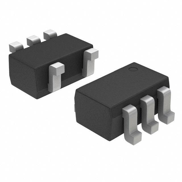
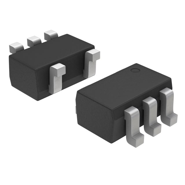
| 产品图片 |
|
| rohs | 符合RoHS无铅 / 符合限制有害物质指令(RoHS)规范要求 |
| 产品系列 | 逻辑集成电路,变换器,ON Semiconductor M74VHC1GT04DFT2G74VHC |
| 数据手册 | |
| 产品型号 | M74VHC1GT04DFT2G |
| PCN设计/规格 | |
| 不同V、最大CL时的最大传播延迟 | 7.7ns @ 5V,50pF |
| 产品种类 | 变换器 |
| 低电平输出电流 | 8 mA |
| 供应商器件封装 | SC-70 |
| 其它名称 | M74VHC1GT04DFT2GOSCT |
| 包装 | 剪切带 (CT) |
| 商标 | ON Semiconductor |
| 安装类型 | 表面贴装 |
| 安装风格 | SMD/SMT |
| 封装 | Reel |
| 封装/外壳 | 6-TSSOP(5 引线),SC-88A,SOT-353 |
| 封装/箱体 | SC-70-5 |
| 工作温度 | -55°C ~ 125°C |
| 工厂包装数量 | 3000 |
| 最大工作温度 | + 125 C |
| 标准包装 | 1 |
| 特性 | - |
| 电压-电源 | 3 V ~ 5.5 V |
| 电流-输出高,低 | 8mA,8mA |
| 电流-静态(最大值) | 1µA |
| 电源电压-最大 | 5.5 V |
| 电源电压-最小 | 3 V |
| 电路数 | 1 |
| 电路数量 | 1 Circuit |
| 系列 | MC74VHC1GT04 |
| 输入数 | 1 |
| 逻辑电平-低 | 0.53 V ~ 0.8 V |
| 逻辑电平-高 | 1.4 V ~ 2 V |
| 逻辑类型 | CMOS |
| 逻辑系列 | 74VHC |
| 零件号别名 | M74VHC1GT04DFT1G |
| 高电平输出电流 | - 8 mA |


- 商务部:美国ITC正式对集成电路等产品启动337调查
- 曝三星4nm工艺存在良率问题 高通将骁龙8 Gen1或转产台积电
- 太阳诱电将投资9.5亿元在常州建新厂生产MLCC 预计2023年完工
- 英特尔发布欧洲新工厂建设计划 深化IDM 2.0 战略
- 台积电先进制程称霸业界 有大客户加持明年业绩稳了
- 达到5530亿美元!SIA预计今年全球半导体销售额将创下新高
- 英特尔拟将自动驾驶子公司Mobileye上市 估值或超500亿美元
- 三星加码芯片和SET,合并消费电子和移动部门,撤换高东真等 CEO
- 三星电子宣布重大人事变动 还合并消费电子和移动部门
- 海关总署:前11个月进口集成电路产品价值2.52万亿元 增长14.8%


PDF Datasheet 数据手册内容提取
MC74VHC1GT04 Inverting Buffer / CMOS Logic Level Shifter LSTTL−Compatible Inputs The MC74VHC1GT04 is a single gate inverting buffer fabricated with silicon gate CMOS technology. It achieves high speed operation www.onsemi.com similar to equivalent Bipolar Schottky TTL while maintaining CMOS low power dissipation. MARKING The internal circuit is composed of three stages, including a buffer DIAGRAMS output which provides high noise immunity and stable output. The device input is compatible with TTL−type input thresholds and the output has a full 5 V CMOS level output swing. The input protection 5 SC−88A circuitry on this device allows overvoltage tolerance on the input, 5 DF SUFFIX M VK M(cid:2) allowing the device to be used as a logic−level translator from 3 V CASE 419A (cid:2) 1 CMOS logic to 5 V CMOS Logic or from 1.8 V CMOS logic to 3 V 1 CMOS Logic while operating at the high−voltage power supply. The MC74VHC1GT04 input structure provides protection when 5 voltages up to 7.0 V are applied, regardless of the supply voltage. This TSOP−5 allows the MC74VHC1GT04 to be used to interface 5 V circuits to 5 DT SUFFIX VK M (cid:2) (cid:2) 3 V circuits. The output structures also provide protection CASE 483 1 1 when V = 0 V. These input and output structures help prevent CC device destruction caused by supply voltage − input/output voltage mismatch, battery backup, hot insertion, etc. VK = Device Code M = Date Code* Features (cid:2) = Pb−Free Package • High Speed: t = 3.8 ns (Typ) at V = 5 V (Note: Microdot may be in either location) PD CC • Low Power Dissipation: I = 1 (cid:2)A (Max) at T = 25°C *Date Code orientation and/or position may vary CC A depending upon manufacturing location. • TTL−Compatible Inputs: V = 0.8 V; V = 2 V IL IH • CMOS−Compatible Outputs: V > 0.8 V ; V < 0.1 V @ Load OH CC OL CC • Power Down Protection Provided on Inputs and Outputs PIN ASSIGNMENT • Balanced Propagation Delays 1 NC • Pin and Function Compatible with Other Standard Logic Families 2 IN A • 3 GND Chip Complexity: FETs = 105; Equivalent Gates = 26 • NLV Prefix for Automotive and Other Applications Requiring 4 OUT Y Unique Site and Control Change Requirements; AEC−Q100 5 VCC Qualified and PPAP Capable • These Devices are Pb−Free, Halogen Free/BFR Free and are RoHS Compliant FUNCTION TABLE A Input Y Output NC 1 5 VCC L H H L IN A 2 GND 3 4 OUT Y ORDERING INFORMATION Figure 1. Pinout (Top View) See detailed ordering and shipping information in the package dimensions section on page 4 of this data sheet. 1 IN A OUT Y Figure 2. Logic Symbol © Semiconductor Components Industries, LLC, 2016 1 Publication Order Number: July, 2016 − Rev. 18 MC74VHC1GT04/D
MC74VHC1GT04 MAXIMUM RATINGS Symbol Characteristics Value Unit VCC DC Supply Voltage −0.5 to +7.0 V VIN DC Input Voltage −0.5 to +7.0 V VOUT DC Output Voltage VCC = 0 −0.5 to 7.0 V High or Low State −0.5 to VCC + 0.5 IIK Input Diode Current −20 mA IOK Output Diode Current VOUT < GND; VOUT > VCC +20 mA IOUT DC Output Current, per Pin +25 mA ICC DC Supply Current, VCC and GND +50 mA PD Power dissipation in still air SC−88A, TSOP−5 200 mW (cid:3)JA Thermal resistance SC−88A, TSOP−5 333 (cid:3)C/W TL Lead temperature, 1 mm from case for 10 s 260 °C TJ Junction temperature under bias +150 °C Tstg Storage temperature −65 to +150 °C VESD ESD Withstand Voltage Human Body Model (Note 1) 2000 V Machine Model (Note 2) 200 Charged Device Model (Note 3) N/A ILatchup Latchup Performance Above VCC and Below GND at 125°C (Note 4) ±100 mA Stresses exceeding those listed in the Maximum Ratings table may damage the device. If any of these limits are exceeded, device functionality should not be assumed, damage may occur and reliability may be affected. 1. Tested to EIA/JESD22−A114−A 2. Tested to EIA/JESD22−A115−A 3. Tested to JESD22−C101−A 4. Tested to EIA/JESD78 RECOMMENDED OPERATING CONDITIONS Symbol Characteristics Min Max Unit VCC DC Supply Voltage 3.0 5.5 V VIN DC Input Voltage 0.0 5.5 V VOUT DC Output Voltage VCC = 0 0.0 5.5 V High or Low State 0.0 VCC TA Operating Temperature Range −55 +125 °C tr , tf Input Rise and Fall Time VCC = 3.3 V ± 0.3 V 0 100 ns/V VCC = 5.0 V ± 0.5 V 0 20 Functional operation above the stresses listed in the Recommended Operating Ranges is not implied. Extended exposure to stresses beyond the Recommended Operating Ranges limits may affect device reliability. DEVICE JUNCTION TEMPERATURE VERSUS TIME TO 0.1% BOND FAILURES Junction E FAILURE RATE OF PLASTIC = CERAMIC T Temperature °C Time, Hours Time, Years RA UNTIL INTERMETALLICS OCCUR E 8900 14,01392,3,20000 14177..98 D FAILUR °= 130C °= 120C °= 110C °= 100C °= 90C °= 80C 100 178,700 20.4 ZE TJ TJ TJ TJ TJ TJ LI 110 79,600 9.4 MA 1 R O 120 37,000 4.2 N 1 10 100 1000 130 17,800 2.0 TIME, YEARS 140 8,900 1.0 Figure 3. Failure Rate vs. Time Junction Temperature www.onsemi.com 2
MC74VHC1GT04 DC ELECTRICAL CHARACTERISTICS TA = 25°C TA ≤ 85°C −55 ≤ TA ≤ 125°C VCC Symbol Parameter Test Conditions (V) Min Typ Max Min Max Min Max Unit VIH Minimum High−Level 3.0 1.4 1.4 1.4 V Input Voltage 4.5 2.0 2.0 2.0 5.5 2.0 2.0 2.0 VIL Maximum Low−Level 3.0 0.53 0.53 0.53 V Input Voltage 4.5 0.8 0.8 0.8 5.5 0.8 0.8 0.8 VOH Minimum High−Level VIN = VIH or VIL 3.0 2.9 3.0 2.9 2.9 V Output Voltage IOH = −50 (cid:2)A 4.5 4.4 4.5 4.4 4.4 VIN = VIH or VIL VIN = VIH or VIL V IOH = −4 mA 3.0 2.58 2.48 2.34 IOH = −8 mA 4.5 3.94 3.80 3.66 VOL Maximum Low−Level VIN = VIH or VIL 3.0 0.0 0.1 0.1 0.1 V Output Voltage IOL = 50 (cid:2)A 4.5 0.0 0.1 0.1 0.1 VIN = VIH or VIL VIN = VIH or VIL V IOL = 4.0 mA 3.0 0.36 0.44 0.52 IOL = 8.0 mA 4.5 0.36 0.44 0.52 IIN Maximum Input VIN = 5.5 V or GND 0 to ±0.1 ±1.0 ±1.0 (cid:2)A Leakage Current 5.5 ICC Maximum Quiescent VIN = VCC or GND 5.5 1.0 20 40 (cid:2)A Supply Current ICCT Quiescent Supply Input: VIN = 3.4 V 5.5 1.35 1.50 1.65 mA Current IOPD Output Leakage VOUT = 5.5 V 0.0 0.5 5.0 10 (cid:2)A Current Product parametric performance is indicated in the Electrical Characteristics for the listed test conditions, unless otherwise noted. Product performance may not be indicated by the Electrical Characteristics if operated under different conditions. AC ELECTRICAL CHARACTERISTICS Cload = 50 pF, Input tr = tf = 3.0 ns TA = 25°C TA ≤ 85°C −55 ≤ TA ≤ 125°C Symbol Parameter Test Conditions Min Typ Max Min Max Min Max Unit tPLH, Maximum Propagation VCC = 3.3 ± 0.3 V CL = 15 pF 5.0 10.0 11.0 13.0 ns tPHL Delay, Input A to Y CL = 50 pF 6.2 13.5 15.0 17.5 VCC = 5.0 ± 0.5 V CL = 15 pF 3.8 6.7 7.5 8.5 CL = 50 pF 4.2 7.7 8.5 9.5 CIN Maximum Input 5.0 10 10 10 pF Capacitance Typical @ 25°C, VCC = 5.0 V CPD Power Dissipation Capacitance (Note 5) 10 pF 5. CPD is defined as the value of the internal equivalent capacitance which is calculated from the operating current consumption without load. Average operating current can be obtained by the equation: ICC(OPR) = CPD (cid:2) VCC (cid:2) fin + ICC. CPD is used to determine the no−load dynamic power consumption; PD = CPD (cid:2) VCC2 (cid:2) fin + ICC (cid:2) VCC. www.onsemi.com 3
MC74VHC1GT04 3.0 V A 50% GND tPLH tPHL VOH Y 50% VCC VOL Figure 4. Switching Waveforms TEST POINT OUTPUT DEVICE UNDER TEST CL* *Includes all probe and jig capacitance Figure 5. Test Circuit ORDERING INFORMATION Device Package Type Package† M74VHC1GT04DFT1G NLVVHC1GT04DFT1G* SC−88A M74VHC1GT04DFT2G (Pb−Free) NLVVHC1GT04DFT2G* 3000 / Tape & Reel M74VHC1GT04DFT3G M74VHC1GT04DTT1G TSOP−5 (Pb−Free) NLVVHC1GT04DTT1G* †For information on tape and reel specifications, including part orientation and tape sizes, please refer to our Tape and Reel Packaging Specifications Brochure, BRD8011/D. *NLV Prefix for Automotive and Other Applications Requiring Unique Site and Control Change Requirements; AEC−Q100 Qualified and PPAP Capable. www.onsemi.com 4
MC74VHC1GT04 PACKAGE DIMENSIONS SC−88A (SC−70−5/SOT−353) CASE 419A−02 ISSUE L A NOTES: 1. DIMENSIONING AND TOLERANCING G PER ANSI Y14.5M, 1982. 2. CONTROLLING DIMENSION: INCH. 3. 419A−01 OBSOLETE. NEW STANDARD 419A−02. 4. DIMENSIONS A AND B DO NOT INCLUDE 5 4 MOLD FLASH, PROTRUSIONS, OR GATE BURRS. S −B− INCHES MILLIMETERS 1 2 3 DIM MIN MAX MIN MAX A 0.071 0.087 1.80 2.20 B 0.045 0.053 1.15 1.35 C 0.031 0.043 0.80 1.10 D 0.004 0.012 0.10 0.30 D 5 PL 0.2 (0.008) M B M G 0.026 BSC 0.65 BSC H --- 0.004 --- 0.10 J 0.004 0.010 0.10 0.25 N K 0.004 0.012 0.10 0.30 N 0.008 REF 0.20 REF S 0.079 0.087 2.00 2.20 J C K H SOLDER FOOTPRINT 0.50 0.0197 0.65 0.025 0.65 0.025 0.40 0.0157 1.9 (cid:2) (cid:3) 0.0748 mm SCALE 20:1 inches www.onsemi.com 5
MC74VHC1GT04 PACKAGE DIMENSIONS TSOP−5 CASE 483 ISSUE M NOTES: 1. DIMENSIONING AND TOLERANCING PER ASME NOTE 5 D5X Y14.5M, 1994. 2. CONTROLLING DIMENSION: MILLIMETERS. 0.20 C A B 3. MAXIMUM LEAD THICKNESS INCLUDES LEAD FINISH 2X 0.10 T THICKNESS. MINIMUM LEAD THICKNESS IS THE MINIMUM THICKNESS OF BASE MATERIAL. M 4. DIMENSIONS A AND B DO NOT INCLUDE MOLD 2X 0.20 T B 5 4 S FFLLAASSHH,, PPRROOTTRRUUSSIIOONNSS,, OORR GGAATTEE BBUURRRRSS. SMHOALLDL NOT 1 2 3 EXCEED 0.15 PER SIDE. DIMENSION A. K 5. OPTIONAL CONSTRUCTION: AN ADDITIONAL B G DETAIL Z TTRRIIMMMMEEDD LLEEAADD INSO ATL TLOO WEXETDE INND T HMIOS RLEO CTHATAINO N0..2 A A FROM BODY. MILLIMETERS TOP VIEW DIM MIN MAX A 2.85 3.15 B 1.35 1.65 DETAIL Z C 0.90 1.10 J D 0.25 0.50 C G 0.95 BSC H 0.01 0.10 0.05 J 0.10 0.26 H C SPELAATNIENG END VIEW MK 0.02 0(cid:3) 010.6 (cid:3) 0 SIDE VIEW S 2.50 3.00 SOLDERING FOOTPRINT* 1.9 0.074 0.95 0.037 2.4 0.094 1.0 0.039 0.7 (cid:2) (cid:3) 0.028 SCALE 10:1 mm inches *For additional information on our Pb−Free strategy and soldering details, please download the ON Semiconductor Soldering and Mounting Techniques Reference Manual, SOLDERRM/D. ON Semiconductor and are trademarks of Semiconductor Components Industries, LLC dba ON Semiconductor or its subsidiaries in the United States and/or other countries. ON Semiconductor owns the rights to a number of patents, trademarks, copyrights, trade secrets, and other intellectual property. A listing of ON Semiconductor’s product/patent coverage may be accessed at www.onsemi.com/site/pdf/Patent−Marking.pdf. ON Semiconductor reserves the right to make changes without further notice to any products herein. ON Semiconductor makes no warranty, representation or guarantee regarding the suitability of its products for any particular purpose, nor does ON Semiconductor assume any liability arising out of the application or use of any product or circuit, and specifically disclaims any and all liability, including without limitation special, consequential or incidental damages. Buyer is responsible for its products and applications using ON Semiconductor products, including compliance with all laws, regulations and safety requirements or standards, regardless of any support or applications information provided by ON Semiconductor. “Typical” parameters which may be provided in ON Semiconductor data sheets and/or specifications can and do vary in different applications and actual performance may vary over time. All operating parameters, including “Typicals” must be validated for each customer application by customer’s technical experts. ON Semiconductor does not convey any license under its patent rights nor the rights of others. ON Semiconductor products are not designed, intended, or authorized for use as a critical component in life support systems or any FDA Class 3 medical devices or medical devices with a same or similar classification in a foreign jurisdiction or any devices intended for implantation in the human body. Should Buyer purchase or use ON Semiconductor products for any such unintended or unauthorized application, Buyer shall indemnify and hold ON Semiconductor and its officers, employees, subsidiaries, affiliates, and distributors harmless against all claims, costs, damages, and expenses, and reasonable attorney fees arising out of, directly or indirectly, any claim of personal injury or death associated with such unintended or unauthorized use, even if such claim alleges that ON Semiconductor was negligent regarding the design or manufacture of the part. ON Semiconductor is an Equal Opportunity/Affirmative Action Employer. This literature is subject to all applicable copyright laws and is not for resale in any manner. PUBLICATION ORDERING INFORMATION LITERATURE FULFILLMENT: N. American Technical Support: 800−282−9855 Toll Free ON Semiconductor Website: www.onsemi.com Literature Distribution Center for ON Semiconductor USA/Canada 19521 E. 32nd Pkwy, Aurora, Colorado 80011 USA Europe, Middle East and Africa Technical Support: Order Literature: http://www.onsemi.com/orderlit Phone: 303−675−2175 or 800−344−3860 Toll Free USA/Canada Phone: 421 33 790 2910 Fax: 303−675−2176 or 800−344−3867 Toll Free USA/Canada Japan Customer Focus Center For additional information, please contact your local Email: orderlit@onsemi.com Phone: 81−3−5817−1050 Sales Representative www.onsemi.com MC74VHC1GT04/D 6
Mouser Electronics Authorized Distributor Click to View Pricing, Inventory, Delivery & Lifecycle Information: O N Semiconductor: M74VHC1GT04DFT1G M74VHC1GT04DFT2G M74VHC1GT04DTT1G NLVVHC1GT04DFT1G NLVVHC1GT04DFT2G