ICGOO在线商城 > 集成电路(IC) > 时钟/计时 - 实时时钟 > M41T93ZMY6F
 Datasheet下载
- 型号: M41T93ZMY6F
- 制造商: STMicroelectronics
- 库位|库存: xxxx|xxxx
- 要求:
| 数量阶梯 | 香港交货 | 国内含税 |
| +xxxx | $xxxx | ¥xxxx |
查看当月历史价格
查看今年历史价格
M41T93ZMY6F产品简介:
ICGOO电子元器件商城为您提供M41T93ZMY6F由STMicroelectronics设计生产,在icgoo商城现货销售,并且可以通过原厂、代理商等渠道进行代购。 M41T93ZMY6F价格参考。STMicroelectronicsM41T93ZMY6F封装/规格:时钟/计时 - 实时时钟, Real Time Clock (RTC) IC Clock/Calendar 7B SPI 18-SOX, 18-SOIC with Crystal (7.5mm Width)。您可以下载M41T93ZMY6F参考资料、Datasheet数据手册功能说明书,资料中有M41T93ZMY6F 详细功能的应用电路图电压和使用方法及教程。
STMicroelectronics(意法半导体)的M41T93ZMY6F是一款实时时钟(RTC)芯片,属于时钟/计时类器件。该芯片内置晶振、电池切换电路和I²C通信接口,具备年、月、日、时、分、秒的精确计时功能,并支持闰年补偿,工作温度范围宽,可靠性高。

M41T93ZMY6F主要应用于对时间记录和系统时序控制要求较高的嵌入式系统和工业设备中。典型应用场景包括:工业控制系统(如PLC、HMI),用于记录事件发生时间或定时操作;智能电表、水表、气表等公用事业计量设备,实现数据的时间戳记录;医疗设备中用于记录患者治疗或检测时间;通信设备中的时间同步模块;以及需要低功耗长时间运行的便携式设备。

该芯片支持外部电池备份,在主电源断电时仍可维持时钟运行,确保时间不丢失,适合需要持续计时的场合。其封装小巧(如SO-8窄体),便于集成在空间受限的电路板上。结合其高精度和抗干扰能力,M41T93ZMY6F广泛适用于工业、医疗、能源和通信等领域中对可靠性和稳定性要求较高的实时时间管理应用。
| 参数 | 数值 |
| 产品目录 | 集成电路 (IC)半导体 |
| 描述 | IC RTC CLK/CALENDAR SPI 18-SOX实时时钟 Serial SPI bus RTC |
| 产品分类 | |
| 品牌 | STMicroelectronics |
| 产品手册 | |
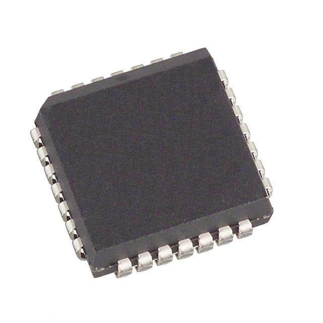
| 产品图片 |
|
| rohs | 符合RoHS无铅 / 符合限制有害物质指令(RoHS)规范要求 |
| 产品系列 | 时钟和计时器IC,实时时钟,STMicroelectronics M41T93ZMY6F- |
| 数据手册 | |
| 产品型号 | M41T93ZMY6F |
| RTC存储容量 | 32 B |
| RTC总线接口 | SPI |
| 产品培训模块 | http://www.digikey.cn/PTM/IndividualPTM.page?site=cn&lang=zhs&ptm=30015 |
| 产品目录页面 | |
| 产品种类 | |
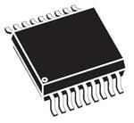
| 供应商器件封装 | 18-SOX |
| 其它名称 | 497-6891-1 |
| 其它有关文件 | http://www.st.com/web/catalog/sense_power/FM151/CL1410/SC403/PF130173?referrer=70071840 |
| 功能 | Clock, Calendar, Alarm, Interrupt |
| 包装 | 剪切带 (CT) |
| 商标 | STMicroelectronics |
| 存储容量 | 7B |
| 安装类型 | 表面贴装 |
| 安装风格 | SMD/SMT |
| 封装 | Reel |
| 封装/外壳 | 18-SOX,带晶体的 18-SOIC(7.5mm 宽) |
| 封装/箱体 | SOX-18 |
| 工作温度 | -40°C ~ 85°C |
| 工厂包装数量 | 1000 |
| 接口 | SPI |
| 日期格式 | YY-MM-DD-dd |
| 时间格式 | HH:MM:SS:hh(24 小时) |
| 最大工作温度 | + 85 C |
| 最小工作温度 | - 40 C |
| 标准包装 | 1 |
| 特性 | 警报器,闰年,方波输出,SRAM,监视计时器 |
| 电压-电源 | 2.38 V ~ 5.5 V |
| 电压-电源,电池 | 1.8 V ~ 5.5 V |
| 电池备用开关 | Yes |
| 电流-计时(最大) | 10µA @ 5.5V |
| 电源电压-最大 | 5.5 V |
| 电源电压-最小 | 2.38 V |
| 类型 | 时钟/日历 |
| 系列 | M41T93 |


- 商务部:美国ITC正式对集成电路等产品启动337调查
- 曝三星4nm工艺存在良率问题 高通将骁龙8 Gen1或转产台积电
- 太阳诱电将投资9.5亿元在常州建新厂生产MLCC 预计2023年完工
- 英特尔发布欧洲新工厂建设计划 深化IDM 2.0 战略
- 台积电先进制程称霸业界 有大客户加持明年业绩稳了
- 达到5530亿美元!SIA预计今年全球半导体销售额将创下新高
- 英特尔拟将自动驾驶子公司Mobileye上市 估值或超500亿美元
- 三星加码芯片和SET,合并消费电子和移动部门,撤换高东真等 CEO
- 三星电子宣布重大人事变动 还合并消费电子和移动部门
- 海关总署:前11个月进口集成电路产品价值2.52万亿元 增长14.8%


PDF Datasheet 数据手册内容提取
M41T93 Serial SPI bus real-time clock (RTC) with battery switchover Datasheet - production data Programmable 8-bit counter/timer 7 bytes of battery-backed user SRAM Battery low flag Low operating current of 80 μA QFN16, 4 mm x 4 mm Oscillator stop detection Battery or supercapacitor backup 18 Operating temperature of –40 °C to +85 °C 1 Package options include a 16-lead QFN and an 18-lead embedded crystal SOIC SOX18, 11.61 x 7.62 mm (embedded crystal) Features Ultra-low battery supply current of 365 nA Factory calibrated accuracy ±5 ppm typical after 2 reflows (SOX18) (much better accuracies are achievable using built-in programmable analog and digital calibration circuits) 2.0 V to 5.5 V clock operating voltage Counters for tenths/hundredths of seconds, seconds, minutes, hours, day, date, month, year, and century Automatic switchover and reset output circuitry (fixed reference): M41T93S: V = 3.0 V to 5.5 V; CC M41T93R: V = 2.7 V to 5.5 V; CC M41T93Z: V = 2.38 V to 5.50 V CC Compatible with SPI bus serial interface (supports SPI mode 0 [CPOL = 0, CPHA = 0]) Programmable alarm with interrupt function (valid even during battery backup mode) Optional 2nd programmable alarm available Square wave output (defaults to 32 KHz on power-up) RESET (RST) output Watchdog timer November 2013 DocID12615 Rev 8 1/56 This is information on a product in full production. www.st.com
Contents M41T93 Contents 1 Description . . . . . . . . . . . . . . . . . . . . . . . . . . . . . . . . . . . . . . . . . . . . . . . . 6 1.1 SPI signal description . . . . . . . . . . . . . . . . . . . . . . . . . . . . . . . . . . . . . . . . 11 1.1.1 Serial data output (SDO) . . . . . . . . . . . . . . . . . . . . . . . . . . . . . . . . . . . . 11 1.1.2 Serial data input (SDI) . . . . . . . . . . . . . . . . . . . . . . . . . . . . . . . . . . . . . . 11 1.1.3 Serial clock (SCL) . . . . . . . . . . . . . . . . . . . . . . . . . . . . . . . . . . . . . . . . . 11 1.1.4 Chip enable (E) . . . . . . . . . . . . . . . . . . . . . . . . . . . . . . . . . . . . . . . . . . . 11 2 Operation . . . . . . . . . . . . . . . . . . . . . . . . . . . . . . . . . . . . . . . . . . . . . . . . . 12 2.1 SPI bus characteristics . . . . . . . . . . . . . . . . . . . . . . . . . . . . . . . . . . . . . . . 12 2.2 READ and WRITE cycles . . . . . . . . . . . . . . . . . . . . . . . . . . . . . . . . . . . . . 13 2.3 Data retention and battery switchover (V = V ) . . . . . . . . . . . . . . . . 15 SO RST 2.4 Power-on reset (t ) . . . . . . . . . . . . . . . . . . . . . . . . . . . . . . . . . . . . . . . . . 15 rec 3 Clock operation . . . . . . . . . . . . . . . . . . . . . . . . . . . . . . . . . . . . . . . . . . . . 16 3.1 Clock data coherency . . . . . . . . . . . . . . . . . . . . . . . . . . . . . . . . . . . . . . . . 17 3.1.1 Example of incoherency . . . . . . . . . . . . . . . . . . . . . . . . . . . . . . . . . . . .17 3.1.2 Accessing the device . . . . . . . . . . . . . . . . . . . . . . . . . . . . . . . . . . . . . . .18 3.2 Halt bit (HT) operation . . . . . . . . . . . . . . . . . . . . . . . . . . . . . . . . . . . . . . . 18 3.2.1 Power-down time stamp . . . . . . . . . . . . . . . . . . . . . . . . . . . . . . . . . . . .19 3.3 Real-time clock accuracy . . . . . . . . . . . . . . . . . . . . . . . . . . . . . . . . . . . . . 21 3.4 Clock calibration . . . . . . . . . . . . . . . . . . . . . . . . . . . . . . . . . . . . . . . . . . . . 22 3.4.1 Digital calibration (periodic counter correction) . . . . . . . . . . . . . . . . . . .22 3.4.2 Analog calibration (programmable load capacitance) . . . . . . . . . . . . . .25 3.4.3 Pre-programmed calibration value . . . . . . . . . . . . . . . . . . . . . . . . . . . . .26 3.5 Setting the alarm clock registers . . . . . . . . . . . . . . . . . . . . . . . . . . . . . . . 30 3.6 Optional second programmable alarm . . . . . . . . . . . . . . . . . . . . . . . . . . . 31 3.7 Watchdog timer . . . . . . . . . . . . . . . . . . . . . . . . . . . . . . . . . . . . . . . . . . . . 31 3.8 8-bit (countdown) timer . . . . . . . . . . . . . . . . . . . . . . . . . . . . . . . . . . . . . . . 32 3.8.1 Timer interrupt/output . . . . . . . . . . . . . . . . . . . . . . . . . . . . . . . . . . . . . . .32 3.8.2 Timer flag (TF) . . . . . . . . . . . . . . . . . . . . . . . . . . . . . . . . . . . . . . . . . . . .34 3.8.3 Timer interrupt enable (TIE) . . . . . . . . . . . . . . . . . . . . . . . . . . . . . . . . . .34 3.8.4 Timer enable (TE) . . . . . . . . . . . . . . . . . . . . . . . . . . . . . . . . . . . . . . . . .34 3.8.5 TD1/0 . . . . . . . . . . . . . . . . . . . . . . . . . . . . . . . . . . . . . . . . . . . . . . . . . . .34 2/56 DocID12615 Rev 8
M41T93 Contents 3.9 Square wave output . . . . . . . . . . . . . . . . . . . . . . . . . . . . . . . . . . . . . . . . . 35 3.10 Battery low warning . . . . . . . . . . . . . . . . . . . . . . . . . . . . . . . . . . . . . . . . . 36 3.11 Century bits . . . . . . . . . . . . . . . . . . . . . . . . . . . . . . . . . . . . . . . . . . . . . . . 37 3.12 Oscillator fail detection . . . . . . . . . . . . . . . . . . . . . . . . . . . . . . . . . . . . . . . 38 3.13 Oscillator fail interrupt enable . . . . . . . . . . . . . . . . . . . . . . . . . . . . . . . . . . 38 3.14 IRQ/FT/OUT pin, frequency test, interrupts and the OUT bit . . . . . . . . . . 38 3.14.1 Active mode operation on V CC . . . . . . . . . . . . . . . . . . . . . . . . . . . . . . . . . . . . . . . . .40 3.14.2 Backup mode . . . . . . . . . . . . . . . . . . . . . . . . . . . . . . . . . . . . . . . . . . . . .41 3.15 Initial power-on defaults . . . . . . . . . . . . . . . . . . . . . . . . . . . . . . . . . . . . . . 42 3.16 OTP bit operation (SOX18 package only) . . . . . . . . . . . . . . . . . . . . . . . . 42 4 Maximum ratings . . . . . . . . . . . . . . . . . . . . . . . . . . . . . . . . . . . . . . . . . . . 43 5 DC and AC parameters . . . . . . . . . . . . . . . . . . . . . . . . . . . . . . . . . . . . . . 44 6 Package mechanical data . . . . . . . . . . . . . . . . . . . . . . . . . . . . . . . . . . . . 50 7 Part numbering . . . . . . . . . . . . . . . . . . . . . . . . . . . . . . . . . . . . . . . . . . . . 54 8 Revision history . . . . . . . . . . . . . . . . . . . . . . . . . . . . . . . . . . . . . . . . . . . 55 DocID12615 Rev 8 3/56 56
List of tables M41T93 List of tables Table 1. Signal names . . . . . . . . . . . . . . . . . . . . . . . . . . . . . . . . . . . . . . . . . . . . . . . . . . . . . . . . . . . .7 Table 2. Function table. . . . . . . . . . . . . . . . . . . . . . . . . . . . . . . . . . . . . . . . . . . . . . . . . . . . . . . . . . .10 Table 3. Clock/control register map (32 bytes). . . . . . . . . . . . . . . . . . . . . . . . . . . . . . . . . . . . . . . . .20 Table 4. Digital calibration values. . . . . . . . . . . . . . . . . . . . . . . . . . . . . . . . . . . . . . . . . . . . . . . . . . .24 Table 5. Analog calibration values . . . . . . . . . . . . . . . . . . . . . . . . . . . . . . . . . . . . . . . . . . . . . . . . . .26 Table 6. Alarm repeat modes . . . . . . . . . . . . . . . . . . . . . . . . . . . . . . . . . . . . . . . . . . . . . . . . . . . . . .31 Table 7. Timer control register map . . . . . . . . . . . . . . . . . . . . . . . . . . . . . . . . . . . . . . . . . . . . . . . . .33 Table 8. Timer interrupt operation in free-running mode (with TI/TP = 1). . . . . . . . . . . . . . . . . . . . .33 Table 9. Timer source clock frequency selection (244.1 μs to 4.25 hrs) . . . . . . . . . . . . . . . . . . . . .34 Table 10. Square wave output frequency. . . . . . . . . . . . . . . . . . . . . . . . . . . . . . . . . . . . . . . . . . . . . .35 Table 11. Priority for IRQ/FT/OUT pin when operating on V . . . . . . . . . . . . . . . . . . . . . . . . . . . . .40 CC Table 12. Priority for IRQ/FT/OUT pin when operating in backup mode . . . . . . . . . . . . . . . . . . . . . .41 Table 13. Initial power-on default values (part 1) . . . . . . . . . . . . . . . . . . . . . . . . . . . . . . . . . . . . . . . .42 Table 14. Initial power-up default values (part 2) . . . . . . . . . . . . . . . . . . . . . . . . . . . . . . . . . . . . . . . .42 Table 15. Absolute maximum ratings . . . . . . . . . . . . . . . . . . . . . . . . . . . . . . . . . . . . . . . . . . . . . . . . .43 Table 16. Operating and AC measurement conditions. . . . . . . . . . . . . . . . . . . . . . . . . . . . . . . . . . . .44 Table 17. Capacitance . . . . . . . . . . . . . . . . . . . . . . . . . . . . . . . . . . . . . . . . . . . . . . . . . . . . . . . . . . . .44 Table 18. DC characteristics. . . . . . . . . . . . . . . . . . . . . . . . . . . . . . . . . . . . . . . . . . . . . . . . . . . . . . . .45 Table 19. Crystal electrical characteristics . . . . . . . . . . . . . . . . . . . . . . . . . . . . . . . . . . . . . . . . . . . . .46 Table 20. Oscillator characteristics. . . . . . . . . . . . . . . . . . . . . . . . . . . . . . . . . . . . . . . . . . . . . . . . . . .46 Table 21. Power down/up trip points DC characteristics . . . . . . . . . . . . . . . . . . . . . . . . . . . . . . . . . .47 Table 22. AC characteristics. . . . . . . . . . . . . . . . . . . . . . . . . . . . . . . . . . . . . . . . . . . . . . . . . . . . . . . .49 Table 23. QFN16 – 16-lead, quad, flat package, no lead, 4 x 4 mm body, mech. data . . . . . . . . . . .51 Table 24. SOX18 – 18-lead plastic SO, 300 mils, embedded crystal, pkg. mech. data . . . . . . . . . . .53 Table 25. Ordering information. . . . . . . . . . . . . . . . . . . . . . . . . . . . . . . . . . . . . . . . . . . . . . . . . . . . . .54 Table 26. Document revision history. . . . . . . . . . . . . . . . . . . . . . . . . . . . . . . . . . . . . . . . . . . . . . . . . .55 4/56 DocID12615 Rev 8
M41T93 List of figures List of figures Figure 1. Logic diagram. . . . . . . . . . . . . . . . . . . . . . . . . . . . . . . . . . . . . . . . . . . . . . . . . . . . . . . . . . . .7 Figure 2. QFN16 connections . . . . . . . . . . . . . . . . . . . . . . . . . . . . . . . . . . . . . . . . . . . . . . . . . . . . . . .8 Figure 3. SOX18 connections . . . . . . . . . . . . . . . . . . . . . . . . . . . . . . . . . . . . . . . . . . . . . . . . . . . . . . .8 Figure 4. Block diagram. . . . . . . . . . . . . . . . . . . . . . . . . . . . . . . . . . . . . . . . . . . . . . . . . . . . . . . . . . . .9 Figure 5. Hardware hookup . . . . . . . . . . . . . . . . . . . . . . . . . . . . . . . . . . . . . . . . . . . . . . . . . . . . . . . .10 Figure 6. Data and clock timing . . . . . . . . . . . . . . . . . . . . . . . . . . . . . . . . . . . . . . . . . . . . . . . . . . . . .10 Figure 7. READ mode sequence. . . . . . . . . . . . . . . . . . . . . . . . . . . . . . . . . . . . . . . . . . . . . . . . . . . .14 Figure 8. WRITE mode sequence . . . . . . . . . . . . . . . . . . . . . . . . . . . . . . . . . . . . . . . . . . . . . . . . . . .14 Figure 9. Clock data coherency. . . . . . . . . . . . . . . . . . . . . . . . . . . . . . . . . . . . . . . . . . . . . . . . . . . . .17 Figure 10. Internal load capacitance adjustment. . . . . . . . . . . . . . . . . . . . . . . . . . . . . . . . . . . . . . . . .21 Figure 11. Crystal accuracy across temperature. . . . . . . . . . . . . . . . . . . . . . . . . . . . . . . . . . . . . . . . .26 Figure 12. Clock accuracy vs. on-chip load capacitors . . . . . . . . . . . . . . . . . . . . . . . . . . . . . . . . . . . .28 Figure 13. Clock divider chain and calibration circuits. . . . . . . . . . . . . . . . . . . . . . . . . . . . . . . . . . . . .29 Figure 14. Crystal isolation example . . . . . . . . . . . . . . . . . . . . . . . . . . . . . . . . . . . . . . . . . . . . . . . . . .30 Figure 15. Backup mode alarm waveform. . . . . . . . . . . . . . . . . . . . . . . . . . . . . . . . . . . . . . . . . . . . . .31 Figure 16. Timer output waveform in free-running mode (with TI/TP = 1). . . . . . . . . . . . . . . . . . . . . .33 Figure 17. Battery check . . . . . . . . . . . . . . . . . . . . . . . . . . . . . . . . . . . . . . . . . . . . . . . . . . . . . . . . . . .36 Figure 18. Two-bit binary counter (century bits CB1:CB0). . . . . . . . . . . . . . . . . . . . . . . . . . . . . . . . . .37 Figure 19. IRQ/FT/OUT output pin circuit . . . . . . . . . . . . . . . . . . . . . . . . . . . . . . . . . . . . . . . . . . . . . .39 Figure 20. Measurement AC I/O waveform . . . . . . . . . . . . . . . . . . . . . . . . . . . . . . . . . . . . . . . . . . . . .44 Figure 21. I vs. temperature. . . . . . . . . . . . . . . . . . . . . . . . . . . . . . . . . . . . . . . . . . . . . . . . . . . . . .46 CC2 Figure 22. Power down/up mode AC waveforms. . . . . . . . . . . . . . . . . . . . . . . . . . . . . . . . . . . . . . . . .47 Figure 23. Input timing requirements. . . . . . . . . . . . . . . . . . . . . . . . . . . . . . . . . . . . . . . . . . . . . . . . . .48 Figure 24. Output timing requirements. . . . . . . . . . . . . . . . . . . . . . . . . . . . . . . . . . . . . . . . . . . . . . . . .48 Figure 25. QFN16 – 16-lead, quad, flat package, no lead, 4 x 4 mm body size, outline . . . . . . . . . . .51 Figure 26. QFN16 – 16-lead, quad, flat, no lead, 4 x 4 mm, recommended footprint . . . . . . . . . . . . .52 Figure 27. 32 KHz crystal + QFN16 vs. VSOJ20 mechanical data . . . . . . . . . . . . . . . . . . . . . . . . . . .52 Figure 28. SOX18 – 18-lead plastic small outline, 300 mils, embedded crystal . . . . . . . . . . . . . . . . .53 DocID12615 Rev 8 5/56 56
Description M41T93 1 Description The M41T93 is a low-power serial SPI bus real-time clock (RTC) with a built-in 32.768 kHz oscillator (external crystal-controlled for the QFN16 package, and embedded crystal for the SOX18 package). Eight bytes of the register map are used for the clock/calendar function and are configured in binary coded decimal (BCD) format. An additional 17 bytes of the register map provide status/control of the two alarms, watchdog, 8-bit counter, and square wave functions. An additional seven bytes are made available as user SRAM. Addresses and data are transferred serially via a serial SPI bus-compatible interface. The built-in address register is incremented automatically after each WRITE or READ data byte. The M41T93 has a built-in power sense circuit which detects power failures and automatically switches to the battery supply when a power failure occurs. The energy needed to sustain the clock operations can be supplied by a small lithium button battery when a power failure occurs. Functions available to the user include a non-volatile, time-of-day clock/calendar, alarm interrupt, watchdog timer, programmable 8-bit counter, and square wave outputs. The eight clock address locations contain the century, year, month, date, day, hour, minute, second, and tenths/hundredths of a second in 24-hour BCD format. Corrections for 28, 29 (leap year), 30, and 31 day months are made automatically. The M41T93 is supplied in either a QFN16 or an SOX18, 300 mil SOIC which includes an embedded 32 KHz crystal. The SOX18 package requires only a user-supplied battery to provide non-volatile operation. 6/56 DocID12615 Rev 8
M41T93 Description Figure 1. Logic diagram VBAT VCC (1) XI (2) SQW (1) XO (3) IRQ/OUT/FT SDI (3) RST SCL SDO E VSS AI11818 1. For QFN16 package only 2. Defaults to 32 KHz on power-up 3. Open drain Table 1. Signal names Symbol Description XI(1) 32 KHz oscillator input XO(1) 32 KHz oscillator output IRQ/FT/OUT Interrupt/frequency test/output driver (open drain) SQW(2) 32 KHz programmable square wave output RST Power-on reset output (open drain) E Chip enable SDI Serial data address input SDO Serial data address output SCL Serial clock input V Battery supply voltage (tie V to V if no battery is connected) BAT BAT SS DU(3) Do not use V Supply voltage CC V Ground SS 1. For QFN16 package only 2. Defaults to 32 KHz on power-up 3. Do not use (must be tied to V ) CC DocID12615 Rev 8 7/56 56
Description M41T93 Figure 2. QFN16 connections C O C X XI V E 16 15 14 13 (1) RST 1 12 SDO NC 2 11 IRQ/FT/OUT(1) M41T93 NC 3 10 SCL SQW(2) 4 9 SDI 5 6 7 8 T S C C A S N N B V V AI11819 1. Open drain output 2. Defaults to 32 KHz on power-up Figure 3. SOX18 connections NC 1 18 NC NF(1) 2 17 NF(1) NF(1) 3 16 NF(1) NC 4 15 VCC RST(2) 5 M41T93 14 E DU(3) 6 13 SDO SQW(4) 7 12 IRQ/FT/OUT(2) VBAT 8 11 SCL VSS 9 10 SDI AI11820 1. NF pins must be tied to V . Pins 2 and 3, and 16 and 17 are internally shorted together. SS 2. Open drain output 3. Do not use (must be tied to V ) CC 4. Defaults to 32 KHz on power-up 8/56 DocID12615 Rev 8
M41T93 Description Figure 4. Block diagram REAL TIME CLOCK CALENDAR OSCILLATOR FAIL OFIE XI CIRCUIT CRYSTAL 32KHz A1IE OSCILLATOR ALARM1 XO ALARM2 E WATCHDOG IRQ/FT/OUT(1) SDI SPI SCL INTERFACE FT FREQUENCY TEST SDO OUT WRITE OUTPUT DRIVER PROTECT TIE (2) 8-BIT COUNTER VCC < VRST SQWE SQUARE WAVE SQW 8 BITS OF OTP USER SRAM (7 Bytes) INTERNAL POWER VCC VBAT COMPARE VRST/VSO(2) TItMreEcR RST(1) AI11821 1. Open drain output 2. V = V = 2.93 V (S), 2.63 V (R), and 2.32 V (Z) RST SO DocID12615 Rev 8 9/56 56
Description M41T93 Figure 5. Hardware hookup VCC MCU M41T93 (ST6, ST7, ST9, ST10, Others) VCC VCC (1) IRQ/FT/OUT INT XI (1) RST Reset Input XO SCL SCL (2) SPI Interface with VBAT SDO SDI (CPOL = 0, CPHA = 0) SDI SDO VSS E CS SQW 32KHz CLKIN AI11822 1. Open drain output 2. CPOL (clock polarity) and CPHA (clock phase) are bits that may be set in the SPI control register of the MCU. Table 2. Function table Mode E SCL SDI SDO Disable reset H Input disabled Input disabled High Z WRITE L Data bit latch High Z AI04630 READ L X Next data bit shift(1) AI04631 1. SDO remains at High Z until eight bits of data are ready to be shifted out during a READ. Figure 6. Data and clock timing CPOL = 0, CPHA = 0 SCL SDI MSB LSB SDO MSB LSB AI04632 Note: Supports SPI mode 0 (CPOL = 0, CPHA = 0) only. 10/56 DocID12615 Rev 8
M41T93 Description 1.1 SPI signal description 1.1.1 Serial data output (SDO) The output pin is used to transfer data serially out of the device. Data is shifted out on the falling edge of the serial clock. 1.1.2 Serial data input (SDI) The input pin is used to transfer data serially into the device. Instructions, addresses, and the data to be written, are each received this way. Input is latched on the rising edge of the serial clock. 1.1.3 Serial clock (SCL) The serial clock provides the timing for the serial interface (as shown in Figure 23 on page 48 and Figure 24 on page 48). The W/R bit, addresses, or data are latched, from the input pin, on the rising edge of the clock input. The output data on the SDO pin changes state after the falling edge of the clock input. The M41T93 can be driven by a microcontroller with its SPI peripheral running in only mode 0: (CPOL, CPHA) = (0,0). For this mode, input data (SDI) is latched in by the low-to-high transition of clock SCL, and output data (SDO) is shifted out on the high-to-low transition of SCL (see Table 2 on page 10 and Figure 6 on page 10). 1.1.4 Chip enable (E) When E is high, the memory device is deselected, and the SDO output pin is held in its high impedance state. After power-on, a high-to-low transition on E is required prior to the start of any operation. DocID12615 Rev 8 11/56 56
Operation M41T93 2 Operation The M41T93 clock operates as a slave device on the SPI serial bus. It is accessed by a simple serial interface that is SPI bus-compatible. The bus signals are SCL, SDI, SDO, and E (see Table 1 on page 7 and Figure 5 on page 10). The device is selected when the chip enable input (E) is held low. All instructions, addresses and data are shifted serially in and out of the chip. The most significant bit is presented first, with the data input (SDI) sampled on the first rising edge of the clock (SCL) after the chip enable (E) goes low. The 32 bytes contained in the device can then be accessed sequentially in the following order: 1st byte: tenths/hundredths of a second register 2nd byte: seconds register 3rd byte: minutes register 4th byte: century/hours register 5th byte: day register 6th byte: date register 7th byte: month register 8th byte: year register 9th byte: digital calibration register 10th byte: watchdog register 11th - 15th bytes: alarm 1 registers 16th byte: flags register 17th byte: timer value register 18th byte: timer control register 19th byte: analog calibration register 20th byte: square wave register 21st - 25th bytes: alarm 2 registers 26th - 32nd bytes: user RAM The M41T93 clock continually monitors V for an out-of tolerance condition. Should V CC CC fall below V , the device terminates any access in progress and resets the device address RST counter. Inputs to the device will not be recognized at this time to prevent erroneous data from being written to the device from an out-of-tolerance system. The power input will also be switched from the V pin to the external battery when V CC CC falls below the battery back-up switchover voltage (V = V ). At this time the clock SO RST registers will be maintained by the battery supply. As system power returns and V rises CC above V , the battery is disconnected, and the power supply is switched to external V . SO CC The device remains write protected until t seconds elapse after V rises above REC CC V (min). For more information on battery storage life refer to application note AN1012. PFD 2.1 SPI bus characteristics The serial peripheral interface (SPI) bus is intended for synchronous communication between different ICs. It consists of four signal lines: serial data input (SDI), serial data output (SDO), serial clock (SCL) and a chip enable (E). 12/56 DocID12615 Rev 8
M41T93 Operation By definition a device that gives out a message is called “transmitter,” the receiving device that gets the message is called “receiver.” The device that controls the message is called “master.” The devices that are controlled by the master are called “slaves.” The E input is used to initiate and terminate a data transfer. The SCL input is used to synchronize data transfer between the master (micro) and the slave (M41T93) device. The SCL input, which is generated by the microcontroller, is active only during address and data transfer to any device on the SPI bus (see Figure 5 on page 10). The M41T93 can be driven by a microcontroller with its SPI peripheral running in only mode 0: (CPOL, CPHA) = (0,0). For this mode, input data (SDI) is latched in by the low-to-high transition of clock SCL, and output data (SDO) is shifted out on the high-to-low transition of SCL (see Table 2 and Figure 6 on page 10). There is one clock for each bit transferred. Address and data bits are transferred in groups of eight bits. Since only 32 addresses are required, address bit 6 is a “don’t care”. 2.2 READ and WRITE cycles Address and data are shifted MSB first into the serial data input (SDI) and out of the serial data output (SDO). Any data transfer considers the first bit to define whether a READ or WRITE will occur. This is followed by seven bits defining the address to be read or written. Data is transferred out of the SDO for a READ operation and into the SDI for a WRITE operation. The address is always the second through the eighth bit written after the enable (E) pin goes low. If the first bit is a '1,' one or more WRITE cycles will occur. If the first bit is a '0,' one or more READ cycles will occur (see Figure 7 and Figure 8 on page 14). Data transfers can occur one byte at a time or in multiple byte burst mode, during which the address pointer will be automatically incremented. For a single byte transfer, one byte is read or written and then E is driven high. For a multiple byte transfer all that is required is that E continue to remain low. Under this condition, the address pointer will continue to increment as stated previously. Incrementing will continue until the device is deselected by taking E high. The address will wrap to 00h after incrementing to 3Fh. Reads and writes of the internal counters are performed through a set of buffer/transfer registers as shown in Figure 9 on page 17. At the start of any read or write cycle, the counters are copied to the buffer/transfer registers. Thus, the time/date is effectively frozen for the user until the access is completed, although the counters are still running and maintaining the correct time. Note: This is true both in READ and WRITE mode. DocID12615 Rev 8 13/56 56
Operation M41T93 Figure 7. READ mode sequence E 0 1 2 3 4 5 6 7 8 9 12 13 14 15 16 17 22 SCL W/R BIT 7 BIT ADDRESS SDI 7 6 5 4 3 2 1 0 MSB DATA OUT DATA OUT (BYTE 1) (BYTE 2) SDO 7 6 5 4 3 2 1 0 7 6 5 4 3 2 1 0 HIGH IMPEDANCE MSB MSB AI04635 Figure 8. WRITE mode sequence E 0 1 2 3 4 5 6 7 8 9 10 15 SCL W/R BIT 7 BIT ADDR DATA BYTE SDI 7 6 5 4 3 2 1 0 7 6 5 4 3 2 1 0 7 MSB MSB SDO HIGH IMPEDANCE AI04636 14/56 DocID12615 Rev 8
M41T93 Operation 2.3 Data retention and battery switchover (V = V ) SO RST Once V falls below the switchover voltage (V = V ), the device automatically CC SO RST switches over to the battery and powers down into an ultra low current mode of operation to preserve battery life (see Figure 22 on page 47). At this time the clock registers and user RAM will be maintained by the attached battery supply. When it is powered back up, the device switches back from battery to V at V + CC SO hysteresis. When V rises above V , it will recognize the inputs. For more information CC RST on battery storage life refer to application note AN1012. 2.4 Power-on reset (t ) rec The M41T93 continuously monitors V . When V falls to the power fail detect trip point, CC CC the RST output pulls low (open drain) and remains low after power-up for t (210 ms rec typical) after V rises above V (max). CC RST Note: The t period does not affect the RTC operation. Write protect only occurs when V is rec CC below V . When V rises above V , the RTC will be selectable immediately. Only the RST CC RST RST output is affected by the t period. rec The RST pin is an open drain output and an appropriate pull-up resistor to V should be CC chosen to control the rise time. DocID12615 Rev 8 15/56 56
Clock operation M41T93 3 Clock operation The M41T93 is driven by a quartz-controlled oscillator with a nominal frequency of 32.768 kHz. The accuracy of the real-time clock depends on the frequency of the quartz crystal that is used as the time-base for the RTC. The 8-byte clock register (see Table 3 on page 20) is used to both set the clock and to read the date and time from the clock, in binary coded decimal format. Tenths/hundredths of seconds, seconds, minutes, and hours are contained within the first four registers. Bit D7 of register 01h contains the STOP bit (ST). Setting this bit to a '1' will cause the oscillator to stop. When reset to a '0' the oscillator restarts within one second (typical). Note: Upon initial power-up, the user should set the ST bit to a '1,' then immediately reset the ST bit to '0.' This provides an additional “kick-start” to the oscillator circuit. Bits D6 and D7 of clock register 03h (century/ hours register) contain the CENTURY bit 0 (CB0) and CENTURY bit 1 (CB1). Bits D0 through D2 of register 04h contain the day (day of week). Registers 05h, 06h, and 07h contain the date (day of month), month, and years. The ninth clock register is the digital calibration register, while the analog calibration register is found at address 12h (these are both described in the clock calibration section). Bit D7 of register 09h (watchdog register) contains the oscillator fail interrupt enable bit (OFIE). When the user sets this bit to '1,' any condition which sets the oscillator fail bit (OF) (see Oscillator fail detection on page 38) will also generate an interrupt output. Note: A WRITE to ANY location within the first eight bytes of the clock registers (00h-07h), including the ST bit and CB0-CB1 bits will result in an update of the RTC counters and a reset of the divider chain. This could result in an inadvertent change of the current time. For example, the ST bit is in the seconds register (address 01h) and the century bits (CB0-CB1) are in the hours register (address 03h), so the user should take care to not alter these other parameters when changing the ST bit or the century bits. The eight clock registers may be read one byte at a time, or in a sequential block. At the start of a read cycle, a copy of the time/date counters is placed in the buffer/transfer registers and can then be transferred out sequentially without concern that the time/date increments during the transfer and thus yields a corrupt value. For example, if the user were to read the seconds register, then start another bus cycle to read the minutes register, the minutes counter could have incremented during the time between the two read cycles. The seconds and minutes values would not be from the same instant in time; they would not be coherent. By using the sequential read feature, the values shifted out are from the same instant in time and are thus coherent. Similarly, when writing to the RTC registers, during one write cycle, the user can sequentially transfer all eight bytes of time/date into the buffer/transfer registers whereupon they will be loaded simultaneously into the RTC counters thus ensuring a coherent update of the time/date. 16/56 DocID12615 Rev 8
M41T93 Clock operation 3.1 Clock data coherency In order to synchronize the data during reads and writes of the real-time clock device, a set of buffer transfer registers resides between the SPI serial interface on the user side, and the clock/calendar counters in the part. While the read/write data is transferred in and out of the device one bit at a time to the user, the transfers between the buffer registers and counters occur such that all the bits are copied simultaneously. This keeps the data coherent and ensures that none of the counters are incremented while the data is being transferred. Figure 9. Clock data coherency 32KHz RTC AT START OF READ OR WRITE, OSC COUNTERS DATA IN COUNTERS IS COPIED TO BUFFER/TRANSFER REGISTERS. DIVIDE BY 32768 1 Hz READ / WRITE COUNTER BUFFER-TRANSFER REGISTERS SECONDS COUNTER MINUTES COUNTER E HOURS SDI SPI DAY-OF-WEEK COUNTER SCL INTERFACE DATE COUNTER SDO MONTHS COUNTER YEARS CENTURIES COUNTER COUNTER AFTER A WRITE, DATA IS TRANSFERRED FROM BUFFERS TO COUNTERS NON-CLOCK REGISTERS SQUAREWAVE CALIBRATION HALT BIT SET AT POWER-DOWN ALARM / HALT WATCHDOG 3.1.1 Example of incoherency Without having the intervening buffer/transfer registers, if the user began directly reading the counters at 23:59:59, a read of the seconds register would return 59 seconds. After the address pointer incremented, the next read would return 59 minutes. Then the next read should return 23 hours, but if the clock happened to increment between the reads, the user would see 00 hours. When the time was re-assembled, it would appear as 00:59:59, and thus be incorrect by one hour. By using the buffer/transfer registers to hold a copy of the time, the user is able to read the entire set of registers without any values changing during the read. Similarly, when the application needs to change the time in the counters, it is necessary that all the counters be loaded simultaneously. Thus, the user writes sequentially to the various buffer/transfer registers, then they are copied to the counters in a single transfer thereby coherently loading the counters. DocID12615 Rev 8 17/56 56
Clock operation M41T93 3.1.2 Accessing the device The M41T93 is comprised of 32 addresses which provide access to registers for time and date, digital and analog calibration, two alarms, watchdog, flags, timer, squarewave and NVRAM. The clock and alarm parameters are in binary coded decimal (BCD) format. The calibration, timer, watchdog, and squarewave parameters are in a binary format. In the case of the M41T93, at the start of each read or write serial transfer, the counters are automatically copied to the buffer registers. In the event of a write to any register in the range 0-7, at the end of the serial transfer, the buffer registers are copied back into the counters thus revising the date/time. Any of the eight clock registers (addresses 0-7) not updated during the transfer will have its old value written back into the counters. For example, if only the seconds value is revised, the other seven counters will end up with the same values they had at the start of the serial transfer. However, writes which do not affect the clock registers - that is, a write only to the non-clock registers (addresses 0x08 to 0x1F) - will not cause the buffer registers to be copied back to the counters. The counters are only updated if a register in the range 0-7 was written. Whenever the RTC registers (addresses 0-7) are written, the divider chain from the oscillator is reset. 3.2 Halt bit (HT) operation When the part is powered down into battery backup mode, a control bit, called the Halt or HT bit, is set automatically. This inhibits any subsequent transfers from the counters to the buffer registers thereby freezing in the buffer registers the time/date of the last access of the part. Repeated reads of the clock registers will return the same value. After the HT bit is cleared, by writing bit 6 of address 0x0C to 0, the next read of the RTC will return the present time. Note: Writes to the RTC registers (addresses 0-7) with the HT bit set can cause time corruption. Since the buffer registers contain the time of the last access prior to the HT bit being set, any write in the address range 0-7 will result in the time of the last access being copied back into the counters. Example: The last access was November 17, 2009, at 16:15:07.77. The system later powered down thus setting the HT bit and freezing that value in the buffers. Later, on December 18, 2009, at 03:22:43.35, the system is powered up and the user writes the seconds to 46 without first clearing the HT bit. At the end of the serial transfer, the old time/date, with the seconds modified to 46, will be written back into the clock registers thereby corrupting them. The new, wrong time will be November 17, 2009, at 16:15:46.77. This makes it appear the RTC lost time during the power outage. Thus, at power-up, the user should always clear the HT bit (write bit 6 to 0 at address 0x0C) before writing to any address in the range 0-7. A typical power-up flow is to read the time of last access, then clear the HT bit, then read the current time. 18/56 DocID12615 Rev 8
M41T93 Clock operation 3.2.1 Power-down time stamp Some applications may need to determine the amount of time spent in backup mode. That can be calculated if the time of power-down and the time of power-up are known. The latter is straightforward to obtain. But the time of power-down is only available if an access occurred just prior to power-down. That is, if there was an access of the device just prior to power-down, the time of the access would have been frozen in the buffer transfer registers and thus the approximate time of power-down could be obtained. If an application requires the time of power-down, the best way to implement it is to set up the software to do frequent reads of the clock, such as once every 1 or 5 seconds. That way, at power-up, the buffer-transfer registers will contain a time value within 1 (or 5) seconds of the actual time of power-down. For more information, please refer to AN1572, “Power-down time-stamp function in serial real-time clocks (RTCs)”. DocID12615 Rev 8 19/56 56
Clock operation M41T93 Table 3. Clock/control register map (32 bytes) Addr Function/range BCD format D7 D6 D5 D4 D3 D2 D1 D0 00h 0.1 seconds 0.01 seconds Seconds 00-99 01h ST 10 seconds Seconds Seconds 00-59 02h 0 10 minutes Minutes Minutes 00-59 03h CB1 CB0 10 hours Hours (24-hour format) Century/hours 0-3/00-23 04h 0 0 0 0 0 Day of week Day 01-7 05h 0 0 10 date Date: day of month Date 01-31 06h 0 0 0 10M Month Month 01-12 07h 10 Years Year Year 00-99 08h OUT FT DCS DC4 DC3 DC2 DC1 DC0 Digital calibration 09h OFIE BMB4 BMB3 BMB2 BMB1 BMB0 RB1 RB0 Watchdog 0Ah A1IE SQWE ABE Al1 10M Alarm1month Al1 month 01-12 0Bh RPT14 RPT15 AI1 10 date Alarm1 date Al1 date 01-31 0Ch RPT13 HT AI1 10 hour Alarm1 hour Al1 hour 00-23 0Dh RPT12 Alarm1 10 minutes Alarm1 minutes Al1 min 00-59 0Eh RPT11 Alarm1 10 seconds Alarm1 seconds Al1 sec 00-59 0Fh WDF AF1 AF2(1) BL TF OF 0 0 Flags 10h Timer countdown value Timer value 11h TE TI/TP TIE 0 0 0 TD1 TD0 Timer control Analog 12h ACS AC6 AC5 AC4 AC3 AC2 AC1 AC0 calibration 13h RS3 RS2 RS1 RS0 0 0 AL2E OTP SQW 14h 0 0 0 Al2 10M Alarm2 month SRAM/Al2 month 01-12 15h RPT24 RPT25 AI2 10 date Alarm2 month SRAM/Al2 date 01-31 16h RPT23 0 AI2 10 hour Alarm2 date SRAM/Al2 hour 00-23 17h RPT22 Alarm2 10 minutes Alarm2 minutes SRAM/Al2 min 00-59 18h RPT21 Alarm2 10 seconds Alarm2 seconds SRAM/Al2 sec 00-59 19h- User SRAM (7 bytes) SRAM 1Fh 1. AF2 will always read 0 if the AL2E bit is set to 0. 0 = Must be set to zero OFIE = Oscillator fail interrupt enable ABE = Alarm in battery backup enable bit OTP = OTP control bit A1IE = Alarm1 interrupt enable bit RB0-RB2 = Watchdog resolution bits AC0-AC6 = analog calibration bits RPT11-RPT15 = Alarm 1 repeat mode bits ACS = analog calibration sign bit RPT21-RPT25 = Alarm 2 repeat mode bits AF1, AF2 = Alarm flag RS0-RS3 = SQW frequency AL2E = Alarm 2 enable bit SQWE = Square wave enable BL = Battery low bit SRAM/ALM2 = SRAM/Alarm 2 bit BMB0-BMB4 = Watchdog multiplier bits ST = Stop bit CB0, CB1 = Century bits TD0, TD1 = Timer frequency bits DC0-DC4 = Digital calibration bits TE = Timer enable bit DCS = Digital calibration sign bit TF = Timer flag FT = Frequency test bit TI/TP = Timer interrupt or pulse HT = Halt update bit TIE = Timer interrupt enable OF = Oscillator fail bit WDF = Watchdog flag OUT= Output level 20/56 DocID12615 Rev 8
M41T93 Clock operation 3.3 Real-time clock accuracy The M41T93 is driven by a quartz controlled oscillator with a nominal frequency of 32,768 Hz. The accuracy of the real-time clock is dependent upon the accuracy of the crystal, and the match between the capacitive load of the oscillator circuit and the capacitive load for which the crystal was trimmed. Temperature also affects the crystal frequency, causing additional error (see Figure 11 on page 26). The M41T93 provides the option of clock correction through either manufacturing calibration or in-application calibration. The total possible compensation is typically –93 ppm to +156 ppm. The two compensation circuits that are available are: 1. The analog calibration register (12h) can be used to adjust internal (on-chip) load capacitors for oscillator capacitance trimming. There are two load capacitors C and XI C (see Figure 10), nominally 25 pF each, one on either side of the crystal. The XO effective load capacitance is the series equivalent of C and C . For the nominal XI XO 25 pF, the effective load capacitance is 12.5pF. Writing to the analog calibration register adjusts both capacitors by the same amount. That is, the two capacitors will always have the same value. They can be adjusted up or down in 0.25 pF steps. The maximum adjustment up is +9.75 pF for a total of 34.75 pF (17.4 pF effective load) to slow the oscillator. The maximum downward adjustment is –18 pF for a total of 7 pF (3.5 pF effective load) to speed up the oscillator. 2. A digital calibration register (08h) can also be used to adjust the clock counter by adding or subtracting a pulse at the 512 Hz divider stage. This approach provides periodic compensation of approximately –63 ppm to +126 ppm (see Digital calibration (periodic counter correction) on page 22). This range of load values translates to an approximate frequency range adjustment of –15 to +95 ppm (see Analog calibration (programmable load capacitance) on page 25). Figure 10. Internal load capacitance adjustment XI CXI Crystal Oscillator XO CXO AI11804 DocID12615 Rev 8 21/56 56
Clock operation M41T93 3.4 Clock calibration The M41T93 oscillator is designed for use with a 12.5 pF crystal load capacitance. When the calibration circuit is properly employed, accuracy improves to better than ±1 ppm at 25 °C. The M41T93 design provides the following two methods for clock error correction. 3.4.1 Digital calibration (periodic counter correction) This method employs the use of periodic counter correction by adjusting the ratio of the 100 Hz divider stage to the 512 Hz divider stage. Under normal operation, the 100Hz divider stage outputs precisely 100 pulses for every 512 pulses of the 512 Hz input stage to provide the input frequency to the fraction of seconds clock register. By adjusting the number of 512 Hz input pulses used to generate 100 output pulses, the clock can be sped up or slowed down, as shown in Figure 13 on page 29. When a non-zero value is loaded into the five calibration bits (DC4 – DC0) found in the digital calibration register (08h) and the sign bit is 1, (indicating positive calibration), the 100 Hz stage outputs 100 pulses for every 511 input pulses instead of the normal 512. Since the 100 pulses are now being output in a shorter window, this has the effect of speeding up the clock by 1/512 seconds for each second the circuit is active. Similarly, when the sign bit is 0, indicating negative calibration, the block outputs 100 pulses for every 513 input pulses. Since the 100 pulses are then being output in a longer window, this has the effect of slowing down the clock by 1/512 seconds for each second the circuit is active. The amount of calibration is controlled by using the value in the calibration register (N) to generate the adjustment in one second increments. This is done for the first N seconds once every eight minutes for positive calibration, and for N seconds once every sixteen minutes for negative calibration (see Table 4 on page 24). For example, if the calibration register is set to '100010,' then the adjustment will occur for two seconds in every minute. Similarly, if the calibration register is set to '000011,' then the adjustment will occur for 3 seconds in every alternating minute. The digital calibration bits (DC4 – DC0) occupy the five lower order bits in the digital calibration register (08h). These bits can be set to represent any value between 0 and 31 in binary form. The sixth bit (DCS) is a sign bit; '1' indicates positive calibration, '0' indicates negative calibration. Calibration occurs within an 8-minute (positive) or 16-minute (negative) cycle. Therefore, each calibration step has an effect on clock accuracy of +4.068 or –2.034 ppm. Assuming that the oscillator is running at exactly 32,768 Hz, each of the 31 increments in the calibration byte would represent +10.7 or –5.35 seconds per month, which corresponds to a total range of +5.5 or –2.75 minutes per month. One method of determining the amount of digital calibration required is to use the frequency test output (FT) of the device (see Section 3.14: IRQ/FT/OUT pin, frequency test, interrupts and the OUT bit on page 38 for more information on enabling the FT output). When FT is enabled, a 512 Hz signal is output on the IRQ/FT/OUT pin. This signal can be measured using a highly accurate timing device such as a frequency counter. The measured value is then compared to 512 Hz and the oscillator error in ppm is then determined. The user should keep in mind that changes in the digital calibration value will not affect the signal measured on the FT pin. While the analog calibration circuit does affect the oscillator, 22/56 DocID12615 Rev 8
M41T93 Clock operation the digital calibration circuitry uses periodic counter correction which occurs downstream of the 512 Hz divider chain and hence has no effect on the FT pin. Note: 1 The modified pulses are not observable on the frequency test (FT) output, nor will the effect of the calibration be measurable real-time, due to the periodic nature of the error compensation. 2 Positive digital calibration is performed on an eight minute cycle, therefore the value in the calibration register should not be modified more frequently than once every eight minutes for positive values of calibration. Negative digital calibration is performed on a sixteen minute cycle, therefore negative values in the calibration register should not be modified more frequently than once every sixteen minutes. DocID12615 Rev 8 23/56 56
Clock operation M41T93 Table 4. Digital calibration values Calibration value (binary) Calibration value rounded to the nearest ppm Negative calibration (DCS = 0) Positive calibration (DCS = 1) DC4 – DC0 to slow a fast clock to speed up a slow clock 0 (00000) 0 0 1 (00001) –2 4 2 (00010) –4 8 3 (00011) –6 12 4 (00100) –8 16 5 (00101) –10 20 6 (00110) –12 24 7 (00111) –14 28 8 (01000) –16 33 9 (01001) –18 37 10 (01010) –20 41 11 (01011) –22 45 12 (01100) –24 49 13 (01101) –26 53 14 (01110) –28 57 15 (01111) –31 61 16 (10000) –33 65 17 (10001) –35 69 18 (10010) –37 73 19 (10011) –39 77 20 (10100) –41 81 21 (10101) –43 85 22 (10110) –45 90 23 (10111) –47 94 24 (11000) –49 98 25 (11001) –51 102 26 (11010) –53 106 27 (11011) –55 110 28 (11100) –57 114 29 (11101) –59 118 30 (11110) –61 122 31 (11111) –63 126 N N/491520 (per minute) N/245760 (per minute) 24/56 DocID12615 Rev 8
M41T93 Clock operation 3.4.2 Analog calibration (programmable load capacitance) A second method of calibration employs the use of programmable internal load capacitors to adjust (or trim) the oscillator frequency. As discussed in Section 3.4.1, the 512 Hz frequency test output can be used to determine the amount of frequency error in the oscillator. Changes in the analog calibration value will affect the frequency test output, thus the user can immediately see the effects of these changes (see Section 3.14 on page 38 for more information on enabling the FT output). By design, the oscillator is intended to be 0 ppm (± crystal accuracy) at room temperature (25 °C, see Figure 11 on page 26) when a 12.5 pF crystal is connected. Referring to Figure 12 on page 28, the device has two load capacitors, C and C , connected from the XI XO XI and XO pins to ground. These are nominally 25 pF each. The effective load capacitance is the series equivalent of these two: C C C = -----X----I-----------X----O--- LOAD C +C XI XO For the nominal case of C = C = 25 pF, XI XO 2525 C = -------------------= 12.5pF LOAD 25+25 Thus, the nominal effective load capacitance matches the crystal specification of 12.5 pF. The analog calibration register can be digitally adjusted, up or down, in increments of 0.25 pF, to change the capacitance of C and C . The default value is 25 pF. The XI XO maximum is 34.75 pF, to slow the clock, and the minimum is 7 pF, to speed up the clock. The analog calibration value is in sign-magnitude format with the most significant bit the sign bit. The table below shows the approximate weighting for each of the bits. b7 b6 b5 b4 b3 b2 b1 b0 sign 16 8 4 2 1 0.5 0.25 pF While the 7 bits plus sign suggest a total adjustment range of ±31.75 pF, the logic inside the device limits this to the range +9.75 pF / –18 pF. The table below summarizes the nominal, upper and lower limits of the load capacitance and the expected effect on the operating frequency of the oscillator. C C , C ACAL LOAD XI XO Oscillator frequency (pF) (pF) (Addr 0x12) 12.5 25 (default) 0x00 0 ppm 17.4 34.75 (+9.75) 0x27 –15 ppm (slow) 3.5 7 (–18) 0xC8 +95 ppm (fast) The asymmetrical nature of the adjustment range (+9.75 pF / –18 pF) is due to the nature of the frequency versus temperature curve (Figure 11) of 32.768 kHz watch crystals. The oscillator will slow down at temperatures both above and below room level (~25 °C). Hence, it usually needs to be sped up, so more adjustment range is provided to remove capacitance than to increase it. DocID12615 Rev 8 25/56 56
Clock operation M41T93 As shown in Figure 12, the relationship between oscillator speed and load capacitance is not linear. When operating on the left end of the curve, small changes in load capacitance have more effect than when operating on the right end of the curve. For example, at –15 pF, a 3 pF reduction to –18 pF should result in the part running about 30 ppm faster (from +65 ppm to +95 ppm). Conversely, at +5 pF, adding 3 pF to get to +8 pF should only slow the part by about 4 ppm (from –8 ppm to –12 ppm). 3.4.3 Pre-programmed calibration value Users of the M41T83 in the embedded crystal package have the option of using the factory programmed analog calibration value (refer to Section 3.16 on page 42). Figure 11. Crystal accuracy across temperature Frequency (ppm) 20 0 –20 –40 –60 ΔF= K x (T – T)2 –80 F O K = –0.036 ppm/°C2 ± 0.006 ppm/°C2 –100 T = 25°C ± 5°C –120 O –140 –160 –40 –30 –20 –10 0 10 20 30 40 50 60 70 80 Temperature °C AI07888 Table 5. Analog calibration values D7 D6 D5 D4 D3 D2 D1 D0 Analog Addr calibration C , C C (1) ACS AC6 AC5 AC4 AC3 AC2 AC1 AC0 XI XO LOAD value (±) (16 pF) (8 pF) (4 pF) (2 pF) ( 1pF) (0.5 pF) (0.25 pF) 0 pF x 0 0 0 0 0 0 0 25 pF 12.5 pF 3 pF 0 0 0 0 1 1 0 0 28 pF 14 pF 5 pF 0 0 0 1 0 1 0 0 30 pF 15 pF 12h –7 pF 1 0 0 1 1 1 0 0 18 pF 9 pF 9.75 pF(2) 0 0 1 0 0 1 1 1 34.75 pF 17.4 pF –18 pF(3) 1 1 0 0 1 0 0 0 7 pF 3.5 pF 1. C = 1/(1/C + 1/C ) LOAD XI XO 2. Maximum negative calibration value 3. Maximum positive calibration value 26/56 DocID12615 Rev 8
M41T93 Clock operation The on-chip capacitance can be calculated as follows: CLOAD = 12.5 + [ACS:(AC6:AC0 value, decimal)] ● 0.125 pF where ACS is the sign. Examples: ACAL (addr 12h) = 0 ➔ CLOAD = 12.5 pF ACAL = 10111100b ➔ CLOAD = 5 pF ACAL = 00010100b ➔ CLOAD = 15 pF With the analog calibration adjusted to its lowest value, the oscillator will see a minimum of 3.5 pF load capacitance as shown on the bottom row of Table 5. Note: These are typical values, and the total load capacitance seen by the crystal will include approximately 1-2 pF of package and board capacitance in addition to the analog calibration register value. Any invalid value of analog calibration will result in the default capacitance of 25 pF (for C XI and C ). XO Combining the digital adjustment range (–63 to +126 ppm) and analog adjustment range (–15 to +95 ppm), the approximate overall adjustment range of the M41T93’s timekeeping is –78 to +221 ppm. Figure 12 represents a typical curve of clock ppm adjustment versus the analog calibration value. Actual crystals may vary, so users should evaluate the crystals to be used with an M41T93 device before establishing the adjustment values for a given application. DocID12615 Rev 8 27/56 56
Clock operation M41T93 Figure 12. Clock accuracy vs. on-chip load capacitors 100.0 XI XO 80.0 Crystal T Oscillator N 60.0 E C C XI XO M T S U 40.0 J AD CLOAD= CCXI +* CCXO XI XO M 20.0 On-Chip P P FASTER DECREASING LOAD CAP. INCREASING LOAD CAP. 0.0 SLOWER -20.0 OFFSET TO -18.0 -15.0 -10.0 -5.0 0.0 5.0 9.75 CXI, CXO (pF) NET EQUIV. LOAD 3.5 5.0 7.5 10 12.5 15 17.4 CAP., CLOAD, (pF) AnalogCalibration 0xC8 0xBC 0xA8 0x94 0x00 0x14 0x27 Value, AC, register 0x12 ai13906 28/56 DocID12615 Rev 8
M41T93 Clock operation Two methods are available for ascertaining how much calibration a given M41T93 may require: The first involves setting the clock, letting it run for a month and comparing it to a known accurate reference and recording deviation over a fixed period of time. This allows the designer to give the end user the ability to calibrate the clock as the environment requires, even if the final product is packaged in a non-user serviceable enclosure. The designer could provide a simple utility that accesses either or both of the calibration bytes. The second approach is better suited to a manufacturing environment, and involves the use of the IRQ/FT/OUT pin. The IRQ/FT/ OUT pin will toggle at 512 Hz when FT and OUT bits = '1' and ST = '0.' Any deviation from 512 Hz indicates the degree and direction of oscillator frequency shift at the test temperature. For example, a reading of 512.010124 Hz would indicate a +20 ppm oscillator frequency error, requiring either a –10 (xx001010) to be loaded into the digital calibration byte, or +6 pF (00011000) into the analog calibration byte for correction. Any deviation from 512 Hz indicates the degree and direction of oscillator frequency shift at the test temperature. For example, a reading of 512.010124 Hz would indicate a +20 ppm oscillator frequency error, requiring either a –10 (xx001010) to be loaded into the digital calibration byte, or +6 pF (00011000) loaded into the analog calibration byte, for correction. Note: Setting or changing the digital calibration byte does not affect the frequency test, square wave, or watchdog timer frequency, but changing the analog calibration byte DOES affect all functions derived from the low current oscillator (see Figure 13). Figure 13. Clock divider chain and calibration circuits 512Hz Output Remainder of Frequency Test Divider Circuit ÷64 ÷2 Square Wave Watchdog Timer 8-bit Timer CXI 32KHz Low Current Oscillator ÷64 Digital Calibration Circuitry Clock (divide by 511/512/513) Counters CXO 1Hz Signal Analog Calibration Circuitry AI11806c DocID12615 Rev 8 29/56 56
Clock operation M41T93 Figure 14. Crystal isolation example Crystal Local Grounding Plane (Layer 2) XI XO VSS AI11814 Note: The substrate pad should be tied to V . SS 3.5 Setting the alarm clock registers Address locations 0Ah-0Eh (alarm 1) and 14h-18h (alarm 2) contain the alarm settings. Either alarm can be configured independently to go off at a prescribed time on a specific month, date, hour, minute, or second, or repeat every year, month, day, hour, minute, or second. Bits RPT15–RPT11 and RPT25-RPT21 put the alarms in the repeat mode of operation. Table 6 on page 31 shows the possible bit configurations. Codes not listed in the table default to the once-per-second mode to quickly alert the user of an incorrect alarm setting. When the clock information matches the alarm clock settings based on the match criteria defined by RPT15–RPT11 and/or RPT25-RPT21, AF1 (alarm 1 flag) or AF2 (alarm 2 flag) is set. If A1IE (alarm 1 interrupt enable) is set, the alarm condition activates the IRQ/FT/OUT output pin. To disable either of the alarms, write a '0' to the alarm date registers and to the RPTx5–RPTx1 bits. Note: If the address pointer is allowed to increment to the flag register address, or the last address written is “Alarm Seconds,” the address pointer will increment to the flag address, and an alarm condition will not cause the interrupt/flag to occur until the address pointer is moved to a different address. The IRQ output is cleared by a READ of the flags register (0Fh). A subsequent READ of the flags register is necessary to see that the value of the alarm flag has been reset to 0. The IRQ/FT/OUT pin can also be activated in the battery backup mode. This requires the ABE bit (alarm in backup enable) to be set (see Section 3.14.2: Backup mode for additional conditions which apply). Once an interrupt is asserted in backup mode, it will remain true until V is restored and a subsequent read of the flags register occurs. CC 30/56 DocID12615 Rev 8
M41T93 Clock operation 3.6 Optional second programmable alarm When the alarm 2 enable (AL2E) bit (D1 of address 13h) is set to a logic 1, registers 14h through 18h provide control for a second programmable alarm which operates in the same manner as the alarm function described above. When the alarm 2 condition is met, the AF2 bit will be set. Reading the flags register (0Fh) will clear it. There is no IRQ2 interrupt output on the M41T93, so no external event can be directly triggered by the alarm 2 function, but the AF2 bit can be polled to initiate a response. The AL2E bit defaults on initial power-up to a logic 0 (alarm 2 disabled). In this mode, the five address bytes (14h-18h) function as additional user SRAM, for a total of 12 bytes of non-volatile SRAM. Figure 15. Backup mode alarm waveform VCC VPFD VSO trec AF1 bit in flags register IRQ/FT/OUT HIGH-Z AI11824 Note: ABE and A1IE bits = 1. Table 6. Alarm repeat modes RPT5 RPT4 RPT3 RPT2 RPT1 Alarm setting 1 1 1 1 1 Once per second 1 1 1 1 0 Once per minute 1 1 1 0 0 Once per hour 1 1 0 0 0 Once per day 1 0 0 0 0 Once per month 0 0 0 0 0 Once per year 3.7 Watchdog timer The watchdog timer can be used to detect an out-of-control microprocessor. The user programs the watchdog timer by setting the desired amount of time-out into the watchdog register, address 09h. Bits BMB4-BMB0 store a binary multiplier and the two lower order bits RB1-RB0 select the resolution, where 00 = 1/16 second, 01 = 1/4 second, 10 = 1 second, and 11 = 4 seconds. The amount of time-out is then determined to be the multiplication of the five-bit multiplier value with the resolution. (For example: writing 00001110 in the watchdog register = 3*1, or 3 seconds). If the processor does not reset the timer within the DocID12615 Rev 8 31/56 56
Clock operation M41T93 specified period, the M41T93 sets the WDF (watchdog flag) and generates a watchdog interrupt. D7 D6 D5 D4 D3 D2 D1 D0 Watchdog, address 09h OFIE BMB4 BMB3 BMB2 BMB1 BMB0 RB1 RB0 The watchdog timer is reset by writing to the watchdog register. The time-out period then starts over. Watchdog interrupt On the M41T93, provided that the necessary configuration bits are set, the IRQ/FT/OUT output will be asserted when the watchdog times out (see Section 3.14 for additional conditions which apply). Should the watchdog time out, to de-assert the IRQ/FT/OUT output, the lower seven bits of the watchdog register (09h) must be written. This will de-assert the output and re-initialize the watchdog. Writing these seven bits to 0 will de-assert the output and disable the watchdog. A READ of the flags register will reset the watchdog flag (bit D7; register OFh) but not de- assert the IRQ/FT/OUT output. The watchdog function is automatically disabled upon power-up and the watchdog register is cleared. 3.8 8-bit (countdown) timer The timer value register is an 8-bit binary countdown timer. It is enabled and disabled via the timer control register (11h) TE bit. Other timer properties such as the source clock, or interrupt generation are also selected in the timer control register (see Table 7). For accurate read back of the countdown value, the serial clock (SCL) must be operating at a frequency of at least twice the selected timer clock. The timer control register selects one of four source clock frequencies for the timer (4096, 64, 1, or 1/60 Hz), and enables/disables the timer. The timer counts down from a software- loaded 8-bit binary value (register 10h) and decrements to 1. On the next tick of the counter, it reloads the timer countdown value and sets the timer flag (TF) bit. The TF bit can only be cleared by software. When asserted, the timer flag (TF) can also be used to generate an interrupt (IRQ/FT/OUT) on the M41T93. Writing the timer countdown value (10h) has no effect on the TF bit or the IRQ/FT/OUT output. 3.8.1 Timer interrupt/output On the M41T93, there are two choices for the output depending on the TI/TP configuration bit (timer interrupt/timer pulse, bit 6, register 11h). Normal interrupt mode With TI/TP = 0, the output will assert like a normal interrupt, staying low until the TF bit is cleared by software by reading the flags register (0Fh). Free-running mode When TI/TP is a 1, the output is a free-running waveform as depicted in Figure 16. After being low for the specified time (as shown in Table 8), the output automatically goes high 32/56 DocID12615 Rev 8
M41T93 Clock operation without need of software clearing any bits. The TF bit will still be set each time the timer reloads, but it is not necessary for the software to clear it in this mode. Furthermore, clearing the TF bit has no effect on the output in this mode. While writes to the timer countdown register (10h) control the reload value, reads of this register return the current countdown timer value. Table 7. Timer control register map Addr D7 D6 D5 D4 D3 D2 D1 D0 Function 0Fh WDF AF1 AF2 BL TF OF 0(1) 0(1) Flags 10h Timer countdown value(2) Timer value 11h TE TI/TP TIE 0(1) 0(1) 0(1) TD1 TD0 Timer control 1. Bit positions labeled with 0 should always be written with logic 0. 2. Writing to the timer register will not reset the TF bit nor clear the interrupt. When the timer is in the free-running mode, with a value of n programmed into the timer countdown value, the output will nominally be low for one cycle of the specified clock source and high for n-1 cycles with an overal period of n cycles. Thus, the countdown period is n/source clock frequency. For the special case of n = 1, as shown in Table 8, when the clock source is 4096 or 64 Hz, the low time (T ) is half the clock period instead of a full clock period. L Table 8. Timer interrupt operation in free-running mode (with TI/TP = 1) IRQ low time – T (seconds)(1) IRQ period – T (seconds) L IRQ Source clock (Hz) n = 1(2) n > 1 n = 1 n > 1 4096 1/8192 = 122 μs 1/4096 = 244 μs 1/4096 = 244 μs n / 4096 64 1/128 = 7.8 ms 1/64 = 15.6 ms 1/64 = 15.6 ms n / 64 1 1/64 1/64 1 n 1/60 1/64 1/64 1 minute n minutes 1. IRQ/FT/OUT is asserted coincident with TF going true. 2. n = loaded countdown timer value (0 < n < 255). The timer is stopped when n = 0. Figure 16. Timer output waveform in free-running mode (with TI/TP = 1) T IRQ T L IRQ/FT/OUT AM03012v1 DocID12615 Rev 8 33/56 56
Clock operation M41T93 3.8.2 Timer flag (TF) At the end of a timer countdown, when the timer reloads, TF is set to logic 1. Regardless of the state of TF bit (or TI/TP bit), the timer will continue decrementing and reloading. If both timer and alarm interrupts are used in the application, the source of the interrupt can be determined by reading the flag bits. Refer to Section 3.14 for more information on the interaction of these bits. The TF bit is cleared by reading the flags register. This will de- assert an interrupt output due to the timer. 3.8.3 Timer interrupt enable (TIE) In normal interrupt mode (TI/TP = 0), when TF is asserted, the interrupt output is asserted (if TIE = 1). To de-assert the interrupt, the TF bit or the TIE bit must be reset. Disabling the interrupt by clearing the TIE bit will de-assert the output, but does not clear the TF bit. Thus, if TIE is re-enabled prior to clearing TF, the interrupt will assert immediately. 3.8.4 Timer enable (TE) TE = 0 When TE = 0, or when the timer register (10h) is set to 0, the timer is disabled. TE = 1 The timer is enabled. TE is reset (disabled) on power-down. When re-enabled, the counter will begin counting from the same value as when it was disabled. 3.8.5 TD1/0 These are the timer source clock frequency selection bits (see Table 9). These bits determine the source clock for the countdown timer (see Table 7). When not in use, the TD1 and TD0 bits should be set to 11 (1/60 Hz) for power saving. Table 9. Timer source clock frequency selection (244.1 μs to 4.25 hrs) TD1 TD0 Timer source clock frequency (Hz) 0 0 4096 (244.1 μs) 0 1 64 (15.6 ms) 1 0 1 (1 s) 1 1 1/60 (60 s) Note: Writing to the timer register will not reset the TF bit nor clear the interrupt. 34/56 DocID12615 Rev 8
M41T93 Clock operation 3.9 Square wave output The M41T93 offers the user a programmable square wave function which is output on the SQW pin. RS3-RS0 bits located in 13h establish the square wave output frequency. These frequencies are listed in Table 10. Once the selection of the SQW frequency has been completed, the SQW pin can be turned on and off under software control with the square wave enable bit (SQWE) located in register 0Ah. Note: If the SQWE bit is set to '1', and V falls below the switchover (V ) voltage, the CC SO squarewave output will be disabled. Table 10. Square wave output frequency Square wave bits Square wave RS3 RS2 RS1 RS0 Frequency Units 0 0 0 0 None – 0 0 0 1 32.768 kHz 0 0 1 0 8.192 kHz 0 0 1 1 4.096 kHz 0 1 0 0 2.048 kHz 0 1 0 1 1.024 kHz 0 1 1 0 512 Hz 0 1 1 1 256 Hz 1 0 0 0 128 Hz 1 0 0 1 64 Hz 1 0 1 0 32 Hz 1 0 1 1 16 Hz 1 1 0 0 8 Hz 1 1 0 1 4 Hz 1 1 1 0 2 Hz 1 1 1 1 1 Hz DocID12615 Rev 8 35/56 56
Clock operation M41T93 3.10 Battery low warning The M41T93 automatically checks the battery each time V powers up and each time the CC clock rolls over at midnight. V is compared to V (approximately 2.5 V), then the battery low (BL) bit, D4 of flags BAT BL register 0Fh, is set if the battery voltage is found to be less than V . Similarly, if V is BL BAT greater than V , the BL bit is cleared during battery check. BL The BL bit retains its state until the next battery check occurs. This means the BL bit will not clear immediately upon battery replacement, but only after the next battery check occurs at the next power-up or midnight rollover. If a battery low is generated during a power-up sequence, this indicates that the battery is below approximately 2.5 volts and may not be able to maintain data integrity. Clock data should be considered suspect and verified as correct. A fresh battery should be installed. If a battery low indication is generated during the 24-hour interval check, this indicates that the battery is near end of life. However, data is not compromised due to the fact that a nominal VCC is supplied. In order to ensure data integrity during subsequent periods of battery backup mode, the battery should be replaced. Midnight rollover check As shown in Figure 17,during the midnight rollover check, the M41T93 applies a load to the battery, then compares V to V and updates the BL bit accordingly. Because a load is BAT BL present, an open condition on the V pin will result in the BL bit being set. After the check BAT is performed, the RTC removes the load. Power-up battery check During the power-up check, no load is applied to the battery under the assumption the battery has already been stressed to its working level by having powered the RTC in backup mode. If no battery is present, V will be floating and the battery check result will be BAT indeterminate. Figure 17. Battery check At power-up and at rollover V BAT Only at V =2.5V BL rollover S BL Q FF R L R AM03009v1 36/56 DocID12615 Rev 8
M41T93 Clock operation The M41T93 only checks the battery when powered by VCC. It does not check the battery while in backup mode. Thus, users are advised that during long periods in backup mode, the battery can drop to a level at which timekeeping may fail or data becomes corrupted. If, at power-up, a battery low is indicated, data integrity should be verified. Forcing a battery check If it is desired to check the battery at an arbitrary time, one common technique is for the application software to write the time to just before midnight, 23:59:59, and then wait two seconds thereby letting the clock rollover and causing the BL bit to update. The application then restores the time back to its previous value plus two seconds. 3.11 Century bits The M41T93 includes 2 century bits (CB1, CB0) which function as a 2-bit binary counter that increments at the end of each century. The user may arbitrarily assign the meaning of CB1:CB0 to represent any century value, but the simplest way of using these bits is to extend the year register by mapping them directly to bits 9 and 8 (with the year register comprising bits 7:0). Higher order century bits can be maintained in the application software. Figure 18. Two-bit binary counter (century bits CB1:CB0) Example: 16-bit year value CB1:CB0 MAINTAIN LOWER 8 BITS CB1:CB0 Century ADDITIONAL CONTAINED IN 00 01 00 2000 -2099 YEAR BITS IN YEAR REGISTER SOFTWARE (07h) 01 2100 - 2199 10 2200 - 2299 0 0 0 0 0 0 0 0 0 0 0 0 0 0 0 0 11 2300 - 2399 151413121110D9D8D7D6D5D4D3D2D1D0 DDDDDD 10 BB 11 10 CC LET CB1:CB0 REPRESENT BITS 9 AND 8 TO EXTEND THE YEAR REGISTER In this example, CB1:CB0 represent the two lower bits of the century byte. Leap year Leap year occurs every four years, in years which are multiples of 4. For example, 2012 was a leap year. An exception to that is any year which is a multiple of 100. For example, the year 2100 is not a leap year. A contradiction to that is that years which are multiples of 400 are indeed leap years. Hence, while 2100 is not a leap year, 2400 is. During any year which is a multiple of 4, ST RTC and TIMEKEEPER devices will automatically insert leap day, February 29. Therefore, the application software must correct for this during the exception years (2100, 2200, etc.) as noted above. DocID12615 Rev 8 37/56 56
Clock operation M41T93 3.12 Oscillator fail detection If the oscillator fail (OF) bit is internally set to a 1, this indicates that the oscillator has either stopped, or was stopped for some period of time. This bit can be used to judge the validity of the clock and date data. This bit will be set to 1 any time the oscillator stops. In the event the OF bit is found to be set to 1 at any time other than the initial power-up, the STOP bit (ST) should be written to a 1, then immediately reset to 0. This will restart the oscillator. This is called kick-starting, and it injects extra current into the oscillator for a short period of time to help it get started. The following conditions can cause the OF bit to be set: The voltage present on V or battery is insufficient to support oscillation. CC The ST bit is set to 1. External interference of the crystal The first time power is applied (defaults to a 1 on power-up). Note: If the OF bit cannot be written to 0 four seconds after the initial power-up, the user should perform the kick-start of the oscillator as noted above. Kick-starting should only be performed when the OF bit is set. For the M41T93, if the oscillator fail interrupt enable bit (OFIE) is set to a 1, the IRQ/FT/OUT pin will also be asserted (see Section 3.13 and Section 3.14 for additional conditions which apply). The IRQ/FT/OUT output is de-asserted by resetting the OF bit to 0, NOT by reading the flags register. The OF bit will remain a 1 until written to 0. Reading the flags register has no effect on OF. The oscillator must start and have run for at least 4 seconds before attempting to reset the OF bit to 0. The oscillator fail detect circuit functions during backup mode. If a triggering event occurs to disrupt the oscillator during a power-down condition, the OF bit will be set accordingly. 3.13 Oscillator fail interrupt enable With the OFIE bit set, the OF bit will cause the IRQ/FT/OUT output to be asserted (see Section 3.14.1 and 3.14.2 for additional conditions that apply). The IRQ/FT/OUT output is cleared by resetting the OF bit to 0 (NOT by reading the flags register). Clearing the OFIE bit will also cause the IRQ/FT/OUT output to de-assert, but if OFIE is subsequently set prior to clearing OF, the IRQ/FT/OUT output will assert immediately upon setting OFIE. Clearing the OF bit is necessary to prevent such an inadvertent interrupt. If the alarm in backup enable bit, ABE, is set (along with OFIE), the oscillator fail detect will cause an interrupt in the IRQ/FT/OUT pin during backup mode. For additional information on this, refer to Section 3.14.2. 3.14 IRQ/FT/OUT pin, frequency test, interrupts and the OUT bit Four interrupt sources, the frequency test function, and the discrete output bit OUT all share the IRQ/FT/OUT pin. Priority is built into the part such that some functions dominate others. Additionally, the priority depends on configuration bits such as OUT and ABE, and on whether the part is operating on V or is in the backup mode. This pin is an open drain CC output and requires an external pull-up resistor. 38/56 DocID12615 Rev 8
M41T93 Clock operation Figure 19 shows the various signal sources and controlling bits for the IRQ/FT/OUT output pin. Figure 19. IRQ/FT/OUT output pin circuit TIMER TI/TP reload TE TF TIE IRQ/OUT/FT OUT LOGIC FT IRQ/OUT/FT ABE A1IE OF Write OF to 0 OFIE OFIE TIE to clear w-dog running Read FLAGS register AF1 to clear AI1E WDF Write watchdog register PRE to clear Q WDOG AM03013v1 The timer, oscillator fail detect circuit, alarm 1, and watchdog are ORed together as the primary interrupt sources. The frequency test signal, FT, is used to enable a 512 Hz output on the IRQ/FT/OUT pin for calibrating the RTC. When not used as an interrupt or frequency test output, the pin can be used as a discrete logic output controlled by the OUT bit. The ABE bit is used to enable interrupts during backup mode. Operating on V , all four interrupt sources are available. During backup, the timer and CC watchdog are disabled, and the only interrupt sources are alarm 1 and the oscillator fail detect circuit. DocID12615 Rev 8 39/56 56
Clock operation M41T93 3.14.1 Active mode operation on V CC On V , the operation of the output circuit is as shown in Table 11. CC Table 11. Priority for IRQ/FT/OUT pin when operating on V CC A1IE(3) + OFIE(4) OUT(1) FT(2) + TIE(5) Pin Comment + watchdog(6) running When OUT is 0 and FT is not enabled, OUT dominates 0 0 x 0 and none of the interrupt sources have any effect. 0 1 x When FT = 1 and OUT = 1 and no interrupts are enabled, 512 Hz x 1 0 the output will be the 512 Hz frequency test (FT) signal. When one or more interrupts are enabled, and OUT is a 1, 1 x 1 IRQ the pin stays high until one of the interrupts is asserted. When OUT is 1, FT is 0 and no interrupts are enabled, the 1 0 0 1 pin is high. 1. OUT is bit 7 of register 08h (digital calibration). 2. FT is bit 6 of register 08h (digital calibration). 3. A1IE is bit 7 of register 0Ah (alarm 1, month). 4. OFIE is bit 7 of register 09h (watchdog). 5. TIE is bit 5 of register 11h (timer control). 6. The watchdog is controlled by register 09h (watchdog). When OUT is 0 and FT is 0, the pin will be 0 regardless of whether any interrupts are enabled. When FT is a 1, the 512 Hz signal will be output if OUT is 0 or if no interrupts are enabled. The interrupt sources control the pin when OUT is 1 and one or more of the interrupts are enabled. If OUT is 1, FT is 0 and no interrupts are enabled, then the pin will be 1. 40/56 DocID12615 Rev 8
M41T93 Clock operation 3.14.2 Backup mode In backup mode, the operation of the output circuit is as shown in Table 12. Table 12. Priority for IRQ/FT/OUT pin when operating in backup mode A1IE(3) OUT(1) ABE(2) Pin Comment + OFIE(4) When ABE is 0, the pin is 1 regardless of OUT or x 0 x 1 the interrupt sources. When OUT is 1 and no interrupts are enabled, 1 x 0 1 the pin is 1. (A1IE and OFIE are the only interrupts applicable in this mode). When ABE is 1 and OUT is 0, OUT dominates 0 1 x 0 and regardless of the interrupt sources. When one or more interrupts are enabled, ABE is 1 1 1 IRQ a 1, and OUT is a 1, the pin stays high until one of the interrupts is asserted. 1. OUT is bit 7 of register 08h (digital calibration). 2. ABE is bit 5 of register 0Ah (alarm 1, month). 3. A1IE is bit 7 of register 0Ah (alarm 1, month). 4. OFIE is bit 7 of register 09h (watchdog). In backup mode, frequency test is disabled. Thus, the FT bit is a ‘don’t care’. ABE enables interrupts in backup. If it is 0, the output pin is a 1 regardless of the other bits. The pin is also a 1 when OUT is a 1 and no interrupts are enabled. When OUT is 0 and ABE is a 1, the pin is 0 regardless of the interrupts. Thus, in order to enable interrupts in backup mode, OUT must be a 1 and ABE must be a 1, and one or more of the interrupt enables must be a 1. Simultaneous interrupts Since more than one interrupt source can cause the IRQ/FT/OUT pin to go low, more than one interrupt may be pending when the microprocessor services the interrupt. Therefore, the application software should read the flags register (0Fh) to discern which condition or conditions are causing the pin to be asserted. Also be aware that once a flag causes the pin to assert, other flags could subsequently also go true. Since the pin is already low due to the first, no additional output transition will occur. That is why the software must check the flags register. Example: If the watchdog is in use and the oscillator fail detect interrupt is enabled, and the watchdog times out, the IRQ/FT/OUT pin will go low. If, in the intervening time before the processor services the interrupt, something disturbs the oscillator, such as a drop of moisture landing on the crystal pins, the OF bit will also be set. Thus, when the software services the interrupt, it must service both sources: it must re-initialize the watchdog and clear the OF bit in order to de-assert the IRQ/FT/OUT pin. By reading the flags register, the software will know both flags were set and that both need service. DocID12615 Rev 8 41/56 56
Clock operation M41T93 3.15 Initial power-on defaults Upon initial application of power to the device, the register bits will initially power-on in the state indicated in Table 13 and Table 14. Table 13. Initial power-on default values (part 1) DCS Digital Analog Condition(1) ST CB1 CB0 OUT FT OFIE Watchdog(2) A1IE SQWE ABE ACS calib. calib. Initial 0 0 0 1 0 0 0 0 0 0 0 1 0 power-up Subsequent UC UC UC UC 0 UC UC UC UC 0 UC UC UC power-up(3)(4) 1. All other control bits power-up in an undetermined state 2. BMB0-BMB4, RB0, RB1 3. With battery backup 4. UC = Unchanged Table 14. Initial power-up default values (part 2) Condition(1) RPT11-15 HT OF TE TI/TP TIE TD1 TD0 RS0 RS1-3 OTP RPT21-25 AL2E Initial 0 1 1 0 0 0 1 1 1 0 0 0 0 power-up Subsequent UC 1 UC 0 UC UC UC UC UC UC UC UC UC power-up (2)(3) 1. All other control bits power-up in an undetermined state 2. With battery backup 3. UC = Unchanged 3.16 OTP bit operation (SOX18 package only) Using the factory-supplied analog calibration value When the OTP (one time programmable) bit is set to a 1, the factory calibration value in the internal OTP register will be transferred to the analog calibration register (12h) and is “read only.” The OTP value is programmed by the manufacturer, and will contain the value necessary to achieve typically ±5 ppm(a) (V only) at room temperature after two SMT CC reflows. This clock accuracy can be guaranteed to drift no more than ±3 ppm the first year, and ±1 ppm for each following year due to crystal aging. If the OTP bit is set to 0, the analog calibration register will become a WRITE/READ register and function like an ordinary register, allowing the user to implement any desired value of analog calibration. When the user sets the OTP bit, they need to wait for approximately 8 ms before the analog registers transfer the value from the OTP to the analog registers due to the OTP read operation. a. Max. value = +12 ppm / –5 pmm based on limited data 42/56 DocID12615 Rev 8
M41T93 Maximum ratings 4 Maximum ratings Stressing the device above the rating listed in the “absolute maximum ratings” table may cause permanent damage to the device. These are stress ratings only and operation of the device at these or any other conditions above those indicated in the operating sections of this specification is not implied. Exposure to absolute maximum rating conditions for extended periods may affect device reliability. Table 15. Absolute maximum ratings Symbol Parameter Value(1) Unit T Storage temperature (V off, oscillator off) –55 to 125 °C STG CC V Supply voltage –0.3 to 7.0 V CC T (2) Lead solder temperature for 10 seconds 260 °C SLD V Input or output voltages –0.2 to Vcc+0.3 V IO I Output current 20 mA O P Power dissipation 1 W D QFN16 35.7 Thermal resistance, junction to ambient °C/W JA SOX18 1. Data based on characterization results, not tested in production. 2. Reflow at peak temperature of 260 °C. The time above 255 °C must not exceed 30 seconds (according to JEDEC J-STD-020D). DocID12615 Rev 8 43/56 56
DC and AC parameters M41T93 5 DC and AC parameters This section summarizes the operating and measurement conditions, as well as the DC and AC characteristics of the device. The parameters in the following DC and AC characteristic tables are derived from tests performed under the measurement conditions listed in the relevant tables. Designers should check that the operating conditions in their projects match the measurement conditions when using the quoted parameters. Table 16. Operating and AC measurement conditions Parameter M41T93 Supply voltage (V ) 2.38 V to 5.5 V CC Ambient operating temperature (T ) –40 to +85 °C A Load capacitance (C , typical) 30 pF L Input rise and fall times 50 ns Input pulse voltages 0.2V to 0.8V CC CC Input and output timing ref. voltages 0.3V to 0.7V CC CC Note: Output Hi-Z is defined as the point where data is no longer driven. Figure 20. Measurement AC I/O waveform 0.8VCC 0.7VCC 0.3VCC 0.2VCC AI02568 Table 17. Capacitance Symbol Parameter(1)(2) Min Max Unit C Input capacitance - 7 pF IN C (3) Output capacitance - 10 pF OUT 1. Effective capacitance measured with power supply at 3.6 V; sampled only, not 100% tested 2. At 25 °C, f = 1 MHz 3. Outputs deselected 44/56 DocID12615 Rev 8
M41T93 DC and AC parameters Table 18. DC characteristics Sym Parameter Test condition(1) Min Typ Max Unit Operating voltage (S) –40 to 85 °C 3.00 5.50 V V Operating voltage (R) –40 to 85 °C 2.70 5.50 V CC Operating voltage (Z) –40 to 85 °C 2.38 5.50 V I Input leakage current 0 V V V ±1 μA LI IN CC I Output leakage current 0 V V V ±1 μA LO OUT CC Supply current fSCL = 2 MHz 0.5 mA I SCL = 0.1V /0.9V f = 5 MHz 1.0 mA CC1 CC CC SCL SDO = open f = 10 MHz 2.0 mA SCL E = V ; 5.5 V 8 10 μA CC I Supply current (standby) All inputs V – 0.2 V; CC2 CC 3.0 V 6.5 μA V + 0.2 V SS V Input low voltage –0.3 0.3V V IL CC V Input high voltage 0.7V V +0.3 V IH CC CC V /V = 3.0 V, RST CC BAT 0.4 V I = 1.0 mA OL V = 3.0 V, V Output low voltage SQW, IRQ/FT/OUT CC 0.4 V OL I = 1.0 mA OL V = 3.0 V, SDO CC 0.4 V I = 3.0 mA OL V Output high voltage V = 3.0 V, I = –1.0 mA (push-pull) 2.4 V OH CC OH Pull-up supply voltage IRQ/FT/OUT 5.5 V (open drain) V Backup supply voltage 1.8 5.5 V BAT 25 °C; V = 0 V; OSC on; V = 3 V; I Battery supply current CC BAT 365 450 nA BAT 32 KHz off 1. Valid for ambient operating temperature: T = –40 to 85 °C; V = 2.38 V to 5.5 V (except where noted) A CC DocID12615 Rev 8 45/56 56
DC and AC parameters M41T93 Figure 21. I vs. temperature CC2 10.000 9.000 8.000 7.000 A) µ (3.0V) ( 6.000 2 (5.0V) c c I 5.000 4.000 3.000 2.000 -40 -20 0 20 40 60 80 Temperature (°C) ai 13909 Table 19. Crystal electrical characteristics Symbol Parameter(1)(2) Min Typ Max Units f Resonant frequency - 32.768 kHz O R Series resistance - 65(3) k S C Load capacitance - 12.5 pF L 1. Externally supplied if using the QFN16 package. STMicroelectronics recommends the Citizen CFS-145 (1.5 x 5 mm) and the KDS DT-38 (3 x 8 mm) for thru-hole, or the KDS DMX-26S (3.2 x 8 mm) or Micro Crystal MS3V-T1R (1.5 x 5 mm) for surface-mount, tuning fork-type quartz crystals. 2. Load capacitors are integrated within the M41T93. Circuit board layout considerations for the 32.768 kHz crystal of minimum trace lengths and isolation from RF generating signals should be taken into account. 3. Guaranteed by design. Table 20. Oscillator characteristics Symbol Parameter(1)(2) Conditions Min Typ Max Units V Oscillator start voltage 4 s 2.0 V STA t Oscillator start time V = V 1 s STA CC SO C C (1) Capacitor input, capacitor output 25 pF XI, XO IC-to-IC frequency variation(2)(3) –10 +10 ppm 1. With default analog calibration value ( = 0) 2. Reference value 3. T = 25 °C, V = 5.0 V A CC 46/56 DocID12615 Rev 8
M41T93 DC and AC parameters Figure 22. Power down/up mode AC waveforms VCC VSO tPD trec SCL SDI DON'T CARE AI11839 Table 21. Power down/up trip points DC characteristics Sym Parameter(1)(2) Min Typ Max Unit S 2.85 2.93 3.0 V V Reset threshold voltage R 2.55 2.63 2.7 V RST Z 2.25 2.32 2.38 V Battery backup switchover V V RST V SO Hysteresis 25 mV Reset pulse width (V rising) 140 280 ms CC trec VCC to reset delay, VCC = (VRST + 100 mV), falling to 2.5 μs (V – 100 mV; for V slew rate of 10 mV/μs RST CC 1. All voltages referenced to V SS 2. Valid for ambient operating temperature: T = –40 to 85 °C; V = 2.38 to 5.5 V (except where noted) A CC DocID12615 Rev 8 47/56 56
DC and AC parameters M41T93 Figure 23. Input timing requirements tEHEL E tCHEL tELCH tCHEH tEHCH SCL tDVCH tCHCL tCHDX tCLCH SDI MSB IN LSB IN tDLDH tDHDL HIGH IMPEDANCE SDO AI12295 Figure 24. Output timing requirements E tCH SCL tCLQV tCL tEHQZ tCLQX SDO MSB OUT LSB OUT tQLQH tQHQL ADDR. LSB IN SDI AI04634 48/56 DocID12615 Rev 8
M41T93 DC and AC parameters Table 22. AC characteristics V < 2.7 V V 2.7 V CC CC Sym Parameter(1) Units Min Max Min Max f SCL clock frequency D.C. 5 D.C. 10 MHz SCL t E active setup time 90 30 ns ELCH t E not active setup time 90 30 ns EHCH t E deselect time 100 40 ns EHEL t E active hold time 90 30 ns CHEH t E not active hold time 90 30 ns CHEL t (2) Clock high time 90 40 ns CH t (2) Clock low time 90 40 ns CL t (3) Clock rise time 1 2 μs CLCH t (3) Clock fall time 1 2 μs CHCL t Data in setup time 20 10 ns DVCH t Data in hold time 30 10 ns CHDX t (3) Output disable time 100 40 ns EHQZ t Clock low to output valid 60 40 ns CLQV t Output hold time 0 0 ns CLQX t (3) Output rise time 50 40 ns QLQH t (3) Output fall time 50 40 ns QHQL 1. Valid for ambient operating temperature: T = –40 to 85 °C; V = 2.38 to 5.5 V (except where noted) A CC 2. t and t must never be lower than the shortest possible clock period, 1/f CH CL C(max) 3. Value guaranteed by characterization, not 100% tested in production DocID12615 Rev 8 49/56 56
Package mechanical data M41T93 6 Package mechanical data In order to meet environmental requirements, ST offers these devices in different grades of ECOPACK® packages, depending on their level of environmental compliance. ECOPACK® specifications, grade definitions and product status are available at: www.st.com. ECOPACK® is an ST trademark. 50/56 DocID12615 Rev 8
M41T93 Package mechanical data Figure 25. QFN16 – 16-lead, quad, flat package, no lead, 4 x 4 mm body size, outline D E A3 A1 A dddC b e L K 1 (2) 2 E2 Ch 3 K D2 QFN16-A2 1. Drawing is not to scale 2. Substrate pad should be tied to V SS Table 23. QFN16 – 16-lead, quad, flat package, no lead, 4 x 4 mm body, mech. data mm inches Sym Typ Min Max Typ Min Max A 0.90 0.80 1.00 0.035 0.032 0.039 A1 0.02 0.00 0.05 0.001 0.000 0.002 A3 0.20 – – 0.008 – – b 0.30 0.25 0.35 0.010 0.007 0.012 D 4.00 3.90 4.10 0.118 0.114 0.122 D2 – 2.50 2.80 0.067 0.061 0.071 E 4.00 3.90 4.10 0.118 0.114 0.122 E2 – 2.50 2.80 0.067 0.061 0.071 e 0.65 – – 0.020 – – K 0.20 – – 0.008 – – L 0.40 0.30 0.50 0.016 0.012 0.020 ddd – 0.08 – – 0.003 – Ch – 0.33 – – 0.013 – N 16 16 DocID12615 Rev 8 51/56 56
Package mechanical data M41T93 Figure 26. QFN16 – 16-lead, quad, flat, no lead, 4 x 4 mm, recommended footprint 2.70 0.70 0.20 (2) 4.50 2.70 0.35 0.325 0.65 AI11815 1. Dimensions shown are in millimeters (mm) 2. Substrate pad should be tied to V SS Figure 27. 32 KHz crystal + QFN16 vs. VSOJ20 mechanical data 6.0 ± 0.2 3.2 VSOJ20 SMT 1.5 CRYSTAL 7.0 ± 0.3 16 15 14 13 1 XO XI 3.9 2 3 ST QFN16 4 3.9 AI11816 Note: Dimensions shown are in millimeters (mm). 52/56 DocID12615 Rev 8
M41T93 Package mechanical data Figure 28. SOX18 – 18-lead plastic small outline, 300 mils, embedded crystal D 9 1 h x 45° C E H 10 18 A2 A ddd B e A1 A1 L SO-J Note: Drawing is not to scale. Table 24. SOX18 – 18-lead plastic SO, 300 mils, embedded crystal, pkg. mech. data mm inches Sym Typ Min Max Typ Min Max A – 2.44 2.69 – 0.096 0.106 A1 – 0.15 0.31 – 0.006 0.012 A2 – 2.29 2.39 – 0.090 0.094 B – 0.41 0.51 – 0.016 0.020 C – 0.20 0.31 – 0.008 0.012 D 11.61 11.56 11.66 0.457 0.455 0.459 ddd – – 0.10 – – 0.004 E – 7.57 7.67 – 0.298 0.302 e 1.27 – – 0.050 – – H – 10.16 10.52 – 0.400 0.414 L – 0.51 0.81 – 0.020 0.032 – 0° 8° – 0° 8° N 18 18 DocID12615 Rev 8 53/56 56
Part numbering M41T93 7 Part numbering Table 25. Ordering information Example: M41T 93 S QA 6 F Device family M41T Device type 93 Operating voltage S = V = 3.00 to 5.5 V CC R = V = 2.70 to 5.5 V CC Z = V = 2.38 to 5.5 V CC Package QA = QFN16 (4 mm x 4 mm) MY(1) = SOX18 Temperature range 6 = –40 °C to +85 °C Shipping method F = ECOPACK® package, tape & reel 1. The SOX18 package includes an embedded 32,768 Hz crystal. For other options, or for more information on any aspect of this device, please contact the ST sales office nearest you. 54/56 DocID12615 Rev 8
M41T93 Revision history 8 Revision history Table 26. Document revision history Date Revision Changes Updated Features, title, Section 3.1: Clock data coherency, Section 3.2: Halt bit (HT) 12-Oct-2011 6 operation; added Figure 9, added footnote 2 to Table 25: Ordering information. Updated Features bullet concerning accuracy Added footnote 2 within Figure 4 Updated Figure 6 Updated Section 2 and 2.2 Updated Section 3, 3.3, 3.4.1, 3.4.2, and Section 3.5 Updated Figure 13 Updated Section 3.6 Textual update in Figure 15 Removed figure entitled “Alarm interrupt reset waveform” Updated Section 3.7, 3.8, 3.8.1, Table 7 and 8 Added Figure 16 Removed section concerning TI/TP bit Updated Section 3.8.2 and 3.8.3 04-Sep-2013 7 Removed table entitled “Timer countdown value register bits (addr 11h)” Updated Section 3.10, 3.11 Added Figure 18 Removed table entitled “Century bits examples” Removed section concerning output driver pin Updated Section 3.12 and 3.13 Added Section 3.14 and Figure 19, Table 11 and 12 Updated Section 3.16 Updated Table 15 Updated test condition for V in Table 18 OL Removed section concerning crystal component suppliers Updated Table 25 Minor textual updates throughout document Updated Section 3.10: Battery low warning and added Figure 17; updated Section 3.4.2: Analog calibration (programmable load capacitance) and added 11-Nov-2013 8 Section 3.4.3: Pre-programmed calibration value; updated Section 3.16: OTP bit operation (SOX18 package only); updated Table 15 DocID12615 Rev 8 55/56 56
M41T93 Please Read Carefully: Information in this document is provided solely in connection with ST products. STMicroelectronics NV and its subsidiaries (“ST”) reserve the right to make changes, corrections, modifications or improvements, to this document, and the products and services described herein at any time, without notice. All ST products are sold pursuant to ST’s terms and conditions of sale. Purchasers are solely responsible for the choice, selection and use of the ST products and services described herein, and ST assumes no liability whatsoever relating to the choice, selection or use of the ST products and services described herein. No license, express or implied, by estoppel or otherwise, to any intellectual property rights is granted under this document. If any part of this document refers to any third party products or services it shall not be deemed a license grant by ST for the use of such third party products or services, or any intellectual property contained therein or considered as a warranty covering the use in any manner whatsoever of such third party products or services or any intellectual property contained therein. UNLESS OTHERWISE SET FORTH IN ST’S TERMS AND CONDITIONS OF SALE ST DISCLAIMS ANY EXPRESS OR IMPLIED WARRANTY WITH RESPECT TO THE USE AND/OR SALE OF ST PRODUCTS INCLUDING WITHOUT LIMITATION IMPLIED WARRANTIES OF MERCHANTABILITY, FITNESS FOR A PARTICULAR PURPOSE (AND THEIR EQUIVALENTS UNDER THE LAWS OF ANY JURISDICTION), OR INFRINGEMENT OF ANY PATENT, COPYRIGHT OR OTHER INTELLECTUAL PROPERTY RIGHT. ST PRODUCTS ARE NOT DESIGNED OR AUTHORIZED FOR USE IN: (A) SAFETY CRITICAL APPLICATIONS SUCH AS LIFE SUPPORTING, ACTIVE IMPLANTED DEVICES OR SYSTEMS WITH PRODUCT FUNCTIONAL SAFETY REQUIREMENTS; (B) AERONAUTIC APPLICATIONS; (C) AUTOMOTIVE APPLICATIONS OR ENVIRONMENTS, AND/OR (D) AEROSPACE APPLICATIONS OR ENVIRONMENTS. WHERE ST PRODUCTS ARE NOT DESIGNED FOR SUCH USE, THE PURCHASER SHALL USE PRODUCTS AT PURCHASER’S SOLE RISK, EVEN IF ST HAS BEEN INFORMED IN WRITING OF SUCH USAGE, UNLESS A PRODUCT IS EXPRESSLY DESIGNATED BY ST AS BEING INTENDED FOR “AUTOMOTIVE, AUTOMOTIVE SAFETY OR MEDICAL” INDUSTRY DOMAINS ACCORDING TO ST PRODUCT DESIGN SPECIFICATIONS. PRODUCTS FORMALLY ESCC, QML OR JAN QUALIFIED ARE DEEMED SUITABLE FOR USE IN AEROSPACE BY THE CORRESPONDING GOVERNMENTAL AGENCY. Resale of ST products with provisions different from the statements and/or technical features set forth in this document shall immediately void any warranty granted by ST for the ST product or service described herein and shall not create or extend in any manner whatsoever, any liability of ST. ST and the ST logo are trademarks or registered trademarks of ST in various countries. Information in this document supersedes and replaces all information previously supplied. The ST logo is a registered trademark of STMicroelectronics. All other names are the property of their respective owners. © 2013 STMicroelectronics - All rights reserved STMicroelectronics group of companies Australia - Belgium - Brazil - Canada - China - Czech Republic - Finland - France - Germany - Hong Kong - India - Israel - Italy - Japan - Malaysia - Malta - Morocco - Philippines - Singapore - Spain - Sweden - Switzerland - United Kingdom - United States of America www.st.com 56/56 DocID12615 Rev 8