ICGOO在线商城 > 集成电路(IC) > 嵌入式 - 微控制器 > M30622F8PFP#U5C

 Datasheet下载
- 型号: M30622F8PFP#U5C
- 制造商: RENESAS ELECTRONICS
- 库位|库存: xxxx|xxxx
- 要求:
| 数量阶梯 | 香港交货 | 国内含税 |
| +xxxx | $xxxx | ¥xxxx |
查看当月历史价格
查看今年历史价格
M30622F8PFP#U5C产品简介:
ICGOO电子元器件商城为您提供M30622F8PFP#U5C由RENESAS ELECTRONICS设计生产,在icgoo商城现货销售,并且可以通过原厂、代理商等渠道进行代购。 M30622F8PFP#U5C价格参考。RENESAS ELECTRONICSM30622F8PFP#U5C封装/规格:嵌入式 - 微控制器, M16C/60 微控制器 IC M16C™ M16C/60/62P 16-位 24MHz 64KB(64K x 8) 闪存 100-QFP(14x20)。您可以下载M30622F8PFP#U5C参考资料、Datasheet数据手册功能说明书,资料中有M30622F8PFP#U5C 详细功能的应用电路图电压和使用方法及教程。
Renesas Electronics America 的嵌入式微控制器型号 M30622F8PFP#U5C 属于高性能、低功耗的微控制器系列,广泛应用于工业自动化、消费电子、汽车电子以及物联网(IoT)设备等领域。以下是其主要应用场景:

1. 工业控制:该微控制器可用于工业自动化系统中的电机控制、传感器数据采集和处理,例如机器人控制、工厂生产线监控等场景。其高效的计算能力和丰富的外设接口能够满足复杂的工业需求。

2. 家用电器:在消费电子领域,M30622F8PFP#U5C 可用于智能家电的控制单元,如空调、冰箱、洗衣机等。它支持精确的温度控制、能耗管理以及用户界面交互功能。

3. 汽车电子:此型号适用于汽车电子系统的多种应用,包括车身控制模块(BCM)、车载信息娱乐系统、仪表盘控制和发动机管理系统。其高可靠性和抗干扰能力使其成为汽车环境的理想选择。

4. 物联网设备:作为嵌入式微控制器,M30622F8PFP#U5C 能够支持物联网设备的数据采集与传输任务。例如,在智能家居、健康监测设备或环境监控系统中,它可以实现数据的实时处理和通信。

5. 便携式设备:由于其低功耗特性,该微控制器非常适合便携式电子设备,如手持终端、可穿戴设备等。这些设备通常需要长时间运行而无需频繁充电。

总之,Renesas M30622F8PFP#U5C 微控制器凭借其卓越的性能、灵活性和可靠性,为各种嵌入式系统提供了强大的技术支持,满足不同行业对智能化和高效化的需求。
| 参数 | 数值 |
| 产品目录 | 集成电路 (IC) |
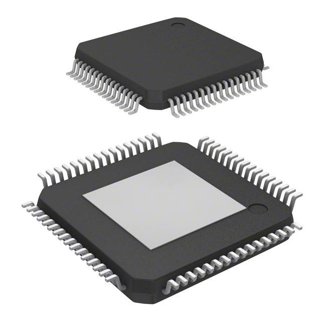
| 描述 | IC MCU 16BIT 64KB FLASH 100QFP |
| EEPROM容量 | - |
| 产品分类 | |
| I/O数 | 85 |
| 品牌 | Renesas Electronics America |
| 数据手册 | |
| 产品图片 |
|
| 产品型号 | M30622F8PFP#U5C |
| RAM容量 | 4K x 8 |
| rohs | 无铅 / 符合限制有害物质指令(RoHS)规范要求 |
| 产品系列 | M16C™ M16C/60/62P |
| 产品培训模块 | http://www.digikey.cn/PTM/IndividualPTM.page?site=cn&lang=zhs&ptm=15037 |
| 产品目录页面 | |
| 供应商器件封装 | 100-QFP(14x20) |
| 其它名称 | M30622F8PFPU5C |
| 包装 | 托盘 |
| 外设 | DMA,WDT |
| 封装/外壳 | 100-BQFP |
| 工作温度 | -20°C ~ 85°C |
| 振荡器类型 | 内部 |
| 数据转换器 | A/D 26x10b; D/A 2x8b |
| 标准包装 | 1 |
| 核心处理器 | M16C/60 |
| 核心尺寸 | 16-位 |
| 特色产品 | http://www.digikey.com/product-highlights/cn/zh/segger-microcontroller-systems-flasher-tools/3226 |
| 电压-电源(Vcc/Vdd) | 2.7 V ~ 5.5 V |
| 程序存储器类型 | 闪存 |
| 程序存储容量 | 64KB(64K x 8) |
| 连接性 | I²C, IEBus, UART/USART |
| 速度 | 24MHz |
| 配用 | /product-detail/zh/QSK-62P%20PLUS/867-1000-ND/2095293/product-detail/zh/R0K33062PS001BE/R0K33062PS001BE-ND/2002693 |


- 商务部:美国ITC正式对集成电路等产品启动337调查
- 曝三星4nm工艺存在良率问题 高通将骁龙8 Gen1或转产台积电
- 太阳诱电将投资9.5亿元在常州建新厂生产MLCC 预计2023年完工
- 英特尔发布欧洲新工厂建设计划 深化IDM 2.0 战略
- 台积电先进制程称霸业界 有大客户加持明年业绩稳了
- 达到5530亿美元!SIA预计今年全球半导体销售额将创下新高
- 英特尔拟将自动驾驶子公司Mobileye上市 估值或超500亿美元
- 三星加码芯片和SET,合并消费电子和移动部门,撤换高东真等 CEO
- 三星电子宣布重大人事变动 还合并消费电子和移动部门
- 海关总署:前11个月进口集成电路产品价值2.52万亿元 增长14.8%


PDF Datasheet 数据手册内容提取
To our customers, Old Company Name in Catalogs and Other Documents On April 1st, 2010, NEC Electronics Corporation merged with Renesas Technology Corporation, and Renesas Electronics Corporation took over all the business of both companies. Therefore, although the old company name remains in this document, it is a valid Renesas Electronics document. We appreciate your understanding. Renesas Electronics website: http://www.renesas.com April 1st, 2010 Renesas Electronics Corporation Issued by: Renesas Electronics Corporation (http://www.renesas.com) Send any inquiries to http://www.renesas.com/inquiry.
Notice 1. All information included in this document is current as of the date this document is issued. Such information, however, is subject to change without any prior notice. Before purchasing or using any Renesas Electronics products listed herein, please confirm the latest product information with a Renesas Electronics sales office. Also, please pay regular and careful attention to additional and different information to be disclosed by Renesas Electronics such as that disclosed through our website. 2. Renesas Electronics does not assume any liability for infringement of patents, copyrights, or other intellectual property rights of third parties by or arising from the use of Renesas Electronics products or technical information described in this document. No license, express, implied or otherwise, is granted hereby under any patents, copyrights or other intellectual property rights of Renesas Electronics or others. 3. You should not alter, modify, copy, or otherwise misappropriate any Renesas Electronics product, whether in whole or in part. 4. Descriptions of circuits, software and other related information in this document are provided only to illustrate the operation of semiconductor products and application examples. You are fully responsible for the incorporation of these circuits, software, and information in the design of your equipment. Renesas Electronics assumes no responsibility for any losses incurred by you or third parties arising from the use of these circuits, software, or information. 5. When exporting the products or technology described in this document, you should comply with the applicable export control laws and regulations and follow the procedures required by such laws and regulations. You should not use Renesas Electronics products or the technology described in this document for any purpose relating to military applications or use by the military, including but not limited to the development of weapons of mass destruction. Renesas Electronics products and technology may not be used for or incorporated into any products or systems whose manufacture, use, or sale is prohibited under any applicable domestic or foreign laws or regulations. 6. Renesas Electronics has used reasonable care in preparing the information included in this document, but Renesas Electronics does not warrant that such information is error free. Renesas Electronics assumes no liability whatsoever for any damages incurred by you resulting from errors in or omissions from the information included herein. 7. Renesas Electronics products are classified according to the following three quality grades: “Standard”, “High Quality”, and “Specific”. The recommended applications for each Renesas Electronics product depends on the product’s quality grade, as indicated below. You must check the quality grade of each Renesas Electronics product before using it in a particular application. You may not use any Renesas Electronics product for any application categorized as “Specific” without the prior written consent of Renesas Electronics. Further, you may not use any Renesas Electronics product for any application for which it is not intended without the prior written consent of Renesas Electronics. Renesas Electronics shall not be in any way liable for any damages or losses incurred by you or third parties arising from the use of any Renesas Electronics product for an application categorized as “Specific” or for which the product is not intended where you have failed to obtain the prior written consent of Renesas Electronics. The quality grade of each Renesas Electronics product is “Standard” unless otherwise expressly specified in a Renesas Electronics data sheets or data books, etc. “Standard”: Computers; office equipment; communications equipment; test and measurement equipment; audio and visual equipment; home electronic appliances; machine tools; personal electronic equipment; and industrial robots. “High Quality”: Transportation equipment (automobiles, trains, ships, etc.); traffic control systems; anti-disaster systems; anti- crime systems; safety equipment; and medical equipment not specifically designed for life support. “Specific”: Aircraft; aerospace equipment; submersible repeaters; nuclear reactor control systems; medical equipment or systems for life support (e.g. artificial life support devices or systems), surgical implantations, or healthcare intervention (e.g. excision, etc.), and any other applications or purposes that pose a direct threat to human life. 8. You should use the Renesas Electronics products described in this document within the range specified by Renesas Electronics, especially with respect to the maximum rating, operating supply voltage range, movement power voltage range, heat radiation characteristics, installation and other product characteristics. Renesas Electronics shall have no liability for malfunctions or damages arising out of the use of Renesas Electronics products beyond such specified ranges. 9. Although Renesas Electronics endeavors to improve the quality and reliability of its products, semiconductor products have specific characteristics such as the occurrence of failure at a certain rate and malfunctions under certain use conditions. Further, Renesas Electronics products are not subject to radiation resistance design. Please be sure to implement safety measures to guard them against the possibility of physical injury, and injury or damage caused by fire in the event of the failure of a Renesas Electronics product, such as safety design for hardware and software including but not limited to redundancy, fire control and malfunction prevention, appropriate treatment for aging degradation or any other appropriate measures. Because the evaluation of microcomputer software alone is very difficult, please evaluate the safety of the final products or system manufactured by you. 10. Please contact a Renesas Electronics sales office for details as to environmental matters such as the environmental compatibility of each Renesas Electronics product. Please use Renesas Electronics products in compliance with all applicable laws and regulations that regulate the inclusion or use of controlled substances, including without limitation, the EU RoHS Directive. Renesas Electronics assumes no liability for damages or losses occurring as a result of your noncompliance with applicable laws and regulations. 11. This document may not be reproduced or duplicated, in any form, in whole or in part, without prior written consent of Renesas Electronics. 12. Please contact a Renesas Electronics sales office if you have any questions regarding the information contained in this document or Renesas Electronics products, or if you have any other inquiries. (Note 1) “Renesas Electronics” as used in this document means Renesas Electronics Corporation and also includes its majority- owned subsidiaries. (Note 2) “Renesas Electronics product(s)” means any product developed or manufactured by or for Renesas Electronics.
M16C/62P Group (M16C/62P, M16C/62PT) REJ03B0001-0241 SINGLE-CHIP 16-BIT CMOS MICROCOMPUTER Rev.2.41 Jan 10, 2006 1. Overview The M16C/62P Group (M16C/62P, M16C/62PT) of single-chip microcomputers are built using the high performance silicon gate CMOS process using a M16C/60 Series CPU core and are packaged in a 80-pin, 100-pin and 128-pin plastic molded QFP. These single-chip microcomputers operate using sophisticated instructions featuring a high level of instruction efficiency. With 1M bytes of address space, they are capable of executing instructions at high speed. In addition, this microcomputer contains a multiplier and DMAC which combined with fast instruction processing capability, makes it suitable for control of various OA, communication, and industrial equipment which requires high- speed arithmetic/logic operations. 1.1 Applications Audio, cameras, television, home appliance, office/communications/portable/industrial equipment, automobile, etc. Specifications written in this manual are believed to be accurate, but are not guaranteed to be entirely free of error. Specifications in this manual may be changed for functional or performance improvements. Please make sure your manual is the latest edition. Rev.2.41 Jan 10, 2006 Page 1 of 96 REJ03B0001-0241
M16C/62P Group (M16C/62P, M16C/62PT) 1. Overview 1.2 Performance Outline Table 1.1 to 1.3 list Performance Outline of M16C/62P Group (M16C/62P, M16C/62PT)(128-pin version). Table 1.1 Performance Outline of M16C/62P Group (M16C/62P, M16C/62PT)(128-pin version) Item Performance M16C/62P CPU Number of Basic Instructions 91 instructions Minimum Instruction Execution 41.7ns(f(BCLK)=24MHz, VCC1=3.3 to 5.5V) Time 100ns(f(BCLK)=10MHz, VCC1=2.7 to 5.5V) Operating Mode Single-chip, memory expansion and microprocessor mode Address Space 1 Mbyte (Available to 4 Mbytes by memory space expansion function) Memory Capacity See Table 1.4 to 1.5 Product List Peripheral Port Input/Output : 113 pins, Input : 1 pin Function Multifunction Timer Timer A : 16 bits x 5 channels, Timer B : 16 bits x 6 channels, Three phase motor control circuit Serial Interface 3 channels Clock synchronous, UART, I2C bus(1), IEBus(2) 2 channels Clock synchronous A/D Converter 10-bit A/D converter: 1 circuit, 26 channels D/A Converter 8 bits x 2 channels DMAC 2 channels CRC Calculation Circuit CCITT-CRC Watchdog Timer 15 bits x 1 channel (with prescaler) Interrupt Internal: 29 sources, External: 8 sources, Software: 4 sources, Priority level: 7 levels Clock Generation Circuit 4 circuits Main clock generation circuit (*), Subclock generation circuit (*), On-chip oscillator, PLL synthesizer (*)Equipped with a built-in feedback resistor. Oscillation Stop Detection Stop detection of main clock oscillation, re-oscillation detection Function function Voltage Detection Circuit Available (option(4)) Electric Supply Voltage VCC1=3.0 to 5.5 V, VCC2=2.7V to VCC1 (f(BCLK=24MHz) Characteristics VCC1=2.7 to 5.5 V, VCC2=2.7V to VCC1 (f(BCLK=10MHz) Power Consumption 14 mA (VCC1=VCC2=5V, f(BCLK)=24MHz) 8 mA (VCC1=VCC2=3V, f(BCLK)=10MHz) 1.8µA (VCC1=VCC2=3V, f(XCIN)=32kHz, wait mode) 0.7µA (VCC1=VCC2=3V, stop mode) Flash memory Program/Erase Supply Voltage 3.3±0.3 V or 5.0±0.5 V version Program and Erase Endurance 100 times (all area) or 1,000 times (user ROM area without block A and block 1) / 10,000 times (block A, block 1) (3) Operating Ambient Temperature -20 to 85°C, -40 to 85°C (3) Package 128-pin plastic mold LQFP NOTES: 1. I2C bus is a registered trademark of Koninklijke Philips Electronics N. V. 2. IEBus is a registered trademark of NEC Electronics Corporation. 3. See Table 1.8 Product Code for the program and erase endurance, and operating ambient temperature. In addition 1,000 times/10,000 times are under development as of Jul., 2005. Please inquire about a release schedule. 4. All options are on request basis. Rev.2.41 Jan 10, 2006 Page 2 of 96 REJ03B0001-0241
M16C/62P Group (M16C/62P, M16C/62PT) 1. Overview Table 1.2 Performance Outline of M16C/62P Group (M16C/62P, M16C/62PT)(100-pin version) Item Performance M16C/62P M16C/62PT(4) CPU Number of Basic Instructions 91 instructions Minimum Instruction 41.7ns(f(BCLK)=24MHz, VCC1=3.3 to 5.5V) 41.7ns(f(BCLK)=24MHz, VCC1=4.0 to 5.5V) Execution Time 100ns(f(BCLK)=10MHz, VCC1=2.7 to 5.5V) Operating Mode Single-chip, memory expansion Single-chip and microprocessor mode Address Space 1 Mbyte (Available to 4 Mbytes by 1 Mbyte memory space expansion function) Memory Capacity See Table 1.4 to 1.7 Product List Peripheral Port Input/Output : 87 pins, Input : 1 pin Function Multifunction Timer Timer A : 16 bits x 5 channels, Timer B : 16 bits x 6 channels, Three phase motor control circuit Serial Interface 3 channels Clock synchronous, UART, I2C bus(1), IEBus(2) 2 channels Clock synchronous A/D Converter 10-bit A/D converter: 1 circuit, 26 channels D/A Converter 8 bits x 2 channels DMAC 2 channels CRC Calculation Circuit CCITT-CRC Watchdog Timer 15 bits x 1 channel (with prescaler) Interrupt Internal: 29 sources, External: 8 sources, Software: 4 sources, Priority level: 7 levels Clock Generation Circuit 4 circuits Main clock generation circuit (*), Subclock generation circuit (*), On-chip oscillator, PLL synthesizer (*)Equipped with a built-in feedback resistor. Oscillation Stop Stop detection of main clock oscillation, re-oscillation detection function Detection Function Voltage Detection Circuit Available (option (5)) Absent Electric Supply Voltage VCC1=3.0 to 5.5 V, VCC2=2.7V to VCC1=VCC2=4.0 to 5.5V Characteristics VCC1 (f(BCLK=24MHz) (f(BCLK=24MHz) VCC1=2.7 to 5.5 V, VCC2=2.7V to VCC1 (f(BCLK=10MHz) Power Consumption 14 mA (VCC1=VCC2=5V, f(BCLK)=24MHz) 14 mA (VCC1=VCC2=5V, f(BCLK)=24MHz) 8 mA (VCC1=VCC2=3V, f(BCLK)=10MHz) 2.0µA (VCC1=VCC2=5V, f(XCIN)=32kHz, 1.8µA (VCC1=VCC2=3V, f(XCIN)=32kHz, wait mode) wait mode) 0.8µA (VCC1=VCC2=5V, stop mode) 0.7µA (VCC1=VCC2=3V, stop mode) Flash memory Program/Erase Supply Voltage 3.3±0.3 V or 5.0±0.5 V 5.0±0.5 V version Program and Erase 100 times (all area) Endurance or 1,000 times (user ROM area without block A and block 1) / 10,000 times (block A, block 1) (3) Operating Ambient Temperature -20 to 85°C, T version : -40 to 85°C -40 to 85°C (3) V version : -40 to 125°C Package 100-pin plastic mold QFP, LQFP NOTES: 1. I2C bus is a registered trademark of Koninklijke Philips Electronics N. V. 2. IEBus is a registered trademark of NEC Electronics Corporation. 3. See Table 1.8 and 1.9 Product Code for the program and erase endurance, and operating ambient temperature. In addition 1,000 times/10,000 times are under development as of Jul., 2005. Please inquire about a release schedule. 4. Use the M16C/62PT on VCC1=VCC2 5. All options are on request basis. Rev.2.41 Jan 10, 2006 Page 3 of 96 REJ03B0001-0241
M16C/62P Group (M16C/62P, M16C/62PT) 1. Overview Table 1.3 Performance Outline of M16C/62P Group (M16C/62P, M16C/62PT)(80-pin version) Item Performance M16C/62P M16C/62PT(4) CPU Number of Basic Instructions 91 instructions Minimum Instruction 41.7ns(f(BCLK)=24MHz, VCC1=3.3 to 5.5V) 41.7ns(f(BCLK)=24MHz, VCC1=4.0 to 5.5V) Execution Time 100ns(f(BCLK)=10MHz, VCC1=2.7 to 5.5V) Operating Mode Single-chip mode Address Space 1 Mbyte Memory Capacity See Table 1.4 to 1.7 Product List Peripheral Port Input/Output : 70 pins, Input : 1 pin Function Multifunction Timer Timer A : 16 bits x 5 channels (Timer A1 and A2 are internal timer), Timer B : 16 bits x 6 channels (Timer B1 is internal timer) Serial Interface 2 channels Clock synchronous, UART, I2C bus(1), IEBus(2) 1 channel Clock synchronous, I2C bus(1), IEBus(2) 2 channels Clock synchronous (1 channel is only transmission) A/D Converter 10-bit A/D converter: 1 circuit, 26 channels D/A Converter 8 bits x 2 channels DMAC 2 channels CRC Calculation Circuit CCITT-CRC Watchdog Timer 15 bits x 1 channel (with prescaler) Interrupt Internal: 29 sources, External: 5 sources, Software: 4 sources, Priority level: 7 levels Clock Generation Circuit 4 circuits Main clock generation circuit (*), Subclock generation circuit (*), On-chip oscillator, PLL synthesizer (*)Equipped with a built-in feedback resistor. Oscillation Stop Stop detection of main clock oscillation, re-oscillation detection function Detection Function Voltage Detection Circuit Available (option (4)) Absent Electric Supply Voltage VCC1=3.0 to 5.5 V, (f(BCLK=24MHz) VCC1=4.0 to 5.5V, (f(BCLK=24MHz) Characteristics VCC1=2.7 to 5.5 V, (f(BCLK=10MHz) Power Consumption 14 mA (VCC1=5V, f(BCLK)=24MHz) 14 mA (VCC1=5V, f(BCLK)=24MHz) 8 mA (VCC1=3V, f(BCLK)=10MHz) 2.0µA (VCC1=5V, f(XCIN)=32kHz, 1.8µA (VCC1=3V, f(XCIN)=32kHz, wait mode) wait mode) 0.8µA (VCC1=5V, stop mode) 0.7µA (VCC1=3V, stop mode) Flash memory Program/Erase Supply Voltage 3.3 ± 0.3V or 5.0 ± 0.5V 5.0 ± 0.5V version Program and Erase 100 times (all area) Endurance or 1,000 times (user ROM area without block A and block 1) / 10,000 times (block A, block 1) (3) Operating Ambient Temperature -20 to 85°C, T version : -40 to 85°C -40 to 85°C (3) V version : -40 to 125°C Package 80-pin plastic mold QFP NOTES: 1. I2C bus is a registered trademark of Koninklijke Philips Electronics N. V. 2. IEBus is a registered trademark of NEC Electronics Corporation. 3. See Table 1.8 and 1.9 Product Code for the program and erase endurance, and operating ambient temperature. In addition 1,000 times/10,000 times are under development as of Jul., 2005. Please inquire about a release schedule. 4. All options are on request basis. Rev.2.41 Jan 10, 2006 Page 4 of 96 REJ03B0001-0241
M16C/62P Group (M16C/62P, M16C/62PT) 1. Overview 1.3 Block Diagram Figure 1.1 is a M16C/62P Group (M16C/62P, M16C/62PT) 128-pin and 100-pin version Block Diagram, Figure 1.2 is a M16C/62P Group (M16C/62P, M16C/62PT) 80-pin version Block Diagram. 8 8 8 8 8 8 8 Port P0 Port P1 Port P2 Port P3 Port P4 Port P5 Port P6 <VCC2 ports>(4) <VCC1 ports>(4) P o Internal peripheral functions rt P 8 A/D converter System clock 7 (10 bits X 8 channels generation circuit Timer (16-bit) Expandable up to 26 channels) P XIN-XOUT o OInuptpuut t( t(itmimeer rB A):) :6 5 clock syncUhAroRnTo uosr serial I/O PLL freXqCuIeNn-cXyC sOyUntThesizer rt P8 7 (8 bits X 3 channels) On-chip oscillator < Three-phase motor V control circuit CRC arithmetic circuit (CCITT ) Clock synchronous serial I/O CC Po (Polynomial : X16+X12+X5+1) (8 bits X 2 channels) 1 p rt P M16C/60 series16-bit CPU core Memory orts 8_5 > (4 Watchdog timer R0H R0L SB ROM (1) ) Po (15 bits) R1H R2R1L USP rt P 8 ISP 9 R3 RAM (2) DMAC INTB (2 channels) A0 PC P A1 o D/A converter FB FLG rt P (8 bits X 2 channels) Multiplier 1 8 0 <VCC1 ports>(4) <VCC2 ports>(4) Port P11 Port P14 Port P12 Port P13 (3) (3) (3) (3) 8 2 8 8 NOTES : 1. ROM size depends on microcomputer type. 2. RAM size depends on microcomputer type. 3. Ports P11 to P14 exist only in 128-pin version. 4. Use M16C/62PT on VCC1= VCC2. Figure 1.1 M16C/62P Group (M16C/62P, M16C/62PT) 128-pin and 100-pin version Block Diagram Rev.2.41 Jan 10, 2006 Page 5 of 96 REJ03B0001-0241
M16C/62P Group (M16C/62P, M16C/62PT) 1. Overview 8 8 8 4 8 8 Port P0 Port P2 Port P3 Port P4 Port P5 Port P6 (4) P o rt P 4 Internal peripheral functions A/D converter System clock 7 Timer (16-bit) (10 bits X 8 channels generation circuit Expandable up to 26 channels) XIN-XOUT P OInuptuptu (tt i(mtimere Br )A: )6: 5 UcloAcRkT s oynrchronous serial I/O(2 channels) PLL freXqCuIeNn-cXyC sOyUntThesizer ort P 7 UART (1 channel) On-chip oscillator 8 (3) Clock synchronous serial I/O P C(RPCo lyanriothmmiaelt i:c X c1i6rc+uXi1t 2(+CXC5I+T1T) ) (8 bits X 2 channels) (4) ort P 8 _ 5 Watchdog timer M16C/60 series16-bit CPU core Memory (15 bits) RR10HH RR10LL SB ROM (1) Po (2 DchManAnCels) RR23 UISSPP RAM (2) rt P9 7 INTB A0 D/A converter A1 PC P (8 bits X 2 channels) FB FLG o Multiplier rt P 1 8 0 NOTES : 1. ROM size depends on microcomputer type. 2. RAM size depends on microcomputer type. 3. To use a UART2, set the CRD bit in the U2C0 register to “1” (CTS/RTS function disabled). 4. There is no external connections for port P1, P4_4 to P4_7, P7_2 to P7_5 and P9_1 in 80-pin version. Set the direction bits in these ports to “1” (output mode), and set the output data to “0” (“L”) using the program. Figure 1.2 M16C/62P Group (M16C/62P, M16C/62PT) 80-pin version Block Diagram Rev.2.41 Jan 10, 2006 Page 6 of 96 REJ03B0001-0241
M16C/62P Group (M16C/62P, M16C/62PT) 1. Overview 1.4 Product List Table 1.4 to 1.7 list the product list, Figure 1.3 shows the Type No., Memory Size, and Package, Table 1.8 lists the Product Code of Flash Memory version and ROMless version for M16C/62P, and Table 1.9 lists the Product Code of Flash Memory version for M16C/62PT. Figure 1.4 shows the Marking Diagram of Flash Memory version and ROM-less version for M16C/62P (Top View), and Figure 1.5 shows the Marking Diagram of Flash Memory version for M16C/62PT (Top View) at the time of ROM order. Table 1.4 Product List (1) (M16C/62P) As of Dec. 2005 Type No. ROM Capacity RAM Capacity Package Type (1) Remarks M30622M6P-XXXFP 48 Kbytes 4 Kbytes PRQP0100JB-A Mask ROM version M30622M6P-XXXGP PLQP0100KB-A M30622M8P-XXXFP 64 Kbytes 4 Kbytes PRQP0100JB-A M30622M8P-XXXGP PLQP0100KB-A M30623M8P-XXXGP PRQP0080JA-A M30622MAP-XXXFP 96 Kbytes 5 Kbytes PRQP0100JB-A M30622MAP-XXXGP PLQP0100KB-A M30623MAP-XXXGP PRQP0080JA-A M30620MCP-XXXFP 128 Kbytes 10 Kbytes PRQP0100JB-A M30620MCP-XXXGP PLQP0100KB-A M30621MCP-XXXGP PRQP0080JA-A M30622MEP-XXXFP 192 Kbytes 12 Kbytes PRQP0100JB-A M30622MEP-XXXGP PLQP0100KB-A M30623MEP-XXXGP PLQP0128KB-A M30622MGP-XXXFP 256 Kbytes 12 Kbytes PRQP0100JB-A M30622MGP-XXXGP PLQP0100KB-A M30623MGP-XXXGP PLQP0128KB-A M30624MGP-XXXFP 20 Kbytes PRQP0100JB-A M30624MGP-XXXGP PLQP0100KB-A M30625MGP-XXXGP PLQP0128KB-A M30622MWP-XXXFP 320 Kbytes 16 Kbytes PRQP0100JB-A M30622MWP-XXXGP PLQP0100KB-A M30623MWP-XXXGP PLQP0128KB-A M30624MWP-XXXFP 24 Kbytes PRQP0100JB-A M30624MWP-XXXGP PLQP0100KB-A M30625MWP-XXXGP PLQP0128KB-A M30626MWP-XXXFP 31 Kbytes PRQP0100JB-A M30626MWP-XXXGP PLQP0100KB-A M30627MWP-XXXGP PLQP0128KB-A (D): Under development NOTES: 1. The old package type numbers of each package type are as follows. PLQP0128KB-A : 128P6Q-A, PRQP0100JB-A : 100P6S-A, PLQP0100KB-A : 100P6Q-A, PRQP0080JA-A : 80P6S-A Rev.2.41 Jan 10, 2006 Page 7 of 96 REJ03B0001-0241
M16C/62P Group (M16C/62P, M16C/62PT) 1. Overview Table 1.5 Product List (2) (M16C/62P) As of Dec. 2005 RAM Type No. ROM Capacity Package Type (1) Remarks Capacity M30622MHP-XXXFP 384 Kbytes 16 Kbytes PRQP0100JB-A Mask ROM version M30622MHP-XXXGP PLQP0100KB-A M30623MHP-XXXGP PLQP0128KB-A M30624MHP-XXXFP 24 Kbytes PRQP0100JB-A M30624MHP-XXXGP PLQP0100KB-A M30625MHP-XXXGP PLQP0128KB-A M30626MHP-XXXFP 31 Kbytes PRQP0100JB-A M30626MHP-XXXGP PLQP0100KB-A M30627MHP-XXXGP PLQP0128KB-A M30626MJP-XXXFP (D) 512 Kbytes 31 Kbytes PRQP0100JB-A M30626MJP-XXXGP (D) PLQP0100KB-A M30627MJP-XXXGP (D) PLQP0128KB-A M30622F8PFP 64K+4 Kbytes 4 Kbytes PRQP0100JB-A Flash memory M30622F8PGP PLQP0100KB-A version (2) M30623F8PGP PRQP0080JA-A M30620FCPFP 128K+4 Kbytes 10 Kbytes PRQP0100JB-A M30620FCPGP PLQP0100KB-A M30621FCPGP PRQP0080JA-A M3062LFGPFP(3) (D) 256K+4 Kbytes 20 Kbytes PRQP0100JB-A M3062LFGPGP(3) (D) PLQP0100KB-A M30625FGPGP PLQP0128KB-A M30626FHPFP 384K+4 Kbytes 31 Kbytes PRQP0100JB-A M30626FHPGP PLQP0100KB-A M30627FHPGP PLQP0128KB-A M30626FJPFP 512K+4 Kbytes 31 Kbytes PRQP0100JB-A M30626FJPGP PLQP0100KB-A M30627FJPGP PLQP0128KB-A M30622SPFP − 4 Kbytes PRQP0100JB-A ROM-less version M30622SPGP PLQP0100KB-A M30620SPFP 10 Kbytes PRQP0100JB-A M30620SPGP PLQP0100KB-A M30624SPFP (D) − 20 Kbytes PRQP0100JB-A M30624SPGP (D) PLQP0100KB-A M30626SPFP (D) 31 Kbytes PRQP0100JB-A M30626SPGP (D) PLQP0100KB-A (D): Under development NOTES: 1. The old package type numbers of each package type are as follows. PLQP0128KB-A : 128P6Q-A, PRQP0100JB-A : 100P6S-A, PLQP0100KB-A : 100P6Q-A, PRQP0080JA-A : 80P6S-A 2. In the flash memory version, there is 4K bytes area (block A). 3. Please use M3062LFGPFP and M3062LFGPGP for your new system instead of M30624FGPFP and M30624FGPGP. The M16C/62P Group (M16C/62P, M16C/62PT) hardware manual is still good for M30624FGPFP and M30624FGPGP. M30624FGPFP 256K+4 Kbytes 20 Kbytes PRQP0100JB-A Flash memory version M30624FGPGP PLQP0100KB-A Rev.2.41 Jan 10, 2006 Page 8 of 96 REJ03B0001-0241
M16C/62P Group (M16C/62P, M16C/62PT) 1. Overview Table 1.6 Product List (3) (T version (M16C/62PT)) As of Dec. 2005 RAM Type No. ROM Capacity Package Type (1) Remarks Capacity M3062CM6T-XXXFP (D) 48 Kbytes 4 Kbytes PRQP0100JB-A Mask ROM T Version M3062CM6T-XXXGP (D) PLQP0100KB-A version (High reliability 85°C version) M3062EM6T-XXXGP (P) PRQP0080JA-A M3062CM8T-XXXFP (D) 64 Kbytes 4 Kbytes PRQP0100JB-A M3062CM8T-XXXGP (D) PLQP0100KB-A M3062EM8T-XXXGP (P) PRQP0080JA-A M3062CMAT-XXXFP (D) 96 Kbytes 5 Kbytes PRQP0100JB-A M3062CMAT-XXXGP (D) PLQP0100KB-A M3062EMAT-XXXGP (P) PRQP0080JA-A M3062AMCT-XXXFP (D) 128 Kbytes 10 Kbytes PRQP0100JB-A M3062AMCT-XXXGP (D) PLQP0100KB-A M3062BMCT-XXXGP (P) PRQP0080JA-A M3062CF8TFP (D) 64 K+4 Kbytes 4 Kbytes PRQP0100JB-A Flash M3062CF8TGP PLQP0100KB-A memory version (2) M3062AFCTFP (D) 128K+4 Kbytes 10 Kbytes PRQP0100JB-A M3062AFCTGP (D) PLQP0100KB-A M3062BFCTGP (P) PRQP0080JA-A M3062JFHTFP (D) 384K+4 Kbytes 31 Kbytes PRQP0100JB-A M3062JFHTGP (D) PLQP0100KB-A (D): Under development (P): Under planning NOTES: 1. The old package type numbers of each package type are as follows. PRQP0100JB-A : 100P6S-A, PLQP0100KB-A : 100P6Q-A, PRQP0080JA-A : 80P6S-A 2. In the flash memory version, there is 4K bytes area (block A). Rev.2.41 Jan 10, 2006 Page 9 of 96 REJ03B0001-0241
M16C/62P Group (M16C/62P, M16C/62PT) 1. Overview Table 1.7 Product List (4) (V version (M16C/62PT)) As of Dec. 2005 RAM Type No. ROM Capacity Package Type(1) Remarks Capacity M3062CM6V-XXXFP (P) 48 Kbytes 4 Kbytes PRQP0100JB-A Mask ROM V Version M3062CM6V-XXXGP (P) PLQP0100KB-A version (High reliability 125°C version) M3062EM6V-XXXGP (P) PRQP0080JA-A M3062CM8V-XXXFP (P) 64 Kbytes 4 Kbytes PRQP0100JB-A M3062CM8V-XXXGP (P) PLQP0100KB-A M3062EM8V-XXXGP (P) PRQP0080JA-A M3062CMAV-XXXFP (P) 96 Kbytes 5 Kbytes PRQP0100JB-A M3062CMAV-XXXGP (P) PLQP0100KB-A M3062EMAV-XXXGP (P) PRQP0080JA-A M3062AMCV-XXXFP (D) 128 Kbytes 10 Kbytes PRQP0100JB-A M3062AMCV-XXXGP (D) PLQP0100KB-A M3062BMCV-XXXGP (P) PRQP0080JA-A M3062AFCVFP (D) 128K+4 Kbytes 10 Kbytes PRQP0100JB-A Flash M3062AFCVGP (D) PLQP0100KB-A memory version (2) M3062BFCVGP (P) PRQP0080JA-A M3062JFHVFP (P) 384K+4 Kbytes 31 Kbytes PRQP0100JB-A M3062JFHVGP (P) PLQP0100KB-A (D): Under development (P): Under planning NOTES: 1. The old package type numbers of each package type are as follows. PLQP0128KB-A : 128P6Q-A, PRQP0100JB-A : 100P6S-A, PLQP0100KB-A : 100P6Q-A, PRQP0080JA-A : 80P6S-A 2. In the flash memory version, there is 4K bytes area (block A). Rev.2.41 Jan 10, 2006 Page 10 of 96 REJ03B0001-0241
M16C/62P Group (M16C/62P, M16C/62PT) 1. Overview Type No. M 3 0 6 2 6 M H P - X X X F P Package type: FP : Package PRQP0100JB-A (100P6S-A) GP : Package PRQP0080JA-A (80P6S-A), PLQP0100KB-A (100P6Q-A), PLQP0128KB-A (128P6Q-A), ROM No. Omitted for flash memory version and ROMless version Classification P : M16C/62P T : T version (M16C/62PT) V : V version (M16C/62PT) ROM capacity: 6: 48 Kbytes G: 256 Kbytes 8: 64 Kbytes W:320 Kbytes A: 96 Kbytes H: 384 Kbytes C: 128 Kbytes J: 512 Kbytes E: 192 Kbytes Memory type: M: Mask ROM version F: Flash memory version S: ROM-less version Shows RAM capacity, pin count, etc Numeric, Alphabet (L) : M16C/62P Alphabet (L is excluded.) : M16C/62PT M16C/62(P) Group M16C Family Figure 1.3 Type No., Memory Size, and Package Rev.2.41 Jan 10, 2006 Page 11 of 96 REJ03B0001-0241
M16C/62P Group (M16C/62P, M16C/62PT) 1. Overview Table 1.8 Product Code of Flash Memory version and ROMless version for M16C/62P Internal ROM Internal ROM (User ROM Area Without Block A, Product Block 1) (Block A, Block 1) Operating Package Ambient Code Program Temperature Program Temperature Temperature and Erase and Erase Range Range Endurance Endurance Flash memory D3 Lead- 100 0°C to 60°C 100 0°C to 60°C -40°C to 85°C Version included D5 -20°C to 85°C D7 1,000 10,000 -40°C to 85°C -40°C to 85°C D9 -20°C to 85°C -20°C to 85°C U3 Lead-free 100 100 0°C to 60°C -40°C to 85°C U5 -20°C to 85°C U7 1,000 10,000 -40°C to 85°C -40°C to 85°C U9 -20°C to 85°C -20°C to 85°C ROM-less D3 Lead- − − − − -40°C to 85°C version included D5 -20°C to 85°C U3 Lead-free − − − − -40°C to 85°C U5 -20°C to 85°C M1 6 C M3 0 6 2 6 F HP F P Type No. (See Figure 1.3 Type No., Memory Size, and Package) B D 5 Chip version and product code X X X X X X X B : Shows chip version. Henceforth, whenever it changes a version, it continues with B, C, and D. D5 : Shows Product code. (See table 1.8 Product Code) Date code seven digits The product without marking of chip version of the flash memory version and the ROMless version corresponds to the chip version “A”. Figure 1.4 Marking Diagram of Flash Memory version and ROM-less version for M16C/62P (Top View) Rev.2.41 Jan 10, 2006 Page 12 of 96 REJ03B0001-0241
M16C/62P Group (M16C/62P, M16C/62PT) 1. Overview Table 1.9 Product Code of Flash Memory version for M16C/62PT Internal ROM Internal ROM (User ROM Area (Block A, Block 1) Operating Product Without Block A, Block 1) Package Ambient Code Program Program Temperature Temperature Temperature and Erase and Erase Range Range Endurance Endurance Flash T Version B Lead- 100 0°C to 60°C 100 0°C to 60°C -40°C to 85°C memory V Version included -40°C to 125°C Version T Version B7 1,000 10,000 -40°C to 85°C -40°C to 85°C V Version -40°C to 125°C -40°C to 125°C T Version U Lead-free 100 100 0°C to 60°C -40°C to 85°C V Version -40°C to 125°C T Version U7 1,000 10,000 -40°C to 85°C -40°C to 85°C V Version -40°C to 125°C -40°C to 125°C M1 6 C M3 0 6 2 J F HT F P Type No. (See Figure 1.3 Type No., Memory Size, and Package) Y YY X X X X X XX Date code seven digits Product code. (See table 1.9 Product Code) “ ” : Product code “B” “ P B F ” : Product code “U” “ B 7 ” : Product code “B” “ U 7 ” : Product code “U7” NOTES: 1. : Blank Figure 1.5 Marking Diagram of Flash Memory version for M16C/62PT (Top View) Rev.2.41 Jan 10, 2006 Page 13 of 96 REJ03B0001-0241
M16C/62P Group (M16C/62P, M16C/62PT) 1. Overview 1.5 Pin Configuration Figures 1.6 to 1.9 show the Pin Configuration (Top View). PIN CONFIGURATION (top view) 0)1)2)3)4)5)6) 0/-)1/D2/D3/D4/D5/D6/D7/D DDDDDDDD NT3NT4NT50/A0(/1/A1(/2/A2(/3/A3(/4/A4(/5/A5(/6/A6(/7/A7(/ D7) 1_/19D1_2/D10 1_3/D111_4/D121_5/D13/I1_6/D14/I1_7/D15/I2_0/AN2_2_1/AN2_2_2/AN2_2_3/AN2_2_4/AN2_2_5/AN2_2_6/AN2_2_7/AN2_SS3_0/A8(/-/CC212_012_112_212_312_43_1/A93_2/A103_3/A113_4/A123_5/A133_6/A143_7/A154_0/A164_1/A174_2/A184_3/A194_4/CS04_5/CS14_6/CS24_7/CS3 PP PPPPPPPPPPPPPVPVPPPPPPPPPPPPPPPPPPPP 1021011009998979695949392919089888786858483828180797877767574737271706968676665 P1_0/D8 103 64 P12_5 P0_7/AN0_7/D7 104 <VCC2> (2) 63 P12_6 P0_6/AN0_6/D6 105 62 P12_7 P0_5/AN0_5/D5 106 61 P5_0/WRL/WR P0_4/AN0_4/D4 107 60 P5_1/WRH/BHE P0_3/AN0_3/D3 108 59 P5_2/RD P0_2/AN0_2/D2 109 58 P5_3/BCLK P0_1/AN0_1/D1 110 57 P13_0 P0_0/AN0_0/D0 111 56 P13_1 P11_7 112 55 P13_2 P11_6 113 54 P13_3 P11_5 114 53 P5_4/HLDA P11_4 115 M16C/62P Group (M16C/62P) 52 P5_5/HOLD P11_3 116 51 P5_6/ALE P11_2 117 50 P5_7/RDY/CLKOUT P11_1 118 49 P13_4 P11_0 119 48 P13_5 P10_7/AN7/KI3 120 47 P13_6 P10_6/AN6/KI2 121 46 P13_7 P10_5/AN5/KI1 122 45 P6_0/CTS0/RTS0 P10_4/AN4/KI0 123 44 P6_1/CLK0 P10_3/AN3 124 43 P6_2/RXD0/SCL0 P10_2/AN2 125 42 P6_3/TXD0/SDA0 P10_1A/VASNS1 112267 <VCC1> (2) 4401 PP66__45//CCTLKS11/RTS1/CTS0/CLKS1 P10_0/AN0 128 39 VSS 1 2 3 4 5 6 7 8 91011121314151617181920212223242526272829303132333435363738 NOT12E.. SPU:7se_ 0th aen Md 1P67C_1/6 a2rPeVREFT N oAVCC nch P9_7/ADTRG/SIN4VaCnP9_6/ANEX1/SOUT4nCe1P9_5/ANEX0/CLK4l =oVpP9_4/DA1/TB4INCenCP9_3/DA0/TB3IN-2d.rP9_2/TB2IN/SOUT3ainP9_1/TB1IN/SIN3 ouP9_0/TB0IN/CLK3tpuP14_1t pP14_0insBYTE. CNVSSP8_7/XCINP8_6/XCOUTRESETXOUTVSSXINVCC1P8_5/NMIP8_4/INT2/ZPP8_3/INT1P8_2/INT0P8_1/TA4IN/UP8_0/TA4OUT/UP7_7/TA3INP7_6/TA3OUT P7_5/TA2IN/WP7_4/TA2OUT/WP7_3/CTS2/RTS2/TA1IN/VP7_2/CLK2/TA1OUT/V_1/RXD2/SCL2/TA0IN/TB5IN (1) P7_0/TXD2/SDA2/TA0OUT(1) P6_7/TXD1/SDA1VCC1P6_6/RXD1/SCL1 7 P Package : PLQP0128KB-A (128P6Q-A) Figure 1.6 Pin Configuration (Top View) Rev.2.41 Jan 10, 2006 Page 14 of 96 REJ03B0001-0241
M16C/62P Group (M16C/62P, M16C/62PT) 1. Overview Table 1.10 Pin Characteristics for 128-Pin Package (1) Pin No. Control Pin Port Interrupt Pin Timer Pin UART Pin Analog Pin Bus Control Pin 1 VREF 2 AVCC 3 P9_7 SIN4 ADTRG 4 P9_6 SOUT4 ANEX1 5 P9_5 CLK4 ANEX0 6 P9_4 TB4IN DA1 7 P9_3 TB3IN DA0 8 P9_2 TB2IN SOUT3 9 P9_1 TB1IN SIN3 10 P9_0 TB0IN CLK3 11 P14_1 12 P14_0 13 BYTE 14 CNVSS 15 XCIN P8_7 16 XCOUT P8_6 17 RESET 18 XOUT 19 VSS 20 XIN 21 VCC1 22 P8_5 NMI 23 P8_4 INT2 ZP 24 P8_3 INT1 25 P8_2 INT0 26 P8_1 TA4IN/U 27 P8_0 TA4OUT/U 28 P7_7 TA3IN 29 P7_6 TA3OUT 30 P7_5 TA2IN/W 31 P7_4 TA2OUT/W 32 P7_3 TA1IN/V CTS2/RTS2 33 P7_2 TA1OUT/V CLK2 34 P7_1 TA0IN/TB5IN RXD2/SCL2 35 P7_0 TA0OUT TXD2/SDA2 36 P6_7 TXD1/SDA1 37 VCC1 38 P6_6 RXD1/SCL1 39 VSS 40 P6_5 CLK1 41 P6_4 CTS1/RTS1/CTS0/CLKS1 42 P6_3 TXD0/SDA0 43 P6_2 RXD0/SCL0 44 P6_1 CLK0 45 P6_0 CTS0/RTS0 46 P13_7 47 P13_6 48 P13_5 49 P13_4 50 P5_7 RDY/CLKOUT Rev.2.41 Jan 10, 2006 Page 15 of 96 REJ03B0001-0241
M16C/62P Group (M16C/62P, M16C/62PT) 1. Overview Table 1.11 Pin Characteristics for 128-Pin Package (2) Pin No. Control Pin Port Interrupt Pin Timer Pin UART Pin Analog Pin Bus Control Pin 51 P5_6 ALE 52 P5_5 HOLD 53 P5_4 HLDA 54 P13_3 55 P13_2 56 P13_1 57 P13_0 58 P5_3 BCLK 59 P5_2 RD 60 P5_1 WRH/BHE 61 P5_0 WRL/WR 62 P12_7 63 P12_6 64 P12_5 65 P4_7 CS3 66 P4_6 CS2 67 P4_5 CS1 68 P4_4 CS0 69 P4_3 A19 70 P4_2 A18 71 P4_1 A17 72 P4_0 A16 73 P3_7 A15 74 P3_6 A14 75 P3_5 A13 76 P3_4 A12 77 P3_3 A11 78 P3_2 A10 79 P3_1 A9 80 P12_4 81 P12_3 82 P12_2 83 P12_1 84 P12_0 85 VCC2 86 P3_0 A8(/-/D7) 87 VSS 88 P2_7 AN2_7 A7(/D7/D6) 89 P2_6 AN2_6 A6(/D6/D5) 90 P2_5 AN2_5 A5(/D5/D4) 91 P2_4 AN2_4 A4(/D4/D3) 92 P2_3 AN2_3 A3(/D3/D2) 93 P2_2 AN2_2 A2(/D2/D1) 94 P2_1 AN2_1 A1(/D1/D0) 95 P2_0 AN2_0 A0(/D0/-) 96 P1_7 INT5 D15 97 P1_6 INT4 D14 98 P1_5 INT3 D13 99 P1_4 D12 100 P1_3 D11 Rev.2.41 Jan 10, 2006 Page 16 of 96 REJ03B0001-0241
M16C/62P Group (M16C/62P, M16C/62PT) 1. Overview Table 1.12 Pin Characteristics for 128-Pin Package (3) Pin No. Control Pin Port Interrupt Pin Timer Pin UART Pin Analog Pin Bus Control Pin 101 P1_2 D10 102 P1_1 D9 103 P1_0 D8 104 P0_7 AN0_7 D7 105 P0_6 AN0_6 D6 106 P0_5 AN0_5 D5 107 P0_4 AN0_4 D4 108 P0_3 AN0_3 D3 109 P0_2 AN0_2 D2 110 P0_1 AN0_1 D1 111 P0_0 AN0_0 D0 112 P11_7 113 P11_6 114 P11_5 115 P11_4 116 P11_3 117 P11_2 118 P11_1 119 P11_0 120 P10_7 KI3 AN7 121 P10_6 KI2 AN6 122 P10_5 KI1 AN5 123 P10_4 KI0 AN4 124 P10_3 AN3 125 P10_2 AN2 126 P10_1 AN1 127 AVSS 128 P10_0 AN0 Rev.2.41 Jan 10, 2006 Page 17 of 96 REJ03B0001-0241
M16C/62P Group (M16C/62P, M16C/62PT) 1. Overview PIN CONFIGURATION (top view) 0)1)2)3)4)5)6) 0/-)1/D2/D3/D4/D5/D6/D7/D DDDDDDDD NT3NT4NT50/A0(/1/A1(/2/A2(/3/A3(/4/A4(/5/A5(/6/A6(/7/A7(/ D7) 8910111213/I14/I15/IN2_N2_N2_N2_N2_N2_N2_N2_ 8(/-/ 910111213141516171819 DDDDDDDDAAAAAAAA A AAAAAAAAAAA 1_0/1_1/1_2/1_3/1_4/1_5/1_6/1_7/2_0/2_1/2_2/2_3/2_4/2_5/2_6/2_7/SS3_0/CC23_1/3_2/3_3/3_4/3_5/3_6/3_7/4_0/4_1/4_2/4_3/ PPPPPPPPPPPPPPPPVPVPPPPPPPPPPP 807978777675747372717069686766656463626160595857565554535251 P0_7/AN0_7/D7 81 50 P4_4/CS0 P0_6/AN0_6/D6 82 <VCC2> (2) 49 P4_5/CS1 P0_5/AN0_5/D5 83 48 P4_6/CS2 P0_4/AN0_4/D4 84 47 P4_7/CS3 P0_3/AN0_3/D3 85 46 P5_0/WRL/WR P0_2/AN0_2/D2 86 45 P5_1/WRH/BHE P0_1/AN0_1/D1 87 44 P5_2/RD P0_0/AN0_0/D0 88 43 P5_3/BCLK P10_7/AN7/KI3 89 M16C/62P Group 42 P5_4/HLDA P10_6/AN6/KI2 90 41 P5_5/HOLD P10_5/AN5/KI1 91 (M16C/62P, M16C/62PT) 40 P5_6/ALE P10_4/AN4/KI0 92 39 P5_7/RDY/CLKOUT P10_3/AN3 93 38 P6_0/CTS0/RTS0 P10_2/AN2 94 37 P6_1/CLK0 P10_1/AN1 95 36 P6_2/RXD0/SCL0 AVSS 96 35 P6_3/TXD0/SDA0 P10_0/AN0 97 34 P6_4/CTS1/RTS1/CTS0/CLKS1 VREF 98 <VCC1> (2) 33 P6_5/CLK1 AVCC 99 32 P6_6/RXD1/SCL1 P9_7/ADTRG/SIN4 100 31 P6_7/TXD1/SDA1 1 2 3 4 5 6 7 8 9 101112131415161718192021222324252627282930 P9_6/ANEX1/SOUT4P9_5/ANEX0/CLK4P9_4/DA1/TB4INP9_3/DA0/TB3INP9_2/TB2IN/SOUT3P9_1/TB1IN/SIN3P9_0/TB0IN/CLK3BYTECNVSSP8_7/XCINP8_6/XCOUTRESETXOUTVSSXINVCC1P8_5/NMIP8_4/INT2/ZPP8_3/INT1P8_2/INT0P8_1/TA4IN/UP8_0/TA4OUT/UP7_7/TA3INP7_6/TA3OUTP7_5/TA2IN/WP7_4/TA2OUT/W3/CTS2/RTS2/TA1IN/VP7_2/CLK2/TA1OUT/V2/SCL2/TA0IN/TB5IN(1) TXD2/SDA2/TA0OUT(1) P7_ RXD7_0/ NOTES: 1/P 1. P7_0 and P7_1 are N channel open-drain output pins. 7_ 2. Use the M16C/62PT on VCC1=VCC2. P Package : PRQP0100JB-A (100P6S-A) Figure 1.7 Pin Configuration (Top View) Rev.2.41 Jan 10, 2006 Page 18 of 96 REJ03B0001-0241
M16C/62P Group (M16C/62P, M16C/62PT) 1. Overview PIN CONFIGURATION (top view) 0)1)2)3)4)5)6) 0/-)1/D2/D3/D4/D5/D6/D7/D DDDDDDDD NT3NT4NT50/A0(/1/A1(/2/A2(/3/A3(/4/A4(/5/A5(/6/A6(/7/A7(/ D7) 111213/I14/I15/IN2_N2_N2_N2_N2_N2_N2_N2_ 8(/-/ 91011121314151617 DDDDDAAAAAAAA A AAAAAAAAA 1_3/1_4/1_5/1_6/1_7/2_0/2_1/2_2/2_3/2_4/2_5/2_6/2_7/SS3_0/CC23_1/3_2/3_3/3_4/3_5/3_6/3_7/4_0/4_1/ PPPPPPPPPPPPPVPVPPPPPPPPP 75747372717069686766656463626160595857565554535251 P1_2/D10 76 50 P4_2/A18 P1_1/D9 77 <VCC2> (2) 49 P4_3/A19 P1_0/D8 78 48 P4_4/CS0 P0_7/AN0_7/D7 79 47 P4_5/CS1 P0_6/AN0_6/D6 80 46 P4_6/CS2 P0_5/AN0_5/D5 81 45 P4_7/CS3 P0_4/AN0_4/D4 82 44 P5_0/WRL/WR P0_3/AN0_3/D3 83 43 P5_1/WRH/BHE P0_2/AN0_2/D2 84 42 P5_2/RD P0_1/AN0_1/D1 85 41 P5_3/BCLK P0_0/AN0_0/D0 86 40 P5_4/HLDA P10_7/AN7/KI3 87 M16C/62P Group 39 P5_5/HOLD P10_6/AN6/KI2 88 38 P5_6/ALE (M16C/62P, M16C/62PT) P10_5/AN5/KI1 89 37 P5_7/RDY/CLKOUT P10_4/AN4/KI0 90 36 P6_0/CTS0/RTS0 P10_3/AN3 91 35 P6_1/CLK0 P10_2/AN2 92 34 P6_2/RXD0/SCL0 P10_1/AN1 93 33 P6_3/TXD0/SDA0 AVSS 94 32 P6_4/CTS1/RTS1/CTS0/CLKS1 P10_0/AN0 95 31 P6_5/CLK1 VREF 96 30 P6_6/RXD1/SCL1 AVCC 97 29 P6_7/TXD1/SDA1 P9_7/ADTRG/SIN4 98 <VCC1> (2) 28 P7_0/TXD2/SDA2/TA0OUT (1) P9_6/ANEX1/SOUT4 99 27 P7_1/RXD2/SCL2/TA0IN/TB5IN (1) P9_5/ANEX0/CLK4 100 26 P7_2/CLK2/TA1OUT/V 1 2 3 4 5 6 7 8 9 10111213141516171819202122232425 P9_4/DA1/TB4INP9_3/DA0/TB3INP9_2/TB2IN/SOUT3P9_1/TB1IN/SIN3P9_0/TB0IN/CLK3BYTECNVSSP8_7/XCINP8_6/XCOUTRESETXOUTVSSXINVCC1 P8_5/NMIP8_4/INT2/ZPP8_3/INT1P8_2/INT0P8_1/TA4IN/UP8_0/TA4OUT/UP7_7/TA3INP7_6/TA3OUTP7_5/TA2IN/WP7_4/TA2OUT/W CTS2/RTS2/TA1IN/V 3/ NOTES: 7_ 1. P7_0 and P7_1 are N channel open-drain output pins. P 2. Use the M16C/62PT on VCC1=VCC2. Package : PLQP0100KB-A (100P6Q-A) Figure 1.8 Pin Configuration (Top View) Rev.2.41 Jan 10, 2006 Page 19 of 96 REJ03B0001-0241
M16C/62P Group (M16C/62P, M16C/62PT) 1. Overview Table 1.13 Pin Characteristics for 100-Pin Package (1) Pin No. Control Pin Port Interrupt Pin Timer Pin UART Pin Analog Pin Bus Control Pin FP GP 1 99 P9_6 SOUT4 ANEX1 2 100 P9_5 CLK4 ANEX0 3 1 P9_4 TB4IN DA1 4 2 P9_3 TB3IN DA0 5 3 P9_2 TB2IN SOUT3 6 4 P9_1 TB1IN SIN3 7 5 P9_0 TB0IN CLK3 8 6 BYTE 9 7 CNVSS 10 8 XCIN P8_7 11 9 XCOUT P8_6 12 10 RESET 13 11 XOUT 14 12 VSS 15 13 XIN 16 14 VCC1 17 15 P8_5 NMI 18 16 P8_4 INT2 ZP 19 17 P8_3 INT1 20 18 P8_2 INT0 21 19 P8_1 TA4IN/U 22 20 P8_0 TA4OUT/U 23 21 P7_7 TA3IN 24 22 P7_6 TA3OUT 25 23 P7_5 TA2IN/W 26 24 P7_4 TA2OUT/W 27 25 P7_3 TA1IN/V CTS2/RTS2 28 26 P7_2 TA1OUT/V CLK2 29 27 P7_1 TA0IN/TB5IN RXD2/SCL2 30 28 P7_0 TA0OUT TXD2/SDA2 31 29 P6_7 TXD1/SDA1 32 30 P6_6 RXD1/SCL1 33 31 P6_5 CLK1 34 32 P6_4 CTS1/RTS1/CTS0/CLKS1 35 33 P6_3 TXD0/SDA0 36 34 P6_2 RXD0/SCL0 37 35 P6_1 CLK0 38 36 P6_0 CTS0/RTS0 39 37 P5_7 RDY/CLKOUT 40 38 P5_6 ALE 41 39 P5_5 HOLD 42 40 P5_4 HLAD 43 41 P5_3 BCLK 44 42 P5_2 RD 45 43 P5_1 WRH/BHE 46 44 P5_0 WRL/WR 47 45 P4_7 CS3 48 46 P4_6 CS2 49 47 P4_5 CS1 50 48 P4_4 CS0 Rev.2.41 Jan 10, 2006 Page 20 of 96 REJ03B0001-0241
M16C/62P Group (M16C/62P, M16C/62PT) 1. Overview Table 1.14 Pin Characteristics for 100-Pin Package (2) Pin No. Control Pin Port Interrupt Pin Timer Pin UART Pin Analog Pin Bus Control Pin FP GP 51 49 P4_3 A19 52 50 P4_2 A18 53 51 P4_1 A17 54 52 P4_0 A16 55 53 P3_7 A15 56 54 P3_6 A14 57 55 P3_5 A13 58 56 P3_4 A12 59 57 P3_3 A11 60 58 P3_2 A10 61 59 P3_1 A9 62 60 VCC2 63 61 P3_0 A8(/-/D7) 64 62 VSS 65 63 P2_7 AN2_7 A7(/D7/D6) 66 64 P2_6 AN2_6 A6(/D6/D5) 67 65 P2_5 AN2_5 A5(/D5/D4) 68 66 P2_4 AN2_4 A4(/D4/D3) 69 67 P2_3 AN2_3 A3(/D3/D2) 70 68 P2_2 AN2_2 A2(/D2/D1) 71 69 P2_1 AN2_1 A1(/D1/D0) 72 70 P2_0 AN2_0 A0(/D0/-) 73 71 P1_7 INT5 D15 74 72 P1_6 INT4 D14 75 73 P1_5 INT3 D13 76 74 P1_4 D12 77 75 P1_3 D11 78 76 P1_2 D10 79 77 P1_1 D9 80 78 P1_0 D8 81 79 P0_7 AN0_7 D7 82 80 P0_6 AN0_6 D6 83 81 P0_5 AN0_5 D5 84 82 P0_4 AN0_4 D4 85 83 P0_3 AN0_3 D3 86 84 P0_2 AN0_2 D2 87 85 P0_1 AN0_1 D1 88 86 P0_0 AN0_0 D0 89 87 P10_7 KI3 AN7 90 88 P10_6 KI2 AN6 91 89 P10_5 KI1 AN5 92 90 P10_4 KI0 AN4 93 91 P10_3 AN3 94 92 P10_2 AN2 95 93 P10_1 AN1 96 94 AVSS 97 95 P10_0 AN0 98 96 VREF 99 97 AVCC 100 98 P9_7 SIN4 ADTRG Rev.2.41 Jan 10, 2006 Page 21 of 96 REJ03B0001-0241
M16C/62P Group (M16C/62P, M16C/62PT) 1. Overview PIN CONFIGURATION (top view) 7 0 1 2 3 4 5 6 7 _ _ _ _ _ _ _ _ _ 0 2 2 2 2 2 2 2 2 N N N N N N N N N A A A A A A A A A 7/ 0/ 1/ 2/ 3/ 4/ 5/ 6/ 7/ 0 1 2 3 4 5 6 7 0 1 2 _ _ _ _ _ _ _ _ _ _ _ _ _ _ _ _ _ _ _ _ 0 2 2 2 2 2 2 2 2 3 3 3 3 3 3 3 3 4 4 4 P P P P P P P P P P P P P P P P P P P P 60 59 58 57 56 55 54 53 52 51 50 49 48 47 46 45 44 43 42 41 P0_6/AN0_6 61 40 P4_3 P0_5/AN0_5 62 39 P5_0 P0_4/AN0_4 63 38 P5_1 P0_3/AN0_3 64 37 P5_2 P0_2/AN0_2 65 36 P5_3 P0_1/AN0_1 66 35 P5_4 P0_0/AN0_0 67 34 P5_5 P10_7/AN7/KI3 68 33 P5_6 P10_6/AN6/KI2 69 M16C/62P Group 32 P5_7/CLKOUT P10_5/AN5/KI1 70 31 P6_0/CTS0/RTS0 P10_4/AN4/KI0 71 (M16C/62P, M16C/62PT) 30 P6_1/CLK0 P10_3/AN3 72 29 P6_2/RXD0/SCL0 P10_2/AN2 73 28 P6_3/TXD0/SDA0 P10_1/AN1 74 27 P6_4/CTS1/RTS1/CTS0/CLKS1 AVSS 75 26 P6_5/CLK1 P10_0/AN0 76 25 P6_6/RXD1/SCL1 VREF 77 24 P6_7/TXD1/SDA1 AVCC 78 23 P7_0/TXD2/SDA2/TA0OUT (1) P9_7/ADTRG/SIN4 79 22 P7_1/RXD2/SCL2/TA0IN/TB5IN (1) P9_6/ANEX1/SOUT4 80 21 P7_6/TA3OUT 1 2 3 4 5 6 7 8 9 10 11 12 13 14 15 16 17 18 19 20 P9_5/ANEX0/CLK4 P9_4/DA1/TB4IN P9_3/DA0/TB3IN P9_2/TB2IN/SOUT3 P9_0/TB0IN/CLK3CNVSS(BYTE) P8_7/XCIN P8_6/XCOUT RESET XOUT VSS XIN VCC1 P8_5/NMI P8_4/INT2/ZP P8_3/INT1 P8_2/INT0 P8_1/TA4IN P8_0/TA4OUT P7_7/TA3IN NOTES: 1. P7_0 and P7_1 are N channel open-drain output pins. Package : PRQP0080JA-A (80P6S-A) Figure 1.9 Pin Configuration (Top View) Rev.2.41 Jan 10, 2006 Page 22 of 96 REJ03B0001-0241
M16C/62P Group (M16C/62P, M16C/62PT) 1. Overview Table 1.15 Pin Characteristics for 80-Pin Package (1) Pin No. Control Pin Port Interrupt Pin Timer Pin UART Pin Analog Pin Bus Control Pin 1 P9_5 CLK4 ANEX0 2 P9_4 TB4IN DA1 3 P9_3 TB3IN DA0 4 P9_2 TB2IN SOUT3 5 P9_0 TB0IN CLK3 CNVSS 6 (BYTE) 7 XCIN P8_7 8 XCOUT P8_6 9 RESET 10 XOUT 11 VSS 12 XIN 13 VCC1 14 P8_5 NMI 15 P8_4 INT2 ZP 16 P8_3 INT1 17 P8_2 INT0 18 P8_1 TA4IN 19 P8_0 TA4OUT 20 P7_7 TA3IN 21 P7_6 TA3OUT 22 P7_1 TA0IN/TB5IN RXD2/SCL2 23 P7_0 TA0OUT TXD2/SDA2 24 P6_7 TXD1/SDA1 25 P6_6 RXD1/SCL1 26 P6_5 CLK1 27 P6_4 CTS1/RTS1/CTS0/CLKS1 28 P6_3 TXD0/SDA0 29 P6_2 RXD0/SCL0 30 P6_1 CLK0 31 P6_0 CTS0/RTS0 32 P5_7 CLKOUT 33 P5_6 34 P5_5 35 P5_4 36 P5_3 37 P5_2 38 P5_1 39 P5_0 40 P4_3 41 P4_2 42 P4_1 43 P4_0 44 P3_7 45 P3_6 46 P3_5 47 P3_4 48 P3_3 49 P3_2 50 P3_1 Rev.2.41 Jan 10, 2006 Page 23 of 96 REJ03B0001-0241
M16C/62P Group (M16C/62P, M16C/62PT) 1. Overview Table 1.16 Pin Characteristics for 80-Pin Package (2) Pin No. Control Pin Port Interrupt Pin Timer Pin UART Pin Analog Pin Bus Control Pin 51 P3_0 52 P2_7 AN2_7 53 P2_6 AN2_6 54 P2_5 AN2_5 55 P2_4 AN2_4 56 P2_3 AN2_3 57 P2_2 AN2_2 58 P2_1 AN2_1 59 P2_0 AN2_0 60 P0_7 AN0_7 61 P0_6 AN0_6 62 P0_5 AN0_5 63 P0_4 AN0_4 64 P0_3 AN0_3 65 P0_2 AN0_2 66 P0_1 AN0_1 67 P0_0 AN0_0 68 P10_7 KI3 AN7 69 P10_6 KI2 AN6 70 P10_5 KI1 AN5 71 P10_4 KI0 AN4 72 P10_3 AN3 73 P10_2 AN2 74 P10_1 AN1 75 AVSS 76 P10_0 AN0 77 VREF 78 AVCC 79 P9_7 SIN4 ADTRG 80 P9_6 SOUT4 ANEX1 Rev.2.41 Jan 10, 2006 Page 24 of 96 REJ03B0001-0241
M16C/62P Group (M16C/62P, M16C/62PT) 1. Overview 1.6 Pin Description Table 1.17 Pin Description (100-pin and 128-pin Version) (1) Signal Name Pin Name I/O Power Description Type Supply(3) Power supply VCC1,VCC2 I − Apply 2.7 to 5.5 V to the VCC1 and VCC2 pins and 0 V to the VSS input VSS pin. The VCC apply condition is that VCC1 ≥ VCC2. (1, 2) Analog power AVCC I VCC1 Applies the power supply for the A/D converter. Connect the AVCC supply input AVSS pin to VCC1. Connect the AVSS pin to VSS. Reset input RESET I VCC1 The microcomputer is in a reset state when applying “L” to the this pin. CNVSS CNVSS I VCC1 Switches processor mode. Connect this pin to VSS to when after a reset to start up in single-chip mode. Connect this pin to VCC1 to start up in microprocessor mode. External data BYTE I VCC1 Switches the data bus in external memory space. The data bus is bus width 16 bits long when the this pin is held "L" and 8 bits long when the select input this pin is held "H". Set it to either one. Connect this pin to VSS when an single-chip mode. Bus control D0 to D7 I/O VCC2 Inputs and outputs data (D0 to D7) when these pins are set as the pins (4) separate bus. D8 to D15 I/O VCC2 Inputs and outputs data (D8 to D15) when external 16-bit data bus is set as the separate bus. A0 to A19 O VCC2 Output address bits (A0 to A19). A0/D0 to I/O VCC2 Input and output data (D0 to D7) and output address bits (A0 to A7) by A7/D7 timesharing when external 8-bit data bus are set as the multiplexed bus. A1/D0 to I/O VCC2 Input and output data (D0 to D7) and output address bits (A1 to A8) A8/D7 by timesharing when external 16-bit data bus are set as the multiplexed bus. CS0 to CS3 O VCC2 Output CS0 to CS3 signals. CS0 to CS3 are chip-select signals to specify an external space. WRL/WR O VCC2 Output WRL, WRH, (WR, BHE), RD signals. WRL and WRH or WRH/BHE BHE and WR can be switched by program. RD • WRL, WRH and RD are selected The WRL signal becomes "L" by writing data to an even address in an external memory space. The WRH signal becomes "L" by writing data to an odd address in an external memory space. The RD pin signal becomes "L" by reading data in an external memory space. • WR, BHE and RD are selected The WR signal becomes "L" by writing data in an external memory space. The RD signal becomes "L" by reading data in an external memory space. The BHE signal becomes "L" by accessing an odd address. Select WR, BHE and RD for an external 8-bit data bus. ALE O VCC2 ALE is a signal to latch the address. HOLD I VCC2 While the HOLD pin is held "L", the microcomputer is placed in a hold state. HLDA O VCC2 In a hold state, HLDA outputs a "L" signal. RDY I VCC2 While applying a "L" signal to the RDY pin, the microcomputer is placed in a wait state. I : Input O : Output I/O : Input and output Power Supply : Power supplies which relate to the external bus pins are separated as VCC2, thus they can be interfaced using the different voltage as VCC1. NOTES: 1. In this manual, hereafter, VCC refers to VCC1 unless otherwise noted. 2. In M16C/62PT, apply 4.0 to 5.5 V to the VCC1 and VCC2 pins. Also the apply condition is that VCC1 = VCC2. 3. When use VCC1 > VCC2, contacts due to some points or restrictions to be checked. 4. Bus control pins in M16C/62PT cannot be used. Rev.2.41 Jan 10, 2006 Page 25 of 96 REJ03B0001-0241
M16C/62P Group (M16C/62P, M16C/62PT) 1. Overview Table 1.18 Pin Description (100-pin and 128-pin Version) (2) Signal Name Pin Name I/O Power Description Type Supply(1) Main clock XIN I VCC1 I/O pins for the main clock generation circuit. Connect a ceramic input resonator or crystal oscillator between XIN and XOUT (3). To use Main clock XOUT O VCC1 the external clock, input the clock from XIN and leave XOUT open. output Sub clock input XCIN I VCC1 I/O pins for a sub clock oscillation circuit. Connect a crystal Sub clock XCOUT O VCC1 oscillator between XCIN and XCOUT (3). To use the external clock, output input the clock from XCIN and leave XCOUT open. BCLK output (2) BCLK O VCC2 Outputs the BCLK signal. Clock output CLKOUT O VCC2 The clock of the same cycle as fC, f8, or f32 is outputted. INT interrupt INT0 to INT2 I VCC1 Input pins for the INT interrupt. input NT3 to INT5 I VCC2 NMI interrupt NMI I VCC1 Input pin for the NMI interrupt. Pin states can be read by the P8_5 input bit in the P8 register. Key input KI0 to KI3 I VCC1 Input pins for the key input interrupt. interrupt input Timer A TA0OUT to I/O VCC1 These are timer A0 to timer A4 I/O pins. (however, output of TA4OUT TA0OUT for the N-channel open drain output.) TA0IN to I VCC1 These are timer A0 to timer A4 input pins. TA4IN ZP I VCC1 Input pin for the Z-phase. Timer B TB0IN to I VCC1 These are timer B0 to timer B5 input pins. TB5IN Three-phase U, U, V, V, O VCC1 These are Three-phase motor control output pins. motor control W, W output Serial interface CTS0 to I VCC1 These are send control input pins. CTS2 RTS0 to O VCC1 These are receive control output pins. RTS2 CLK0 to I/O VCC1 These are transfer clock I/O pins. CLK4 RXD0 to I VCC1 These are serial data input pins. RXD2 SIN3, SIN4 I VCC1 These are serial data input pins. TXD0 to O VCC1 These are serial data output pins. (however, output of TXD2 for the TXD2 N-channel open drain output.) SOUT3, O VCC1 These are serial data output pins. SOUT4 CLKS1 O VCC1 This is output pin for transfer clock output from multiple pins function. I2C mode SDA0 to I/O VCC1 These are serial data I/O pins. (however, output of SDA2 for the N- SDA2 channel open drain output.) SCL0 to I/O VCC1 These are transfer clock I/O pins. (however, output of SCL2 for the SCL2 N-channel open drain output.) I : Input O : Output I/O : Input and output NOTES: 1. When use VCC1 > VCC2, contacts due to some points or restrictions to be checked. 2. This pin function in M16C/62PT cannot be used. 3. Ask the oscillator maker the oscillation characteristic. Rev.2.41 Jan 10, 2006 Page 26 of 96 REJ03B0001-0241
M16C/62P Group (M16C/62P, M16C/62PT) 1. Overview Table 1.19 Pin Description (100-pin and 128-pin Version) (3) Signal Name Pin Name I/O Power Description Type Supply(1) Reference VREF I VCC1 Applies the reference voltage for the A/D converter and D/A voltage input converter. A/D converter AN0 to AN7, I VCC1 Analog input pins for the A/D converter. AN0_0 to AN0_7, AN2_0 to AN2_7 ADTRG I VCC1 This is an A/D trigger input pin. ANEX0 I/O VCC1 This is the extended analog input pin for the A/D converter, and is the output in external op-amp connection mode. ANEX1 I VCC1 This is the extended analog input pin for the A/D converter. D/A converter DA0, DA1 O VCC1 This is the output pin for the D/A converter. I/O port P0_0 to P0_7, I/O VCC2 8-bit I/O ports in CMOS, having a direction register to select an P1_0 to P1_7, input or output. P2_0 to P2_7, Each pin is set as an input port or output port. An input port can P3_0 to P3_7, be set for a pull-up or for no pull-up in 4-bit unit by program. P4_0 to P4_7, P5_0 to P5_7, P12_0 to P12_7 (2), P13_0 to P13_7 (2) P6_0 to P6_7, I/O VCC1 8-bit I/O ports having equivalent functions to P0. P7_0 to P7_7, (however, output of P7_0 and P7_1 for the N-channel open drain P9_0 to P9_7, output.) P10_0 to P10_7, P11_0 to P11_7 (2) P8_0 to P8_4, I/O VCC1 I/O ports having equivalent functions to P0. P8_6, P8_7, P14_0, P14_1(2) Input port P8_5 I VCC1 Input pin for the NMI interrupt. Pin states can be read by the P8_5 bit in the P8 register. I : Input O : Output I/O : Input and output NOTES: 1. When use VCC1 > VCC2, contacts due to some points or restrictions to be checked. 2. Ports P11 to P14 in M16C/62P (100-pin version) and M16C/62PT (100-pin version) cannot be used. Rev.2.41 Jan 10, 2006 Page 27 of 96 REJ03B0001-0241
M16C/62P Group (M16C/62P, M16C/62PT) 1. Overview Table 1.20 Pin Description (80-pin Version) (1) (1) Signal Name Pin Name I/O Power Description Type Supply Power supply VCC1, VSS I − Apply 2.7 to 5.5 V to the VCC1 pin and 0 V to the VSS pin. (1, 2) input Analog power AVCC I VCC1 Applies the power supply for the A/D converter. Connect the supply input AVSS AVCC pin to VCC1. Connect the AVSS pin to VSS. Reset input RESET I VCC1 The microcomputer is in a reset state when applying “L” to the this pin. CNVSS CNVSS I VCC1 Switches processor mode. Connect this pin to VSS to when after a (BYTE) reset to start up in single-chip mode. Connect this pin to VCC1 to start up in microprocessor mode. As for the BYTE pin of the 80-pin versions, pull-up processing is performed within the microcomputer. Main clock XIN I VCC1 I/O pins for the main clock generation circuit. Connect a ceramic input resonator or crystal oscillator between XIN and XOUT (3). To use Main clock XOUT O VCC1 the external clock, input the clock from XIN and leave XOUT output open. Sub clock input XCIN I VCC1 I/O pins for a sub clock oscillation circuit. Connect a crystal Sub clock XCOUT O VCC1 oscillator between XCIN and XCOUT (3). To use the external output clock, input the clock from XCIN and leave XCOUT open. Clock output CLKOUT O VCC2 The clock of the same cycle as fC, f8, or f32 is outputted. INT interrupt INT0 to INT2 I VCC1 Input pins for the INT interrupt. input NMI interrupt NMI I VCC1 Input pin for the NMI interrupt. input Key input KI0 to KI3 I VCC1 Input pins for the key input interrupt. interrupt input Timer A TA0OUT, I/O VCC1 These are Timer A0,Timer A3 and Timer A4 I/O pins. (however, TA3OUT, output of TA0OUT for the N-channel open drain output.) TA4OUT TA0IN, TA3IN, I VCC1 These are Timer A0, Timer A3 and Timer A4 input pins. TA4IN ZP I VCC1 Input pin for the Z-phase. Timer B TB0IN, TB2IN I VCC1 These are Timer B0, Timer B2 to Timer B5 input pins. to TB5IN Serial interface CTS0 to CTS1 I VCC1 These are send control input pins. RTS0 to RTS1 O VCC1 These are receive control output pins. CLK0, CLK1, I/O VCC1 These are transfer clock I/O pins. CLK3, CLK4 RXD0 to RXD2 I VCC1 These are serial data input pins. SIN4 I VCC1 This is serial data input pin. TXD0 to TXD2 O VCC1 These are serial data output pins. (however, output of TXD2 for the N-channel open drain output.) SOUT3, O VCC1 These are serial data output pins. SOUT4 CLKS1 O VCC1 This is output pin for transfer clock output from multiple pins function. I2C mode SDA0 to SDA2 I/O VCC1 These are serial data I/O pins. (however, output of SDA2 for the N-channel open drain output.) SCL0 to SCL2 I/O VCC1 These are transfer clock I/O pins. (however, output of SCL2 for the N-channel open drain output.) I : Input O : Output I/O : Input and output NOTES: 1. In this manual, hereafter, VCC refers to VCC1 unless otherwise noted. 2. In M16C/62PT, apply 4.0 to 5.5 V to the VCC1 pin. 3. Ask the oscillator maker the oscillation characteristic. Rev.2.41 Jan 10, 2006 Page 28 of 96 REJ03B0001-0241
M16C/62P Group (M16C/62P, M16C/62PT) 1. Overview Table 1.21 Pin Description (80-pin Version) (2) Signal Name Pin Name I/O Power Description Type Supply(1) Reference VREF I VCC1 Applies the reference voltage for the A/D converter and D/A voltage input converter. A/D converter AN0 to AN7, I VCC1 Analog input pins for the A/D converter. AN0_0 to AN0_7, AN2_0 to AN2_7 ADTRG I VCC1 This is an A/D trigger input pin. ANEX0 I/O VCC1 This is the extended analog input pin for the A/D converter, and is the output in external op-amp connection mode. ANEX1 I VCC1 This is the extended analog input pin for the A/D converter. D/A converter DA0, DA1 O VCC1 This is the output pin for the D/A converter. I/O port (1) P0_0 to P0_7, I/O VCC1 8-bit I/O ports in CMOS, having a direction register to select an P2_0 to P2_7, input or output. P3_0 to P3_7, Each pin is set as an input port or output port. An input port can P5_0 to P5_7, be set for a pull-up or for no pull-up in 4-bit unit by program. P6_0 to P6_7, P10_0 to P10_7 P8_0 to P8_4, I/O VCC1 I/O ports having equivalent functions to P0. P8_6, P8_7, P9_0, P9_2 to P9_7 P4_0 to P4_3, I/O VCC1 I/O ports having equivalent functions to P0. P7_0, P7_1, (however, output of P7_0 and P7_1 for the N-channel open drain P7_6, P7_7 output.) Input port P8_5 I VCC1 Input pin for the NMI interrupt. Pin states can be read by the P8_5 bit in the P8 register. I : Input O : Output I/O : Input and output NOTES: 1. There is no external connections for port P1, P4_4 to P4_7, P7_2 to P7_5 and P9_1 in 80-pin version. Set the direction bits in these ports to “1” (output mode), and set the output data to “0” (“L”) using the program. Rev.2.41 Jan 10, 2006 Page 29 of 96 REJ03B0001-0241
M16C/62P Group (M16C/62P, M16C/62PT) 2. Central Processing Unit (CPU) 2. Central Processing Unit (CPU) Figure 2.1 shows the CPU registers. The CPU has 13 registers. Of these, R0, R1, R2, R3, A0, A1 and FB comprise a register bank. There are two register banks. b31 b15 b8b7 b0 R2 R0H R0L R3 R1H R1L Data Registers (1) R2 R3 A0 Address Registers (1) A1 FB Frame Base Registers (1) b19 b15 b0 INTBH INTBL Interrupt Table Register b19 b0 PC Program Counter b15 b0 USP User Stack Pointer ISP Interrupt Stack Pointer SB Static Base Register b15 b0 FLG Flag Register b15 b8 b7 b0 IPL U I O B S Z D C Carry Flag Debug Flag Zero Flag Sign Flag Register Bank Select Flag Overflow Flag Interrupt Enable Flag Stack Pointer Select Flag Reserved Area Processor Interrupt Priority Level Reserved Area NOTES: 1. These registers comprise a register bank. There are two register banks. Figure 2.1 Central Processing Unit Register 2.1 Data Registers (R0, R1, R2 and R3) The R0 register consists of 16 bits, and is used mainly for transfers and arithmetic/logic operations. R1 to R3 are the same as R0. The R0 register can be separated between high (R0H) and low (R0L) for use as two 8-bit data registers. R1H and R1L are the same as R0H and R0L. Conversely, R2 and R0 can be combined for use as a 32-bit data register (R2R0). R3R1 is the same as R2R0. Rev.2.41 Jan 10, 2006 Page 30 of 96 REJ03B0001-0241
M16C/62P Group (M16C/62P, M16C/62PT) 2. Central Processing Unit (CPU) 2.2 Address Registers (A0 and A1) The register A0 consists of 16 bits, and is used for address register indirect addressing and address register relative addressing. They also are used for transfers and logic/logic operations. A1 is the same as A0. In some instructions, registers A1 and A0 can be combined for use as a 32-bit address register (A1A0). 2.3 Frame Base Register (FB) FB is configured with 16 bits, and is used for FB relative addressing. 2.4 Interrupt Table Register (INTB) INTB is configured with 20 bits, indicating the start address of an interrupt vector table. 2.5 Program Counter (PC) PC is configured with 20 bits, indicating the address of an instruction to be executed. 2.6 User Stack Pointer (USP) and Interrupt Stack Pointer (ISP) Stack pointer (SP) comes in two types: USP and ISP, each configured with 16 bits. Your desired type of stack pointer (USP or ISP) can be selected by the U flag of FLG. 2.7 Static Base Register (SB) SB is configured with 16 bits, and is used for SB relative addressing. 2.8 Flag Register (FLG) FLG consists of 11 bits, indicating the CPU status. 2.8.1 Carry Flag (C Flag) This flag retains a carry, borrow, or shift-out bit that has occurred in the arithmetic/logic unit. 2.8.2 Debug Flag (D Flag) The D flag is used exclusively for debugging purpose. During normal use, it must be set to “0”. 2.8.3 Zero Flag (Z Flag) This flag is set to “1” when an arithmetic operation resulted in 0; otherwise, it is “0”. 2.8.4 Sign Flag (S Flag) This flag is set to “1” when an arithmetic operation resulted in a negative value; otherwise, it is “0”. 2.8.5 Register Bank Select Flag (B Flag) Register bank 0 is selected when this flag is “0” ; register bank 1 is selected when this flag is “1”. 2.8.6 Overflow Flag (O Flag) This flag is set to “1” when the operation resulted in an overflow; otherwise, it is “0”. 2.8.7 Interrupt Enable Flag (I Flag) This flag enables a maskable interrupt. Maskable interrupts are disabled when the I flag is “0”, and are enabled when the I flag is “1”. The I flag is cleared to “0” when the interrupt request is accepted. Rev.2.41 Jan 10, 2006 Page 31 of 96 REJ03B0001-0241
M16C/62P Group (M16C/62P, M16C/62PT) 2. Central Processing Unit (CPU) 2.8.8 Stack Pointer Select Flag (U Flag) ISP is selected when the U flag is “0”; USP is selected when the U flag is “1”. The U flag is cleared to “0” when a hardware interrupt request is accepted or an INT instruction for software interrupt Nos. 0 to 31 is executed. 2.8.9 Processor Interrupt Priority Level (IPL) IPL is configured with three bits, for specification of up to eight processor interrupt priority levels from level 0 to level 7. If a requested interrupt has priority greater than IPL, the interrupt is enabled. 2.8.10 Reserved Area When write to this bit, write “0”. When read, its content is indeterminate. Rev.2.41 Jan 10, 2006 Page 32 of 96 REJ03B0001-0241
M16C/62P Group (M16C/62P, M16C/62PT) 3. Memory 3. Memory Figure 3.1 is a Memory Map of the M16C/62P group. The address space extends the 1M bytes from address 00000h to FFFFFh. The internal ROM is allocated in a lower address direction beginning with address FFFFFh. For example, a 64-Kbyte internal ROM is allocated to the addresses from F0000h to FFFFFh. As for the flash memory version, 4-Kbyte space (block A) exists in 0F000h to 0FFFFh. 4-Kbyte space is mainly for storing data. In addition to storing data, 4-Kbyte space also can store programs. The fixed interrupt vector table is allocated to the addresses from FFFDCh to FFFFFh. Therefore, store the start address of each interrupt routine here. The internal RAM is allocated in an upper address direction beginning with address 00400h. For example, a 10-Kbyte internal RAM is allocated to the addresses from 00400h to 02BFFh. In addition to storing data, the internal RAM also stores the stack used when calling subroutines and when interrupts are generated. The SRF is allocated to the addresses from 00000h to 003FFh. Peripheral function control registers are located here. Of the SFR, any area which has no functions allocated is reserved for future use and cannot be used by users. The special page vector table is allocated to the addresses from FFE00h to FFFDBh. This vector is used by the JMPS or JSRS instruction. For details, refer to the M16C/60 and M16C/20 Series Software Manual. In memory expansion and microprocessor modes, some areas are reserved for future use and cannot be used by users. Use M16C/62P (80-pin version) and M16C/62PT in single-chip mode. The memory expansion and microprocessor modes cannot be used . 00000h SFR 00400h Internal RAM XXXXXh Reserved area (1) FFE00h 0F000h Internal ROM (data area) (3) 0FFFFh Special page 10000h vector table Internal RAM Internal ROM (3) External area Size Address XXXXXh Size Address YYYYYh 27000h 45 KKbbyytteess 001173FFFFhh 4684 KKbbyytteess FF04000000hh Reserved area FFFDCh Undefined instruction 28000h Overflow 10 Kbytes 02BFFh 96 Kbytes E8000h External area BRK instruction 12 Kbytes 033FFh 128 Kbytes E0000h 80000h Address match 16 Kbytes 043FFh 192 Kbytes D0000h Reserved area (2) Single step 20 Kbytes 053FFh 256 Kbytes C0000h YYYYYh Watchdog timer 24 Kbytes 063FFh 320 Kbytes B0000h Internal ROM DBC 31 Kbytes 07FFFh 384 Kbytes A0000h (program area) (5) NMI 512 Kbytes 80000h FFFFFh FFFFFh Reset NOTES: 1. During memory expansion and microprocessor modes, can be used. 2. In memory expansion mode, can be used. 3. As for the flash memory version, 4-Kbyte space (block A) exists. 4. Shown here is a memory map for the case where the PM10 bit in the PM1 register is “1” and the PM13 bit in the PM1 register is “1”. 5. When using the masked ROM version, write nothing to internal ROM area. Figure 3.1 Memory Map Rev.2.41 Jan 10, 2006 Page 33 of 96 REJ03B0001-0241
M16C/62P Group (M16C/62P, M16C/62PT) 4. Special Function Register (SFR) 4. Special Function Register (SFR) SFR(Special Function Register) is the control register of peripheral functions. Tables 4.1 to 4.6 list the SFR information. Table 4.1 SFR Information (1) (1) Address Register Symbol After Reset 0000h 0001h 0002h 0003h 0004h Processor Mode Register 0 (2) PM0 00000000b(CNVSS pin is “L”) 00000011b(CNVSS pin is “H”) 0005h Processor Mode Register 1 PM1 00001000b 0006h System Clock Control Register 0 CM0 01001000b 0007h System Clock Control Register 1 CM1 00100000b 0008h Chip Select Control Register (6) CSR 00000001b 0009h Address Match Interrupt Enable Register AIER XXXXXX00b 000Ah Protect Register PRCR XX000000b 000Bh Data Bank Register (6) DBR 00h 000Ch Oscillation Stop Detection Register (3) CM2 0X000000b 000Dh 000Eh Watchdog Timer Start Register WDTS XXh 000Fh Watchdog Timer Control Register WDC 00XXXXXXb (4) 0010h Address Match Interrupt Register 0 RMAD0 00h 0011h 00h 0012h X0h 0013h 0014h Address Match Interrupt Register 1 RMAD1 00h 0015h 00h 0016h X0h 0017h 0018h 0019h Voltage Detection Register 1 (5, 6) VCR1 00001000b 001Ah Voltage Detection Register 2 (5, 6) VCR2 00h 001Bh Chip Select Expansion Control Register (6) CSE 00h 001Ch PLL Control Register 0 PLC0 0001X010b 001Dh 001Eh Processor Mode Register 2 PM2 XXX00000b 001Fh Low Voltage Detection Interrupt Register (6) D4INT 00h 0020h DMA0 Source Pointer SAR0 XXh 0021h XXh 0022h XXh 0023h 0024h DMA0 Destination Pointer DAR0 XXh 0025h XXh 0026h XXh 0027h 0028h DMA0 Transfer Counter TCR0 XXh 0029h XXh 002Ah 002Bh 002Ch DMA0 Control Register DM0CON 00000X00b 002Dh 002Eh 002Fh 0030h DMA1 Source Pointer SAR1 XXh 0031h XXh 0032h XXh 0033h 0034h DMA1 Destination Pointer DAR1 XXh 0035h XXh 0036h XXh 0037h 0038h DMA1 Transfer Counter TCR1 XXh 0039h XXh 003Ah 003Bh 003Ch DMA1 Control Register DM1CON 00000X00b 003Dh 003Eh 003Fh NOTES: 1. The blank areas are reserved and cannot be accessed by users. 2. The PM00 and PM01 bits do not change at software reset, watchdog timer reset and oscillation stop detection reset. 3. The CM20, CM21, and CM27 bits do not change at oscillation stop detection reset. 4. The WDC5 bit is “0” (cold start) immediately after power-on. I t can only be set to “1” in a program. 5. This register does not change at software reset, watchdog timer reset and oscillation stop detection reset. 6. This register in M16C/62PT cannot be used. X : Nothing is mapped to this bit Rev.2.41 Jan 10, 2006 Page 34 of 96 REJ03B0001-0241
M16C/62P Group (M16C/62P, M16C/62PT) 4. Special Function Register (SFR) Table 4.2 SFR Information (2) (1) Address Register Symbol After Reset 0040h 0041h 0042h 0043h 0044h INT3 Interrupt Control Register INT3IC XX00X000b 0045h Timer B5 Interrupt Control Register TB5IC XXXXX000b 0046h Timer B4 Interrupt Control Register, UART1 BUS Collision Detection Interrupt Control Register TB4IC, U1BCNIC XXXXX000b 0047h Timer B3 Interrupt Control Register, UART0 BUS Collision Detection Interrupt Control Register TB3IC, U0BCNIC XXXXX000b 0048h SI/O4 Interrupt Control Register, INT5 Interrupt Control Register S4IC, INT5IC XX00X000b 0049h SI/O3 Interrupt Control Register, INT4 Interrupt Control Register S3IC, INT4IC XX00X000b 004Ah UART2 Bus Collision Detection Interrupt Control Register BCNIC XXXXX000b 004Bh DMA0 Interrupt Control Register DM0IC XXXXX000b 004Ch DMA1 Interrupt Control Register DM1IC XXXXX000b 004Dh Key Input Interrupt Control Register KUPIC XXXXX000b 004Eh A/D Conversion Interrupt Control Register ADIC XXXXX000b 004Fh UART2 Transmit Interrupt Control Register S2TIC XXXXX000b 0050h UART2 Receive Interrupt Control Register S2RIC XXXXX000b 0051h UART0 Transmit Interrupt Control Register S0TIC XXXXX000b 0052h UART0 Receive Interrupt Control Register S0RIC XXXXX000b 0053h UART1 Transmit Interrupt Control Register S1TIC XXXXX000b 0054h UART1 Receive Interrupt Control Register S1RIC XXXXX000b 0055h Timer A0 Interrupt Control Register TA0IC XXXXX000b 0056h Timer A1 Interrupt Control Register TA1IC XXXXX000b 0057h Timer A2 Interrupt Control Register TA2IC XXXXX000b 0058h Timer A3 Interrupt Control Register TA3IC XXXXX000b 0059h Timer A4 Interrupt Control Register TA4IC XXXXX000b 005Ah Timer B0 Interrupt Control Register TB0IC XXXXX000b 005Bh Timer B1 Interrupt Control Register TB1IC XXXXX000b 005Ch Timer B2 Interrupt Control Register TB2IC XXXXX000b 005Dh INT0 Interrupt Control Register INT0IC XX00X000b 005Eh INT1 Interrupt Control Register INT1IC XX00X000b 005Fh INT2 Interrupt Control Register INT2IC XX00X000b 0060h 0061h 0062h 0063h 0064h 0065h 0066h 0067h 0068h 0069h 006Ah 006Bh 006Ch 006Dh 006Eh 006Fh 0070h 0071h 0072h 0073h 0074h 0075h 0076h 0077h 0078h 0079h 007Ah 007Bh 007Ch 007Dh 007Eh 007Fh NOTES: 1. The blank areas are reserved and cannot be accessed by users. X : Nothing is mapped to this bit Rev.2.41 Jan 10, 2006 Page 35 of 96 REJ03B0001-0241
M16C/62P Group (M16C/62P, M16C/62PT) 4. Special Function Register (SFR) Table 4.3 SFR Information (3) (1) Address Register Symbol After Reset 0080h 0081h 0082h 0083h 0084h 0085h 0086h 0087h to 01AFh 01B0h 01B1h 01B2h 01B3h 01B4h Flash Identification Register (2) FIDR XXXXXX00b 01B5h Flash Memory Control Register 1 (2) FMR1 0X00XX0Xb 01B6h 01B7h Flash Memory Control Register 0 (2) FMR0 00000001b 01B8h Address Match Interrupt Register 2 RMAD2 00h 01B9h 00h 01BAh XXh 01BBh Address Match Interrupt Enable Register 2 AIER2 XXXXXX00b 01BCh Address Match Interrupt Register 3 RMAD3 00h 01BDh 00h 01BEh XXh 01C0h to 024Fh 0250h 0251h 0252h 0253h 0254h 0255h 0256h 0257h 0258h 0259h 025Ah 025Bh 025Ch 025Dh 025Eh Peripheral Clock Select Register PCLKR 00000011b 025Fh 0260h to 032Fh 0330h 0331h 0332h 0333h 0334h 0335h 0336h 0337h 0338h 0339h 033Ah 033Bh 033Ch 033Dh 033Eh 033Fh NOTES: 1. The blank areas are reserved and cannot be accessed by users. 2. This register is included in the flash memory version. X : Nothing is mapped to this bit Rev.2.41 Jan 10, 2006 Page 36 of 96 REJ03B0001-0241
M16C/62P Group (M16C/62P, M16C/62PT) 4. Special Function Register (SFR) Table 4.4 SFR Information (4) (1) Address Register Symbol After Reset 0340h Timer B3, 4, 5 Count Start Flag TBSR 000XXXXXb 0341h 0342h Timer A1-1 Register TA11 XXh 0343h XXh 0344h Timer A2-1 Register TA21 XXh 0345h XXh 0346h Timer A4-1 Register TA41 XXh 0347h XXh 0348h Three-Phase PWM Control Register 0 INVC0 00h 0349h Three-Phase PWM Control Register 1 INVC1 00h 034Ah Three-Phase Output Buffer Register 0 IDB0 00h 034Bh Three-Phase Output Buffer Register 1 IDB1 00h 034Ch Dead Time Timer DTT XXh 034Dh Timer B2 Interrupt Occurrence Frequency Set Counter ICTB2 XXh 034Eh 034Fh 0350h Timer B3 Register TB3 XXh 0351h XXh 0352h Timer B4 Register TB4 XXh 0353h XXh 0354h Timer B5 Register TB5 XXh 0355h XXh 0356h 0357h 0358h 0359h 035Ah 035Bh Timer B3 Mode Register TB3MR 00XX0000b 035Ch Timer B4 Mode Register TB4MR 00XX0000b 035Dh Timer B5 Mode Register TB5MR 00XX0000b 035Eh Interrupt Factor Select Register 2 IFSR2A 00XXXXXXb 035Fh Interrupt Factor Select Register IFSR 00h 0360h SI/O3 Transmit/Receive Register S3TRR XXh 0361h 0362h SI/O3 Control Register S3C 01000000b 0363h SI/O3 Bit Rate Generator S3BRG XXh 0364h SI/O4 Transmit/Receive Register S4TRR XXh 0365h 0366h SI/O4 Control Register S4C 01000000b 0367h SI/O4 Bit Rate Generator S4BRG XXh 0368h 0369h 036Ah 036Bh 036Ch UART0 Special Mode Register 4 U0SMR4 00h 036Dh UART0 Special Mode Register 3 U0SMR3 000X0X0Xb 036Eh UART0 Special Mode Register 2 U0SMR2 X0000000b 036Fh UART0 Special Mode Register U0SMR X0000000b 0370h UART1 Special Mode Register 4 U1SMR4 00h 0371h UART1 Special Mode Register 3 U1SMR3 000X0X0Xb 0372h UART1 Special Mode Register 2 U1SMR2 X0000000b 0373h UART1 Special Mode Register U1SMR X0000000b 0374h UART2 Special Mode Register 4 U2SMR4 00h 0375h UART2 Special Mode Register 3 U2SMR3 000X0X0Xb 0376h UART2 Special Mode Register 2 U2SMR2 X0000000b 0377h UART2 Special Mode Register U2SMR X0000000b 0378h UART2 Transmit/Receive Mode Register U2MR 00h 0379h UART2 Bit Rate Generator U2BRG XXh 037Ah UART2 Transmit Buffer Register U2TB XXh 037Bh XXh 037Ch UART2 Transmit/Receive Control Register 0 U2C0 00001000b 037Dh UART2 Transmit/Receive Control Register 1 U2C1 00000010b 037Eh UART2 Receive Buffer Register U2RB XXh 037Fh XXh NOTES: 1. The blank areas are reserved and cannot be accessed by users. X : Nothing is mapped to this bit Rev.2.41 Jan 10, 2006 Page 37 of 96 REJ03B0001-0241
M16C/62P Group (M16C/62P, M16C/62PT) 4. Special Function Register (SFR) Table 4.5 SFR Information (5) (1) Address Register Symbol After Reset 0380h Count Start Flag TABSR 00h 0381h Clock Prescaler Reset Fag CPSRF 0XXXXXXXb 0382h One-Shot Start Flag ONSF 00h 0383h Trigger Select Register TRGSR 00h 0384h Up-Down Flag UDF 00h (2) 0385h 0386h Timer A0 Register TA0 XXh 0387h XXh 0388h Timer A1 Register TA1 XXh 0389h XXh 038Ah Timer A2 Register TA2 XXh 038Bh XXh 038Ch Timer A3 Register TA3 XXh 038Dh XXh 038Eh Timer A4 Register TA4 XXh 038Fh XXh 0390h Timer B0 Register TB0 XXh 0391h XXh 0392h Timer B1 Register TB1 XXh 0393h XXh 0394h Timer B2 Register TB2 XXh 0395h XXh 0396h Timer A0 Mode Register TA0MR 00h 0397h Timer A1 Mode Register TA1MR 00h 0398h Timer A2 Mode Register TA2MR 00h 0399h Timer A3 Mode Register TA3MR 00h 039Ah Timer A4 Mode Register TA4MR 00h 039Bh Timer B0 Mode Register TB0MR 00XX0000b 039Ch Timer B1 Mode Register TB1MR 00XX0000b 039Dh Timer B2 Mode Register TB2MR 00XX0000b 039Eh Timer B2 Special Mode Register TB2SC XXXXXX00b 039Fh 03A0h UART0 Transmit/Receive Mode Register U0MR 00h 03A1h UART0 Bit Rate Generator U0BRG XXh 03A2h UART0 Transmit Buffer Register U0TB XXh 03A3h XXh 03A4h UART0 Transmit/Receive Control Register 0 U0C0 00001000b 03A5h UART0 Transmit/Receive Control Register 1 U0C1 00XX0010b 03A6h UART0 Receive Buffer Register U0RB XXh 03A7h XXh 03A8h UART1 Transmit/Receive Mode Register U1MR 00h 03A9h UART1 Bit Rate Generator U1BRG XXh 03AAh UART1 Transmit Buffer Register U1TB XXh 03ABh XXh 03ACh UART1 Transmit/Receive Control Register 0 U1C0 00001000b 03ADh UART1 Transmit/Receive Control Register 1 U1C1 00XX0010b 03AEh UART1 Receive Buffer Register U1RB XXh 03AFh XXh 03B0h UART Transmit/Receive Control Register 2 UCON X0000000b 03B1h 03B2h 03B3h 03B4h 03B5h 03B6h 03B7h 03B8h DMA0 Request Factor Select Register DM0SL 00h 03B9h 03BAh DMA1 Request Factor Select Register DM1SL 00h 03BBh 03BCh CRC Data Register CRCD XXh 03BDh XXh 03BEh CRC Input Register CRCIN XXh 03BFh NOTES: 1. The blank areas are reserved and cannot be accessed by users. 2. Bit 5 in the Up-down flag is “0” by reset. However, The values in these bits when read are indeterminate. X : Nothing is mapped to this bit Rev.2.41 Jan 10, 2006 Page 38 of 96 REJ03B0001-0241
M16C/62P Group (M16C/62P, M16C/62PT) 4. Special Function Register (SFR) Table 4.6 SFR Information (6) (1) Address Register Symbol After Reset 03C0h A/D Register 0 AD0 XXh 03C1h XXh 03C2h A/D Register 1 AD1 XXh 03C3h XXh 03C4h A/D Register 2 AD2 XXh 03C5h XXh 03C6h A/D Register 3 AD3 XXh 03C7h XXh 03C8h A/D Register 4 AD4 XXh 03C9h XXh 03CAh A/D Register 5 AD5 XXh 03CBh XXh 03CCh A/D Register 6 AD6 XXh 03CDh XXh 03CEh A/D Register 7 AD7 XXh 03CFh XXh 03D0h 03D1h 03D2h 03D3h 03D4h A/D Control Register 2 ADCON2 00h 03D5h 03D6h A/D Control Register 0 ADCON0 00000XXXb 03D7h A/D Control Register 1 ADCON1 00h 03D8h D/A Register 0 DA0 00h 03D9h 03DAh D/A Register 1 DA1 00h 03DBh 03DCh D/A Control Register DACON 00h 03DDh 03DEh Port P14 Control Register (3) PC14 XX00XXXXb 03DFh Pull-Up Control Register 3 (3) PUR3 00h 03E0h Port P0 Register P0 XXh 03E1h Port P1 Register P1 XXh 03E2h Port P0 Direction Register PD0 00h 03E3h Port P1 Direction Register PD1 00h 03E4h Port P2 Register P2 XXh 03E5h Port P3 Register P3 XXh 03E6h Port P2 Direction Register PD2 00h 03E7h Port P3 Direction Register PD3 00h 03E8h Port P4 Register P4 XXh 03E9h Port P5 Register P5 XXh 03EAh Port P4 Direction Register PD4 00h 03EBh Port P5 Direction Register PD5 00h 03ECh Port P6 Register P6 XXh 03EDh Port P7 Register P7 XXh 03EEh Port P6 Direction Register PD6 00h 03EFh Port P7 Direction Register PD7 00h 03F0h Port P8 Register P8 XXh 03F1h Port P9 Register P9 XXh 03F2h Port P8 Direction Register PD8 00X00000b 03F3h Port P9 Direction Register PD9 00h 03F4h Port P10 Register P10 XXh 03F5h Port P11 Register (3) P11 XXh 03F6h Port P10 Direction Register PD10 00h 03F7h Port P11 Direction Register (3) PD11 00h 03F8h Port P12 Register (3) P12 XXh 03F9h Port P13 Register (3) P13 XXh 03FAh Port P12 Direction Register (3) PD12 00h 03FBh Port P13 Direction Register (3) PD13 00h 03FCh Pull-Up Control Register 0 PUR0 00h 03FDh Pull-Up Control Register 1 PUR1 00000000b (2) 00000010b (2) 03FEh Pull-Up Control Register 2 PUR2 00h 03FFh Port Control Register PCR 00h NOTES: 1. The blank areas are reserved and cannot be accessed by users. 2. At hardware reset 1 or hardware reset 2, the register is as follows: • “00000000b” where “L” is inputted to the CNVSS pin • “00000010b” where “H” is inputted to the CNVSS pin At software reset, watchdog timer reset and oscillation stop detection reset, the register is as follows: • “00000000b” where the PM01 to PM00 bits in the PM0 register are “00b” (single-chip mode). • “00000010b” where the PM01 to PM00 bits in the PM0 register are “01b” (memory expansion mode) or “11b” (microprocessor mode). 3. These registers do not exist in M16C/62P (80-pin version), and M16C/62PT (80-pin version). X : Nothing is mapped to this bit Rev.2.41 Jan 10, 2006 Page 39 of 96 REJ03B0001-0241
M16C/62P Group (M16C/62P, M16C/62PT) 5. Electrical Characteristics 5. Electrical Characteristics 5.1 Electrical Characteristics (M16C/62P) Table 5.1 Absolute Maximum Ratings Symbol Parameter Condition Rated Value Unit VCC1, VCC2 Supply Voltage VCC1=AVCC −0.3 to 6.5 V VCC2 Supply Voltage VCC2 −0.3 to VCC1+0.1 V AVCC Analog Supply Voltage VCC1=AVCC −0.3 to 6.5 V VI Input Voltage RESET, CNVSS, BYTE, −0.3 to VCC1+0.3 (1) V P6_0 to P6_7, P7_2 to P7_7, P8_0 to P8_7, P9_0 to P9_7, P10_0 to P10_7, P11_0 to P11_7, P14_0, P14_1, VREF, XIN P0_0 to P0_7, P1_0 to P1_7, P2_0 to P2_7, −0.3 to VCC2+0.3 (1) V P3_0 to P3_7, P4_0 to P4_7, P5_0 to P5_7, P12_0 to P12_7, P13_0 to P13_7 P7_0, P7_1 −0.3 to 6.5 V VO Output Voltage P6_0 to P6_7, P7_2 to P7_7, P8_0 to P8_4, −0.3 to VCC1+0.3 (1) V P8_6, P8_7, P9_0 to P9_7, P10_0 to P10_7, P11_0 to P11_7, P14_0, P14_1, XOUT P0_0 to P0_7, P1_0 to P1_7, P2_0 to P2_7, −0.3 to VCC2+0.3 (1) V P3_0 to P3_7, P4_0 to P4_7, P5_0 to P5_7, P12_0 to P12_7, P13_0 to P13_7 P7_0, P7_1 −0.3 to 6.5 V Pd Power Dissipation −40°C<Topr≤85°C 300 mW Topr Operating When the Microcomputer is Operating −20 to 85 / −40 to 85 °C Ambient Temperature Flash Program Erase 0 to 60 Tstg Storage Temperature −65 to 150 °C NOTES: 1. There is no external connections for port P1_0 to P1_7, P4_4 to P4_7, P7_2 to P7_5 and P9_1 in 80-pin version. Rev.2.41 Jan 10, 2006 Page 40 of 96 REJ03B0001-0241
M16C/62P Group (M16C/62P, M16C/62PT) 5. Electrical Characteristics Table 5.2 Recommended Operating Conditions (1) (1) Standard Symbol Parameter Unit Min. Typ. Max. VCC1, VCC2 Supply Voltage (VCC1 ≥ VCC2) 2.7 5.0 5.5 V AVCC Analog Supply Voltage VCC1 V VSS Supply Voltage 0 V AVSS Analog Supply Voltage 0 V VIH HIGH Input P3_1 to P3_7, P4_0 to P4_7, P5_0 to P5_7, 0.8VCC2 VCC2 V Voltage P12_0 to P12_7, P13_0 to P13_7 P0_0 to P0_7, P1_0 to P1_7, P2_0 to P2_7, P3_0 0.8VCC2 VCC2 V (during single-chip mode) P0_0 to P0_7, P1_0 to P1_7, P2_0 to P2_7, P3_0 0.5VCC2 VCC2 V (data input during memory expansion and microprocessor mode) P6_0 to P6_7, P7_2 to P7_7, P8_0 to P8_7, P9_0 to P9_7, 0.8VCC1 VCC1 V P10_0 to P10_7, P11_0 to P11_7, P14_0, P14_1, XIN, RESET, CNVSS, BYTE P7_0, P7_1 0.8VCC1 6.5 V VIL LOW Input P3_1 to P3_7, P4_0 to P4_7, P5_0 to P5_7, 0 0.2VCC2 V Voltage P12_0 to P12_7, P13_0 to P13_7 P0_0 to P0_7, P1_0 to P1_7, P2_0 to P2_7, P3_0 0 0.2VCC2 V (during single-chip mode) P0_0 to P0_7, P1_0 to P1_7, P2_0 to P2_7, P3_0 0 0.16VCC2 V (data input during memory expansion and microprocessor mode) P6_0 to P6_7, P7_0 to P7_7, P8_0 to P8_7, P9_0 to P9_7, 0 0.2VCC V P10_0 to P10_7, P11_0 to P11_7, P14_0, P14_1, XIN, RESET, CNVSS, BYTE IOH(peak) HIGH Peak P0_0 to P0_7, P1_0 to P1_7, P2_0 to P2_7, P3_0 to P3_7, −10.0 mA Output Current P4_0 to P4_7, P5_0 to P5_7, P6_0 to P6_7, P7_2 to P7_7, P8_0 to P8_4, P8_6, P8_7, P9_0 to P9_7, P10_0 to P10_7, P11_0 to P11_7, P12_0 to P12_7, P13_0 to P13_7, P14_0, P14_1 IOH(avg) HIGH Average P0_0 to P0_7, P1_0 to P1_7, P2_0 to P2_7, P3_0 to P3_7, −5.0 mA Output Current P4_0 to P4_7, P5_0 to P5_7, P6_0 to P6_7, P7_2 to P7_7, P8_0 to P8_4, P8_6, P8_7, P9_0 to P9_7, P10_0 to P10_7, P11_0 to P11_7, P12_0 to P12_7, P13_0 to P13_7, P14_0, P14_1 IOL(peak) LOW Peak P0_0 to P0_7, P1_0 to P1_7, P2_0 to P2_7, P3_0 to P3_7, 10.0 mA Output Current P4_0 to P4_7, P5_0 to P5_7, P6_0 to P6_7, P7_0 to P7_7, P8_0 to P8_4, P8_6, P8_7, P9_0 to P9_7, P10_0 to P10_7, P11_0 to P11_7, P12_0 to P12_7, P13_0 to P13_7, P14_0, P14_1 IOL(avg) LOW Average P0_0 to P0_7, P1_0 to P1_7, P2_0 to P2_7, P3_0 to P3_7, 5.0 mA Output Current P4_0 to P4_7, P5_0 to P5_7, P6_0 to P6_7, P7_0 to P7_7, P8_0 to P8_4, P8_6, P8_7, P9_0 to P9_7, P10_0 to P10_7, P11_0 to P11_7, P12_0 to P12_7, P13_0 to P13_7, P14_0, P14_1 NOTES: 1. Referenced to VCC1 = VCC2 = 2.7 to 5.5V at Topr = −20 to 85°C / −40 to 85°C unless otherwise specified. 2. The Average Output Current is the mean value within 100ms. 3. The total IOL(peak) for ports P0, P1, P2, P8_6, P8_7, P9, P10, P11, P14_0, and P14_1 must be 80mA max. The total IOL(peak) for ports P3, P4, P5, P6, P7, P8_0 to P8_4, P12, and P13 must be 80mA max. The total IOH(peak) for ports P0, P1, and P2 must be −40mA max. The total IOH(peak) for ports P3, P4, P5, P12, and P13 must be −40mA max. The total IOH(peak) for ports P6, P7, and P8_0 to P8_4 must be −40mA max. The total IOH(peak) for ports P8_6, P8_7, P9, P10, P14_0, and P14_1 must be −40mA max. Set Average Output Current to 1/2 of peak. The total IOH(peak) for ports P8_6, P8_7, P9 , P10, P11, P14_0, and P14_1 must be −40mA max. As for 80-pin version, the total IOL(peak) for all ports and IOH(peak) must be 80mA. max. due to one VCC and one VSS. 4. There is no external connections for port P1_0 to P1_7, P4_4 to P4_7, P7_2 to P7_5 and P9_1 in 80-pin version. Rev.2.41 Jan 10, 2006 Page 41 of 96 REJ03B0001-0241
M16C/62P Group (M16C/62P, M16C/62PT) 5. Electrical Characteristics Table 5.3 Recommended Operating Conditions (2) (1) Standard Symbol Parameter Unit Min. Typ. Max. f(XIN) Main Clock Input Oscillation Frequency (2) VCC1=3.0V to 5.5V 0 16 MHz VCC1=2.7V to 3.0V 0 20×VCC1 MHz −44 f(XCIN) Sub-Clock Oscillation Frequency 32.768 50 kHz f(Ring) On-chip Oscillation Frequency 0.5 1 2 MHz f(PLL) PLL Clock Oscillation Frequency (2) VCC1=3.0V to 5.5V 10 24 MHz VCC1=2.7V to 3.0V 10 46.67×VCC1 MHz −116 f(BCLK) CPU Operation Clock 0 24 MHz tSU(PLL) PLL Frequency Synthesizer Stabilization VCC1=5.5V 20 ms Wait Time VCC1=3.0V 50 ms NOTES: 1. Referenced to VCC1 = VCC2 = 2.7 to 5.5V at Topr = −20 to 85°C / −40 to 85°C unless otherwise specified. 2. Relationship between main clock oscillation frequency, and supply voltage. Main clock input oscillation frequency PLL clock oscillation frequency MHz] 20 x VCC1-44MHz MHz] 24.0 46.67 x VCC1-116MHz m frequency [ 16.0 m frequency [ mu mu maxi 10.0 maxi 10.0 f(XIN) operating 0.0 2.7 3.0 5.5 f(PLL) operating 0.0 2.7 3.0 5.5 VCC1[V] (main clock: no division) VCC1[V] (PLL clock oscillation) Rev.2.41 Jan 10, 2006 Page 42 of 96 REJ03B0001-0241
M16C/62P Group (M16C/62P, M16C/62PT) 5. Electrical Characteristics Table 5.4 A/D Conversion Characteristics (1) Standard Symbol Parameter Measuring Condition Unit Min. Typ. Max. − Resolution VREF=VCC1 10 Bits INL Integral Non-Linearity 10bit VREF= AN0 to AN7 input, ±3 LSB Error VCC1= AN0_0 to AN0_7 input, 5V AN2_0 to AN2_7 input, ANEX0, ANEX1 input External operation amp ±7 LSB connection mode VREF= AN0 to AN7 input, ±5 LSB VCC1= AN0_0 to AN0_7 input, 3.3V AN2_0 to AN2_7 input, ANEX0, ANEX1 input External operation amp ±7 LSB connection mode 8bit VREF=VCC1=5V, 3.3V ±2 LSB − Absolute Accuracy 10bit VREF= AN0 to AN7 input, ±3 LSB VCC1= AN0_0 to AN0_7 input, 5V AN2_0 to AN2_7 input, ANEX0, ANEX1 input External operation amp ±7 LSB connection mode VREF= AN0 to AN7 input, ±5 LSB VCC1 AN0_0 to AN0_7 input, =3.3V AN2_0 to AN2_7 input, ANEX0, ANEX1 input External operation amp ±7 LSB connection mode 8bit VREF=VCC1=5V, 3.3V ±2 LSB − Tolerance Level Impedance 3 kΩ DNL Differential Non-Linearity Error ±1 LSB − Offset Error ±3 LSB − Gain Error ±3 LSB RLADDER Ladder Resistance VREF=VCC1 10 40 kΩ tCONV 10-bit Conversion Time, Sample & Hold VREF=VCC1=5V, φAD=12MHz 2.75 µs Available tCONV 8-bit Conversion Time, Sample & Hold VREF=VCC1=5V, φAD=12MHz 2.33 µs Available tSAMP Sampling Time 0.25 µs VREF Reference Voltage 2.0 VCC1 V VIA Analog Input Voltage 0 VREF V NOTES: 1. Referenced to VCC1=AVCC=VREF=3.3 to 5.5V, VSS=AVSS=0V at Topr = −20 to 85°C / −40 to 85°C unless otherwise specified. 2. If VCC1 > VCC2, do not use AN0_0 to AN0_7 and AN2_0 to AN2_7 as analog input pins. 3. φAD frequency must be 12 MHz or less. And divide the fAD if VCC1 is less than 4.0V, and φAD frequency into 10 MHz or less. 4. When sample & hold is disabled, φAD frequency must be 250 kHz or more, in addition to the limitation in Note 3. When sample & hold is enabled, φAD frequency must be 1MHz or more, in addition to the limitation in Note 3. Rev.2.41 Jan 10, 2006 Page 43 of 96 REJ03B0001-0241
M16C/62P Group (M16C/62P, M16C/62PT) 5. Electrical Characteristics Table 5.5 D/A Conversion Characteristics (1) Standard Symbol Parameter Measuring Condition Unit Min. Typ. Max. − Resolution 8 Bits − Absolute Accuracy 1.0 % tSU Setup Time 3 µs RO Output Resistance 4 10 20 kΩ IVREF Reference Power Supply Input Current (NOTE 2) 1.5 mA NOTES: 1. Referenced to VCC1=VREF=3.3 to 5.5V, VSS=AVSS=0V at Topr = −20 to 85°C / −40 to 85°C unless otherwise specified. 2. This applies when using one D/A converter, with the D/A register for the unused D/A converter set to “00h”. The resistor ladder of the A/D converter is not included. Also, when D/A register contents are not “00h”, the IVREF will flow even if Vref id disconnected by the A/D control register. Rev.2.41 Jan 10, 2006 Page 44 of 96 REJ03B0001-0241
M16C/62P Group (M16C/62P, M16C/62PT) 5. Electrical Characteristics Table 5.6 Flash Memory Version Electrical Characteristics (1) for 100 cycle products (D3, D5, U3, U5) Standard Symbol Parameter Unit Min. Typ. Max. − Program and Erase Endurance (3) 100 cycle − Word Program Time (VCC1=5.0V) 25 200 µs − Lock Bit Program Time 25 200 µs − Block Erase Time 4-Kbyte block 0.3 4 s − (VCC1=5.0V) 8-Kbyte block 0.3 4 s − 32-Kbyte block 0.5 4 s − 64-Kbyte block 0.8 4 s − Erase All Unlocked Blocks Time (2) 4×n s tPS Flash Memory Circuit Stabilization Wait Time 15 µs − Data Hold Time (5) 10 year Table 5.7 Flash Memory Version Electrical Characteristics (6) for 10,000 cycle products (D7, D9, U7, U9) (Block A and Block 1 (7)) Standard Symbol Parameter Unit Min. Typ. Max. − Program and Erase Endurance (3, 8, 9) 10,000 (4) cycle − Word Program Time (VCC1=5.0V) 25 µs − Lock Bit Program Time 25 µs − Block Erase Time 4-Kbyte block 0.3 s (VCC1=5.0V) tPS Flash Memory Circuit Stabilization Wait Time 15 µs − Data Hold Time (5) 10 year NOTES: 1. Referenced to VCC1=4.5 to 5.5V, 3.0 to 3.6V at Topr = 0 to 60 °C (D3, D5, U3, U5) unless otherwise specified. 2. n denotes the number of block erases. 3. Program and Erase Endurance refers to the number of times a block erase can be performed. If the program and erase endurance is n (n=100, 1,000, or 10,000), each block can be erased n times. For example, if a 4 Kbytes block A is erased after writing 1 word data 2,048 times, each to a different address, this counts as one program and erase endurance. Data cannot be written to the same address more than once without erasing the block. (Rewrite prohibited) 4. Maximum number of E/W cycles for which operation is guaranteed. 5. Topr = -40 to 85 °C (D3, D7, U3, U7) / -20 to 85 °C (D5, D9, U5, U9). 6. Referenced to VCC1 = 4.5 to 5.5V, 3.0 to 3.6V at Topr = -40 to 85 °C (D7, U7) / -20 to 85 °C (D9, U9) unless otherwise specified. 7. Table 5.7 applies for block A or block 1 program and erase endurance > 1,000. Otherwise, use Table 5.6. 8. To reduce the number of program and erase endurance when working with systems requiring numerous rewrites, write to unused word addresses within the block instead of rewrite. Erase block only after all possible addresses are used. For example, an 8-word program can be written 256 times maximum before erase becomes necessary. Maintaining an equal number of erasure between block A and block 1 will also improve efficiency. It is important to track the total number of times erasure is used. 9. Should erase error occur during block erase, attempt to execute clear status register command, then block erase command at least three times until erase error disappears. 10. Set the PM17 bit in the PM1 register to “1” (wait state) when executing more than 100 times rewrites (D7, D9, U7 and U9). 11. Customers desiring E/W failure rate information should contact their Renesas technical support representative. Table 5.8 Flash Memory Version Program / Erase Voltage and Read Operation Voltage Characteristics (at Topr = 0 to 60 °C(D3, D5, U3, U5), Topr = -40 to 85 °C(D7, U7) / Topr = -20 to 85 °C(D9, U9)) Flash Program, Erase Voltage Flash Read Operation Voltage VCC1 = 3.3 V ± 0.3 V or 5.0 V ± 0.5 V VCC1=2.7 to 5.5 V Rev.2.41 Jan 10, 2006 Page 45 of 96 REJ03B0001-0241
M16C/62P Group (M16C/62P, M16C/62PT) 5. Electrical Characteristics Table 5.9 Low Voltage Detection Circuit Electrical Characteristics Standard Symbol Parameter Measuring Condition Unit Min. Typ. Max. Vdet4 Low Voltage Detection Voltage (1) VCC1=0.8V to 5.5V 3.3 3.8 4.4 V Vdet3 Reset Level Detection Voltage (1, 2) 2.2 2.8 3.6 V Vdet4-Vdet3 Electric potential difference of Low Voltage 0.3 V Detection and Reset Level Detection Vdet3s Low Voltage Reset Retention Voltage 0.8 V Vdet3r Low Voltage Reset Release Voltage (3) 2.2 2.9 4.0 V NOTES: 1. Vdet4 > Vdet3. 2. Where reset level detection voltage is less than 2.7 V, if the supply power voltage is greater than the reset level detection voltage, the microcomputer operates with f(BCLK) ≤ 10MHz. 3. Vdet3r > Vdet3 is not guaranteed. 4. The voltage detection circuit is designed to use when VCC1 is set to 5V. Table 5.10 Power Supply Circuit Timing Characteristics Standard Symbol Parameter Measuring Condition Unit Min. Typ. Max. td(P-R) Time for Internal Power Supply Stabilization VCC1=2.7V to 5.5V 2 ms During Powering-On td(R-S) STOP Release Time 150 µs td(W-S) Low Power Dissipation Mode Wait Mode 150 µs Release Time td(S-R) Brown-out Detection Reset (Hardware Reset 2) VCC1=Vdet3r to 5.5V 6 (1) 20 ms Release Wait Time td(E-A) Low Voltage Detection Circuit Operation Start VCC1=2.7V to 5.5V 20 µs Time NOTES: 1. When VCC1 = 5V. Rev.2.41 Jan 10, 2006 Page 46 of 96 REJ03B0001-0241
M16C/62P Group (M16C/62P, M16C/62PT) 5. Electrical Characteristics Recommended td(P-R) operation voltage Time for Internal Power Supply Stabilization During VCC1 Powering-On td(P-R) CPU clock Interrupt for td(R-S) (a) Stop mode release STOP Release Time or (b) Wait mode release td(W-S) Low Power Dissipation Mode Wait Mode Release Time CPU clock (a) td(R-S) (b) td(W-S) td(S-R) Low Voltage Detection Reset (Hardware Reset 2) Vdet3r Release Wait Time VCC1 td(S-R) CPU clock td(E-A) Low Voltage Detection Circuit VC26, VC27 Operation Start Time Low Voltage Stop Operate Detection Circuit td(E-A) Figure 5.1 Power Supply Circuit Timing Diagram Rev.2.41 Jan 10, 2006 Page 47 of 96 REJ03B0001-0241
M16C/62P Group (M16C/62P, M16C/62PT) 5. Electrical Characteristics V =V =5V CC1 CC2 Table 5.11 Electrical Characteristics (1) (1) Standard Symbol Parameter Measuring Condition Unit Min. Typ. Max. VOH HIGH P6_0 to P6_7, P7_2 to P7_7, P8_0 to P8_4, IOH=−5mA Output P8_6, P8_7, P9_0 to P9_7, P10_0 to P10_7, VCC1−2.0 VCC1 Voltage (3) P11_0 to P11_7, P14_0, P14_1 V P0_0 to P0_7, P1_0 to P1_7, P2_0 to P2_7, IOH=−5mA (2) P3_0 to P3_7, P4_0 to P4_7, P5_0 to P5_7, VCC2−2.0 VCC2 P12_0 to P12_7, P13_0 to P13_7 VOH HIGH P6_0 to P6_7, P7_2 to P7_7, P8_0 to P8_4, OH=−200µA Output P8_6, P8_7, P9_0 to P9_7, P10_0 to P10_7, VCC1−0.3 VCC1 Voltage (3) P11_0 to P11_7, P14_0, P14_1 V P0_0 to P0_7, P1_0 to P1_7, P2_0 to P2_7, IOH=−200µA (2) P3_0 to P3_7, P4_0 to P4_7, P5_0 to P5_7, VCC2−0.3 VCC2 P12_0 to P12_7, P13_0 to P13_7 VOH HIGH Output Voltage XOUT HIGHPOWER IOH=−1mA VCC1−2.0 VCC1 V LOWPOWER IOH=−0.5mA VCC1−2.0 VCC1 HIGH Output Voltage XCOUT HIGHPOWER With no load applied 2.5 V LOWPOWER With no load applied 1.6 VOL LOW P6_0 to P6_7, P7_0 to P7_7, P8_0 to P8_4, IOL=5mA Output P8_6, P8_7, P9_0 to P9_7, P10_0 to P10_7, 2.0 Voltage (3) P11_0 to P11_7, P14_0, P14_1 V P0_0 to P0_7, P1_0 to P1_7, P2_0 to P2_7, IOL=5mA (2) P3_0 to P3_7, P4_0 to P4_7, P5_0 to P5_7, 2.0 P12_0 to P12_7, P13_0 to P13_7 VOL LOW P6_0 to P6_7, P7_0 to P7_7, P8_0 to P8_4, IOL=200µA Output P8_6, P8_7, P9_0 to P9_7, P10_0 to P10_7, 0.45 Voltage (3) P11_0 to P11_7, P14_0, P14_1 V P0_0 to P0_7, P1_0 to P1_7, P2_0 to P2_7, IOL=200µA (2) P3_0 to P3_7, P4_0 to P4_7, P5_0 to P5_7, 0.45 P12_0 to P12_7, P13_0 to P13_7 VOL LOW Output Voltage XOUT HIGHPOWER IOL=1mA 2.0 V LOWPOWER IOL=0.5mA 2.0 LOW Output Voltage XCOUT HIGHPOWER With no load applied 0 V LOWPOWER With no load applied 0 VT+-VT- Hysteresis HOLD, RDY, TA0IN to TA4IN, TB0IN to TB5IN, INT0 to INT5, NMI, ADTRG, CTS0 to CTS2, CLK0 to CLK4, 0.2 1.0 V TA0OUT to TA4OUT, KI0 to KI3, RXD0 to RXD2, SCL0 to SCL2, SDA0 to SDA2, SIN3, SIN4 VT+-VT- Hysteresis RESET 0.2 2.5 V IIH HIGH Input P0_0 to P0_7, P1_0 to P1_7, P2_0 to P2_7, P3_0 to P3_7, VI=5V Current (3) P4_0 to P4_7, P5_0 to P5_7, P6_0 to P6_7, P7_0 to P7_7, P8_0 to P8_7, P9_0 to P9_7, P10_0 to P10_7, 5.0 µA P11_0 to P11_7, P12_0 to P12_7, P13_0 to P13_7, P14_0, P14_1, XIN, RESET, CNVSS, BYTE IIL LOW Input P0_0 to P0_7, P1_0 to P1_7, P2_0 to P2_7, P3_0 to P3_7, VI=0V Current (3) P4_0 to P4_7, P5_0 to P5_7, P6_0 to P6_7, P7_0 to P7_7, P8_0 to P8_7, P9_0 to P9_7, P10_0 to P10_7, −5.0 µA P11_0 to P11_7,P12_0 to P12_7, P13_0 to P13_7, P14_0, P14_1, XIN, RESET, CNVSS, BYTE RPULLUP Pull-Up P0_0 to P0_7, P1_0 to P1_7, P2_0 to P2_7, P3_0 to P3_7, VI=0V Resistance P4_0 to P4_7, P5_0 to P5_7, P6_0 to P6_7, P7_2 to P7_7, (3) P8_0 to P8_4, P8_6, P8_7, P9_0 to P9_7, P10_0 to P10_7, 30 50 170 kΩ P11_0 to P11_7,P12_0 to P12_7, P13_0 to P13_7, P14_0, P14_1 RfXIN Feedback Resistance XIN 1.5 MΩ RfXCIN Feedback Resistance XCIN 15 MΩ VRAM RAM Retention Voltage At stop mode 2.0 V NOTES: 1. Referenced to VCC1=VCC2=4.2 to 5.5V, VSS = 0V at Topr = −20 to 85°C / −40 to 85°C, f(BCLK)=24MHz unless otherwise specified. 2. Where the product is used at VCC1 = 5 V and VCC2 = 3 V, refer to the 3 V version value for the pin specified value on VCC2 port side. 3. There is no external connections for port P1_0 to P1_7, P4_4 to P4_7, P7_2 to P7_5 and P9_1 in 80-pin version. Rev.2.41 Jan 10, 2006 Page 48 of 96 REJ03B0001-0241
M16C/62P Group (M16C/62P, M16C/62PT) 5. Electrical Characteristics Table 5.12 Electrical Characteristics (2) (1) Standard Symbol Parameter Measuring Condition Unit Min. Typ. Max. ICC Power Supply Current In single-chip Mask ROM f(BCLK)=24MHz 14 20 mA (VCC1=VCC2=4.0V to 5.5V) mode, the output No division, PLL operation pins are open and No division, 1 mA other pins are VSS On-chip oscillation Flash f(BCLK)=24MHz, 18 27 mA Memory No division, PLL operation No division, 1.8 mA On-chip oscillation Flash Memory f(BCLK)=10MHz, 15 mA Program VCC1=5.0V Flash Memory f(BCLK)=10MHz, 25 mA Erase VCC1=5.0V Mask ROM f(XCIN)=32kHz Low power dissipation 25 µA mode, ROM (3) Flash Memory f(BCLK)=32kHz Low power dissipation 25 µA mode, RAM (3) f(BCLK)=32kHz Low power dissipation 420 µA mode, Flash Memory (3) On-chip oscillation, 50 µA Wait mode Mask ROM f(BCLK)=32kHz Flash Memory Wait mode (2), 7.5 µA Oscillation capability High f(BCLK)=32kHz Wait mode (2), 2.0 µA Oscillation capability Low Stop mode 0.8 3.0 µA Topr =25°C Idet4 Low Voltage Detection Dissipation Current (4) 0.7 4 µA Idet3 Reset Area Detection Dissipation Current (4) 1.2 8 µA NOTES: 1. Referenced to VCC1=VCC2=4.2 to 5.5V, VSS = 0V at Topr = −20 to 85°C / −40 to 85°C, f(BCLK)=24MHz unless otherwise specified. 2. With one timer operated using fC32. 3. This indicates the memory in which the program to be executed exists. 4. Idet is dissipation current when the following bit is set to “1” (detection circuit enabled). Idet4: VC27 bit in the VCR2 register Idet3: VC26 bit in the VCR2 register Rev.2.41 Jan 10, 2006 Page 49 of 96 REJ03B0001-0241
M16C/62P Group (M16C/62P, M16C/62PT) 5. Electrical Characteristics V =V =5V CC1 CC2 Timing Requirements (VCC1 = VCC2 = 5V, VSS = 0V, at Topr = −20 to 85°C / −40 to 85°C unless otherwise specified) Table 5.13 External Clock Input (XIN input) (1) Standard Symbol Parameter Unit Min. Max. tc External Clock Input Cycle Time 62.5 ns tw(H) External Clock Input HIGH Pulse Width 25 ns tw(L) External Clock Input LOW Pulse Width 25 ns tr External Clock Rise Time 15 ns tf External Clock Fall Time 15 ns NOTES: 1. The condition is VCC1=VCC2=3.0 to 5.0V. Table 5.14 Memory Expansion Mode and Microprocessor Mode Standard Symbol Parameter Unit Min. Max. tac1(RD-DB) Data Input Access Time (for setting with no wait) (NOTE 1) ns tac2(RD-DB) Data Input Access Time (for setting with wait) (NOTE 2) ns tac3(RD-DB) Data Input Access Time (when accessing multiplex bus area) (NOTE 3) ns tsu(DB-RD) Data Input Setup Time 40 ns tsu(RDY-BCLK) RDY Input Setup Time 30 ns tsu(HOLD-BCLK) HOLD Input Setup Time 40 ns th(RD-DB) Data Input Hold Time 0 ns th(BCLK-RDY) RDY Input Hold Time 0 ns th(BCLK-HOLD) HOLD Input Hold Time 0 ns NOTES: 1. Calculated according to the BCLK frequency as follows: 9 0.5x10 ------------------------–45[ns] f(BCLK) 2. Calculated according to the BCLK frequency as follows: 9 (n–0.5)x10 -------------------------------------–45[ns] n is ”2” for 1-wait setting, “3” for 2-wait setting and “4” for 3-wait setting. f(BCLK) 3. Calculated according to the BCLK frequency as follows: 9 (n–0.5)x10 -------------------------------------–45[ns] n is “2” for 2-wait setting, “3” for 3-wait setting. f(BCLK) Rev.2.41 Jan 10, 2006 Page 50 of 96 REJ03B0001-0241
M16C/62P Group (M16C/62P, M16C/62PT) 5. Electrical Characteristics V =V =5V CC1 CC2 Timing Requirements (VCC1 = VCC2 = 5V, VSS = 0V, at Topr = −20 to 85°C / −40 to 85°C unless otherwise specified) Table 5.15 Timer A Input (Counter Input in Event Counter Mode) Standard Symbol Parameter Unit Min. Max. tc(TA) TAiIN Input Cycle Time 100 ns tw(TAH) TAiIN Input HIGH Pulse Width 40 ns tw(TAL) TAiIN Input LOW Pulse Width 40 ns Table 5.16 Timer A Input (Gating Input in Timer Mode) Standard Symbol Parameter Unit Min. Max. tc(TA) TAiIN Input Cycle Time 400 ns tw(TAH) TAiIN Input HIGH Pulse Width 200 ns tw(TAL) TAiIN Input LOW Pulse Width 200 ns Table 5.17 Timer A Input (External Trigger Input in One-shot Timer Mode) Standard Symbol Parameter Unit Min. Max. tc(TA) TAiIN Input Cycle Time 200 ns tw(TAH) TAiIN Input HIGH Pulse Width 100 ns tw(TAL) TAiIN Input LOW Pulse Width 100 ns Table 5.18 Timer A Input (External Trigger Input in Pulse Width Modulation Mode) Standard Symbol Parameter Unit Min. Max. tw(TAH) TAiIN Input HIGH Pulse Width 100 ns tw(TAL) TAiIN Input LOW Pulse Width 100 ns Table 5.19 Timer A Input (Counter Increment/Decrement Input in Event Counter Mode) Standard Symbol Parameter Unit Min. Max. tc(UP) TAiOUT Input Cycle Time 2000 ns tw(UPH) TAiOUT Input HIGH Pulse Width 1000 ns tw(UPL) TAiOUT Input LOW Pulse Width 1000 ns tsu(UP-TIN) TAiOUT Input Setup Time 400 ns th(TIN-UP) TAiOUT Input Hold Time 400 ns Table 5.20 Timer A Input (Two-phase Pulse Input in Event Counter Mode) Standard Symbol Parameter Unit Min. Max. tc(TA) TAiIN Input Cycle Time 800 ns tsu(TAIN-TAOUT) TAiOUT Input Setup Time 200 ns tsu(TAOUT-TAIN) TAiIN Input Setup Time 200 ns Rev.2.41 Jan 10, 2006 Page 51 of 96 REJ03B0001-0241
M16C/62P Group (M16C/62P, M16C/62PT) 5. Electrical Characteristics V =V =5V CC1 CC2 Timing Requirements (VCC1 = VCC2 = 5V, VSS = 0V, at Topr = −20 to 85°C / −40 to 85°C unless otherwise specified) Table 5.21 Timer B Input (Counter Input in Event Counter Mode) Standard Symbol Parameter Unit Min. Max. tc(TB) TBiIN Input Cycle Time (counted on one edge) 100 ns tw(TBH) TBiIN Input HIGH Pulse Width (counted on one edge) 40 ns tw(TBL) TBiIN Input LOW Pulse Width (counted on one edge) 40 ns tc(TB) TBiIN Input Cycle Time (counted on both edges) 200 ns tw(TBH) TBiIN Input HIGH Pulse Width (counted on both edges) 80 ns tw(TBL) TBiIN Input LOW Pulse Width (counted on both edges) 80 ns Table 5.22 Timer B Input (Pulse Period Measurement Mode) Standard Symbol Parameter Unit Min. Max. tc(TB) TBiIN Input Cycle Time 400 ns tw(TBH) TBiIN Input HIGH Pulse Width 200 ns tw(TBL) TBiIN Input LOW Pulse Width 200 ns Table 5.23 Timer B Input (Pulse Width Measurement Mode) Standard Symbol Parameter Unit Min. Max. tc(TB) TBiIN Input Cycle Time 400 ns tw(TBH) TBiIN Input HIGH Pulse Width 200 ns tw(TBL) TBiIN Input LOW Pulse Width 200 ns Table 5.24 A/D Trigger Input Standard Symbol Parameter Unit Min. Max. tc(AD) ADTRG Input Cycle Time 1000 ns tw(ADL) ADTRG input LOW Pulse Width 125 ns Table 5.25 Serial Interface Standard Symbol Parameter Unit Min. Max. tc(CK) CLKi Input Cycle Time 200 ns tw(CKH) CLKi Input HIGH Pulse Width 100 ns tw(CKL) CLKi Input LOW Pulse Width 100 ns td(C-Q) TXDi Output Delay Time 80 ns th(C-Q) TXDi Hold Time 0 ns tsu(D-C) RXDi Input Setup Time 70 ns th(C-D) RXDi Input Hold Time 90 ns Table 5.26 External Interrupt INTi Input Standard Symbol Parameter Unit Min. Max. tw(INH) INTi Input HIGH Pulse Width 250 ns tw(INL) INTi Input LOW Pulse Width 250 ns Rev.2.41 Jan 10, 2006 Page 52 of 96 REJ03B0001-0241
M16C/62P Group (M16C/62P, M16C/62PT) 5. Electrical Characteristics V =V =5V CC1 CC2 Switching Characteristics (VCC1 = VCC2 = 5V, VSS = 0V, at Topr = −20 to 85°C / −40 to 85°C unless otherwise specified) Table 5.27 Memory Expansion and Microprocessor Modes (for setting with no wait) Standard Symbol Parameter Unit Min. Max. td(BCLK-AD) Address Output Delay Time 25 ns th(BCLK-AD) Address Output Hold Time (in relation to BCLK) 4 ns th(RD-AD) Address Output Hold Time (in relation to RD) 0 ns th(WR-AD) Address Output Hold Time (in relation to WR) (NOTE 2) ns td(BCLK-CS) Chip Select Output Delay Time 25 ns th(BCLK-CS) Chip Select Output Hold Time (in relation to BCLK) 4 ns td(BCLK-ALE) ALE Signal Output Delay Time 15 ns th(BCLK-ALE) ALE Signal Output Hold Time −4 ns See td(BCLK-RD) RD Signal Output Delay Time 25 ns Figure 5.2 th(BCLK-RD) RD Signal Output Hold Time 0 ns td(BCLK-WR) WR Signal Output Delay Time 25 ns th(BCLK-WR) WR Signal Output Hold Time 0 ns td(BCLK-DB) Data Output Delay Time (in relation to BCLK) 40 ns th(BCLK-DB) Data Output Hold Time (in relation to BCLK) (3) 4 ns td(DB-WR) Data Output Delay Time (in relation to WR) (NOTE 1) ns th(WR-DB) Data Output Hold Time (in relation to WR) (3) (NOTE 2) ns td(BCLK-HLDA) HLDA Output Delay Time 40 ns NOTES: 1. Calculated according to the BCLK frequency as follows: 9 0.5x10 ------------------------–40[ns] f(BCLK) is 12.5MHz or less. f(BCLK) 2. Calculated according to the BCLK frequency as follows: 9 0.5x10 ------------------------–10[ns] f(BCLK) 3. This standard value shows the timing when the output is off, and does not show hold time of data bus. Hold time of data bus varies with capacitor volume and pull-up (pull-down) resistance value. R Hold time of data bus is expressed in t = −CR X ln (1−VOL / VCC2) DBi by a circuit of the right figure. C For example, when VOL = 0.2VCC2, C = 30pF, R = 1kΩ, hold time of output ”L” level is t = −30pF X 1k Ω X In(1−0.2VCC2 / VCC2) = 6.7ns. P0 P1 P2 P3 30pF P4 P5 P6 P7 P8 P9 P10 P11 P12 P13 P14 Figure 5.2 Ports P0 to P14 Measurement Circuit Rev.2.41 Jan 10, 2006 Page 53 of 96 REJ03B0001-0241
M16C/62P Group (M16C/62P, M16C/62PT) 5. Electrical Characteristics V =V =5V CC1 CC2 Switching Characteristics (VCC1 = VCC2 = 5V, VSS = 0V, at Topr = −20 to 85°C / −40 to 85°C unless otherwise specified) Table 5.28 Memory Expansion and Microprocessor Modes (for 1- to 3-wait setting and external area access) Standard Symbol Parameter Unit Min. Max. td(BCLK-AD) Address Output Delay Time 25 ns th(BCLK-AD) Address Output Hold Time (in relation to BCLK) 4 ns th(RD-AD) Address Output Hold Time (in relation to RD) 0 ns th(WR-AD) Address Output Hold Time (in relation to WR) (NOTE 2) ns td(BCLK-CS) Chip Select Output Delay Time 25 ns th(BCLK-CS) Chip Select Output Hold Time (in relation to BCLK) 4 ns td(BCLK-ALE) ALE Signal Output Delay Time 15 ns th(BCLK-ALE) ALE Signal Output Hold Time -4 ns See td(BCLK-RD) RD Signal Output Delay Time 25 ns Figure 5.2 th(BCLK-RD) RD Signal Output Hold Time 0 ns td(BCLK-WR) WR Signal Output Delay Time 25 ns th(BCLK-WR) WR Signal Output Hold Time 0 ns td(BCLK-DB) Data Output Delay Time (in relation to BCLK) 40 ns th(BCLK-DB) Data Output Hold Time (in relation to BCLK) (3) 4 ns td(DB-WR) Data Output Delay Time (in relation to WR) (NOTE 1) ns th(WR-DB) Data Output Hold Time (in relation to WR)(3) (NOTE 2) ns td(BCLK-HLDA) HLDA Output Delay Time 40 ns NOTES: 1. Calculated according to the BCLK frequency as follows: 9 n is “1” for 1-wait setting, “2” for 2-wait setting (n–0.5)x10 ------------------------------------–40[ns] and “3” for 3-wait setting. f(BCLK) (BCLK) is 12.5MHz or less. 2. Calculated according to the BCLK frequency as follows: 9 0.5x10 ------------------------–10[ns] f(BCLK) 3. This standard value shows the timing when the output is off, and does not show hold time of data bus. Hold time of data bus varies with capacitor volume and pull-up (pull-down) resistance value. R Hold time of data bus is expressed in t = −CR X ln (1−VOL / VCC2) DBi by a circuit of the right figure. C For example, when VOL = 0.2VCC2, C = 30pF, R = 1kΩ, hold time of output ”L” level is t = −30pF X 1kΩ X In(1−0.2VCC2 / VCC2) = 6.7ns. Rev.2.41 Jan 10, 2006 Page 54 of 96 REJ03B0001-0241
M16C/62P Group (M16C/62P, M16C/62PT) 5. Electrical Characteristics V =V =5V CC1 CC2 Switching Characteristics (VCC1 = VCC2 = 5V, VSS = 0V, at Topr = −20 to 85°C / −40 to 85°C unless otherwise specified) Table 5.29 Memory Expansion and Microprocessor Modes (for 2- to 3-wait setting, external area access and multiplex bus selection) Standard Symbol Parameter Unit Min. Max. td(BCLK-AD) Address Output Delay Time 25 ns th(BCLK-AD) Address Output Hold Time (in relation to BCLK) 4 ns th(RD-AD) Address Output Hold Time (in relation to RD) (NOTE 1) ns th(WR-AD) Address Output Hold Time (in relation to WR) (NOTE 1) ns td(BCLK-CS) Chip Select Output Delay Time 25 ns th(BCLK-CS) Chip Select Output Hold Time (in relation to BCLK) 4 ns th(RD-CS) Chip Select Output Hold Time (in relation to RD) (NOTE 1) ns th(WR-CS) Chip Select Output Hold Time (in relation to WR) (NOTE 1) ns td(BCLK-RD) RD Signal Output Delay Time 25 ns th(BCLK-RD) RD Signal Output Hold Time 0 ns td(BCLK-WR) WR Signal Output Delay Time 25 ns th(BCLK-WR) WR Signal Output Hold Time See 0 ns td(BCLK-DB) Data Output Delay Time (in relation to BCLK) Figure 5.2 40 ns th(BCLK-DB) Data Output Hold Time (in relation to BCLK) 4 ns td(DB-WR) Data Output Delay Time (in relation to WR) (NOTE 2) ns th(WR-DB) Data Output Hold Time (in relation to WR) (NOTE 1) ns td(BCLK-HLDA) HLDA Output Delay Time 40 ns td(BCLK-ALE) ALE Signal Output Delay Time (in relation to BCLK) 15 ns th(BCLK-ALE) ALE Signal Output Hold Time (in relation to BCLK) −4 ns td(AD-ALE) ALE Signal Output Delay Time (in relation to Address) (NOTE 3) ns th(AD-ALE) ALE Signal Output Hold Time (in relation to Address) (NOTE 4) ns td(AD-RD) RD Signal Output Delay From the End of Address 0 ns td(AD-WR) WR Signal Output Delay From the End of Address 0 ns tdz(RD-AD) Address Output Floating Start Time 8 ns NOTES: 1. Calculated according to the BCLK frequency as follows: 9 0.5x10 ------------------------–10[ns] f(BCLK) 2. Calculated according to the BCLK frequency as follows: 9 (n–0.5)x10 ------------------------------------–40[ns] n is “2” for 2-wait setting, “3” for 3-wait setting. f(BCLK) 3. Calculated according to the BCLK frequency as follows: 9 0.5x10 ------------------------–25[ns] f(BCLK) 4. Calculated according to the BCLK frequency as follows: 9 0.5x10 ------------------------–15[ns] f(BCLK) Rev.2.41 Jan 10, 2006 Page 55 of 96 REJ03B0001-0241
M16C/62P Group (M16C/62P, M16C/62PT) 5. Electrical Characteristics VCC1=VCC2=5V XIN input tr tw(H) tf tw(L) tc tc(TA) tw(TAH) TAiIN input tw(TAL) tc(UP) tw(UPH) TAiOUT input tw(UPL) TAiOUT input (Up/down input) During event counter mode TAiIN input (When count on falling th(TIN-UP) tsu(UP-TIN) edge is selected) TAiIN input (When count on rising edge is selected) Two-phase pulse input in event counter mode tc(TA) TAiIN input tsu(TAIN-TAOUT) tsu(TAIN-TAOUT) tsu(TAOUT-TAIN) TAiOUT input tsu(TAOUT-TAIN) tc(TB) tw(TBH) TBiIN input tw(TBL) tc(AD) tw(ADL) ADTRG input Figure 5.3 Timing Diagram (1) Rev.2.41 Jan 10, 2006 Page 56 of 96 REJ03B0001-0241
M16C/62P Group (M16C/62P, M16C/62PT) 5. Electrical Characteristics VCC1=VCC2=5V tc(CK) tw(CKH) CLKi tw(CKL) th(C-Q) TXDi td(C-Q) tsu(D-C) th(C-D) RXDi tw(INL) INTi input tw(INH) Figure 5.4 Timing Diagram (2) Rev.2.41 Jan 10, 2006 Page 57 of 96 REJ03B0001-0241
M16C/62P Group (M16C/62P, M16C/62PT) 5. Electrical Characteristics VCC1=VCC2=5V Memory Expansion Mode, Microprocessor Mode (Effective for setting with wait) BCLK RD (Separate bus) WR, WRL, WRH (Separate bus) RD (Multiplexed bus) WR, WRL, WRH (Multiplexed bus) RDY input tsu(RDY−BCLK) th(BCLK−RDY) (Common to setting with wait and setting without wait) BCLK tsu(HOLD−BCLK) th(BCLK−HOLD) HOLD input HLDA input td(BCLK−HLDA) td(BCLK−HLDA) P0, P1, P2, Hi−Z P3, P4, P5_0 to P5_2 (1) NOTES: 1. These pins are set to high-impedance regardless of the input level of the BYTE pin, PM06 bit in PM0 register and PM11 bit in PM1 register. · Measuring conditions : · VCC1=VCC2=5V · Input timing voltage : Determined with VIL=1.0V, VIH=4.0V · Output timing voltage : Determined with VOL=2.5V, VOH=2.5V Figure 5.5 Timing Diagram (3) Rev.2.41 Jan 10, 2006 Page 58 of 96 REJ03B0001-0241
M16C/62P Group (M16C/62P, M16C/62PT) 5. Electrical Characteristics VCC1=VCC2=5V Memory Expansion Mode, Microprocessor Mode (For setting with no wait) Read timing BCLK td(BCLK-CS) th(BCLK-CS) 25ns.max 4ns.min CSi tcyc td(BCLK-AD) th(BCLK-AD) 25ns.max 4ns.min ADi BHE td(BCLK-ALE) th(BCLK-ALE) th(RD-AD) 25ns.max -4ns.min 0ns.min ALE td(BCLK-RD) th(BCLK-RD) 25ns.max 0ns.min RD tac1(RD-DB) (0.5 × tcyc-45)ns.max Hi-Z DBi tsu(DB-RD) th(RD-DB) 40ns.min 0ns.min Write timing BCLK td(BCLK-CS) th(BCLK-CS) 25ns.max 4ns.min CSi tcyc td(BCLK-AD) th(BCLK-AD) 25ns.max 4ns.min ADi BHE td(BCLK-ALE) th(BCLK-ALE) th(WR-AD) 25ns.max -4ns.min (0.5 × tcyc-10)ns.min ALE td(BCLK-WR) th(BCLK-WR) 25ns.max 0ns.min WR, WRL, WRH td(BCLK-DB) th(BCLK-DB) 40ns.max 4ns.min Hi-Z DBi td(DB-WR) th(WR-DB) 1 (0.5 × tcyc-40)ns.min (0.5 × tcyc-10)ns.min tcyc= f(BCLK) Measuring conditions · VCC1=VCC2=5V · Input timing voltage : VIL=0.8V, VIH=2.0V · Output timing voltage : VOL=0.4V, VOH=2.4V Figure 5.6 Timing Diagram (4) Rev.2.41 Jan 10, 2006 Page 59 of 96 REJ03B0001-0241
M16C/62P Group (M16C/62P, M16C/62PT) 5. Electrical Characteristics VCC1=VCC2=5V Memory Expansion Mode, Microprocessor Mode (for 1-wait setting and external area access) Read timing BCLK td(BCLK-CS) th(BCLK-CS) 25ns.max 4ns.min CSi tcyc td(BCLK-AD) th(BCLK-AD) 25ns.max 4ns.min ADi BHE td(BCLK-ALE) th(BCLK-ALE) th(RD-AD) 25ns.max -4ns.min 0ns.min ALE td(BCLK-RD) th(BCLK-RD) 25ns.max 0ns.min RD tac2(RD-DB) (1.5 × tcyc-45)ns.max Hi-Z DBi th(RD-DB) tsu(DB-RD) 0ns.min 40ns.min Write timing BCLK td(BCLK-CS) th(BCLK-CS) 25ns.max 4ns.min CSi tcyc td(BCLK-AD) th(BCLK-AD) 25ns.max 4ns.min ADi BHE td(BCLK-ALE) th(BCLK-ALE) th(WR-AD) 25ns.max -4ns.min (0.5 × tcyc-10)ns.min ALE td(BCLK-WR) th(BCLK-WR) 25ns.max 0ns.min WR, WRL, WRH td(BCLK-DB) th(BCLK-DB) 40ns.max 4ns.min Hi-Z DBi td(DB-WR) th(WR-DB) 1 (0.5 × tcyc-40)ns.min (0.5 × tcyc-10)ns.min tcyc= f(BCLK) Measuring conditions · VCC1=VCC2=5V · Input timing voltage : VIL=0.8V, VIH=2.0V · Output timing voltage : VOL=0.4V, VOH=2.4V Figure 5.7 Timing Diagram (5) Rev.2.41 Jan 10, 2006 Page 60 of 96 REJ03B0001-0241
M16C/62P Group (M16C/62P, M16C/62PT) 5. Electrical Characteristics VCC1=VCC2=5V Memory Expansion Mode, Microprocessor Mode (for 2-wait setting and external area access) Read timing tcyc BCLK th(BCLK-CS) td(BCLK-CS) 4ns.min 25ns.max CSi td(BCLK-AD) th(BCLK-AD) 25ns.max 4ns.min ADi BHE t2d5(nBsC.mLKax-ALE) th(BCLK-ALE) th(RD-AD) -4ns.min 0ns.min ALE td(BCLK-RD) th(BCLK-RD) 25ns.max 0ns.min RD tac2(RD-DB) (2.5×tcyc-45)ns.max DBi Hi-Z tsu(DB-RD) th(RD-DB) 40ns.min 0ns.min Write timing tcyc BCLK td(BCLK-CS) th(BCLK-CS) 25ns.max 4ns.min CSi td(BCLK-AD) th(BCLK-AD) 25ns.max 4ns.min ADi BHE td(BCLK-ALE) th(WR-AD) 25ns.max th(BCLK-ALE) (0.5×tcyc-10)ns.min -4ns.min ALE td(BCLK-WR) th(BCLK-WR) 25ns.max 0ns.min WR, WRL WRH td(BCLK-DB) th(BCLK-DB) 40ns.max 4ns.min DBi Hi-Z td(DB-WR) th(WR-DB) 1 (1.5×tcyc-40)ns.min (0.5×tcyc-10)ns.min Tcyc= f(BCLK) Measuring conditions · VCC1=VCC2=5V · Input timing voltage : VIL=0.8V, VIH=2.0V · Output timing voltage : VOL=0.4V, VOH=2.4V Figure 5.8 Timing Diagram (6) Rev.2.41 Jan 10, 2006 Page 61 of 96 REJ03B0001-0241
M16C/62P Group (M16C/62P, M16C/62PT) 5. Electrical Characteristics VCC1=VCC2=5V Memory Expansion Mode, Microprocessor Mode (for 3-wait setting and external area access) Read timing tcyc BCLK th(BCLK-CS) td(BCLK-CS) 4ns.min 25ns.max CSi td(BCLK-AD) th(BCLK-AD) 25ns.max 4ns.min ADi BHE t2d5(nBsC.mLKax-ALE) th(BCLK-ALE) th(RD-AD) -4ns.min 0ns.min ALE td(BCLK-RD) th(BCLK-RD) 25ns.max 0ns.min RD tac2(RD-DB) (3.5×tcyc-45)ns.max DBi Hi-Z tsu(DB-RD) th(RD-DB) 40ns.min 0ns.min Write timing tcyc BCLK td(BCLK-CS) th(BCLK-CS) 25ns.max 4ns.min CSi td(BCLK-AD) th(BCLK-AD) 25ns.max 4ns.min ADi BHE t2d5(nBsC.mLKax-ALE) th(BCLK-ALE) t(0h.(5W×Rtc-yAcD-1)0)ns.min -4ns.min ALE td(BCLK-WR) th(BCLK-WR) 25ns.max 0ns.min WR, WRL WRH td(BCLK-DB) th(BCLK-DB) 40ns.max 4ns.min DBi Hi-Z td(DB-WR) th(WR-DB) (2.5×tcyc-40)ns.min (0.5×tcyc-10)ns.min 1 tcyc= f(BCLK) Measuring conditions · VCC1=VCC2=5V · Input timing voltage : VIL=0.8V, VIH=2.0V · Output timing voltage : VOL=0.4V, VOH=2.4V Figure 5.9 Timing Diagram (7) Rev.2.41 Jan 10, 2006 Page 62 of 96 REJ03B0001-0241
M16C/62P Group (M16C/62P, M16C/62PT) 5. Electrical Characteristics VCC1=VCC2=5V Memory Expansion Mode, Microprocessor Mode (For 1- or 2-wait setting, external area access and multiplex bus selection) Read timing BCLK td(BC2L5Kns-C.mSa)x tcyc (0.5×tcyct-h1(0R)nDs-.CmSin) th(4BnCs.LmKi-nCS) CSi td(AD-ALE) th(ALE-AD) (0.5×tcyc-25)ns.min (0.5×tcyc-15)ns.min ADi Address Data input Address /DBi tdZ(RD-AD) 8ns.max th(RD-DB) tac3(RD-DB) tsu(DB-RD) 0ns.min (1.5×tcyc-45)ns.max 40ns.min td(AD-RD) td(BCLK-AD) 0ns.min th(BCLK-AD) 25ns.max 4ns.min ADi BHE td(BCLK-ALE) th(BCLK-ALE) th(RD-AD) 25ns.max −4ns.min (0.5×tcyc-10)ns.min ALE td(BCLK-RD) th(BCLK-RD) 25ns.max 0ns.min RD Write timing BCLK td(BCLK-CS) tcyc th(WR-CS) th(BCLK-CS) 25ns.max (0.5×tcyc-10)ns.min 4ns.min CSi td(BCLK-DB) th(BCLK-DB) 40ns.max 4ns.min ADi Address Data output Address /DBi td(AD-ALE) td(DB-WR) th(WR-DB) (1.5×tcyc-40)ns.min (0.5×tcyc-10)ns.min (0.5×tcyc-25)ns.min td(BCLK-AD) th(BCLK-AD) 25ns.max 4ns.min ADi BHE td(BCLK-ALE) th(BCLK-ALE) td(AD-WR) th(WR-AD) 25ns.max −4ns.min 0ns.min (0.5×tcyc-10)ns.min ALE td(BCLK-WR) th(BCLK-WR) 25ns.max 0ns.min WR,WRL, WRH Measuring conditions · VCC1=VCC2=5V · Input timing voltage : VIL=0.8V, VIH=2.0V · Output timing voltage : VOL=0.4V, VOH=2.4V Figure 5.10 Timing Diagram (8) Rev.2.41 Jan 10, 2006 Page 63 of 96 REJ03B0001-0241
M16C/62P Group (M16C/62P, M16C/62PT) 5. Electrical Characteristics VCC1=VCC2=5V Memory Expansion Mode, Microprocessor Mode (For 3-wait setting, external area access and multiplex bus selection) Read timing tcyc BCLK th(RD-CS) td(BCLK-CS) (0.5×tcyc-10)ns.min t4hn(sB.mCLinK-CS) 25ns.max CSi td(AD-ALE) th(ALE-AD) (0.5×tcyc-25)ns.min (0.5×tcyc-15)ns.min ADi /ADDBii t2d5(nBsC.mLKax-AADd)dresstd(0AnDs-.RmDin) td8Zn(sR.mDa-AxD) (2.5×ttaccyc3-(4R5D)n-Ds.Bm)ax t4Ds0uan(tsDa. mBin-ipRnuDt) t0hn(sR.mDi-nDB) t4hn(sB.mCLinK-AD) BHE (no multiplex) t2d5(nBsC.mLKax-ALE) th(BCLK-ALE) t(0h.(5R×Dtc-yAcD-1)0)ns.min -4ns.min ALE th(BCLK-RD) td(BCLK-RD) 0ns.min 25ns.max RD Write timing tcyc BCLK (0.5×tcyc-t1h0(W)nRs.-mCiSn) th(BCLK-CS) td(BCLK-CS) 4ns.min 25ns.max CSi td(BCLK-DB) th(BCLK-DB) 40ns.max 4ns.min ADi Address Data output /DBi (0t.d5(×AtcDy-cA-2L5E))ns.min (2.5×ttcdy(Dc-B4-0W)nRs).min t(0h.(5W×Rtc-yDc-B1)0)ns.min td(BCLK-AD) th(BCLK-AD) 25ns.max 4ns.min ADi BHE (no multiplex) td(BCLK-ALE) th(BCLK-ALE) 25ns.max -4ns.min th(WR-AD) td(AD-WR) (0.5×tcyc-10)ns.min 0ns.min ALE th(BCLK-WR) td(BCLK-WR) 0ns.min WR, WRL 25ns.max WRH 1 tcyc= f(BCLK) Measuring conditions · VCC1=VCC2=5V · Input timing voltage : VIL=0.8V, VIH=2.0V · Output timing voltage : VOL=0.4V, VOH=2.4V Figure 5.11 Timing Diagram (9) Rev.2.41 Jan 10, 2006 Page 64 of 96 REJ03B0001-0241
M16C/62P Group (M16C/62P, M16C/62PT) 5. Electrical Characteristics V =V =3V CC1 CC2 Table 5.30 Electrical Characteristics (1) (1) Standard Symbol Parameter Measuring Condition Unit Min. Typ. Max. VOH HIGH Output P6_0 to P6_7, P7_2 to P7_7, P8_0 to P8_4, IOH=−1mA Voltage (3) P8_6, P8_7, P9_0 to P9_7, P10_0 to P10_7, VCC1−0.5 VCC1 P11_0 to P11_7, P14_0, P14_1 V P0_0 to P0_7, P1_0 to P1_7, P2_0 to P2_7, IOH=−1mA (2) P3_0 to P3_7, P4_0 to P4_7, P5_0 to P5_7, VCC2−0.5 VCC2 P12_0 to P12_7, P13_0 to P13_7 VOH HIGH Output Voltage XOUT HIGHPOWER IOH=−0.1mA VCC1−0.5 VCC1 V LOWPOWER IOH=−50µA VCC1−0.5 VCC1 HIGH Output Voltage XCOUT HIGHPOWER With no load applied 2.5 V LOWPOWER With no load applied 1.6 VOL LOW Output P6_0 to P6_7, P7_0 to P7_7, P8_0 to P8_4, IOL=1mA Voltage (3) P8_6, P8_7, P9_0 to P9_7, P10_0 to P10_7, 0.5 P11_0 to P11_7, P14_0, P14_1 V P0_0 to P0_7, P1_0 to P1_7, P2_0 to P2_7, IOL=1mA (2) P3_0 to P3_7, P4_0 to P4_7, P5_0 to P5_7, 0.5 P12_0 to P12_7, P13_0 to P13_7 VOL LOW Output Voltage XOUT HIGHPOWER IOL=0.1mA 0.5 V LOWPOWER IOL=50µA 0.5 LOW Output Voltage XCOUT HIGHPOWER With no load applied 0 V LOWPOWER With no load applied 0 VT+-VT- Hysteresis HOLD, RDY, TA0IN to TA4IN, TB0IN to TB5IN, INT0 to INT5, NMI, ADTRG, CTS0 to CTS2, CLK0 to CLK4, 0.2 0.8 V TA0OUT to TA4OUT, KI0 to KI3, RXD0 to RXD2, SCL0 to SCL2, SDA0 to SDA2, SIN3, SIN4 VT+-VT- Hysteresis RESET 0.2 (0.7) 1.8 V IIH HIGH Input P0_0 to P0_7, P1_0 to P1_7, P2_0 to P2_7, VI=3V Current (3) P3_0 to P3_7, P4_0 to P4_7, P5_0 to P5_7, P6_0 to P6_7, P7_0 to P7_7, P8_0 to P8_7, 4.0 µA P9_0 to P9_7, P10_0 to P10_7, P11_0 to P11_7, P12_0 to P12_7, P13_0 to P13_7, P14_0, P14_1, XIN, RESET, CNVSS, BYTE IIL LOW Input P0_0 to P0_7, P1_0 to P1_7, P2_0 to P2_7, VI=0V Current (3) P3_0 to P3_7, P4_0 to P4_7, P5_0 to P5_7, P6_0 to P6_7, P7_0 to P7_7, P8_0 to P8_7, −4.0 µA P9_0 to P9_7, P10_0 to P10_7, P11_0 to P11_7, P12_0 to P12_7, P13_0 to P13_7, P14_0, P14_1, XIN, RESET, CNVSS, BYTE RPULLUP Pull-Up P0_0 to P0_7, P1_0 to P1_7, P2_0 to P2_7, P3_0 VI=0V Resistance to P3_7, P4_0 to P4_7, P5_0 to P5_7, P6_0 to (3) P6_7, P7_2 to P7_7, P8_0 to P8_4, P8_6, P8_7, 50 100 500 kΩ P9_0 to P9_7, P10_0 to P10_7, P11_0 to P11_7,P12_0 to P12_7, P13_0 to P13_7, P14_0, P14_1 RfXIN Feedback Resistance XIN 3.0 MΩ RfXCIN Feedback Resistance XCIN 25 MΩ VRAM RAM Retention Voltage At stop mode 2.0 V NOTES: 1. Referenced to VCC1 = VCC2 = 2.7 to 3.3V, VSS = 0V at Topr = −20 to 85°C / −40 to 85°C, f(XIN)=10MHz no wait unless otherwise specified. 2. VCC1 for the port P6 to P11 and P14, and VCC2 for the port P0 to P5 and P12 to P13 3. There is no external connections for port P1_0 to P1_7, P4_4 to P4_7, P7_2 to P7_5 and P9_1 in 80-pin version. Rev.2.41 Jan 10, 2006 Page 65 of 96 REJ03B0001-0241
M16C/62P Group (M16C/62P, M16C/62PT) 5. Electrical Characteristics Table 5.31 Electrical Characteristics (2) (1) Standard Symbol Parameter Measuring Condition Unit Min. Typ. Max. ICC Power Supply Current In single-chip Mask ROM f(BCLK)=10MHz 8 11 mA (VCC1=VCC2=2.7V to 3.6V) mode, the output No division pins are open and No division, 1 mA other pins are VSS On-chip oscillation Flash f(BCLK)=10MHz, 8 13 mA Memory No division No division, 1.8 mA On-chip oscillation Flash Memory f(BCLK)=10MHz, 12 mA Program VCC1=3.0V Flash Memory f(BCLK)=10MHz, 22 mA Erase VCC1=3.0V Mask ROM f(XCIN)=32kHz Low power dissipation 25 µA mode, ROM (3) Flash Memory f(BCLK)=32kHz Low power dissipation 25 µA mode, RAM (3) f(BCLK)=32kHz Low power dissipation 420 µA mode, Flash Memory (3) On-chip oscillation, 45 µA Wait mode Mask ROM f(BCLK)=32kHz Flash Memory Wait mode (2), 6.0 µA Oscillation capability High f(BCLK)=32kHz Wait mode (2), 1.8 µA Oscillation capability Low Stop mode 0.7 3.0 µA Topr =25°C Idet4 Low Voltage Detection Dissipation Current (4) 0.6 4 µA Idet3 Reset Area Detection Dissipation Current (4) 0.4 2 µA NOTES: 1. Referenced to VCC1=VCC2=2.7 to 3.3V, VSS = 0V at Topr = −20 to 85°C / −40 to 85°C, f(BCLK)=10MHz unless otherwise specified. 2. With one timer operated using fC32. 3. This indicates the memory in which the program to be executed exists. 4. Idet is dissipation current when the following bit is set to “1” (detection circuit enabled). Idet4: VC27 bit in the VCR2 register Idet3: VC26 bit in the VCR2 register Rev.2.41 Jan 10, 2006 Page 66 of 96 REJ03B0001-0241
M16C/62P Group (M16C/62P, M16C/62PT) 5. Electrical Characteristics V =V =3V CC1 CC2 Timing Requirements (VCC1 = VCC2 = 3V, VSS = 0V, at Topr = −20 to 85°C / −40 to 85°C unless otherwise specified) Table 5.32 External Clock Input (XIN input)(1) Standard Symbol Parameter Unit Min. Max. tc External Clock Input Cycle Time (NOTE 2) ns tw(H) External Clock Input HIGH Pulse Width (NOTE 3) ns tw(L) External Clock Input LOW Pulse Width (NOTE 3) ns tr External Clock Rise Time (NOTE 4) ns tf External Clock Fall Time (NOTE 4) ns NOTES: 1. The condition is VCC1=VCC2=2.7 to 3.0V. 2. Calculated according to the VCC1 voltage as follows: 10–6 ---------------------------------------- [ns] 20×VCC2–44 3. Calculated according to the VCC1 voltage as follows: 10–6 ----------------------------------------×0.4[ns] 20×VCC1–44 4. Calculated according to the VCC1 voltage as follows: –10×VCC1+45[ns] Table 5.33 Memory Expansion Mode and Microprocessor Mode Standard Symbol Parameter Unit Min. Max. tac1(RD-DB) Data Input Access Time (for setting with no wait) (NOTE 1) ns tac2(RD-DB) Data Input Access Time (for setting with wait) (NOTE 2) ns tac3(RD-DB) Data Input Access Time (when accessing multiplex bus area) (NOTE 3) ns tsu(DB-RD) Data Input Setup Time 50 ns tsu(RDY-BCLK) RDY Input Setup Time 40 ns tsu(HOLD-BCLK) HOLD Input Setup Time 50 ns th(RD-DB) Data Input Hold Time 0 ns th(BCLK-RDY) RDY Input Hold Time 0 ns th(BCLK-HOLD) HOLD Input Hold Time 0 ns NOTES: 1. Calculated according to the BCLK frequency as follows: 9 0.5x10 ------------------------–60[ns] f(BCLK) 2. Calculated according to the BCLK frequency as follows: 9 (n–0.5)x10 ------------------------------------–60[ns] n is ”2” for 1-wait setting, “3” for 2-wait setting and “4” for 3-wait setting. f(BCLK) 3. Calculated according to the BCLK frequency as follows: 9 (n–0.5)x10 ------------------------------------–60[ns] n is “2” for 2-wait setting, “3” for 3-wait setting. f(BCLK) Rev.2.41 Jan 10, 2006 Page 67 of 96 REJ03B0001-0241
M16C/62P Group (M16C/62P, M16C/62PT) 5. Electrical Characteristics V =V =3V CC1 CC2 Timing Requirements (VCC1 = VCC2 = 3V, VSS = 0V, at Topr = −20 to 85°C / −40 to 85°C unless otherwise specified) Table 5.34 Timer A Input (Counter Input in Event Counter Mode) Standard Symbol Parameter Unit Min. Max. tc(TA) TAiIN Input Cycle Time 150 ns tw(TAH) TAiIN Input HIGH Pulse Width 60 ns tw(TAL) TAiIN Input LOW Pulse Width 60 ns Table 5.35 Timer A Input (Gating Input in Timer Mode) Standard Symbol Parameter Unit Min. Max. tc(TA) TAiIN Input Cycle Time 600 ns tw(TAH) TAiIN Input HIGH Pulse Width 300 ns tw(TAL) TAiIN Input LOW Pulse Width 300 ns Table 5.36 Timer A Input (External Trigger Input in One-shot Timer Mode) Standard Symbol Parameter Unit Min. Max. tc(TA) TAiIN Input Cycle Time 300 ns tw(TAH) TAiIN Input HIGH Pulse Width 150 ns tw(TAL) TAiIN Input LOW Pulse Width 150 ns Table 5.37 Timer A Input (External Trigger Input in Pulse Width Modulation Mode) Standard Symbol Parameter Unit Min. Max. tw(TAH) TAiIN Input HIGH Pulse Width 150 ns tw(TAL) TAiIN Input LOW Pulse Width 150 ns Table 5.38 Timer A Input (Counter Increment/Decrement Input in Event Counter Mode) Standard Symbol Parameter Unit Min. Max. tc(UP) TAiOUT Input Cycle Time 3000 ns tw(UPH) TAiOUT Input HIGH Pulse Width 1500 ns tw(UPL) TAiOUT Input LOW Pulse Width 1500 ns tsu(UP-TIN) TAiOUT Input Setup Time 600 ns th(TIN-UP) TAiOUT Input Hold Time 600 ns Table 5.39 Timer A Input (Two-phase Pulse Input in Event Counter Mode) Standard Symbol Parameter Unit Min. Max. tc(TA) TAiIN Input Cycle Time 2 µs tsu(TAIN-TAOUT) TAiOUT Input Setup Time 500 ns tsu(TAOUT-TAIN) TAiIN Input Setup Time 500 ns Rev.2.41 Jan 10, 2006 Page 68 of 96 REJ03B0001-0241
M16C/62P Group (M16C/62P, M16C/62PT) 5. Electrical Characteristics V =V =3V CC1 CC2 Timing Requirements (VCC1 = VCC2 = 3V, VSS = 0V, at Topr = −20 to 85°C / −40 to 85°C unless otherwise specified) Table 5.40 Timer B Input (Counter Input in Event Counter Mode) Standard Symbol Parameter Unit Min. Max. tc(TB) TBiIN Input Cycle Time (counted on one edge) 150 ns tw(TBH) TBiIN Input HIGH Pulse Width (counted on one edge) 60 ns tw(TBL) TBiIN Input LOW Pulse Width (counted on one edge) 60 ns tc(TB) TBiIN Input Cycle Time (counted on both edges) 300 ns tw(TBH) TBiIN Input HIGH Pulse Width (counted on both edges) 120 ns tw(TBL) TBiIN Input LOW Pulse Width (counted on both edges) 120 ns Table 5.41 Timer B Input (Pulse Period Measurement Mode) Standard Symbol Parameter Unit Min. Max. tc(TB) TBiIN Input Cycle Time 600 ns tw(TBH) TBiIN Input HIGH Pulse Width 300 ns tw(TBL) TBiIN Input LOW Pulse Width 300 ns Table 5.42 Timer B Input (Pulse Width Measurement Mode) Standard Symbol Parameter Unit Min. Max. tc(TB) TBiIN Input Cycle Time 600 ns tw(TBH) TBiIN Input HIGH Pulse Width 300 ns tw(TBL) TBiIN Input LOW Pulse Width 300 ns Table 5.43 A/D Trigger Input Standard Symbol Parameter Unit Min. Max. tc(AD) ADTRG Input Cycle Time 1500 ns tw(ADL) ADTRG Input LOW Pulse Width 200 ns Table 5.44 Serial Interface Standard Symbol Parameter Unit Min. Max. tc(CK) CLKi Input Cycle Time 300 ns tw(CKH) CLKi Input HIGH Pulse Width 150 ns tw(CKL) CLKi Input LOW Pulse Width 150 ns td(C-Q) TXDi Output Delay Time 160 ns th(C-Q) TXDi Hold Time 0 ns tsu(D-C) RXDi Input Setup Time 100 ns th(C-D) RXDi Input Hold Time 90 ns Table 5.45 External Interrupt INTi Input Standard Symbol Parameter Unit Min. Max. tw(INH) INTi Input HIGH Pulse Width 380 ns tw(INL) INTi Input LOW Pulse Width 380 ns Rev.2.41 Jan 10, 2006 Page 69 of 96 REJ03B0001-0241
M16C/62P Group (M16C/62P, M16C/62PT) 5. Electrical Characteristics V =V =3V CC1 CC2 Switching Characteristics (VCC1 = VCC2 = 3V, VSS = 0V, at Topr = −20 to 85°C / −40 to 85°C unless otherwise specified) Table 5.46 Memory Expansion and Microprocessor Modes (for setting with no wait) Standard Symbol Parameter Unit Min. Max. td(BCLK-AD) Address Output Delay Time 30 ns th(BCLK-AD) Address Output Hold Time (in relation to BCLK) 4 ns th(RD-AD) Address Output Hold Time (in relation to RD) 0 ns th(WR-AD) Address Output Hold Time (in relation to WR) (NOTE 2) ns td(BCLK-CS) Chip Select Output Delay Time 30 ns th(BCLK-CS) Chip Select Output Hold Time (in relation to BCLK) 4 ns td(BCLK-ALE) ALE Signal Output Delay Time 25 ns th(BCLK-ALE) ALE Signal Output Hold Time −4 ns See td(BCLK-RD) RD Signal Output Delay Time 30 ns Figure 5.12 th(BCLK-RD) RD Signal Output Hold Time 0 ns td(BCLK-WR) WR Signal Output Delay Time 30 ns th(BCLK-WR) WR Signal Output Hold Time 0 ns td(BCLK-DB) Data Output Delay Time (in relation to BCLK) 40 ns th(BCLK-DB) Data Output Hold Time (in relation to BCLK) (3) 4 ns td(DB-WR) Data Output Delay Time (in relation to WR) (NOTE 1) ns th(WR-DB) Data Output Hold Time (in relation to WR) (3) (NOTE 2) ns td(BCLK-HLDA) HLDA Output Delay Time 40 ns NOTES: 1. Calculated according to the BCLK frequency as follows: 9 0.5x10 ------------------------–40[ns] f(BCLK) is 12.5MHz or less. f(BCLK) 2. Calculated according to the BCLK frequency as follows: 9 0.5x10 ------------------------–10[ns] f(BCLK) 3. This standard value shows the timing when the output is off, and does not show hold time of data bus. Hold time of data bus varies with capacitor volume and pull-up (pull-down) resistance value. R Hold time of data bus is expressed in t = −CR X ln (1−VOL / VCC2) DBi by a circuit of the right figure. C For example, when VOL = 0.2VCC2, C = 30pF, R = 1kΩ, hold time of output ”L” level is t = −30pF X 1k Ω X In(1−0.2VCC2 / VCC2) = 6.7ns. P0 P1 P2 P3 30pF P4 P5 P6 P7 P8 P9 P10 P11 P12 P13 P14 Figure 5.12 Ports P0 to P14 Measurement Circuit Rev.2.41 Jan 10, 2006 Page 70 of 96 REJ03B0001-0241
M16C/62P Group (M16C/62P, M16C/62PT) 5. Electrical Characteristics V =V =3V CC1 CC2 Switching Characteristics (VCC1 = VCC2 = 5V, VSS = 0V, at Topr = −20 to 85°C / −40 to 85°C unless otherwise specified) Table 5.47 Memory Expansion and Microprocessor Modes (for 1- to 3-wait setting and external area access) Standard Symbol Parameter Unit Min. Max. td(BCLK-AD) Address Output Delay Time 30 ns th(BCLK-AD) Address Output Hold Time (in relation to BCLK) 4 ns th(RD-AD) Address Output Hold Time (in relation to RD) 0 ns th(WR-AD) Address Output Hold Time (in relation to WR) (NOTE 2) ns td(BCLK-CS) Chip Select Output Delay Time 30 ns th(BCLK-CS) Chip Select Output Hold Time (in relation to BCLK) 4 ns td(BCLK-ALE) ALE Signal Output Delay Time 25 ns th(BCLK-ALE) ALE Signal Output Hold Time -4 ns See td(BCLK-RD) RD Signal Output Delay Time 30 ns Figure 5.12 th(BCLK-RD) RD Signal Output Hold Time 0 ns td(BCLK-WR) WR Signal Output Delay Time 30 ns th(BCLK-WR) WR Signal Output Hold Time 0 ns td(BCLK-DB) Data Output Delay Time (in relation to BCLK) 40 ns th(BCLK-DB) Data Output Hold Time (in relation to BCLK) (3) 4 ns td(DB-WR) Data Output Delay Time (in relation to WR) (NOTE 1) ns th(WR-DB) Data Output Hold Time (in relation to WR)(3) (NOTE 2) ns td(BCLK-HLDA) HLDA Output Delay Time 40 ns NOTES: 1. Calculated according to the BCLK frequency as follows: 9 n is “1” for 1-wait setting, “2” for 2-wait setting (n–0.5)x10 ------------------------------------–40[ns] and “3” for 3-wait setting. f(BCLK) (BCLK) is 12.5MHz or less. 2. Calculated according to the BCLK frequency as follows: 9 0.5x10 ------------------------–10[ns] f(BCLK) 3. This standard value shows the timing when the output is off, and does not show hold time of data bus. Hold time of data bus varies with capacitor volume and pull-up (pull-down) resistance value. R Hold time of data bus is expressed in t = −CR X ln (1−VOL / VCC2) DBi by a circuit of the right figure. C For example, when VOL = 0.2VCC2, C = 30pF, R = 1kΩ, hold time of output ”L” level is t = −30pF X 1kΩ X In(1−0.2VCC2 / VCC2) = 6.7ns. Rev.2.41 Jan 10, 2006 Page 71 of 96 REJ03B0001-0241
M16C/62P Group (M16C/62P, M16C/62PT) 5. Electrical Characteristics V =V =3V CC1 CC2 Switching Characteristics (VCC1 = VCC2 = 5V, VSS = 0V, at Topr = −20 to 85°C / −40 to 85°C unless otherwise specified) Table 5.48 Memory Expansion and Microprocessor Modes (for 2- to 3-wait setting, external area access and multiplex bus selection) Standard Symbol Parameter Unit Min. Max. td(BCLK-AD) Address Output Delay Time 50 ns th(BCLK-AD) Address Output Hold Time (in relation to BCLK) 4 ns th(RD-AD) Address Output Hold Time (in relation to RD) (NOTE 1) ns th(WR-AD) Address Output Hold Time (in relation to WR) (NOTE 1) ns td(BCLK-CS) Chip Select Output Delay Time 50 ns th(BCLK-CS) Chip Select Output Hold Time (in relation to BCLK) 4 ns th(RD-CS) Chip Select Output Hold Time (in relation to RD) (NOTE 1) ns th(WR-CS) Chip Select Output Hold Time (in relation to WR) (NOTE 1) ns td(BCLK-RD) RD Signal Output Delay Time 40 ns th(BCLK-RD) RD Signal Output Hold Time 0 ns td(BCLK-WR) WR Signal Output Delay Time 40 ns th(BCLK-WR) WR Signal Output Hold Time See 0 ns td(BCLK-DB) Data Output Delay Time (in relation to BCLK) Figure 5.12 50 ns th(BCLK-DB) Data Output Hold Time (in relation to BCLK) 4 ns td(DB-WR) Data Output Delay Time (in relation to WR) (NOTE 2) ns th(WR-DB) Data Output Hold Time (in relation to WR) (NOTE 1) ns td(BCLK-HLDA) HLDA Output Delay Time 40 ns td(BCLK-ALE) ALE Signal Output Delay Time (in relation to BCLK) 25 ns th(BCLK-ALE) ALE Signal Output Hold Time (in relation to BCLK) −4 ns td(AD-ALE) ALE Signal Output Delay Time (in relation to Address) (NOTE 3) ns th(AD-ALE) ALE Signal Output Hold Time (in relation to Address) (NOTE 4) ns td(AD-RD) RD Signal Output Delay From the End of Address 0 ns td(AD-WR) WR Signal Output Delay From the End of Address 0 ns tdz(RD-AD) Address Output Floating Start Time 8 ns NOTES: 1. Calculated according to the BCLK frequency as follows: 9 0.5x10 ------------------------–10[ns] f(BCLK) 2. Calculated according to the BCLK frequency as follows: 9 0.5x10 ------------------------–50[ns] n is “2” for 2-wait setting, “3” for 3-wait setting. f(BCLK) 3. Calculated according to the BCLK frequency as follows: 9 0.5x10 ------------------------–40[ns] f(BCLK) 4. Calculated according to the BCLK frequency as follows: 9 0.5x10 ------------------------–15[ns] f(BCLK) Rev.2.41 Jan 10, 2006 Page 72 of 96 REJ03B0001-0241
M16C/62P Group (M16C/62P, M16C/62PT) 5. Electrical Characteristics VCC1=VCC2=3V XIN input tr tw(H) tf tw(L) tc tc(TA) tw(TAH) TAiIN input tw(TAL) tc(UP) tw(UPH) TAiOUT input tw(UPL) TAiOUT input (Up/down input) During Event Counter Mode TAiIN input (When count on falling th(TIN-UP) tsu(UP-TIN) edge is selected) TAiIN input (When count on rising edge is selected) Two-Phase Pulse Input in Event Counter Mode tc(TA) TAiIN input tsu(TAIN-TAOUT) tsu(TAIN-TAOUT) tsu(TAOUT-TAIN) TAiOUT input tsu(TAOUT-TAIN) tc(TB) tw(TBH) TBiIN input tw(TBL) tc(AD) tw(ADL) ADTRG input Figure 5.13 Timing Diagram (1) Rev.2.41 Jan 10, 2006 Page 73 of 96 REJ03B0001-0241
M16C/62P Group (M16C/62P, M16C/62PT) 5. Electrical Characteristics VCC1=VCC2=3V tc(CK) tw(CKH) CLKi tw(CKL) th(C-Q) TXDi td(C-Q) tsu(D-C) th(C-D) RXDi tw(INL) INTi input tw(INH) Figure 5.14 Timing Diagram (2) Rev.2.41 Jan 10, 2006 Page 74 of 96 REJ03B0001-0241
M16C/62P Group (M16C/62P, M16C/62PT) 5. Electrical Characteristics VCC1=VCC2=3V Memory Expansion Mode, Microprocessor Mode (Effective for setting with wait) BCLK RD (Separate bus) WR, WRL, WRH (Separate bus) RD (Multiplexed bus) WR, WRL, WRH (Multiplexed bus) RDY input tsu(RDY−BCLK) th(BCLK−RDY) (Common to setting with wait and setting without wait) BCLK tsu(HOLD−BCLK) th(BCLK−HOLD) HOLD input HLDA output td(BCLK−HLDA) td(BCLK−HLDA) P0, P1, P2, P3, P4, Hi−Z P5_0 to P5_2 (1) NOTES: 1. These pins are set to high-impedance regardless of the input level of the BYTE pin, PM06 bit in PM0 register and PM11 bit in PM1 register. Measuring conditions : · VCC1=VCC2=3V · Input timing voltage : Determined with VIL=0.6V, VIH=2.4V · Output timing voltage : Determined with VOL=1.5V, VOH=1.5V Figure 5.15 Timing Diagram (3) Rev.2.41 Jan 10, 2006 Page 75 of 96 REJ03B0001-0241
M16C/62P Group (M16C/62P, M16C/62PT) 5. Electrical Characteristics VCC1=VCC2=3V Memory Expansion Mode, Microprocessor Mode (for setting with no wait) Read timing BCLK td(BCLK-CS) th(BCLK-CS) 30ns.max 4ns.min CSi tcyc td(BCLK-AD) th(BCLK-AD) 30ns.max 4ns.min ADi BHE td(BCLK-ALE) th(BCLK-ALE) th(RD-AD) 30ns.max -4ns.min 0ns.min ALE td(BCLK-RD) th(BCLK-RD) 30ns.max 0ns.min RD tac1(RD-DB) (0.5 × tcyc-60)ns.max Hi-Z DBi tsu(DB-RD) th(RD-DB) 50ns.min 0ns.min Write timing BCLK td(BCLK-CS) th(BCLK-CS) 30ns.max 4ns.min CSi tcyc td(BCLK-AD) th(BCLK-AD) 30ns.max 4ns.min ADi BHE td(BCLK-ALE) th(BCLK-ALE) th(WR-AD) 30ns.max -4ns.min (0.5 × tcyc-10)ns.min ALE td(BCLK-WR) th(BCLK-WR) 30ns.max 0ns.min WR, WRL, WRH td(BCLK-DB) th(BCLK-DB) 40ns.max 4ns.min Hi-Z DBi td(DB-WR) th(WR-DB) 1 (0.5 × tcyc-40)ns.min (0.5 × tcyc-10)ns.min tcyc= f(BCLK) Measuring conditions · VCC1=VCC2=3V · Input timing voltage : VIL=0.6V, VIH=2.4V · Output timing voltage : VOL=1.5V, VOH=1.5V Figure 5.16 Timing Diagram (4) Rev.2.41 Jan 10, 2006 Page 76 of 96 REJ03B0001-0241
M16C/62P Group (M16C/62P, M16C/62PT) 5. Electrical Characteristics VCC1=VCC2=3V Memory Expansion Mode, Microprocessor Mode (for 1-wait setting and external area access) Read timing BCLK td(BCLK−CS) th(BCLK−CS) 30ns.max 4ns.min CSi tcyc td(BCLK−AD) th(BCLK−AD) 30ns.max 4ns.min ADi BHE td(BCLK−ALE) th(BCLK−ALE) th(RD−AD) 30ns.max −4ns.min 0ns.min ALE td(BCLK−RD) th(BCLK−RD) 30ns.max 0ns.min RD tac2(RD−DB) (1.5 × tcyc−60)ns.max Hi−Z DBi th(RD−DB) tsu(DB−RD) 0ns.min 50ns.min Write timing BCLK td(BCLK−CS) th(BCLK−CS) 30ns.max 4ns.min CSi tcyc td(BCLK−AD) th(BCLK−AD) 30ns.max 4ns.min ADi BHE td(BCLK−ALE) th(BCLK−ALE) th(WR−AD) 30ns.max −4ns.min (0.5 × tcyc−10)ns.min ALE td(BCLK−WR) th(BCLK−WR) 30ns.max 0ns.min WR,WRL, WRH td(BCLK−DB) th(BCLK−DB) 40ns.max 4ns.min Hi−Z DBi td(DB−WR) th(WR−DB) 1 (0.5 × tcyc−40)ns.min (0.5 × tcyc−10)ns.min tcyc= f(BCLK) Measuring conditions · VCC1=VCC2=3V · Input timing voltage : VIL=0.6V, VIH=2.4V · Output timing voltage : VOL=1.5V, VOH=1.5V Figure 5.17 Timing Diagram (5) Rev.2.41 Jan 10, 2006 Page 77 of 96 REJ03B0001-0241
M16C/62P Group (M16C/62P, M16C/62PT) 5. Electrical Characteristics VCC1=VCC2=3V Memory Expansion Mode, Microprocessor Mode (for 2-wait setting and external area access) Read timing tcyc BCLK th(BCLK-CS) td(BCLK-CS) 4ns.min 30ns.max CSi td(BCLK-AD) th(BCLK-AD) 30ns.max 4ns.min ADi BHE td(BCLK-ALE) th(BCLK-ALE) th(RD-AD) 30ns.max -4ns.min 0ns.min ALE td(BCLK-RD) th(BCLK-RD) 30ns.max 0ns.min RD tac2(RD-DB) (2.5 × tcyc-60)ns.max DBi Hi-Z tsu(DB-RD) th(RD-DB) 50ns.min 0ns.min Write timing tcyc BCLK td(BCLK-CS) th(BCLK-CS) 30ns.max 4ns.min CSi td(BCLK-AD) th(BCLK-AD) 30ns.max 4ns.min ADi BHE t3d0(nBsC.mLKax-ALE) th(BCLK-ALE) t(0h.(5W ×R t-cAycD-1)0)ns.min -4ns.min ALE td(BCLK-WR) t0hn(sB.mCLinK-WR) 30ns.max WR, WRL WRH td(BCLK-DB) th(BCLK-DB) 40ns.max 4ns.min DBi Hi-Z td(DB-WR) th(WR-DB) (1.5 × tcyc-40)ns.min (0.5 × tcyc-10)ns.min 1 tcyc= f(BCLK) Measuring conditions · VCC1=VCC2=3V · Input timing voltage : VIL=0.6V, VIH=2.4V · Output timing voltage : VOL=1.5V, VOH=1.5V Figure 5.18 Timing Diagram (6) Rev.2.41 Jan 10, 2006 Page 78 of 96 REJ03B0001-0241
M16C/62P Group (M16C/62P, M16C/62PT) 5. Electrical Characteristics VCC1 = VCC2 = 3V Memory Expansion Mode, Microprocessor Mode (for 3-wait setting and external area access) Read timing tcyc BCLK th(BCLK-CS) td(BCLK-CS) 4ns.min 30ns.max CSi td(BCLK-AD) th(BCLK-AD) 30ns.max 4ns.min ADi BHE td(BCLK-ALE) 30ns.max th(BCLK-ALE) th(RD-AD) -4ns.min 0ns.min ALE td(BCLK-RD) th(BCLK-RD) 30ns.max 0ns.min RD tac2(RD-DB) (3.5 × tcyc-60)ns.max DBi Hi-Z tsu(DB-RD) th(RD-DB) 50ns.min 0ns.min Write timing tcyc BCLK td(BCLK-CS) t4hn(sB.mCLinK-CS) 30ns.max CSi td(BCLK-AD) th(BCLK-AD) 30ns.max 4ns.min ADi BHE td(BCLK-ALE) th(WR-AD) 30ns.max th(BCLK-ALE) (0.5 × tcyc-10)ns.min -4ns.min ALE td(BCLK-WR) th(BCLK-WR) 30ns.max 0ns.min WR, WRL WRH td(BCLK-DB) th(BCLK-DB) 40ns.max 4ns.min DBi Hi-Z t(2d.(5D ×B -tWcycR-4)0)ns.min t(0h.(5W ×R t-cDyBc-)10)ns.min 1 tcyc= f(BCLK) Measuring conditions · VCC1=VCC2=3V · Input timing voltage : VIL=0.6V, VIH=2.4V · Output timing voltage : VOL=1.5V, VOH=1.5V Figure 5.19 Timing Diagram (7) Rev.2.41 Jan 10, 2006 Page 79 of 96 REJ03B0001-0241
M16C/62P Group (M16C/62P, M16C/62PT) 5. Electrical Characteristics VCC1=VCC2=3V Memory Expansion Mode, Microprocessor Mode (For 2-wait setting, external area access and multiplex bus selection) Read timing BCLK td(BC4L0Kns-C.mSa)x tcyc (0.5×tcyct-h1(0R)nDs-.CmSin) th(4BnCs.LmKi-nCS) CSi (0.5×ttdc(yAc-D4-0A)nLsE.)min th(ALE-AD) (0.5×tcyc-15)ns.min ADi Address Data input Address /DBi tdZ(RD-AD) 8ns.max tac3(RD-DB) tsu(DB-RD) th0(nRsD.m-DinB) (1.5×tcyc-60)ns.max 50ns.min td(AD-RD) td(BCLK-AD) 0ns.min th(BCLK-AD) 40ns.max 4ns.min ADi BHE td(BCLK-ALE) th(BCLK-ALE) th(RD-AD) 40ns.max -4ns.min (0.5×tcyc-10)ns.min ALE td(BCLK-RD) th(BCLK-RD) 40ns.max 0ns.min RD Write timing BCLK td(BCLK-CS) tcyc th(WR-CS) th(BCLK-CS) 40ns.max (0.5×tcyc-10)ns.min 4ns.min CSi td(BCLK-DB) th(BCLK-DB) 50ns.max 4ns.min ADi Address Data output Address /DBi td(AD-ALE) td(DB-WR) th(WR-DB) (1.5×tcyc-50)ns.min (0.5×tcyc-10)ns.min (0.5×tcyc-40)ns.min td(BCLK-AD) th(BCLK-AD) 40ns.max 4ns.min ADi BHE td(BCLK-ALE) th(BCLK-ALE) td(AD-WR) th(WR-AD) 40ns.max -4ns.min 0ns.min (0.5×tcyc-10)ns.min ALE td(BCLK-WR) th(BCLK-WR) 40ns.max 0ns.min WR,WRL, WRH 1 tcyc= f(BCLK) Measuring conditions · VCC1=VCC2=3V · Input timing voltage : VIL=0.6V, VIH=2.4V · Output timing voltage : VOL=1.5V, VOH=1.5V Figure 5.20 Timing Diagram (8) Rev.2.41 Jan 10, 2006 Page 80 of 96 REJ03B0001-0241
M16C/62P Group (M16C/62P, M16C/62PT) 5. Electrical Characteristics VCC1=VCC2=3V Memory Expansion Mode, Microprocessor Mode (For 3-wait setting, external area access and multiplex bus selection) Read timing tcyc BCLK td(BCLK-CS) (0.5×tthcy(cR-D10-C)nSs).min t6hn(sB.mCLinK-CS) 40ns.max CSi td(AD-ALE) (0.5×tcyc-40)ns.min th(ALE-AD) (0.5×tcyc-15)ns.min ADi /DBi Address Data input tdZ(RD-AD) th(RD-DB) td(BCLK-AD) td(AD-RD) 8ns.max tac3(RD-DB) tsu(DB-RD) 0ns.min th(BCLK-AD) ADi 40ns.max 0ns.min (2.5×tcyc-60)ns.max 50ns.min 4ns.min BHE (No multiplex) td(BCLK-ALE) 40ns.max th(BCLK-ALE) t(0h.(5R×Dtc-yAcD-1)0)ns.min -4ns.min ALE th(BCLK-RD) td(BCLK-RD) 0ns.min 40ns.max RD Write timing tcyc BCLK td(BCLK-CS) (0.5×tcyct-h1(0W)nRs-.CmSin) t4hn(sB.mCLinK-CS) 40ns.max CSi td(BCLK-DB) th(BCLK-DB) 50ns.max 4ns.min ADi /DBi Address Data output (0.5×tdtc(yAcD-4-0A)LnEs).min (2.5×ttcdy(cD-5B0-W)nRs.)min (0.5×tcyc-1t0h)n(Ws.mR-inDB) td(BCLK-AD) th(BCLK-AD) 40ns.max 4ns.min ADi BHE (No multiplex) t4d0(nBsC.mLKax-ALE) t-4hn(Bs.CmLiKn-ALE) th(WR-AD) td(AD-WR) (0.5×tcyc-10)ns.min ALE 0ns.min th(BCLK-WR) td(BCLK-WR) 0ns.min WR, WRL 40ns.max WRH 1 tcyc= f(BCLK) Measuring conditions · VCC1=VCC2=3V · Input timing voltage : VIL=0.6V, VIH=2.4V · Output timing voltage : VOL=1.5V, VOH=1.5V Figure 5.21 Timing Diagram (9) Rev.2.41 Jan 10, 2006 Page 81 of 96 REJ03B0001-0241
M16C/62P Group (M16C/62P, M16C/62PT) 5. Electrical Characteristics 5.2 Electrical Characteristics (M16C/62PT) Table 5.49 Absolute Maximum Ratings Symbol Parameter Condition Rated Value Unit VCC1, VCC2 Supply Voltage VCC1=VCC2=AVCC −0.3 to 6.5 V AVCC Analog Supply Voltage VCC1=VCC2=AVCC −0.3 to 6.5 V VI Input Voltage RESET, CNVSS, BYTE, P6_0 to P6_7, P7_2 to P7_7, P8_0 to P8_7, P9_0 to P9_7, P10_0 to P10_7, −0.3 to VCC1+0.3 (1) V P11_0 to P11_7, P14_0, P14_1, VREF, XIN P0_0 to P0_7, P1_0 to P1_7, P2_0 to P2_7, P3_0 to P3_7, P4_0 to P4_7, P5_0 to P5_7, −0.3 to VCC2+0.3 (1) V P12_0 to P12_7, P13_0 to P13_7 P7_0, P7_1 −0.3 to 6.5 V VO Output Voltage P6_0 to P6_7, P7_2 to P7_7, P8_0 to P8_4, P8_6, P8_7, P9_0 to P9_7, P10_0 to P10_7, −0.3 to VCC1+0.3 (1) V P11_0 to P11_7, P14_0, P14_1, XOUT P0_0 to P0_7, P1_0 to P1_7, P2_0 to P2_7, P3_0 to P3_7, P4_0 to P4_7, P5_0 to P5_7, −0.3 to VCC2+0.3 (1) V P12_0 to P12_7, P13_0 to P13_7 P7_0, P7_1 −0.3 to 6.5 V Pd Power Dissipation −40°C<Topr≤85°C 300 mW 85°C<Topr≤125°C 200 Topr Operating When the Microcomputer is Operating −40 to 85 / −40 to 125 Ambient (2) °C Temperature Flash Program Erase 0 to 60 Tstg Storage Temperature −65 to 150 °C NOTES: 1. There is no external connections for port P1_0 to P1_7, P4_4 to P4_7, P7_2 to P7_5 and P9_1 in 80-pin version. 2. T version = −40 to 85 °C, V version= −40 to 125 °C. Rev.2.41 Jan 10, 2006 Page 82 of 96 REJ03B0001-0241
M16C/62P Group (M16C/62P, M16C/62PT) 5. Electrical Characteristics Table 5.50 Recommended Operating Conditions (1) (1) Standard Symbol Parameter Unit Min. Typ. Max. VCC1, VCC2 Supply Voltage (VCC1 = VCC2) 4.0 5.0 5.5 V AVCC Analog Supply Voltage VCC1 V VSS Supply Voltage 0 V AVSS Analog Supply Voltage 0 V VIH HIGH Input P3_1 to P3_7, P4_0 to P4_7, P5_0 to P5_7, 0.8VCC2 VCC2 V Voltage (4) P12_0 to P12_7, P13_0 to P13_7 P0_0 to P0_7, P1_0 to P1_7, P2_0 to P2_7, P3_0 0.8VCC2 VCC2 V (during single-chip mode) P6_0 to P6_7, P7_2 to P7_7, P8_0 to P8_7, P9_0 to P9_7, 0.8VCC1 VCC1 V P10_0 to P10_7, P11_0 to P11_7, P14_0, P14_1, XIN, RESET, CNVSS, BYTE P7_0, P7_1 0.8VCC1 6.5 V VIL LOW Input P3_1 to P3_7, P4_0 to P4_7, P5_0 to P5_7, 0 0.2VCC2 V Voltage (4) P12_0 to P12_7, P13_0 to P13_7 P0_0 to P0_7, P1_0 to P1_7, P2_0 to P2_7, P3_0 0 0.2VCC2 V (during single-chip mode) P6_0 to P6_7, P7_0 to P7_7, P8_0 to P8_7, P9_0 to P9_7, 0 0.2VCC V P10_0 to P10_7, P11_0 to P11_7, P14_0, P14_1, XIN, RESET, CNVSS, BYTE IOH(peak) HIGH Peak P0_0 to P0_7, P1_0 to P1_7, P2_0 to P2_7, P3_0 to P3_7, −10.0 mA Output Current P4_0 to P4_7, P5_0 to P5_7, P6_0 to P6_7, P7_2 to P7_7, P8_0 to P8_4, P8_6, P8_7, P9_0 to P9_7, P10_0 to P10_7, (4) P11_0 to P11_7, P12_0 to P12_7, P13_0 to P13_7, P14_0, P14_1 IOH(avg) HIGH Average P0_0 to P0_7, P1_0 to P1_7, P2_0 to P2_7, P3_0 to P3_7, −5.0 mA Output Current P4_0 to P4_7, P5_0 to P5_7, P6_0 to P6_7, P7_2 to P7_7, P8_0 to P8_4, P8_6, P8_7, P9_0 to P9_7, P10_0 to P10_7, (4) P11_0 to P11_7, P12_0 to P12_7, P13_0 to P13_7, P14_0, P14_1 IOL(peak) LOW Peak P0_0 to P0_7, P1_0 to P1_7, P2_0 to P2_7, P3_0 to P3_7, 10.0 mA Output Current P4_0 to P4_7, P5_0 to P5_7, P6_0 to P6_7, P7_0 to P7_7, P8_0 to P8_4, P8_6, P8_7, P9_0 to P9_7, P10_0 to P10_7, (4) P11_0 to P11_7, P12_0 to P12_7, P13_0 to P13_7, P14_0, P14_1 IOL(avg) LOW Average P0_0 to P0_7, P1_0 to P1_7, P2_0 to P2_7, P3_0 to P3_7, 5.0 mA Output Current P4_0 to P4_7, P5_0 to P5_7, P6_0 to P6_7, P7_0 to P7_7, P8_0 to P8_4, P8_6, P8_7, P9_0 to P9_7, P10_0 to P10_7, (4) P11_0 to P11_7, P12_0 to P12_7, P13_0 to P13_7, P14_0, P14_1 f(XIN) Main Clock Input Oscillation Frequency VCC1=4.0V to 5.5V 0 16 MHz f(XCIN) Sub-Clock Oscillation Frequency 32.768 50 kHz f(Ring) On-chip Oscillation Frequency 0.5 1 2 MHz f(PLL) PLL Clock Oscillation Frequency VCC1=4.0V to 5.5V 10 24 MHz f(BCLK) CPU Operation Clock 0 24 MHz tSU(PLL) PLL Frequency Synthesizer Stabilization VCC1=5.5V 20 ms Wait Time NOTES: 1. Referenced to VCC1 = VCC2 = 4.7 to 5.5V at Topr = −40 to 85°C / −40 to 125°C unless otherwise specified. T version = −40 to 85 °C, V version= −40 to 125 °C. 2. The Average Output Current is the mean value within 100ms. 3. The total IOL(peak) for ports P0, P1, P2, P8_6, P8_7, P9, P10 P1, P14_0 and P14_1 must be 80mA max. The total IOL(peak) for ports P3, P4, P5, P6, P7, P8_0 to P8_4, P12, and P13 must be 80mA max. The total IOH(peak) for ports P0, P1, and P2 must be −40mA max. The total IOH(peak) for ports P3, P4, P5, P12, and P13 must be −40mA max. The total IOH(peak) for ports P6, P7, and P8_0 to P8_4 must be −40mA max. The total IOH(peak) for ports P8_6, P8_7, P9 , P10, P11, P14_0, and P14_1 must be −40mA max. As for 80-pin version, the total IOL(peak) for all ports and IOH(peak) must be 80mA. max. due to one VCC and one VSS. 4. There is no external connections for port P1_0 to P1_7, P4_4 to P4_7, P7_2 to P7_5 and P9_1 in 80-pin version. Rev.2.41 Jan 10, 2006 Page 83 of 96 REJ03B0001-0241
M16C/62P Group (M16C/62P, M16C/62PT) 5. Electrical Characteristics Table 5.51 A/D Conversion Characteristics (1) Standard Symbol Parameter Measuring Condition Unit Min. Typ. Max. − Resolution VREF=VCC1 10 Bits INL Integral Non-Linearity 10bit VREF= AN0 to AN7 input, ±3 LSB Error VCC1= AN0_0 to AN0_7 input, 5V AN2_0 to AN2_7 input, ANEX0, ANEX1 input External operation amp ±7 LSB connection mode 8bit VREF=VCC1=5V ±2 LSB − Absolute Accuracy 10bit VREF= AN0 to AN7 input, ±3 LSB VCC1= AN0_0 to AN0_7 input, 5V AN2_0 to AN2_7 input, ANEX0, ANEX1 input External operation amp ±7 LSB connection mode 8bit VREF=VCC1=5V ±2 LSB − Tolerance Level Impedance 3 kΩ DNL Differential Non-Linearity Error ±1 LSB − Offset Error ±3 LSB − Gain Error ±3 LSB RLADDER Ladder Resistance VREF=VCC1 10 40 kΩ tCONV 10-bit Conversion Time, Sample & Hold VREF=VCC1=5V, φAD=12MHz 2.75 µs Function Available tCONV 8-bit Conversion Time, Sample & Hold VREF=VCC1=5V, φAD=12MHz 2.33 µs Function Available tSAMP Sampling Time 0.25 µs VREF Reference Voltage 2.0 VCC1 V VIA Analog Input Voltage 0 VREF V NOTES: 1. Referenced to VCC1=AVCC=VREF=4.0 to 5.5V, VSS=AVSS=0V at Topr = −40 to 85°C / −40 to 125°C unless otherwise specified. T version = −40 to 85°C, V version =−40 to 125°C 2. φAD frequency must be 12 MHz or less. 3. When sample & hold is disabled, φAD frequency must be 250 kHz or more, in addition to the limitation in Note 2. When sample & hold is enabled, φAD frequency must be 1MHz or more, in addition to the limitation in Note 2. Table 5.52 D/A Conversion Characteristics (1) Standard Symbol Parameter Measuring Condition Unit Min. Typ. Max. − Resolution 8 Bits − Absolute Accuracy 1.0 % tSU Setup Time 3 µs RO Output Resistance 4 10 20 kΩ IVREF Reference Power Supply Input Current (NOTE 2) 1.5 mA NOTES: 1. Referenced to VCC1=VREF=4.0 to 5.5V, VSS=AVSS=0V at Topr = −40 to 85°C / −40 to 125°C unless otherwise specified. T version = −40 to 85°C, V version =−40 to 125°C 2. This applies when using one D/A converter, with the D/A register for the unused D/A converter set to “00h”. The resistor ladder of the A/D converter is not included. Also, when D/A register contents are not “00h”, the IVREF will flow even if Vref id disconnected by the A/D control register. Rev.2.41 Jan 10, 2006 Page 84 of 96 REJ03B0001-0241
M16C/62P Group (M16C/62P, M16C/62PT) 5. Electrical Characteristics Table 5.53 Flash Memory Version Electrical Characteristics (1) for 100 cycle products (B, U) Standard Symbol Parameter Unit Min. Typ. Max. − Program and Erase Endurance (3) 100 cycle − Word Program Time (VCC1=5.0V) 25 200 µs − Lock Bit Program Time 25 200 µs − Block Erase Time 4-Kbyte block 4 0.3 4 s − (VCC1=5.0V) 8-Kbyte block 0.3 4 s − 32-Kbyte block 0.5 4 s − 64-Kbyte block 0.8 4 s − Erase All Unlocked Blocks Time (2) 4×n s tPS Flash Memory Circuit Stabilization Wait Time 15 µs − Data Hold Time (5) 20 year Table 5.54 Flash Memory Version Electrical Characteristics (6) for 10,000 cycle products (B7, U7) (Block A and Block 1 (7)) Standard Symbol Parameter Unit Min. Typ. Max. − Program and Erase Endurance (3, 8, 9) 10,000 (4) cycle − Word Program Time (VCC1=5.0V) 25 µs − Lock Bit Program Time 25 µs − Block Erase Time 4-Kbyte block 4 0.3 s (VCC1=5.0V) tPS Flash Memory Circuit Stabilization Wait Time 15 µs − Data Hold Time (5) 20 year NOTES: 1. Referenced to VCC1=4.5 to 5.5V at Topr = 0 to 60 °C unless otherwise specified. 2. n denotes the number of block erases. 3. Program and Erase Endurance refers to the number of times a block erase can be performed. If the program and erase endurance is n (n=100, 1,000, or 10,000), each block can be erased n times. For example, if a 4 Kbytes block A is erased after writing 1 word data 2,048 times, each to a different address, this counts as one program and erase endurance. Data cannot be written to the same address more than once without erasing the block. (Rewrite prohibited) 4. Maximum number of E/W cycles for which operation is guaranteed. 5. Ta (ambient temperature)=55 °C. As to the data hold time except Ta=55 °C, please contact Renesas Technology Corp. or an authorized Renesas Technology Corp. product distributor. 6. Referenced to VCC1 = 4.5 to 5.5V at Topr = −40 to 85 °C (B7, U7 (T version)) / −40 to 125 °C (B7, U7 (V version)) unless otherwise specified. 7. Table 5.54 applies for block A or block 1 program and erase endurance > 1,000. Otherwise, use Table 5.53. 8. To reduce the number of program and erase endurance when working with systems requiring numerous rewrites, write to unused word addresses within the block instead of rewrite. Erase block only after all possible addresses are used. For example, an 8-word program can be written 256 times maximum before erase becomes necessary. Maintaining an equal number of erasure between block A and block 1 will also improve efficiency. It is important to track the total number of times erasure is used. 9. Should erase error occur during block erase, attempt to execute clear status register command, then block erase command at least three times until erase error disappears. 10. Set the PM17 bit in the PM1 register to “1” (wait state) when executing more than 100 times rewrites (B7 and U7). 11. Customers desiring E/W failure rate information should contact their Renesas technical support representative. Table 5.55 Flash Memory Version Program/Erase Voltage and Read Operation Voltage Characteristics (at Topr = 0 to 60 °C(B, U), Topr = −40 to 85 °C (B7, U7 (T version)) / −40 to 125 °C (B7, U7 (V version)) Flash Program, Erase Voltage Flash Read Operation Voltage VCC1 = 5.0 V ± 0.5 V VCC1=4.0 to 5.5 V Rev.2.41 Jan 10, 2006 Page 85 of 96 REJ03B0001-0241
M16C/62P Group (M16C/62P, M16C/62PT) 5. Electrical Characteristics Table 5.56 Power Supply Circuit Timing Characteristics Standard Symbol Parameter Measuring Condition Unit Min. Typ. Max. td(P-R) Time for Internal Power Supply Stabilization VCC1=4.0V to 5.5V 2 ms During Powering-On td(R-S) STOP Release Time 150 µs td(W-S) Low Power Dissipation Mode Wait Mode 150 µs Release Time Recommended operation voltage td(P-R) Time for Internal Power VCC1 Supply Stabilization During td(P-R) Powering-On CPU clock td(R-S) Interrupt for STOP Release Time (a) Stop mode release or (b)Wait mode release td(W-S) Low Power Dissipation Mode Wait Mode Release CPU clock Time (a) td(R-S) (b) td(W-S) Figure 5.22 Power Supply Circuit Timing Diagram Rev.2.41 Jan 10, 2006 Page 86 of 96 REJ03B0001-0241
M16C/62P Group (M16C/62P, M16C/62PT) 5. Electrical Characteristics V =V =5V CC1 CC2 Table 5.57 Electrical Characteristics (1) (1) Standard Symbol Parameter Measuring Condition Unit Min. Typ. Max. VOH HIGH P6_0 to P6_7, P7_2 to P7_7, P8_0 to P8_4, IOH=−5mA Output P8_6, P8_7, P9_0 to P9_7, P10_0 to P10_7, VCC1−2.0 VCC1 Voltage (2) P11_0 to P11_7, P14_0, P14_1 V P0_0 to P0_7, P1_0 to P1_7, P2_0 to P2_7, IOH=−5mA P3_0 to P3_7, P4_0 to P4_7, P5_0 to P5_7, VCC2−2.0 VCC2 P12_0 to P12_7, P13_0 to P13_7 VOH HIGH P6_0 to P6_7, P7_2 to P7_7, P8_0 to P8_4, OH=−200µA Output P8_6, P8_7, P9_0 to P9_7, P10_0 to P10_7, VCC1−0.3 VCC1 Voltage (2) P11_0 to P11_7, P14_0, P14_1 V P0_0 to P0_7, P1_0 to P1_7, P2_0 to P2_7, IOH=−200µA P3_0 to P3_7, P4_0 to P4_7, P5_0 to P5_7, VCC2−0.3 VCC2 P12_0 to P12_7, P13_0 to P13_7 VOH HIGH Output Voltage XOUT HIGHPOWER IOH=−1mA VCC1−2.0 VCC1 V LOWPOWER IOH=−0.5mA VCC1−2.0 VCC1 HIGH Output Voltage XCOUT HIGHPOWER With no load applied 2.5 V LOWPOWER With no load applied 1.6 VOL LOW P6_0 to P6_7, P7_0 to P7_7, P8_0 to P8_4, IOL=5mA Output P8_6, P8_7, P9_0 to P9_7, P10_0 to P10_7, 2.0 Voltage (2) P11_0 to P11_7, P14_0, P14_1 V P0_0 to P0_7, P1_0 to P1_7, P2_0 to P2_7, IOL=5mA P3_0 to P3_7, P4_0 to P4_7, P5_0 to P5_7, 2.0 P12_0 to P12_7, P13_0 to P13_7 VOL LOW P6_0 to P6_7, P7_0 to P7_7, P8_0 to P8_4, IOL=200µA Output P8_6, P8_7, P9_0 to P9_7, P10_0 to P10_7, 0.45 Voltage (2) P11_0 to P11_7, P14_0, P14_1 V P0_0 to P0_7, P1_0 to P1_7, P2_0 to P2_7, IOL=200µA P3_0 to P3_7, P4_0 to P4_7, P5_0 to P5_7, 0.45 P12_0 to P12_7, P13_0 to P13_7 VOL LOW Output Voltage XOUT HIGHPOWER IOL=1mA 2.0 V LOWPOWER IOL=0.5mA 2.0 LOW Output Voltage XCOUT HIGHPOWER With no load applied 0 V LOWPOWER With no load applied 0 VT+-VT- Hysteresis HOLD, RDY, TA0IN to TA4IN, TB0IN to TB5IN, INT0 to INT5, NMI, ADTRG, CTS0 to CTS2, CLK0 to CLK4, 0.2 1.0 V TA0OUT to TA4OUT, KI0 to KI3, RXD0 to RXD2, SCL0 to SCL2, SDA0 to SDA2, SIN3, SIN4 VT+-VT- Hysteresis RESET 0.2 2.5 V IIH HIGH Input P0_0 to P0_7, P1_0 to P1_7, P2_0 to P2_7, P3_0 to P3_7, VI=5V Current (2) P4_0 to P4_7, P5_0 to P5_7, P6_0 to P6_7, P7_0 to P7_7, P8_0 to P8_7, P9_0 to P9_7, P10_0 to P10_7, 5.0 µA P11_0 to P11_7, P12_0 to P12_7, P13_0 to P13_7, P14_0, P14_1, XIN, RESET, CNVSS, BYTE IIL LOW Input P0_0 to P0_7, P1_0 to P1_7, P2_0 to P2_7, P3_0 to P3_7, VI=0V Current (2) P4_0 to P4_7, P5_0 to P5_7, P6_0 to P6_7, P7_0 to P7_7, P8_0 to P8_7, P9_0 to P9_7, P10_0 to P10_7, −5.0 µA P11_0 to P11_7,P12_0 to P12_7, P13_0 to P13_7, P14_0, P14_1, XIN, RESET, CNVSS, BYTE RPULLUP Pull-Up P0_0 to P0_7, P1_0 to P1_7, P2_0 to P2_7, P3_0 to P3_7, VI=0V Resistance P4_0 to P4_7, P5_0 to P5_7, P6_0 to P6_7, P7_2 to P7_7, (2) P8_0 to P8_4, P8_6, P8_7, P9_0 to P9_7, P10_0 to P10_7, 30 50 170 kΩ P11_0 to P11_7,P12_0 to P12_7, P13_0 to P13_7, P14_0, P14_1 RfXIN Feedback Resistance XIN 1.5 MΩ RfXCIN Feedback Resistance XCIN 15 MΩ VRAM RAM Retention Voltage At stop mode 2.0 V NOTES: 1. Referenced to VCC1=VCC2=4.0 to 5.5V, VSS = 0V at Topr = −40 to 85°C / −40 to 125°C, f(BCLK)=24MHz unless otherwise specified. T version = −40 to 85°C, V version =−40 to 125°C. 2. There is no external connections for port P1_0 to P1_7, P4_4 to P4_7, P7_2 to P7_5 and P9_1 in 80-pin version. Rev.2.41 Jan 10, 2006 Page 87 of 96 REJ03B0001-0241
M16C/62P Group (M16C/62P, M16C/62PT) 5. Electrical Characteristics Table 5.58 Electrical Characteristics (2) (1) Standard Symbol Parameter Measuring Condition Unit Min. Typ. Max. ICC Power Supply Current In single-chip Mask ROM f(BCLK)=24MHz 14 20 mA (VCC1=VCC2=4.0V to 5.5V) mode, the output No division, PLL operation pins are open and No division, 1 mA other pins are VSS On-chip oscillation Flash f(BCLK)=24MHz, 18 27 mA Memory No division, PLL operation No division, 1.8 mA On-chip oscillation Flash Memory f(BCLK)=10MHz, 15 mA Program VCC1=5.0V Flash Memory f(BCLK)=10MHz, 25 mA Erase VCC1=5.0V Mask ROM f(XCIN)=32kHz Low power dissipation 25 µA mode, ROM (3) Flash Memory f(BCLK)=32kHz Low power dissipation 25 µA mode, RAM (3) f(BCLK)=32kHz Low power dissipation 420 µA mode, Flash Memory (3) On-chip oscillation, 50 µA Wait mode Mask ROM f(BCLK)=32kHz Flash Memory Wait mode (2), 7.5 µA Oscillation capability High f(BCLK)=32kHz Wait mode (2), 2.0 µA Oscillation capability Low Stop mode 2.0 6.0 µA Topr =25°C Stop mode 20 µA Topr =85°C Stop mode TBD µA Topr =125°C NOTES: 1. Referenced to VCC1=VCC2=4.0 to 5.5V, VSS = 0V at Topr = −40 to 85°C / −40 to 125°C, f(BCLK)=24MHz unless otherwise specified. T version = −40 to 85°C, V version =−40 to 125°C. 2. With one timer operated using fC32. 3. This indicates the memory in which the program to be executed exists. Rev.2.41 Jan 10, 2006 Page 88 of 96 REJ03B0001-0241
M16C/62P Group (M16C/62P, M16C/62PT) 5. Electrical Characteristics V =V =5V CC1 CC2 Timing Requirements (VCC1 = VCC2 = 5V, VSS = 0V, at Topr = −40 to 85°C (T version) / −40 to 125°C (V version) unless otherwise specified) Table 5.59 External Clock Input (XIN input) Standard Symbol Parameter Unit Min. Max. tc External Clock Input Cycle Time 62.5 ns tw(H) External Clock Input HIGH Pulse Width 25 ns tw(L) External Clock Input LOW Pulse Width 25 ns tr External Clock Rise Time 15 ns tf External Clock Fall Time 15 ns Rev.2.41 Jan 10, 2006 Page 89 of 96 REJ03B0001-0241
M16C/62P Group (M16C/62P, M16C/62PT) 5. Electrical Characteristics V =V =5V CC1 CC2 Timing Requirements (VCC1 = VCC2 = 5V, VSS = 0V, at Topr = −40 to 85°C (T version) / −40 to 125°C (V version) unless otherwise specified) Table 5.60 Timer A Input (Counter Input in Event Counter Mode) Standard Symbol Parameter Unit Min. Max. tc(TA) TAiIN Input Cycle Time 100 ns tw(TAH) TAiIN Input HIGH Pulse Width 40 ns tw(TAL) TAiIN Input LOW Pulse Width 40 ns Table 5.61 Timer A Input (Gating Input in Timer Mode) Standard Symbol Parameter Unit Min. Max. tc(TA) TAiIN Input Cycle Time 400 ns tw(TAH) TAiIN Input HIGH Pulse Width 200 ns tw(TAL) TAiIN Input LOW Pulse Width 200 ns Table 5.62 Timer A Input (External Trigger Input in One-shot Timer Mode) Standard Symbol Parameter Unit Min. Max. tc(TA) TAiIN Input Cycle Time 200 ns tw(TAH) TAiIN Input HIGH Pulse Width 100 ns tw(TAL) TAiIN Input LOW Pulse Width 100 ns Table 5.63 Timer A Input (External Trigger Input in Pulse Width Modulation Mode) Standard Symbol Parameter Unit Min. Max. tw(TAH) TAiIN Input HIGH Pulse Width 100 ns tw(TAL) TAiIN Input LOW Pulse Width 100 ns Table 5.64 Timer A Input (Counter Increment/Decrement Input in Event Counter Mode) Standard Symbol Parameter Unit Min. Max. tc(UP) TAiOUT Input Cycle Time 2000 ns tw(UPH) TAiOUT Input HIGH Pulse Width 1000 ns tw(UPL) TAiOUT Input LOW Pulse Width 1000 ns tsu(UP-TIN) TAiOUT Input Setup Time 400 ns th(TIN-UP) TAiOUT Input Hold Time 400 ns Table 5.65 Timer A Input (Two-phase Pulse Input in Event Counter Mode) Standard Symbol Parameter Unit Min. Max. tc(TA) TAiIN Input Cycle Time 800 ns tsu(TAIN-TAOUT) TAiOUT Input Setup Time 200 ns tsu(TAOUT-TAIN) TAiIN Input Setup Time 200 ns Rev.2.41 Jan 10, 2006 Page 90 of 96 REJ03B0001-0241
M16C/62P Group (M16C/62P, M16C/62PT) 5. Electrical Characteristics V =V =5V CC1 CC2 Timing Requirements (VCC1 = VCC2 = 5V, VSS = 0V, at Topr = −40 to 85°C (T version) / −40 to 125°C (V version) unless otherwise specified) Table 5.66 Timer B Input (Counter Input in Event Counter Mode) Standard Symbol Parameter Unit Min. Max. tc(TB) TBiIN Input Cycle Time (counted on one edge) 100 ns tw(TBH) TBiIN Input HIGH Pulse Width (counted on one edge) 40 ns tw(TBL) TBiIN Input LOW Pulse Width (counted on one edge) 40 ns tc(TB) TBiIN Input Cycle Time (counted on both edges) 200 ns tw(TBH) TBiIN Input HIGH Pulse Width (counted on both edges) 80 ns tw(TBL) TBiIN Input LOW Pulse Width (counted on both edges) 80 ns Table 5.67 Timer B Input (Pulse Period Measurement Mode) Standard Symbol Parameter Unit Min. Max. tc(TB) TBiIN Input Cycle Time 400 ns tw(TBH) TBiIN Input HIGH Pulse Width 200 ns tw(TBL) TBiIN Input LOW Pulse Width 200 ns Table 5.68 Timer B Input (Pulse Width Measurement Mode) Standard Symbol Parameter Unit Min. Max. tc(TB) TBiIN Input Cycle Time 400 ns tw(TBH) TBiIN Input HIGH Pulse Width 200 ns tw(TBL) TBiIN Input LOW Pulse Width 200 ns Table 5.69 A/D Trigger Input Standard Symbol Parameter Unit Min. Max. tc(AD) ADTRG Input Cycle Time 1000 ns tw(ADL) ADTRG input LOW Pulse Width 125 ns Table 5.70 Serial Interface Standard Symbol Parameter Unit Min. Max. tc(CK) CLKi Input Cycle Time 200 ns tw(CKH) CLKi Input HIGH Pulse Width 100 ns tw(CKL) CLKi Input LOW Pulse Width 100 ns td(C-Q) TXDi Output Delay Time 80 ns th(C-Q) TXDi Hold Time 0 ns tsu(D-C) RXDi Input Setup Time 70 ns th(C-D) RXDi Input Hold Time 90 ns Table 5.71 External Interrupt INTi Input Standard Symbol Parameter Unit Min. Max. tw(INH) INTi Input HIGH Pulse Width 250 ns tw(INL) INTi Input LOW Pulse Width 250 ns Rev.2.41 Jan 10, 2006 Page 91 of 96 REJ03B0001-0241
M16C/62P Group (M16C/62P, M16C/62PT) 5. Electrical Characteristics V =V =5V CC1 CC2 Switching Characteristics (VCC1 = VCC2 = 5V, VSS = 0V, at Topr = −40 to 85°C (T version) / −40 to 125°C (V version) unless otherwise specified) P0 P1 P2 P3 30pF P4 P5 P6 P7 P8 P9 P10 Figure 5.23 Ports P0 to P10 Measurement Circuit Rev.2.41 Jan 10, 2006 Page 92 of 96 REJ03B0001-0241
M16C/62P Group (M16C/62P, M16C/62PT) 5. Electrical Characteristics VCC1=VCC2=5V XIN input tr tw(H) tf tw(L) tc tc(TA) tw(TAH) TAiIN input tw(TAL) tc(UP) tw(UPH) TAiOUT input tw(UPL) TAiOUT input (Up/down input) During event counter mode TAiIN input (When count on falling th(TIN-UP) tsu(UP-TIN) edge is selected) TAiIN input (When count on rising edge is selected) Two-phase pulse input in event counter mode tc(TA) TAiIN input tsu(TAIN-TAOUT) tsu(TAIN-TAOUT) tsu(TAOUT-TAIN) TAiOUT input tsu(TAOUT-TAIN) tc(TB) tw(TBH) TBiIN input tw(TBL) tc(AD) tw(ADL) ADTRG input Figure 5.24 Timing Diagram (1) Rev.2.41 Jan 10, 2006 Page 93 of 96 REJ03B0001-0241
M16C/62P Group (M16C/62P, M16C/62PT) 5. Electrical Characteristics VCC1=VCC2=5V tc(CK) tw(CKH) CLKi tw(CKL) th(C-Q) TXDi td(C-Q) tsu(D-C) th(C-D) RXDi tw(INL) INTi input tw(INH) Figure 5.25 Timing Diagram (2) Rev.2.41 Jan 10, 2006 Page 94 of 96 REJ03B0001-0241
M16C/62P Group (M16C/62P, M16C/62PT) Appendix 1. Package Dimensions Appendix 1.Package Dimensions JEITA Package Code RENESAS Code Previous Code MASS[Typ.] P-LQFP128-14x20-0.50 PLQP0128KB-A 128P6Q-A 0.9g HD *1 D 102 65 103 64 NOTE) 1. DIMENSIONS "*1" AND "*2" DO NOT INCLUDE MOLD FLASH. bp 2. DIMENSION "*3" DOES NOT INCLUDE TRIM OFFSET. b1 c1 c E HE *2 Terminal cross section ReSfeyrmenbcoel DMiimnension Nino mMillimeteMrsax D 19.9 20.0 20.1 ZE E 13.9 14.0 14.1 128 39 HA2D 21.8 212..40 22.2 HE 15.8 16.0 16.2 1 38 A 1.7 ZD Index mark A A2 c A1 0.05 0.125 0.2 F bp 0.17 0.22 0.27 b1 0.20 A1 c 0.09 0.145 0.20 L c1 0.125 e y *3 bp x L1 e 0° 0.5 8° DetailF x 0.10 y 0.10 ZD 0.75 ZE 0.75 L 0.35 0.5 0.65 L1 1.0 JEITA Package Code RENESAS Code Previous Code MASS[Typ.] P-QFP100-14x20-0.65 PRQP0100JB-A 100P6S-A 1.6g HD *1 D 80 51 81 50 NOTE) 1. DIMENSIONS "*1" AND "*2" DO NOT INCLUDE MOLD FLASH. 2. DIMENSION "*3" DOES NOT INCLUDE TRIM OFFSET. E HE *2 Reference Dimension in Millimeters ZE Symbol Min Nom Max 100 31 D 19.8 20.0 20.2 E 13.8 14.0 14.2 A2 2.8 1 ZD Index mark 30 F c A2 HHAED 1262..55 1262..88 12373.0..115 A1 0 0.1 0.2 A bp 0.25 0.3 0.4 A1 L c 0.13 0.15 0.2 e y *3 bp Detail F e 00.5° 0.65 100.8° y 0.10 ZD 0.575 ZE 0.825 L 0.4 0.6 0.8 Rev.2.41 Jan 10, 2006 Page 95 of 96 REJ03B0001-0241
M16C/62P Group (M16C/62P, M16C/62PT) Appendix 1. Package Dimensions JEITA Package Code RENESAS Code Previous Code MASS[Typ.] P-LQFP100-14x14-0.50 PLQP0100KB-A 100P6Q-A / FP-100U / FP-100UV 0.6g HD *1 D 75 51 NOTE) 1. DIMENSIONS "*1" AND "*2" 76 50 DO NOT INCLUDE MOLD FLASH. 2. DIMENSION "*3" DOES NOT INCLUDE TRIM OFFSET. bp b1 *2E HE c1 c ReSfeyrmenbcoel MDinimensioNn oinm MillimeMtearsx D 13.9 14.0 14.1 E 13.9 14.0 14.1 Terminal cross section A2 1.4 HD 15.8 16.0 16.2 100 26 ZE HE 15.8 16.0 16.2 A 1.7 1 25 A1 0.05 0.1 0.15 ZD Index mark F bb1p 0.15 00..2108 0.25 c 0.09 0.145 0.20 A A2 c1 0.125 c 0° 8° e 0.5 e y *3 bp x A1 L1L yx 00..0088 Detail F ZD 1.0 ZE 1.0 L 0.35 0.5 0.65 L1 1.0 JEITA Package Code RENESAS Code Previous Code MASS[Typ.] P-QFP80-14x14-0.65 PRQP0080JA-A 80P6S-A 1.1g HD *1D 60 41 61 40 NOTE) 1. DIMENSIONS "*1" AND "*2" DO NOT INCLUDE MOLD FLASH. 2. DIMENSION "*3" DOES NOT INCLUDE TRIM OFFSET. E HE *2 ZE Reference Dimension in Millimeters 80 21 Symbol Min Nom Max D 13.8 14.0 14.2 E 13.8 14.0 14.2 1 ZD Index mark 20 c A2 2.8 A2 HD 16.5 16.8 17.1 F HE 16.5 16.8 17.1 A 3.05 A A1 L Abp1 0.025 00..13 00..24 Detail F c 0.13 0.15 0.2 *3 0° 10° e y bp e 0.5 0.65 0.8 y 0.10 ZD 0.825 ZE 0.825 L 0.4 0.6 0.8 Rev.2.41 Jan 10, 2006 Page 96 of 96 REJ03B0001-0241
REVISION HISTORY M16C/62P Group (M16C/62P, M16C/62PT) Hardware Manual Description Rev. Date Page Summary 1.10 May 28, 2003 1 Applications are partly revised. 2 Table 1.1.1 is partly revised. 4-5 Table 1.1.2 and 1.1.3 is partly revised. “Note 1” is partly revised. 22 Table 1.5.3 is partly revised. 23 Table 1.5.5 is partly revised. Table 1.5.6 is added. 24 Table 1.5.9 is partly revised. 30 Notes 1 and 2 in Table 1.5.26 is partly revised. 31 Notes 1 in Table 1.5.27 is partly revised. Note 3 is added to “Data output hold time (refers to BCLK)” in Table 1.5.26 30-31 and 1.5.27. 32 Note 4 is added to “th(ALE-AD)” in Table 1.5.28. 30-32 Switching Characteristics is partly revised. 36-39 th(WR-AD) and th(WR-DB) in Figure 1.5.5 to 1.5.8 is partly revised. 40-41 th(ALE-AD), th(WR-CS), th(WR-DB) and th(WR-AD) in Figure 1.5.9 to 1.5.10 is partly revised. 42 Note 2 is added to Table 1.5.29. 47 Notes 1 and 2 in Table 1.5.45 is partly revised. 48 Notes 1 in Table 1.5.46 is partly revised. 47-48 Note 3 is added to “Data output hold time (refers to BCLK)” in Table 1.5.45 and 1.5.46. 49 Note 4 is added to “th(ALE-AD)” in Table 1.5.47. 47-48 Switching Characteristics is partly revised. 53-56 th(WR-AD) and th(WR-DB) in Figure 1.5.15 to 1.5.18 is partly revised. 57-58 th(ALE-AD), th(WR-CS), th(WR-DB) and th(WR-AD) in Figure 1.5.19 to 1.5.20 is partly revised. Since high reliability version is added, a group name is revised. 2.00 Oct 29, 2003 - M16C/62 Group (M16C/62P) → M16C/62 Group (M16C/62P, M16C/62PT) 2-4 Table 1.1 to 1.3 are revised. Note 3 is partly revised. 2-4 Table 1.1 to 1.3 are revised. Note 3 is partly revised. 6 Figure 1.2 Note5 is deleted. 7-9 Table 1.4 to 1.7 Product List is partly revised. 11 Table 1.8 and Figure 1.4 are added. 12-15 Figure 1.5 to 1.9 ZP is added. 17,19 Table 1.10 and 1.12 ZP is added to timer A. 18,20 Table 1.11 and 1.13 VCC1 is added to VREF. 30 Table 5.1 is revised. 31-32 Table 5.2 and 5.3 are revised. C - 1
REVISION HISTORY M16C/62P Group (M16C/62P, M16C/62PT) Hardware Manual Description Rev. Date Page Summary 33 Table 5.4 A-D Conversion Characteristics is revised. Table 5.5 D-A Conversion Characteristics revised. 34,74 Table 5.6 to 5.7 and table 5.54 to 5.55 are revised. 36 Table 5.11 is revised. 38,55 Table 5.14 and 5.33 HLDA output deley time is deleted. 41 Figure 5.1 is partly revised. 41-43, Table 5.27 to 5.29 and table 5.46 to 48 HLDA output deley time is added. 58-60 44 Figure 5.2 Timing Diagram (1) XIN input is added. 47-48 Figure 5.5 to 5.6 Read timing DB → DBi 49-50 Figure 5.7 to 5.8 Write timing DB → DBi 52 Figure 5.10 DB → DBi 53 Table 5.30 is revised. 58 Figure 5.11 is partly revised. 61 Figure 5.12 Timing Diagram (1) XIN input is added. 64-65 Figure 5.15 to 5.16 Read timing DB → DBi 66-67 Figure 5.17 to 5.18 Write timing DB → DBi 69 Figure 5.20 DB → DBi 70-85 Electrical Characteristics (M16C/62PT) is added. 8-9 Table 1.5 to 1.7 Product List is partly revised. Note 1 is deleted. 2.10 Nov 07, 2003 23 Table 3.1 is revised. 71 Table 5.50 is revised. 72 Table 5.51 is deleted. 16 Table 1.9 NOTE 3 VCC1 VCC2 → VCC1 > VCC2 2.11 Jan 06, 2004 17-18 Table 1.10 to 1.11 NOTE 1 VCC1 VCC2 → VCC1 > VCC2 31 Table 5.2 Power Supply Ripple Allowable Frequency Unit MHz → kHz 12 Table 1.9 and Figure 1.5 are added. 18, 20 Table 1.11 to 1.13 are revised. 2.30 Sep 01, 2004 19,21 Table 1.12 to 1.14 are revised. 24 Figure 3.1 is partly revised. Note 3 is added. 25 Note 6 is added. 33 Table 5.3 is revised. Note 2 in Table 5.4 is added. 34 Table 5.5 to 5.6 is partly revised. 35 Table 5.8 is revised. Table 5.9 is revised. 37 Table 5.11 is revised. C - 2
REVISION HISTORY M16C/62P Group (M16C/62P, M16C/62PT) Hardware Manual Description Rev. Date Page Summary 40 Table 5.24 is partly revised. 57 Table 5.43 is partly revised. 70 Table 5.48 is partly revised. 72 Table 5.50 is partly revised. 73 Table 5.53 is partly revised. 74 Table 5.55 is revised. 76 Table 5.57 is partly revised. 79 Table 5.69 is partly revised. 2.41 Jan 01, 2006 - voltage down detection reset -> brown-out detection Reset 2-4 Tables 1.1 to 1.3 Performance outline of M16C/62P group are partly revised. 7 Table 1.4 Product List (1) is partly revised. Note 1 is added. 8 Table 1.5 Product List (2) is partly revised. Note 1, 2 and 3 are added. 9 Table 1.6 Product List (3) is partly revised. Note 1 and 2 are added. 10 Table 1.7 Product List (4) is partly revised. Note 1 and 2 are added. 11 Figure 1.3 Type No., Memory Size, Shows RAM capacity, and Package is partly revised 12 Table 1.8 Product Code of Flash Memory version and ROMless version for M16C/62P is partly revised. 13 Table 1.9 Product Code of Flash Memory version for M16C/62P is partly revised. 14 Figure 1.6 Pin Configuration (Top View) is partly revised. 15-17 Tables 1.10 to 1.12 Pin Characteristics for 128-Pin Package are added. 18-19 Figure 1.7 and 1.8 Pin Configuration (Top View) are partly revised. 20-21 Tables 1.13 to 1.14 Pin Characteristics for 100-Pin Package are added. 22 Figure 1.9 Pin Configuration (Top View) is partly revised. 23-24 Tables 1.15 to 1.16 Pin Characteristics for 80-Pin Package are added. 25-29 Tables 1.17 to 1.21 are partly revised. 34 Note 4 of Table 4.1 SFR Information is partly revised. 43 Table 5.4 A/D Conversion Characteristics is partly revised. 45 Table 5.6 Flash Memory Version Electrical Characteristics for 100 cycle products is partly revised. Table 5.7 Flash Memory Version Electrical Characteristics for 10,000 cycle products is partly revised. Table 5.8 Flash Memory Version Program / Erase Voltage and Read Operation Voltage Characteristics is partly revised. 46 Table 5.9 Low Voltage Detection Circuit Electrical Characteristics is partly revised. C - 3
REVISION HISTORY M16C/62P Group (M16C/62P, M16C/62PT) Hardware Manual Description Rev. Date Page Summary 47 Figure 5.1 Power Supply Circuit Timing Diagram is partly revised. 48 Table 5.11 Electrical Characteristics (1) is partly deleted. 49 Table 5.12 Electrical Characteristics (2) is partly revised. 50 Note 1 of Table 5.13 External Clock Input (XIN input) is added. 67 Notes 1 to 4 of Table 5.32 External Clock Input (XIN input) are added. 85 Table 5.53 Flash Memory Version Electrical Characteristics for 100 cycle products is partly revised. Standard (Min.) is partly revised. Table 5.54 Flash Memory Version Electrical Characteristics for 10,000 cycle products is partly revised. Standard (Min.) is partly revised. Note 5 is revised. Table 23.55 Flash Memory Version Program / Erase Voltage and Read Operation Voltage Characteristics is partly revised. 87 Table 5.57 Electrical Characteristics (1) is partly deleted. 88 Table 5.58 Electrical Characteristics is partly revised. C - 4
Sales Strategic Planning Div. Nippon Bldg., 2-6-2, Ohte-machi, Chiyoda-ku, Tokyo 100-0004, Japan Keep safety first in your circuit designs! 1. Renesas Technology Corp. puts the maximum effort into making semiconductor products better and more reliable, but there is always the possibility that trouble may occur with them. Trouble with semiconductors may lead to personal injury, fire or property damage. Remember to give due consideration to safety when making your circuit designs, with appropriate measures such as (i) placement of substitutive, auxiliary circuits, (ii) use of nonflammable material or (iii) prevention against any malfunction or mishap. Notes regarding these materials 1. These materials are intended as a reference to assist our customers in the selection of the Renesas Technology Corp. product best suited to the customer's application; they do not convey any license under any intellectual property rights, or any other rights, belonging to Renesas Technology Corp. or a third party. 2. Renesas Technology Corp. assumes no responsibility for any damage, or infringement of any third-party's rights, originating in the use of any product data, diagrams, charts, programs, algorithms, or circuit application examples contained in these materials. 3. All information contained in these materials, including product data, diagrams, charts, programs and algorithms represents information on products at the time of publication of these materials, and are subject to change by Renesas Technology Corp. without notice due to product improvements or other reasons. It is therefore recommended that customers contact Renesas Technology Corp. or an authorized Renesas Technology Corp. product distributor for the latest product information before purchasing a product listed herein. The information described here may contain technical inaccuracies or typographical errors. Renesas Technology Corp. assumes no responsibility for any damage, liability, or other loss rising from these inaccuracies or errors. Please also pay attention to information published by Renesas Technology Corp. by various means, including the Renesas Technology Corp. Semiconductor home page (http://www.renesas.com). 4. When using any or all of the information contained in these materials, including product data, diagrams, charts, programs, and algorithms, please be sure to evaluate all information as a total system before making a final decision on the applicability of the information and products. Renesas Technology Corp. assumes no responsibility for any damage, liability or other loss resulting from the information contained herein. 5. Renesas Technology Corp. semiconductors are not designed or manufactured for use in a device or system that is used under circumstances in which human life is potentially at stake. Please contact Renesas Technology Corp. or an authorized Renesas Technology Corp. product distributor when considering the use of a product contained herein for any specific purposes, such as apparatus or systems for transportation, vehicular, medical, aerospace, nuclear, or undersea repeater use. 6. The prior written approval of Renesas Technology Corp. is necessary to reprint or reproduce in whole or in part these materials. 7. If these products or technologies are subject to the Japanese export control restrictions, they must be exported under a license from the Japanese government and cannot be imported into a country other than the approved destination. Any diversion or reexport contrary to the export control laws and regulations of Japan and/or the country of destination is prohibited. 8. Please contact Renesas Technology Corp. for further details on these materials or the products contained therein. RENESAS SALES OFFICES http://www.renesas.com Refer to "http://www.renesas.com/en/network" for the latest and detailed information. Renesas Technology America, Inc. 450 Holger Way, San Jose, CA 95134-1368, U.S.A Tel: <1> (408) 382-7500, Fax: <1> (408) 382-7501 Renesas Technology Europe Limited Dukes Meadow, Millboard Road, Bourne End, Buckinghamshire, SL8 5FH, U.K. Tel: <44> (1628) 585-100, Fax: <44> (1628) 585-900 Renesas Technology Hong Kong Ltd. 7th Floor, North Tower, World Finance Centre, Harbour City, 1 Canton Road, Tsimshatsui, Kowloon, Hong Kong Tel: <852> 2265-6688, Fax: <852> 2730-6071 Renesas Technology Taiwan Co., Ltd. 10th Floor, No.99, Fushing North Road, Taipei, Taiwan Tel: <886> (2) 2715-2888, Fax: <886> (2) 2713-2999 Renesas Technology (Shanghai) Co., Ltd. Unit2607 Ruijing Building, No.205 Maoming Road (S), Shanghai 200020, China Tel: <86> (21) 6472-1001, Fax: <86> (21) 6415-2952 Renesas Technology Singapore Pte. Ltd. 1 Harbour Front Avenue, #06-10, Keppel Bay Tower, Singapore 098632 Tel: <65> 6213-0200, Fax: <65> 6278-8001 Renesas Technology Korea Co., Ltd. Kukje Center Bldg. 18th Fl., 191, 2-ka, Hangang-ro, Yongsan-ku, Seoul 140-702, Korea Tel: <82> 2-796-3115, Fax: <82> 2-796-2145 Renesas Technology Malaysia Sdn. Bhd. Unit 906, Block B, Menara Amcorp, Amcorp Trade Centre, No.18, Jalan Persiaran Barat, 46050 Petaling Jaya, Selangor Darul Ehsan, Malaysia Tel: <603> 7955-9390, Fax: <603> 7955-9510 © 2006. Renesas Technology Corp., All rights reserved. Printed in Japan. Colophon .3.0