ICGOO在线商城 > 集成电路(IC) > 嵌入式 - 微控制器 > M30280F8HP#U9B

 Datasheet下载
- 型号: M30280F8HP#U9B
- 制造商: RENESAS ELECTRONICS
- 库位|库存: xxxx|xxxx
- 要求:
| 数量阶梯 | 香港交货 | 国内含税 |
| +xxxx | $xxxx | ¥xxxx |
查看当月历史价格
查看今年历史价格
M30280F8HP#U9B产品简介:
ICGOO电子元器件商城为您提供M30280F8HP#U9B由RENESAS ELECTRONICS设计生产,在icgoo商城现货销售,并且可以通过原厂、代理商等渠道进行代购。 M30280F8HP#U9B价格参考。RENESAS ELECTRONICSM30280F8HP#U9B封装/规格:嵌入式 - 微控制器, M16C/60 微控制器 IC M16C™ M16C/微型/28 16-位 20MHz 64KB(64K x 8) 闪存 80-LQFP(12x12)。您可以下载M30280F8HP#U9B参考资料、Datasheet数据手册功能说明书,资料中有M30280F8HP#U9B 详细功能的应用电路图电压和使用方法及教程。
Renesas Electronics America的M30280F8HP#U9B是一款嵌入式微控制器,主要应用于工业控制、消费电子和汽车电子等领域。以下是该型号微控制器的具体应用场景:

1. 工业自动化:
   - 电机控制:M30280F8HP#U9B具有丰富的定时器和PWM(脉宽调制)功能,适用于各种电机控制应用,如步进电机、直流电机和无刷直流电机等。它能够实现精确的速度和位置控制,广泛用于工厂自动化设备、机器人和家用电器中。
   - 传感器数据采集:内置ADC(模数转换器)和DAC(数模转换器),可以实时采集和处理来自温度、压力、湿度等传感器的数据,适用于工业监控系统。

2. 消费电子产品:
   - 智能家居设备:该微控制器支持多种通信接口(如UART、SPI、I2C等),可用于智能灯泡、智能插座、智能门锁等设备的控制和通信,实现远程控制和自动化操作。
   - 便携式设备:低功耗设计使其适合用于便携式电子设备,如手持式测量仪器、健康监测设备等,提供长时间的电池续航能力。

3. 汽车电子:
   - 车身控制模块(BCM):M30280F8HP#U9B具备高可靠性和实时响应能力,适用于汽车中的车身控制系统,如车窗升降、座椅调节、车灯控制等功能。
   - 安全系统:其强大的计算能力和丰富的外设接口,使得它可以用于汽车的安全系统,如防抱死制动系统(ABS)、电子稳定程序(ESP)等,确保车辆行驶的安全性。

4. 医疗设备:
   - 生命体征监测:在医疗设备中,该微控制器可以用于心率监测仪、血压计等设备,通过集成的模拟前端和数字信号处理功能,实现对患者生命体征的精确监测和分析。

总之,M30280F8HP#U9B凭借其高性能、低功耗和丰富的外设接口,适用于多种嵌入式系统的应用场景,为不同领域的应用提供了可靠的解决方案。
| 参数 | 数值 |
| 产品目录 | 集成电路 (IC) |
| 描述 | IC MCU 16BIT 64KB FLASH 80LQFP |
| EEPROM容量 | - |
| 产品分类 | |
| I/O数 | 71 |
| 品牌 | Renesas Electronics America |
| 数据手册 | |
| 产品图片 |
|
| 产品型号 | M30280F8HP#U9B |
| RAM容量 | 4K x 8 |
| rohs | 无铅 / 符合限制有害物质指令(RoHS)规范要求 |
| 产品系列 | M16C™ M16C/微型/28 |
| 产品培训模块 | http://www.digikey.cn/PTM/IndividualPTM.page?site=cn&lang=zhs&ptm=12438http://www.digikey.cn/PTM/IndividualPTM.page?site=cn&lang=zhs&ptm=12439http://www.digikey.cn/PTM/IndividualPTM.page?site=cn&lang=zhs&ptm=15037 |
| 产品目录页面 | |
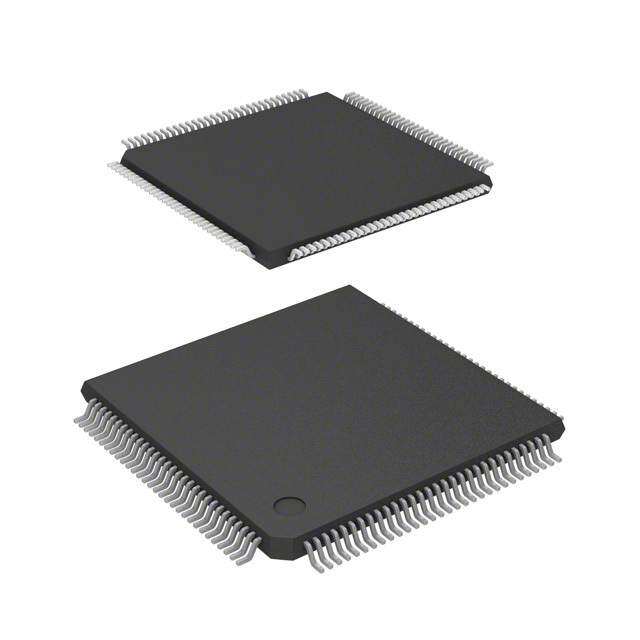
| 供应商器件封装 | 80-LQFP(12x12) |
| 其它名称 | M30280F8HP#U9 |
| 包装 | 托盘 |
| 外设 | DMA,POR,PWM,电压检测,WDT |
| 封装/外壳 | 80-LQFP |
| 工作温度 | -20°C ~ 85°C |
| 振荡器类型 | 内部 |
| 数据转换器 | A/D 24x10b |
| 标准包装 | 1 |
| 核心处理器 | M16C/60 |
| 核心尺寸 | 16-位 |
| 特色产品 | http://www.digikey.com/product-highlights/cn/zh/segger-microcontroller-systems-flasher-tools/3226 |
| 电压-电源(Vcc/Vdd) | 2.7 V ~ 5.5 V |
| 程序存储器类型 | 闪存 |
| 程序存储容量 | 64KB(64K x 8) |
| 连接性 | I²C, IEBus, SIO, UART/USART |
| 速度 | 20MHz |
| 配用 | /product-detail/zh/R0K330290S000BE/R0K330290S000BE-ND/1134900/product-detail/zh/M30290T2-CPE/M30290T2-CPE-ND/1134468 |


- 商务部:美国ITC正式对集成电路等产品启动337调查
- 曝三星4nm工艺存在良率问题 高通将骁龙8 Gen1或转产台积电
- 太阳诱电将投资9.5亿元在常州建新厂生产MLCC 预计2023年完工
- 英特尔发布欧洲新工厂建设计划 深化IDM 2.0 战略
- 台积电先进制程称霸业界 有大客户加持明年业绩稳了
- 达到5530亿美元!SIA预计今年全球半导体销售额将创下新高
- 英特尔拟将自动驾驶子公司Mobileye上市 估值或超500亿美元
- 三星加码芯片和SET,合并消费电子和移动部门,撤换高东真等 CEO
- 三星电子宣布重大人事变动 还合并消费电子和移动部门
- 海关总署:前11个月进口集成电路产品价值2.52万亿元 增长14.8%


PDF Datasheet 数据手册内容提取
To our customers, Old Company Name in Catalogs and Other Documents On April 1st, 2010, NEC Electronics Corporation merged with Renesas Technology Corporation, and Renesas Electronics Corporation took over all the business of both companies. Therefore, although the old company name remains in this document, it is a valid Renesas Electronics document. We appreciate your understanding. Renesas Electronics website: http://www.renesas.com April 1st, 2010 Renesas Electronics Corporation Issued by: Renesas Electronics Corporation (http://www.renesas.com) Send any inquiries to http://www.renesas.com/inquiry.
Notice 1. All information included in this document is current as of the date this document is issued. Such information, however, is subject to change without any prior notice. Before purchasing or using any Renesas Electronics products listed herein, please confirm the latest product information with a Renesas Electronics sales office. Also, please pay regular and careful attention to additional and different information to be disclosed by Renesas Electronics such as that disclosed through our website. 2. Renesas Electronics does not assume any liability for infringement of patents, copyrights, or other intellectual property rights of third parties by or arising from the use of Renesas Electronics products or technical information described in this document. No license, express, implied or otherwise, is granted hereby under any patents, copyrights or other intellectual property rights of Renesas Electronics or others. 3. You should not alter, modify, copy, or otherwise misappropriate any Renesas Electronics product, whether in whole or in part. 4. Descriptions of circuits, software and other related information in this document are provided only to illustrate the operation of semiconductor products and application examples. You are fully responsible for the incorporation of these circuits, software, and information in the design of your equipment. Renesas Electronics assumes no responsibility for any losses incurred by you or third parties arising from the use of these circuits, software, or information. 5. When exporting the products or technology described in this document, you should comply with the applicable export control laws and regulations and follow the procedures required by such laws and regulations. You should not use Renesas Electronics products or the technology described in this document for any purpose relating to military applications or use by the military, including but not limited to the development of weapons of mass destruction. Renesas Electronics products and technology may not be used for or incorporated into any products or systems whose manufacture, use, or sale is prohibited under any applicable domestic or foreign laws or regulations. 6. Renesas Electronics has used reasonable care in preparing the information included in this document, but Renesas Electronics does not warrant that such information is error free. Renesas Electronics assumes no liability whatsoever for any damages incurred by you resulting from errors in or omissions from the information included herein. 7. Renesas Electronics products are classified according to the following three quality grades: “Standard”, “High Quality”, and “Specific”. The recommended applications for each Renesas Electronics product depends on the product’s quality grade, as indicated below. You must check the quality grade of each Renesas Electronics product before using it in a particular application. You may not use any Renesas Electronics product for any application categorized as “Specific” without the prior written consent of Renesas Electronics. Further, you may not use any Renesas Electronics product for any application for which it is not intended without the prior written consent of Renesas Electronics. Renesas Electronics shall not be in any way liable for any damages or losses incurred by you or third parties arising from the use of any Renesas Electronics product for an application categorized as “Specific” or for which the product is not intended where you have failed to obtain the prior written consent of Renesas Electronics. The quality grade of each Renesas Electronics product is “Standard” unless otherwise expressly specified in a Renesas Electronics data sheets or data books, etc. “Standard”: Computers; office equipment; communications equipment; test and measurement equipment; audio and visual equipment; home electronic appliances; machine tools; personal electronic equipment; and industrial robots. “High Quality”: Transportation equipment (automobiles, trains, ships, etc.); traffic control systems; anti-disaster systems; anti- crime systems; safety equipment; and medical equipment not specifically designed for life support. “Specific”: Aircraft; aerospace equipment; submersible repeaters; nuclear reactor control systems; medical equipment or systems for life support (e.g. artificial life support devices or systems), surgical implantations, or healthcare intervention (e.g. excision, etc.), and any other applications or purposes that pose a direct threat to human life. 8. You should use the Renesas Electronics products described in this document within the range specified by Renesas Electronics, especially with respect to the maximum rating, operating supply voltage range, movement power voltage range, heat radiation characteristics, installation and other product characteristics. Renesas Electronics shall have no liability for malfunctions or damages arising out of the use of Renesas Electronics products beyond such specified ranges. 9. Although Renesas Electronics endeavors to improve the quality and reliability of its products, semiconductor products have specific characteristics such as the occurrence of failure at a certain rate and malfunctions under certain use conditions. Further, Renesas Electronics products are not subject to radiation resistance design. Please be sure to implement safety measures to guard them against the possibility of physical injury, and injury or damage caused by fire in the event of the failure of a Renesas Electronics product, such as safety design for hardware and software including but not limited to redundancy, fire control and malfunction prevention, appropriate treatment for aging degradation or any other appropriate measures. Because the evaluation of microcomputer software alone is very difficult, please evaluate the safety of the final products or system manufactured by you. 10. Please contact a Renesas Electronics sales office for details as to environmental matters such as the environmental compatibility of each Renesas Electronics product. Please use Renesas Electronics products in compliance with all applicable laws and regulations that regulate the inclusion or use of controlled substances, including without limitation, the EU RoHS Directive. Renesas Electronics assumes no liability for damages or losses occurring as a result of your noncompliance with applicable laws and regulations. 11. This document may not be reproduced or duplicated, in any form, in whole or in part, without prior written consent of Renesas Electronics. 12. Please contact a Renesas Electronics sales office if you have any questions regarding the information contained in this document or Renesas Electronics products, or if you have any other inquiries. (Note 1) “Renesas Electronics” as used in this document means Renesas Electronics Corporation and also includes its majority- owned subsidiaries. (Note 2) “Renesas Electronics product(s)” means any product developed or manufactured by or for Renesas Electronics.
M16C/28 Group (M16C/28, M16C/28B) REJ03B0201-0050 SINGLE-CHIP 16-BIT CMOS MCU Rev.0.50 2006.09.15 1. Overview The M16C/28 Group (M16C/28 and M16C/28B) MCU are single-chip control MCU, fabricated using high- performance silicon gate CMOS technology with the M16C/60 series CPU core. The M16C/28 Group (M16C/28 and M16C/28B) are housed in 64-pin and 80-pin plastic molded LQFP packages and also in 85- pin plastic molded TFLGA (Thin Fine Pitch Land Grid Array) package. With a 1-Mbyte address space, this MCU combines advanced instruction manipulation capabilities to process complex instructions by less bytes and execute instructions at higher speed. It includes a multiplier and DMAC adequate for office automation, communication devices and other high-speed processing applications. The M16C/28 has Normal-ver., T-ver., and V-ver.. The M16C/28B has Normal-ver. only. This hardware manual describes the Normal-ver. only. Please contact Renesas Technology Corp. for T-ver./V-ver. information. 1.1 Applications Audio, cameras, office equipment, communication equipment, portable equipment, home appliances (in- verter solution), motor control, industrial equipment, etc. Rev.0.50 Sep.15,2006 page 1 of33
M16C/28 Group (M16C/28, M16C/28B) 1. Overview 1.2 Performance Overview Table 1.1 and 1.2 outline performance overview of the M16C/28 Group (M16C/28, M16C/28B). Table 1.1 M16C/28 Group (M16C/28, M16C/28) Performance (80/85-Pin Package) Item Performance CPU Number of basic instructions 91 instructions Minimum instruction 41.7 ns (f(BCLK) = 24 MHZ, VCC = 4.2 V to 5.5 V) (M16C/28B) excution time 50 ns (f(BCLK) = 20 MHZ, VCC = 3.0 V to 5.5 V) (M16C/28, M16C/28B) 100 ns (f(BCLK) = 10 MHZ, VCC= 2.7 V to 5.5 V) (M16C/28, M16C/28B) Operation mode Single chip mode Address space 1M bytes Memory capacity See Table 1.3 Peripheral I/O port Input/Output : 71 lines Function Multifunction timer TimerA:16 bits x 5 channels, TimerB:16 bits x 3 channels Three-phase Motor Control Timer TimerS (Input Capture/Output Compare) : 16bit base timer x 1 channel (Input/Output x 8 channels) Serial I/O 2 channels (UART0, UART1) UART, clock synchronous 1 channel (UART2) UART, clock synchronous, I2C bus(1), or IEbus(2) 2 channels (SI/O3, SI/O4) Clock synchronous 1 channel (Multi-Master I2C bus(1)) A/D converter 10 bits x 24 channels DMAC 2 channels Watchdog timer 15 bits x 1 (with prescaler) Interrupt 25 internal and 8 external sources, 4 software sources, 7 levels Clock generation circuit 4 circuits • Main clock (*) • Sub-clock (*) • On-chip oscillator • PLL frequency synthesizer (*) Equipped with a built-in feedback resistor Oscillation Stop Detect Main clock oscillation stop, re-oscillation detect function Function Voltage detection circuit Available Electrical Power supply voltage VCC = 4.2 V to 5.5 V (f(BCLK) = 24 MHZ) (M16C/28B) Characteristics VCC = 3.0 V to 5.5 V (f(BCLK) = 20 MHZ) (M16C/28, M16C/28B) VCC = 2.7 V to 5.5 V (f(BCLK) = 10 MHZ) (M16C/28, M16C/28B) Power consumption 16 mA (VCC = 5V, f(BCLK) = 20 MHz) 25 µA (f(XCIN) = 32 KHz on RAM) 3.0 µA (VCC = 3V, f(XCIN) = 32 KHz, in wait mode) 0.7 µA (VCC = 3V, in stop mode) Flash Memory Program/erase supply voltage 2.7 V to 5.5 V Program and erase endurance 100 times (all space) or 1,000 times (Blocks 0 to 5) /10,000 times (Block A, Block B(3)) Operating Ambient Temperature -20 to 85°C/-40 to 85°C(3) Package 80-pin plastic mold LQFP, 85-pin plastic mold TFLGA NOTES: 1. I2C bus is a trademark of Koninklijke Philips Electronics N. V. 2. IEBus is a trademark of NEC Electronics Corporation. 3. Refer to Table 1.5 to 1.7 for number of program/erase. 4. Use PLL frequency synthesizer to use M16C/28B at f(BCLK) = 24 MHz. Rev.0.50 Sep.15,2006 page 2 of33
M16C/28Group(M16C/28,M16C/28B) 1. Overview Table 1.2 M16C/28 Group (M16C/28, M16C/28) (64-Pin Package) Item Performance CPU Number of basic instructions 91 instructions Minimum instruction 41.7 ns (f(BCLK) = 24 MHZ, VCC = 4.2 V to 5.5 V) (M16C/28B) excution time 50 ns (f(BCLK) = 20 MHZ, VCC = 3.0V to 5.5V) (M16C/28, M16C/28B) 100 ns (f(BCLK) = 10 MHZ, VCC = 2.7V to 5.5V) (M16C/28, M16C/28B) Operation mode Single chip mode Address space 1M bytes Memory capacity See Table 1.3 Peripheral I/O Port Input/Output : 55 lines Function Multifunction timer TimerA:16 bits x 5 channels, TimerB:16 bits x 3 channels Three-phase Motor Control Timer TimerS (Input Capture/Output Compare) : 16bit base timer x 1 channel (Input/Output x 8 channels ) Serial I/O 2 channels (UART0, UART1) UART, clock synchronous 1 channel (UART2) UART, clock synchronous, I2C bus(1), or IEbus(2) 1 channels (SI/O3, SI/O4) Clock synchronous 1 channel (Multi-Master I2C bus(1)) A/D converter 10 bits x 13 channels DMAC 2 channels Watchdog timer 15 bits x 1 (with prescaler) Interrupt 24 internal and 8 external sources, 4 software sources, 7 levels Clock generation circuit 4 circuits • Main clock(*) • Sub-clock(*) • On-chip oscillator • PLL frequency synthesizer (*) Equipped with a built-in feedback resistor Oscillation Stop Detect Main clock oscillation stop, re-oscillation detect function Function Voltage detection circuit Available Electrical Power supply voltage VCC = 4.2 V to 5.5 V (f(BCLK) = 24 MHZ) (M16C/28) Characteristics VCC = 3.0 V to 5.5 V (f(BCLK) = 20 MHZ) (M16C/28, M16C/28B) VCC = 2.7 V to 5.5 V (f(BCLK) = 10 MHZ) (M16C/28, M16C/28B) Power consumption 16 mA (VCC = 5 V, f(BCLK) = 20 MHz) 25 µA (f(XCIN) = 32 KHz on RAM) 3.0 µA (VCC = 3 V, f(XCIN) = 32 KHz, in wait mode) 0.7 µA (VCC = 3 V, in stop mode) Flash Memory Program/erase supply voltage 2.7 V to 5.5 V Program and erase endurance 100 times (all space) or 1,000 times (Blocks 0 to 5) /10,000 times (Block A, Block B(3)) Operating Ambient Temperature -20 to 85C°/-40 to 85C°(3) Package 64-pin plastic mold LQFP NOTES: 1. I2C bus is a trademark of Koninklijke Philips Electronics N. V. 2. IEBus is a trademark of NEC Electronics Corporation. 3. Refer to Table 1.5 to 1.7 for number of program/erase. 4. Use PLL frequency synthesizer to use M16C/28B at f(BCLK) = 24 MHz. Rev.0.50 Sep.15,2006 page 3 of33
M16C/28 Group (M16C/28, M16C/28B) 1. Overview 1.3 Block Diagram Figure 1.1 is a block diagram of the M16C/28 Group (M16C/28, M16C/28B), 80-pin and 85-pin package. Figure 1.2 is a block diagram of the M16C/28 Group (M16C/28, M16C/28B), 64-pin package. 8 8 8 8 I/O Ports Port P0 Port P1 Port P2 Port P3 P o Internal Peripheral Functions Prt 8 6 Timer (16 bits) UART/clock synchronous SI/O System clock generator (8 bits x 3 channels) Output (Timer A) : 5 XIN-XOUT P Input (Timer B) : 3 Cl(o8c kb istsy nxc 2h rcohnaonunse SlsI)/O OnX-cChINip- XoCsOciUllaTtor rt Po 8 3-phase PWM 7 Multi-master I2C bus PLL frequency synthesizer Timer S P ( Input capture/ ) o Time meOaustupruetm ceonmt p: a8r echannels M16C/60 Series CPU Core Memory P8rt 8 Waveform generating : 8 channels ROM(1) A/D converter R0H R0L SB Po (10 bits x 24 channels) R1HRR23 R1L UISSPP RAM(2) P9rt 7 INTB AAAA Watchdog timer A0 PC (15 bits) A1 P AAAA o DMAC FB FLG AAMuAltiplieAr 1rt P 8 (2 channels) 0 NOTES: 1. ROM size depends on MCU type. 2. RAM size depends on MCU type. Figure 1.1 M16C/28 Group (M16C/28, M16C/28B), 80-Pin/85-Pin Block Diagram Rev.0.50 Sep.15,2006 page 4 of33
M16C/28Group(M16C/28,M16C/28B) 1. Overview 4 3 8 4 I/O Ports Port P0 Port P1 Port P2 Port P3 P o Internal Peripheral Functions Prt 8 6 Timer (16 bits) UART/Clock synchronous SI/O System clock generator (8 bits x 3 channels) Output (Timer A) : 5 XIN-XOUT P Input (Timer B) : 3 Clo(8ck b sitysn xc h1r ochnaonuns eSl)I/O OnX-cChINip- XoCsOciUllaTtor rt Po 8 3-phase PWM 7 Multi-master I2C bus PLL frequency synthesizer Timer S P ( Input capture/ ) o Time meOaustupruetm ceonmt p: a8r echannels M16C/60 Series CPU Core Memory 8rt P 8 Waveform generating : 8 channels ROM(1) (10 Abi/tsD xc 1o3n cvhearntenrels) RR01HHRR23 RR01LL SUIBSSPP RAM(2) P9rt Po 4 INTB Watchdog timer A0 AAAA PC (15 bits) A1 P FB FLG AAAA o DMAC Multiplier rt P 8 (2 channels) 1 0 NOTES: 1. ROM size depends on MCU type. 2. RAM size depends on MCU type. Figure 1.2 M16C/28 Group (M16C/28, M16C/28B), 64-Pin Block Diagram Rev.0.50 Sep.15,2006 page 5 of33
M16C/28 Group (M16C/28, M16C/28B) 1. Overview 1.4 Product Information Tables 1.3 and 1.4 list the M16C/28 Group product information and Figure 1.3 shows the product number- ing system. The specifications are partially different between normal-ver.and T/ V-ver.. Table 1.3 M16C/28 Product List -Normal-ver. As of September, 2006 ROM RAM TypeNumber PackageType Remarks ProductCode Capacity Capacity M30280F6WG (N) 48K+4K 4K M30280F8WG (N) 64K+4K 4K PTLG0085JB-A(85F0G) M30280FAWG (N) 96K+4K 8K M30280F6HP (N) 48K+4K 4K M30280F8HP (N) 64K+4K 4K PLQP0080KB-A(80P6Q-A) Flash M30280FAHP (N) 96K+4K 8K U3,U5,U7,U9 Memory M30280FCHP (N) 128K+4K 12K M30281F6HP (N) 48K+4K 4K M30281F8HP (N) 64K+4K 4K PLQP0064KB-A(64P6Q-A) M30281FAHP (N) 96K+4K 8K M30281FCHP (N) 128K+4K 12K M30280M8-XXXHP (N) 64K 4K M30280MA-XXXHP (N) 96K 8K PLQP0080KB-A(80P6Q-A) M30280MC-XXXHP (N) 128K 12K Mask U3,U5 ROM M30281M8-XXXHP (N) 64K 4K M30281MA-XXXHP (N) 96K 8K PLQP0064KB-A(64P6Q-A) M30281MC-XXXHP (N) 128K 12K (N): New Table 1.4 M16C/28B Product List -Normal-ver. As of September, 2006 ROM RAM TypeNumber PackageType Remarks ProductCode Capacity Capacity M30280FCBHP (D) 128K+4K 12K PLQP0080KB-A(80P6Q-A) Flash U7 M30281FCBHP (D) 128K+4K 12K PLQP0064KB-A(64P6Q-A) memory (D):Underdevelopment Rev.0.50 Sep.15,2006 page 6 of33
M16C/28Group(M16C/28,M16C/28B) 1. Overview Type No. M 3 0 2 8 0 F C B H P - U 7 Product code Package type: HP : Package PLQP0080KB-A(80P6Q-A) PLQP0064KB-A(64P6Q-A) WG: Package PTLG0085JB-A(85F0G) Version (no): M16C/28 Group Normal-ver. B: M16C/28B Group ROM capacity / RAM capacity (1): 6 : (48K+4K) bytes / 4K bytes 8 : (64K + 4K) bytes / 4K bytes A: (96K + 4K) bytes / 8K bytes C: (128K + 4K) bytes / 12K bytes Memory type: F : Flash memory version M: Mask ROM version Pin count (The value itself has no specific meaning) M16C/28 Group, M16C/28B Group M16C Family NOTE: 1. "+4K bytes" is available only in flash memory ver.. Figure 1.3 Product Numbering System Rev.0.50 Sep.15,2006 page 7 of33
M16C/28 Group (M16C/28, M16C/28B) 1. Overview Table 1.5 Product Code (Flash Memory-ver.) - M16C/28 Normal-ver., 64-Pin(1)/80-Pin(1)/85-Pin Package InternalROM InternalROM (UserProgramSpace) (DataSpace) Product OperatingAmbient Package Code Programand Programand Temperature Temperature Temperature Erase Erase Range Range Endurance Endurance U3 -40to85ºC 100 100 0to60ºC U5 -20to85ºC Leadfree 0to60ºC U7 -40to85ºC -40to85ºC 1,000 10,000 U9 -20to85ºC -20to85ºC NOTE: 1. The lead contained products, D3, D5, D7 and D9, are put together with U3, U5, U7 and U9 respectively. Lead- free (Sn-Ag-Cu plating) products can be mounted by both conventional Sn-Pb paste and Lead-free paste. Table 1.6 Product Code (Flash Memory-ver.) - M16C/28B Normal-ver., 64-Pin/85-Pin Package InternalROM InternalROM (UserProgramSpace) (DataSpace) Product OperatingAmbient Package Code Program Program Temperature Temperature Temperature andErase andErase Range Range Endurance Endurance U7 Lead-free 1,000 0to60ºC 10,000 -40to85ºC -40to85ºC Table 1.7 Product Code (Mask ROM ver.) - M16C/28B Normal-ver., 64-Pin/80-Pin/85-Pin Package Product OperatingAmbient Package Code Temperature U3 -40to85ºC Lead-free U5 -20to85ºC Rev.0.50 Sep.15,2006 page 8 of33
M16C/28Group(M16C/28,M16C/28B) 1. Overview (1) Flash Memory Version, PTLG0085JB-A (85F0G), Normal-ver. M30280FA Type No. M30280FAWG B U5 Chip version and product code XXXXXXX B : Chip version. The first edition is shown to be blank and continues with A, B, and C. U5: Product code. (See Table 1.5) Date code seven digits Manufacturing management code (2) Flash Memory Version, PLQP0080KB-A (80P6Q-A), Normal-ver. M16C M30280FAHP Type No. M30280FAHP A U5 Chip version and product code XXXXXXX A : Chip version and product code(1) The first edition is shown to be blank and continues with A, B and C. U5 : Product code. (Table 1.4) Date code seven digits Manufacturing management code (3) Flash Memory Version, PLQP0064KB-A (64P6Q-A), Normal-ver. 30281FA Type No. M30281FAHP A U5 Chip version and product code (1) A : Chip version and product code XXXXXXX The first edition is shown to be blank and continues with A, B and C. U5 : Product code. (Table 1.4) Date code seven digits Manufacturing management code (4) Mask ROM Version, PLQP0080KB-A (80P6Q-A), Normal-ver. M16C Type No. M30280MAHP M30280MA- XXXHP A U5 Chip version and product code XXXXXXX XXX : ROM No. (1) A : Chip version and product code The first edition is shown to be blank and continues with A, B and C. U5 : Product code. (Table 1.6) Date code seven digits Manufacturing management code (5) Mask ROM Version, PLQP0064-KB-A (64P6Q-A), Normal-ver. Date code seven digits XXXXXXX Manufacturing management code M30281MA- Type No. M30281MAHP XXXHP A U5 Chip version and product code XXX: ROM No. (1) A : Chip version and product code The first edition is shown to be blank and continues with A, B and C. U5 : Product code. (Table 1.6) NOTES: 1. The following functinos are not available in the first version and version A products. -Delay trigger mode 0 of A/D conversion -Delay trigger mode 1 of A/D conversion Figure 1.4 Marking Diagram-M16C/28 Normal-ver. Rev.0.50 Sep.15,2006 page 9 of33
M16C/28 Group (M16C/28, M16C/28B) 1. Overview 1.5 Pin Assignment Figures 1.5 to 1.7 show the pin Assignments (top view). A B C D E F G H J K 10 61 60 58 5 52 50 47 44 42 38 P06 P07 P11 P14 P17 P21 P24 P27 P61 P31 9 62 63 59 5 53 51 48 45 43 39 P05 P04 P10 P13 P16 P20 P23 P26 P60 P30 8 64 65 66 5 54 (11) 49 46 41 40 P03 P02 P01 P12 P15 (Vss)(2) P22 P25 P62 P63 7 67 68 69 37 36 35 P00 P107 P106 P32 P33 P34 6 70 71 (11) 34 33 32 P105 P104 (Vss)(2) P35 P36 P37 5 74 73 72 (11) 31 30 P101 P102 P103 (Vss)(2) P64 P65 4 77 76 75 (11) 29 28 27 VREF P100 AVss (Vss)(2) P66 P67 P70 3 78 79 4 9 11 14 17 26 25 24 AVcc P97 P91 RESET Vss P85 P82 P71 P72 P73 2 80 2 5 7 12 13 16 19 23 22 P96 P93 P90 P87/XCIN XIN Vcc P83 P80 P74 P75 1 1 3 6 8 10 13 15 18 21 20 P95 P92 CNVss P86/XCOUT XOUT Vcc P84 P81 P76 P77 NOTES : 1. The numbers in each grid (circle) show the pin numbers of the M30280FAHP (80P6Q-A package) 2. Connect grids written as (Vss) to Vss(GND) or leave them open. 3. Set PACR2 to PACR0 bits in the PACR register to "0112" before you input and output it after resetting to each pin. When the PACR register is not set, the input and output function of some pins are disabled. Package: PTLG0085JB-A(85F0G) Figure 1.5 Pin Assignment (Top View) of 85-pin Package Rev.0.50 Sep.15,2006 page 10 of33
M16C/28Group(M16C/28,M16C/28B) 1. Overview Table 1.8 Pin Characteristics for 85-pin Package Pin Control Interrupt Multi-master PLQP0080KB-A Port TimerPin TimerSPin UARTPin AnalogPin No. Pin Pin I2CbusPin PinNumber A1 P95 CLK4 AN25 1 A2 P96 SOUT4 AN26 80 A3 AVcc 78 A4 VREF 77 A5 P101 AN1 74 A6 P105 KI1 AN5 70 A7 P00 AN00 67 A8 P03 AN03 64 A9 P05 AN05 62 A10 P06 AN06 61 B1 P92 TB2IN 3 B2 P93 AN24 2 B3 P97 SIN4 AN27 79 B4 P100 AN0 76 B5 P102 AN2 73 B6 P104 KI0 AN4 71 B7 P107 KI3 AN7 68 B8 P02 AN02 65 B9 P04 AN04 63 B10 P07 AN07 60 C1 CNVss 6 C2 P90 TB0IN 5 C3 P91 TB1IN 4 C4 AVss 75 C5 P103 AN3 72 C6 Vss(1) (11) C7 P106 KI2 AN6 69 C8 P01 AN01 66 C9 P10 AN20 59 C10 P11 AN21 58 P86 D1 XCOUT 8 D2 XCIN P87 7 D3 RESET 9 D4 Vss(1) (11) D8 P12 AN22 57 D9 P13 AN23 56 D10 P14 55 E1 XOUT 10 E2 XIN 12 E3 Vss 11 Rev.0.50 Sep.15,2006 page 11 of33
M16C/28 Group (M16C/28, M16C/28B) 1. Overview Table 1.8 Pin Characteristics for 85-pin Package (continued) Pin Control Interrupt Multi-master PLQP0080KB-A Port TimerPin TimerSPin UARTPin AnalogPin No. Pin Pin I2CbusPin PinNumber E8 P15 INT3 IDV ADTRG 54 E9 P16 INT4 IDW 53 E10 P17 INT5 IDU INPC17 52 F1 Vcc 13 F2 Vcc 13 F3 P85 NMI SD 14 F8 Vss(1) (11) OUTC10/ F9 P20 INPC10 SDAMM 51 OUTC11/ F10 P21 INPC11 SCLMM 50 G1 P84 INT2 ZP 15 G2 P83 INT1 16 G3 P82 INT0 17 OUTC12/ G8 P22 INPC12 49 OUTC13/ G9 P23 INPC13 48 OUTC14/ G10 P24 INPC14 47 H1 P81 TA4IN/U 18 H2 P80 TA4OUT/U 19 H3 P71 TA0IN RXD2/SCL2/CLK1 26 H4 P66 RXD1 29 H5 Vss(1) (11) H6 P35 34 H7 P32 SOUT3 37 OUTC15/ H8 P25 INPC15 46 OUTC16/ H9 P26 INPC16 45 OUTC17/ H10 P27 INPC17 44 J1 P76 TA3OUT 21 J2 P74 TA2OUT/W 23 J3 P72 TA1OUT/V CLK2/RXD1 25 J4 P67 TXD1 28 RTS1/CTS1/CTS0/ J5 P64 CLKS1 31 J6 P36 33 J7 P33 36 J8 P62 RXD0 41 J9 P60 RTS0/CTS0 43 J10 P61 CLK0 42 K1 P77 TA3IN 20 K2 P75 TA2IN/W 22 K3 P73 TA1IN/V CTS2/RTS2/TXD1 24 TXD2/SDA2/ RTS1/ K4 P70 TA0OUT CTS1/CTS0/CLKS1 27 K5 P65 CLK1 30 K6 P37 32 K7 P34 35 K8 P63 TXD0 40 K9 P30 CLK3 39 K10 P31 SIN3 38 Rev.0.50 Sep.15,2006 page 12 of33
M16C/28Group(M16C/28,M16C/28B) 1. Overview M M M M A L D C S S P0/AN077 P1/AN200 P1/AN211 P1/AN222P1/AN233 P14 P1/INT/AD/IDV53TRG P1/INT/IDW64 P1/INT/INPC1/IDU757 P2/OUTC1/INPC1/000 P2/OUTC1/INPC1/111 P2/OUTC1/INPC1222 P2/OUTC1/INPC1333 P2/OUTC1/INPC1444 P2/OUTC1/INPC1555 P2/OUTC1/INPC1666 P2/OUTC1/INPC1777 P6/CTS/RTS000 P6/CLK10 P6/RxD20 6059 58 57 56 55 54 53 52 51 50 49 48 47 46 45 44 43 42 41 P06/AN06 61 40 P63/TXD0 P05/AN05 62 39 P30/CLK3 P04/AN04 63 38 P31/SIN3 P03/AN03 64 37 P32/SOUT3 P02/AN02 65 36 P33 P01/AN01 66 35 P34 P00/AN00 67 34 P35 P107/AN7/KI3 68 33 P36 P106/AN6/KI2 69 32 P37 P105/AN5/KI1 70 31 P64/CTS1/RTS1/CTS0/CLKS1 P104/AN4/KI0 71 30 P65/CLK1 P103/AN3 72 29 P66/RxD1 P102/AN2 73 28 P67/TXD1 P101/AN1 74 27 P70/TXD2/SDA2/TA0OUT/CTS1/RTS1/CTS0/CLKS1 AVSS 75 26 P71/RXD2/SCL2/TA0IN/CLK1 P100/AN0 76 25 P72/CLK2/TA1OUT/V/RxD1 VREF 77 24 P73/CTS2/RTS2/TA1IN/V/TxD1 AVcc 78 23 P74/TA2OUT/W P97/AN27/SIN4 79 22 P75/TA2IN/W P96/AN26/SOUT4 80 21 P76/TA3OUT 1 2 3 4 5 6 7 8 9 10 1112 13 14 15 16 17 18 19 20 P9/AN2/CLK554 P9/AN234 P9/TB22IN P9/TB11IN P9/TB00INCNVssP8/X7CINP8/X6COUT RESETXOUT VSS XIN VCC P8/NMI/SD5 P8/INT/ZP42 P8/INT31 P8/INT20 P8/TA4/U1IN P8/TA4/U0OUT P7/TA37IN NOTES: 1.Set PACR2 to PACR0 bit in the PACR register to "0112" before you input and output it after resetting to each pin. When the PACR register isn't set up, the input and output function of some of the pins are disabled. Package: PLQP0080KB-A(80P6Q-A) Figure 1.5 Pin Assignment (Top View) of 80-Pin Package Rev.0.50 Sep.15,2006 page 13 of33
M16C/28 Group (M16C/28, M16C/28B) 1. Overview Table 1.9 Pin Characteristics for 80-Pin Package Pin Control Interrupt Multi-master Port TimerPin TimerSPin UARTPin AnalogPin No. Pin Pin I2CbusPin 1 P95 CLK4 AN25 2 P93 AN24 3 P92 TB2IN 4 P91 TB1IN 5 P90 TB0IN 6 CNVss 7 XCIN P87 8 XCOUT P86 9 RESET 10 XOUT 11 Vss 12 XIN 13 Vcc 14 P85 NMI SD 15 P84 INT2 ZP 16 P83 INT1 17 P82 INT0 18 P81 TA4IN/U 19 P80 TA4OUT/U 20 P77 TA3IN 21 P76 TA3OUT 22 P75 TA2IN/W 23 P74 TA2OUT/W 24 P73 TA1IN/V CTS2/RTS2/TXD1 25 P72 TA1OUT/V CLK2/RXD1 26 P71 TA0IN RXD2/SCL2/CLK1 TXD2/SDA2/ RTS1/ 27 P70 TA0OUT CTS1/CTS0/CLKS1 28 P67 TXD1 29 P66 RXD1 30 P65 CLK1 RTS1/CTS1/CTS0/ 31 P64 CLKS1 32 P37 33 P36 34 P35 35 P34 36 P33 37 P32 SOUT3 38 P31 SIN3 39 P30 CLK3 40 P63 TXD0 Rev.0.50 Sep.15,2006 page 14 of33
M16C/28Group(M16C/28,M16C/28B) 1. Overview Table 1.9 Pin Characteristics for 80-Pin Package (Continued) Pin Control Interrupt Multi-master Port TimerPin TimerSPin UARTPin AnalogPin No. Pin Pin I2CbusPin 41 P62 RXD0 42 P61 CLK0 43 P60 RTS0/CTS0 44 P27 OUTC17/INPC17 45 P26 OUTC16/INPC16 46 P25 OUTC15/INPC15 47 P24 OUTC14/INPC14 48 P23 OUTC13/INPC13 49 P22 OUTC12/INPC12 50 P21 OUTC11/INPC11 SCLMM 51 P20 OUTC10/INPC10 SDAMM 52 P17 INT5 IDU INPC17 53 P16 INT4 IDW 54 P15 INT3 IDV ADTRG 55 P14 56 P13 AN23 57 P12 AN22 58 P11 AN21 59 P10 AN20 60 P07 AN07 61 P06 AN06 62 P05 AN05 63 P04 AN04 64 P03 AN03 65 P02 AN02 66 P01 AN01 67 P00 AN00 68 P107 KI3 AN7 69 P106 KI2 AN6 70 P105 KI1 AN5 71 P104 KI0 AN4 72 P103 AN3 73 P102 AN2 74 P101 AN1 75 AVss 76 P100 AN0 77 VREF 78 AVcc 79 P97 SIN4 AN27 80 P96 SOUT4 AN26 Rev.0.50 Sep.15,2006 page 15 of33
M16C/28 Group (M16C/28, M16C/28B) 1. Overview M M M M A L D C S S P0/AN033 P1/INT/AD/IDV53TRG P1/INT/IDW64 P1/INT/INPC1/IDU757 P2/OUTC1/INPC1/000 P2/OUTC1/INPC1/111 P2/OUTC1/INPC1222 P2/OUTC1/INPC1333 P2/OUTC1/INPC1444 P2/OUTC1/INPC1555 P2/OUTC1/INPC1666 P2/OUTC1/INPC1777 P6/CTS/RTS000 P6/CLK10 P6/RxD20 P6/TxD30 8 7 6 5 4 3 2 1 0 9 8 7 6 5 4 3 4 4 4 4 4 4 4 4 4 3 3 3 3 3 3 3 P02/AN02 49 32 P30/CLK3 P01/AN01 50 31 P31/SIN3 P00/AN00 51 30 P32/SOUT3 P107/AN7/KI3 52 29 P33 P106/AN6/KI2 53 28 P64/CTS1/RTS1/CTS0/CLKS1 P105/AN5/KI1 54 27 P65/CLK1 P104/AN4/KI0 55 26 P66/RxD1 P103/AN3 56 25 P67/TxD1 P102/AN2 57 24 P70/TxD2/SDA2/TA0OUT/RTS1/CTS1/CTS0/CLKS1 P101/AN1 58 23 P71/RxD2/SCL2/TA0IN/CLK1 AVSS 59 22 P72/CLK2/TA1OUT/V/RxD1 P100/AN0 60 21 P73/CTS2/RTS2/TA1IN/V/TxD1 VREF 61 20 P74/TA2OUT/W AVCC 62 19 P75/TA2IN/W P93/AN24 63 18 P76/TA3OUT P92/TB2IN 64 17 P77/TA3IN 1 2 3 4 5 6 7 8 9 10 11 12 13 14 15 16 P9/TB11IN P9/TB00IN CNVSS P8/X7CIN P8/XCOUT6 RESET XOUT VSS XIN VCC P8/NMI/SD5 P8/INT/ZP42 P8/INT31 P8/INT20 P8/TA4/U1IN 8/TA4/U0OUT P NOTES: 1.Set PACR2 to PACR0 bit in the PACR register to "0102" before you input and output it after resetting to each pin. When the PACR register isn't set up, the input and output function of some of the pins are disabled. Package: PLQP0064KB-A(64P6Q-A) Figure 1.6 Pin Assignment (Top View) of 64-Pin Package Rev.0.50 Sep.15,2006 page 16 of33
M16C/28Group(M16C/28,M16C/28B) 1. Overview Table 1.10 Pin Characteristics for 64-Pin Package Pin Control Interrupt Mult-master Port TimerPin TimerSPin UARTPin AnalogPin No. Pin Pin I2CbusPin 1 P91 TA1IN 2 P90 TB0IN 3 CNVss 4 XCIN P87 5 XCOUT P86 6 RESET 7 XOUT 8 Vss 9 XIN 10 Vcc 11 P85 NMI SD 12 P84 INT2 ZP 13 P83 INT1 14 P82 INT0 15 P81 TA4IN/U 16 P80 TA4OUT/U 17 P77 TA3IN 18 P76 TA3OUT 19 P75 TA2IN/W 20 P74 TA2OUT/W 21 P73 TA1IN/V CTS2/RTS2/TXD1 22 P72 TA1OUT/V CLK2/RXD1 23 P71 TA0IN RXD2/SCL2/CLK1 TXD2/SDA2/ RTS1/ 24 P70 TA0OUT CTS1/CTS0/CLKS1 25 P67 TXD1 26 P66 RXD1 27 P65 CLK1 RTS1/CTS1/CTS0/ 28 P64 CLKS1 29 P33 30 P32 SOUT3 31 P31 SIN3 32 P30 CLK3 33 P63 TXD0 34 P62 RXD0 35 P61 CLK0 36 P60 RTS0/CTS0 37 P27 OUTC17/INPC17 38 P26 OUTC16/INPC16 39 P25 OUTC15/INPC15 40 P24 OUTC14/INPC14 Rev.0.50 Sep.15,2006 page 17 of33
M16C/28 Group (M16C/28, M16C/28B) 1. Overview Table 10 Pin Characteristics for 64-Pin Package (Continued) Pin Control Interrupt Multi-master Port TimerPin TimerSPin UARTPin AnalogPin No. Pin Pin I2CbusPin 41 P23 OUTC13/INPC13 42 P22 OUTC12/INPC12 43 P21 OUTC11/INPC11 SCLMM 44 P20 OUTC10/INPC10 SDAMM 45 P17 INT5 IDU INPC17 46 P16 INT4 IDW 47 P15 INT3 IDV ADTRG 48 P03 AN03 49 P02 AN02 50 P01 AN01 51 P00 AN00 52 P107 KI3 AN7 53 P106 KI2 AN6 54 P105 KI1 AN5 55 P104 KI0 AN4 56 P103 AN3 57 P102 AN2 58 P101 AN1 59 AVss 60 P100 AN0 61 VREF 62 AVcc 63 P93 AN24 64 P92 TB2IN Rev.0.50 Sep.15,2006 page 18 of33
M16C/28Group(M16C/28,M16C/28B) 1. Overview 1.6 Pin Description Table 1.10 Pin Description (64-Pin, 80-Pin and 85-Pin Packages) Classification Symbol I/O Type Function Power Supply VCC, VSS I Apply 2.7 to 5.5V to the Vcc pin. Apply 0V to the Vss pin. Analog Power AVCC I Supplies power to the A/D converter. Connect the AVCC pin to VCC and Supply AVSS the AVSS pin to VSS. ____________ ___________ Reset Input RESET I The MCU is in a reset state when "L" is applied to the RESET pin CNVSS CNVSS I Connect the CNVSS pin to VSS. Main Clock I/O pins for the main clock oscillation circuit. Connect a ceramic resonator XIN I Input or crystal oscillator between XIN and XOUT. To apply external clock, apply Main Clock XOUT O it to XIN and leave XOUT open. If XIN is not used (for external oscillator or Output external clock) connect XIN pin to VCC and leave XOUT open. Sub Clock Input XCIN I I/O pins for the sub clock oscillation circuit. Connect a crystal oscillator Sub Clock Output XCOUT O between XCIN and XCOUT. ______ ________ ________ ______ ________ INT Interrupt INT0 to INT5 I Input pins for the INT interrupt. INT2 can be used for Timer A Z-phase Input function. _______ _______ _______ _______ NMI Interrupt NMI I Input pin for the NMI interrupt. NMI cannot be used as I/O port while the three- _______ Input phase motor control is enabled. Apply a stable "H" to NMI after setting it's direction register to "0" when the three-phase motor control is enabled. _____ _____ Key Input Interrupt KI0 to KI3 I Input pins for the key input interrupt Timer A TA0OUT to I/O I/O pins for the timer A0 to A4 TA4OUT TA0IN to I Input pins for the timer A0 to A4 TA4IN ZP I Input pin for Z-phase Timer B TB0IN to I Input pins for the timer B0 to B2 TB2IN ___ ___ Three-phase U, U, V, V, O Output pins for the three-phase motor control timer ___ Motor Control W, W Timer Output IDU, IDW, I/O Input and output pins for the three-phase motor control timer _____ IDV, SD _________ _________ Serial I/O CTS0 to CTS2 I Input pins for data transmission control _________ _________ RTS0 to RTS2 O Output pins for data reception control CLK0 to CLK3 I/O Inputs and outputs the transfer clock RxD0 to RxD2 I Inputs serial data TxD0 to TxD2 O Outputs serial data CLKS1 O Output pin for transfer clock I2C Mode SDA2 I/O Inputs and outputs serial data SCL2 Inputs and outputs the transfer clock Multi-master SDAMM I/O Inputs and outputs serial data I2C bus SCLMM Inputs and outputs the transfer clock Reference VREF I Applies reference voltage to the A/D converter Voltage Input A/D Converter AN0 to AN7 I Analog input pins for the A/D converter AN00 to AN03 AN24 ___________ ADTRG Input pin for an external A/D trigger I : Input O : Output I/O : Input and output Rev.0.50 Sep.15,2006 page 19 of33
M16C/28 Group (M16C/28, M16C/28B) 1. Overview Table 1.10 Pin Description (64-Pin, 80-Pin and 85-Pin Packages) (Continued) Classification Symbol I/O Type Function Timer S INPC10 to INPC17 I Input pins for the time measurement function OUTC10 to OUTC17 O Output pins for the waveform generating function I/O Ports P00 to P03 I/O I/O ports for CMOS. Each port can be programmed for input or output P15 to P17 under the control of the direction register. An input port can be set, by P20 to P27 program, for a pull-up resistor available or for no pull-up resister available P30 to P33 in 4-bit units P60 to P67 P70 to P77 P80 to P87 P100 to P107 P90 to P93 I/O I/O ports having equivalent functions to P0 I : Input O : Output I/O : Input and output Rev.0.50 Sep.15,2006 page 20 of33
M16C/28Group(M16C/28,M16C/28B) 1. Overview Table 1.10 Pin Description (80-Pin and 85-Pin Packages only) (Continued) Classification Symbol I/O Type Function Serial I/O CLK4 I/O Inputs and outputs the transfer clock SIN4 I Inputs serial data SOUT4 O Outputs serial data A/D Converter AN04 to AN07 I Analog input pins for the A/D converter AN20 to AN23 AN25 to AN27 I/O Ports P04 to P07 I/O I/O ports for CMOS. Each port can be programmed for input or output under the P10 to P14 control of the direction register. An input port can be set, by program, for a pull- P34 to P37 up resistor available or for no pull-up resister available in 4-bit units P95 to P97 I/O I/O ports having equivalent functions to P0 I : Input O : Output I/O : Input and output Rev.0.50 Sep.15,2006 page 21 of33
M16C/28 Group (M16C/28, M16C/28B) 2. Central Processing Unit(CPU) 2. Central Processing Unit (CPU) Figure 2.1 shows the CPU registers. The register bank is comprised of 7 registers (R0, R1, R2, R3, A0, A1 and FB) out of 13 CPU registers. Two sets of register banks are provided. b31 b15 b8 b 7 b0 R2 R0H(R0's high bits) R0L(R0's low bits) R3 R1H(R1's high bits) R1L(R1's low bits) (1) Data registers R2 R3 A0 (1) A1 Address registers FB (1) Frame base registers b19 b15 b0 INTBH INTBL Interrupt table register The upper 4 bits of INTB are INTBH and the lower 16 bits of INTB are INTBL. b19 b0 PC Program counter b15 b0 USP User stack pointer ISP Interrupt stack pointer SB Static base register b15 b0 FLG Flag register b15 b8 bb7 b0 Carry flag Debug flag Zero flag Sign flag Register bank select flag Overflow flag Interrupt enable flag Stack pointer select flag Reserved space Processor interrupt priority level Reserved space NOTES: 1. The register bank is comprised of these registers. Two sets of register banks are provided. Figure 2.1 Central Processing Unit Register 2.1 Data Registers (R0, R1, R2 and R3) The R0, R1, R2 and R3 registers are 16 bit registers for transfer and arithmetic/logic operations. The R0 and R1 registers can be split into high-order bits(R0H, R1H) and low-order bits (R0L, R1L) to be used seperately as 8-bit data registers. Conversely, R2 and R0 can be combined with R2 to be used as a 32-bit data register (R2R0). The same applies to R1 and R2. 2.2 Address Registers (A0 and A1) The register A0 consists of 16 bits, and is used for address register indirect addressing and address register relative addressing. They also are used for transfers and arithmetic/logic operations. A1 is the same as A0. In some instructions, registers A1 and A0 can be combined for use as a 32-bit address register (A1A0). Rev.0.50 Sep.15,2006 page 22 of33
M16C/28Group(M16C/28,M16C/28B) 2. Central Processing Unit(CPU) 2.3 Frame Base Register (FB) FB is configured with 16 bits, and is used for FB relative addressing. 2.4 Interrupt Table Register (INTB) INTB is configured with 20 bits, indicating the start address of an interrupt vector table. 2.5 Program Counter (PC) PC is configured with 20 bits, indicating the address of an instruction to be executed. 2.6 User Stack Pointer (USP) and Interrupt Stack Pointer (ISP) Stack pointer (SP) comes in two types: USP and ISP, each configured with 16 bits. Your desired type of stack pointer (USP or ISP) can be selected by the U flag of FLG. 2.7 Static Base Register (SB) SB is configured with 16 bits, and is used for SB relative addressing. 2.8 Flag Register (FLG) FLG consists of 11 bits, indicating the CPU status. 2.8.1 Carry Flag (C Flag) This flag retains a carry, borrow, or shift-out bit that has occurred in the arithmetic/logic unit. 2.8.2 Debug Flag (D Flag) The D flag is used exclusively for debugging purpose. During normal use, it must be set to 0. 2.8.3 Zero Flag (Z Flag) This flag is set to 1 when an arithmetic operation resulted in 0; otherwise, it is 0. 2.8.4 Sign Flag (S Flag) This flag is set to 1 when an arithmetic operation resulted in a negative value; otherwise, it is 0. 2.8.5 Register Bank Select Flag (B Flag) Register bank 0 is selected when this flag is 0 ; register bank 1 is selected when this flag is 1. 2.8.6 Overflow Flag (O Flag) This flag is set to 1 when the operation resulted in an overflow; otherwise, it is 0. 2.8.7 Interrupt Enable Flag (I Flag) This flag enables a maskable interrupt. Maskable interrupts are disabled when the I flag is 0, and are enabled when the I flag is 1. The I flag is cleared to 0 when the interrupt request is accepted. 2.8.8 Stack Pointer Select Flag (U Flag) ISP is selected when the U flag is 0; USP is selected when the U flag is 1. The U flag is cleared to 0 when a hardware interrupt request is accepted or an INT instruction for software interrupt Nos. 0 to 31 is executed. 2.8.9 Processor Interrupt Priority Level (IPL) IPL is configured with three bits, for specification of up to eight processor interrupt priority levels from level 0 to level 7. If a requested interrupt has priority greater than IPL, the interrupt is enabled. 2.8.10 Reserved Area When write to this bit, write 0. When read, its content is indeterminate. Rev.0.50 Sep.15,2006 page 23 of33
M16C/28 Group (M16C/28, M16C/28B) 3. Memory 3. Memory Figure 3.1 is a memory map of the M16C/28 Group (M16C/28, M16C/28B). M16C/28 Group provides 1- Mbyte address space from addresses 0000016 to FFFFF16. The internal ROM is allocated lower addresses beginning with address FFFFF16. For example, 64 Kbytes internal ROM is allocated addresses F000016 to FFFFF16. Two 2-Kbyte internal ROM areas, block A and block B, are available in the flash memory version. The blocks are allocated addresses F00016 to FFFF16. The fixed interrupt vector tables are allocated addresses FFFDC16 to FFFFF16. It stores the starting ad- dress of each interrupt routine. See the section on interrupts for details. The internal RAM is allocated higher addresses beginning with address 0040016. For example, 4-Kbytes internal RAM is allocated addresses 0040016 to 013FF16. Besides storing data, it becomes stacks when the subroutine is called or an interrupt is acknowledged. SFR, consisting of control registers for peripheral functions such as I/O port, A/D converter, serial I/O, timers is allocated addresses 0000016 to 003FF16. All blank spaces within SFR are reserved and cannot be accessed by users. The special page vector table is allocated to the addresses FFE0016 to FFFDB16. This vector is used by the JMPS or JSRS instruction. For details, refer to the M16C/60 and M16C/20 Series Software Manual. Internal RAM area Internal ROM area Memory size XXXXX16 Memory size YYYYY16 4K bytes 013FF16 48K bytes F400016 6K bytes 01AFF16 64K bytes F000016 0000016 8K bytes 023FF16 96K bytes E800016 SFR Area 12K bytes 033FF16 128K bytes E000016 0040016 Internal RAM Area FFE0016 XXXXX16 RESERVED S p e c ia l P a g e 0F00016 Vector Table Internal ROM Area (data space)(1) 0FFFF16 FFFDC16 Undefined Instruction Overflow RESERVED BRK Instruction Address Match Single Step YYYYY16 Watchdog Timer DBC Internal ROM Area (program space) NMI FFFFF16 F F F F F 1 6 Reset NOTES: 1. The block A (2K bytes) and block B (2K bytes) are shown (only flash memory). 2. Do not write to the internal ROM area in Mask ROM ver.. Figure 3.1 Memory Map Rev.0.50 Sep.15,2006 page 24 of33
M16C/28Group(M16C/28,M16C/28B) 4. Special Function Register (SFR) 4. Special Function Register (SFR) SFR (Special Function Register) is the control register of peripheral functions. Tables 4.1 to 4.7 list the SFR information. Table 4.1 SFR Information(1)(1) Address Register Symbol After Reset 000016 000116 000216 000316 000416 Processor mode register 0 PM0 0016 000516 Processor mode register 1 PM1 000010002 000616 System clock control register 0 CM0 010010002 000716 System clock control register 1 CM1 001000002 000816 000916 Address match interrupt enable register AIER XXXXXX002 000A16 Protect register PRCR XX0000002 000B16 000C16 Oscillation stop detection register (2) CM2 0X0000102 000D16 000E16 Watchdog timer start register WDTS XX16 000F16 Watchdog timer control register WDC 00XXXXXX2 001016 Address match interrupt register 0 RMAD0 0016 001116 0016 001216 X016 001316 001416 Address match interrupt register 1 RMAD1 0016 001516 0016 001616 X016 001716 001816 001916 Voltage detection register 1 (3) VCR1 000010002 001A16 Voltage detection register 2 (3) VCR2 0016 001B16 001C16 PLL control register 0 PLC0 0001X0102 001D16 001E16 Processor mode register 2 PM2 XXX000002 001F16 Low voltage detection interrupt register D4INT 0016 002016 DMA0 source pointer SAR0 XX16 002116 XX16 002216 XX16 002316 002416 DMA0 destination pointer DAR0 XX16 002516 XX16 002616 XX16 002716 002816 DMA0 transfer counter TCR0 XX16 002916 XX16 002A16 002B16 002C16 DMA0 control register DM0CON 00000X002 002D16 002E16 002F16 003016 DMA1 source pointer SAR1 XX16 003116 XX16 003216 XX16 003316 003416 DMA1 destination pointer DAR1 XX16 003516 XX16 003616 XX16 003716 003816 DMA1 transfer counter TCR1 XX16 003916 XX16 003A16 003B16 003C16 DMA1 control register DM1CON 00000X002 003D16 003E16 003F16 NOTES: 1.The blank spaces are reserved. No access is allowed. 2. The CM20, CM21, and CM27 bits do not change at oscillation stop detection reset. 3. This register does not change at software reset, watchdog timer reset and oscillation stop detection reset. X : Undefined Rev.0.50 Sep.15,2006 page 25 of33
M16C/28 Group (M16C/28, M16C/28B) 4. Special Function Register (SFR) Table 4.2 SFR Information(2)(1) Address Register Symbol After Reset 004016 004116 004216 004316 004416 INT3 interrupt control register INT3IC XX00X0002 004516 IC/OC 0 interrupt control register ICOC0IC XXXXX0002 004616 IC/OC 1 interrupt control register, I2C bus interface interrupt control register ICOC1IC, IICIC XXXXX0002 004716 IC/OC base timer interrupt control register, SCLSDA interrupt control register BTIC, SCLDAIC XXXXX0002 004816 SI/O4 interrupt control register, INT5 interrupt control register S4IC, INT5IC XX00X0002 004916 SI/O3 interrupt control register, INT4 interrupt control register S3IC, INT4IC XX00X0002 004A16 UART2 Bus collision detection interrupt control register BCNIC XXXXX0002 004B16 DMA0 interrupt control register DM0IC XXXXX0002 004C16 DMA1 interrupt control register DM1IC XXXXX0002 004D16 Key input interrupt control register KUPIC XXXXX0002 004E16 A/D conversion interrupt control register ADIC XXXXX0002 004F16 UART2 transmit interrupt control register S2TIC XXXXX0002 005016 UART2 receive interrupt control register S2RIC XXXXX0002 005116 UART0 transmit interrupt control register S0TIC XXXXX0002 005216 UART0 receive interrupt control register S0RIC XXXXX0002 005316 UART1 transmit interrupt control register S1TIC XXXXX0002 005416 UART1 receive interrupt control register S1RIC XXXXX0002 005516 Timer A0 interrupt control register TA0IC XXXXX0002 005616 Timer A1 interrupt control register TA1IC XXXXX0002 005716 Timer A2 interrupt control register TA2IC XXXXX0002 005816 Timer A3 interrupt control register TA3IC XXXXX0002 005916 Timer A4 interrupt control register TA4IC XXXXX0002 005A16 Timer B0 interrupt control register TB0IC XXXXX0002 005B16 Timer B1 interrupt control register TB1IC XXXXX0002 005C16 Timer B2 interrupt control register TB2IC XXXXX0002 005D16 INT0 interrupt control register INT0IC XX00X0002 005E16 INT1 interrupt control register INT1IC XX00X0002 005F16 INT2 interrupt control register INT2IC XX00X0002 006016 006116 006216 006316 006416 006516 006616 006716 006816 006916 006A16 006B16 006C16 006D16 006E16 006F16 007016 007116 007216 007316 007416 007516 007616 007716 007816 007916 007A16 007B16 007C16 007D16 007E16 007F16 Note 1: The blank spaces are reserved. No access is allowed. X : Undefined Rev.0.50 Sep.15,2006 page 26 of33
M16C/28Group(M16C/28,M16C/28B) 4. Special Function Register (SFR) Table 4.3 SFR Information(3)(1) Address Register Symbol After Reset ~ ~ ~ ~ 01B016 01B116 01B216 01B316 Flash memory control register 4 (2) FMR4 010000002 01B416 01B516 Flash memory control register 1 (2) FMR1 000XXX0X2 01B616 01B716 Flash memory control register 0 (2) FMR0 000000012 01B816 01B916 ~~ ~~ 021016 Low-power Consumption Control 0 LPCC0 X00000012 021116 021216 021316 021416 021516 021616 021716 021816 021916 ~~ ~~ 025016 025116 025216 025316 025416 025516 025616 025716 025816 025916 025A16 025B16 025C16 On-chip oscillator control register ROCR X00001012 025D16 Pin assignment control register PACR 0016 025E16 Peripheral clock select register PCLKR 000000112 025F16 Low-power Consumption Control 1 LPCC1 0016 ~~ ~~ 02E016 I2C0 data shift register S00 XX16 02E116 02E216 I2C0 address register S0D0 0016 02E316 I2C0 control register 0 S1D0 0016 02E416 I2C0 clock control register S20 0016 02E516 I2C0 start/stop condition control register S2D0 000110102 02E616 I2C0 control register 1 S3D0 001100002 02E716 I2C0 control register 2 S4D0 0016 02E816 I2C0 status register S10 0001000X2 02E916 02EA16 ~~ ~~ 02FE16 02FF16 Note 1:The blank spaces are reserved. No access is allowed. Note 2:This register is included in the flash memory version. X : Undefined Rev.0.50 Sep.15,2006 page 27 of33
M16C/28 Group (M16C/28, M16C/28B) 4. Special Function Register (SFR) Table 4.4 SFR Information(4)(1) Address Register Symbol After Reset 030016 TM, WG register 0 G1TM0, G1PO0 XX16 030116 XX16 030216 TM, WG register 1 G1TM1, G1PO1 XX16 030316 XX16 030416 TM, WG register 2 G1TM2, G1PO2 XX16 030516 XX16 030616 TM, WG register 3 G1TM3, G1PO3 XX16 030716 XX16 030816 TM, WG register 4 G1TM4, G1PO4 XX16 030916 XX16 030A16 TM, WG register 5 G1TM5, G1PO5 XX16 030B16 XX16 030C16 TM, WG register 6 G1TM6, G1PO6 XX16 030D16 XX16 030E16 TM, WG register 7 G1TM7, G1PO7 XX16 030F16 XX16 031016 WG control register 0 G1POCR0 0X00XX002 031116 WG control register 1 G1POCR1 0X00XX002 031216 WG control register 2 G1POCR2 0X00XX002 031316 WG control register 3 G1POCR3 0X00XX002 031416 WG control register 4 G1POCR4 0X00XX002 031516 WG control register 5 G1POCR5 0X00XX002 031616 WG control register 6 G1POCR6 0X00XX002 031716 WG control register 7 G1POCR7 0X00XX002 031816 TM control register 0 G1TMCR0 0016 031916 TM control register 1 G1TMCR1 0016 031A16 TM control register 2 G1TMCR2 0016 031B16 TM control register 3 G1TMCR3 0016 031C16 TM control register 4 G1TMCR4 0016 031D16 TM control register 5 G1TMCR5 0016 031E16 TM control register 6 G1TMCR6 0016 031F16 TM control register 7 G1TMCR7 0016 032016 Base timer register G1BT XX16 032116 XX16 032216 Base timer control register 0 G1BCR0 0016 032316 Base timer control register 1 G1BCR1 0016 032416 TM prescale register 6 G1TPR6 0016 032516 TM prescale register 7 G1TPR7 0016 032616 Function enable register G1FE 0016 032716 Function select register G1FS 0016 032816 Base timer reset register G1BTRR XX16 032916 XX16 032A16 Divider register G1DV 0016 032B16 032C16 032D16 032E16 032F16 033016 Interrupt request register G1IR XX16 033116 Interrupt enable register 0 G1IE0 0016 033216 Interrupt enable register 1 G1IE1 0016 033316 033416 033516 033616 033716 033816 033916 033A16 033B16 033C16 033D16 033E16 NMI digital debounce register NDDR FF16 033F16 P17 digital debounce register P17DDR FF16 Note 1:The blank spaces are reserved. No access is allowed. X : Undefined Rev.0.50 Sep.15,2006 page 28 of33
M16C/28Group(M16C/28,M16C/28B) 4. Special Function Register (SFR) Table 4.5 SFR Information(5)(1) Address Register Symbol After Reset 034016 034116 034216 Timer A1-1 register TA11 XX16 034316 XX16 034416 Timer A2-1 register TA21 XX16 034516 XX16 034616 Timer A4-1 register TA41 XX16 034716 XX16 034816 Three-phase PWM control register 0 INVC0 0016 034916 Three-phase PWM control register 1 INVC1 0016 034A16 Three-phase output buffer register 0 IDB0 001111112 034B16 Three-phase output buffer register 1 IDB1 001111112 034C16 Dead time timer DTT XX16 034D16 Timer B2 interrupt occurrence frequency set counter ICTB2 XX16 034E16 Position-data-retain function control register PDRF XXXX00002 034F16 035016 035116 035216 035316 035416 035516 035616 035716 035816 035916 035A16 035B16 035C16 035D16 035E16 Interrupt request cause select register 2 IFSR2A 00XXXXX02(2) 035F16 Interrupt request cause select register IFSR 0016 036016 SI/O3 transmit/receive register S3TRR XX16 036116 036216 SI/O3 control register S3C 010000002 036316 SI/O3 bit rate generator S3BRG XX16 036416 SI/O4 transmit/receive register S4TRR XX16 036516 036616 SI/O4 control register S4C 010000002 036716 SI/O4 bit rate generator S4BRG XX16 036816 036916 036A16 036B16 036C16 036D16 036E16 036F16 037016 037116 037216 037316 037416 UART2 special mode register 4 U2SMR4 0016 037516 UART2 special mode register 3 U2SMR3 000X0X0X2 037616 UART2 special mode register 2 U2SMR2 X00000002 037716 UART2 special mode register U2SMR X00000002 037816 UART2 transmit/receive mode register U2MR 0016 037916 UART2 bit rate generator U2BRG XX16 037A16 UART2 transmit buffer register U2TB XX16 037B16 XX16 037C16 UART2 transmit/receive control register 0 U2C0 000010002 037D16 UART2 transmit/receive control register 1 U2C1 000000102 037E16 UART2 receive buffer register U2RB XX16 037F16 XX16 Note 1: The blank spaces are reserved. No access is allowed. Note 2: Write 1 to bit 0 after reset. X : Undefined Rev.0.50 Sep.15,2006 page 29 of33
M16C/28 Group (M16C/28, M16C/28B) 4. Special Function Register (SFR) Table 4.6 SFR Information(6)(1) Address Register Symbol After Reset 038016 Count start flag TABSR 0016 038116 Clock prescaler reset flag CPSRF 0XXXXXXX2 038216 One-shot start flag ONSF 0016 038316 Trigger select register TRGSR 0016 038416 Up-down flag UDF 0016 038516 038616 Timer A0 register TA0 XX16 038716 XX16 038816 Timer A1 register TA1 XX16 038916 XX16 038A16 Timer A2 register TA2 XX16 038B16 XX16 038C16 Timer A3 register TA3 XX16 038D16 XX16 038E16 Timer A4 register TA4 XX16 038F16 XX16 039016 Timer B0 register TB0 XX16 039116 XX16 039216 Timer B1 register TB1 XX16 039316 XX16 039416 Timer B2 register TB2 XX16 039516 XX16 039616 Timer A0 mode register TA0MR 0016 039716 Timer A1 mode register TA1MR 0016 039816 Timer A2 mode register TA2MR 0016 039916 Timer A3 mode register TA3MR 0016 039A16 Timer A4 mode register TA4MR 0016 039B16 Timer B0 mode register TB0MR 00XX00002 039C16 Timer B1 mode register TB1MR 00XX00002 039D16 Timer B2 mode register TB2MR 00XX00002 039E16 Timer B2 special mode register TB2SC X00000002 039F16 03A016 UART0 transmit/receive mode register U0MR 0016 03A116 UART0 bit rate generator U0BRG XX16 03A216 UART0 transmit buffer register U0TB XX16 03A316 XX16 03A416 UART0 transmit/receive control register 0 U0C0 000010002 03A516 UART0 transmit/receive control register 1 U0C1 000000102 03A616 UART0 receive buffer register U0RB XX16 03A716 XX16 03A816 UART1 transmit/receive mode register U1MR 0016 03A916 UART1 bit rate generator U1BRG XX16 03AA16 UART1 transmit buffer register U1TB XX16 03AB16 XX16 03AC16 UART1 transmit/receive control register 0 U1C0 000010002 03AD16 UART1 transmit/receive control register 1 U1C1 000000102 03AE16 UART1 receive buffer register U1RB XX16 03AF16 XX16 03B016 UART transmit/receive control register 2 UCON X00000002 03B116 03B216 03B316 03B416 03B516 03B616 03B716 03B816 DMA0 request cause select register DM0SL 0016 03B916 03BA16 DMA1 request cause select register DM1SL 0016 03BB16 03BC16 03BD16 03BE16 03BF16 Note 1:The blank spaces are reserved. No access is allowed. X : Undefined Rev.0.50 Sep.15,2006 page 30 of33
M16C/28Group(M16C/28,M16C/28B) 4. Special Function Register (SFR) Table 4.7 SFR Information(7)(1) Address Register Symbol After Reset 03C016 A/D register 0 AD0 XX16 03C116 XX16 03C216 A/D register 1 AD1 XX16 03C316 XX16 03C416 A/D register 2 AD2 XX16 03C516 XX16 03C616 A/D register 3 AD3 XX16 03C716 XX16 03C816 A/D register 4 AD4 XX16 03C916 XX16 03CA16 A/D register 5 AD5 XX16 03CB16 XX16 03CC16 A/D register 6 AD6 XX16 03CD16 XX16 03CE16 A/D register 7 AD7 XX16 03CF16 XX16 03D016 03D116 03D216 A/D trigger control register ADTRGCON 0016 03D316 A/D convert status register 0 ADSTAT0 00000X002 03D416 A/D control register 2 ADCON2 0016 03D516 03D616 A/D control register 0 ADCON0 00000XXX2 03D716 A/D control register 1 ADCON1 0016 03D816 03D916 03DA16 03DB16 03DC16 03DD16 03DE16 03DF16 03E016 Port P0 register P0 XX16 03E116 Port P1 register P1 XX16 03E216 Port P0 direction register PD0 0016 03E316 Port P1 direction register PD1 0016 03E416 Port P2 register P2 XX16 03E516 Port P3 register P3 XX16 03E616 Port P2 direction register PD2 0016 03E716 Port P3 direction register PD3 0016 03E816 03E916 03EA16 03EB16 03EC16 Port P6 register P6 XX16 03ED16 Port P7 register P7 XX16 03EE16 Port P6 direction register PD6 0016 03EF16 Port P7 direction register PD7 0016 03F016 Port P8 register P8 XX16 03F116 Port P9 register P9 XX16 03F216 Port P8 direction register PD8 0016 03F316 Port P9 direction register PD9 000X00002 03F416 Port P10 register P10 XX16 03F516 03F616 Port P10 direction register PD10 0016 03F716 03F816 03F916 03FA16 03FB16 03FC16 Pull-up control register 0 PUR0 0016 03FD16 Pull-up control register 1 PUR1 0016 03FE16 Pull-up control register 2 PUR2 0016 03FF16 Port control register PCR 0016 Note 1:The blank spaces are reserved. No access is allowed. X : Undefined Rev.0.50 Sep.15,2006 page 31 of33
M16C/28 Group (M16C/28, M16C/28B) Appendix 1. Package Dimensions Appendix 1. Package Dimensions JEITA Package Code RENESAS Code Previous Code MASS[Typ.] P-LQFP64-10x10-0.50 PLQP0064KB-A 64P6Q-A / FP-64K / FP-64KV 0.3g HD *1 D NOTE) 1. *2" 2. INCLUDE TRIM OFFSET. p E HE *2 c1 c ReSfyemrebnocle Min Nom Max D 9.9 10.0 10.1 E 9.9 10.0 10.1 ZE Terminal cross section A HD 11.8 12.0 12.2 E 11.8 12.0 Z A 1.7 A1 0.05 0.1 0.15 p 0.15 0.20 F b1 0.18 A A2 c c 0.09 0.145 0.20 c1 0.125 0° 8° A1 L e 0.5 x 0.08 L1 y 0.08 Detail F ZD 1.25 ZE 1.25 L 0.35 0.5 0.65 L1 1.0 JEITA Package Code RENESAS Code Previous Code MASS[Typ.] P-LQFP80-12x12-0.50 PLQP0080KB-A 80P6Q-A 0.5g HD *1 D 41 NOTE) 1. DIMENSIONS "*1"AND"*2" 0 2. DIMENSION "*3" DOES NOT INCLUDE TRIM OFFSET. 1 c1 E HE *2 ReferenceDimension in Millimeters Symbol Min Nom Max Terminal cross section D 11.9 12.0 12.1 ZE E 11.9 12.0 12.1 A 1.4 HD 13.8 14.0 14.2 20 E 13.8 14.0 14.2 1.7 A1 0 0.1 0.2 F p 0.15 0.20 0.25 b1 0.18 c 0.09 0.145 0.20 A A2 c c1 0.125 0° 10° A1 L e 0.5 L1 x 0.08 y 0.08 Detail F ZD 1.25 ZE 1.25 L 0.3 0.5 0.7 L1 1.0 Rev.0.50 Sep.15,2006 page 32 of33
M16C/28Group(M16C/28,M16C/28B) Appendix 1. Package Dimensions JEITA Package Code RENESAS Code Previous Code MASS[Typ.] P-TFLGA85-7x7-0.65 PTLG0085JB-A 85F0G 0.1g D w S A b1 S AB B AB w A A K e J H G B F E E D C B A x4 (ILnadseexr mmaarrkk) S y S 1Inde2x mark3 4 5 6 7 8 9 10 RSefyemrebnocleDMimiennsioNn ion mMillimMetaexrs D 7.0 E 7.0 v 0.15 w 0.20 A 1.05 e 0.65 b 0.31 0.35 0.39 b1 0.39 0.43 0.47 x 0.08 y 0.10 Rev.0.50 Sep.15,2006 page 33 of33
REVISION HISTORY M16C/28 Group (M16C/28, M16C/28B) Shortsheet Rev. Date Description Page Summary 0.50 09/15/06 - First edition A-1
Sales Strategic Planning Div. Nippon Bldg., 2-6-2, Ohte-machi, Chiyoda-ku, Tokyo 100-0004, Japan Keep safety first in your circuit designs! 1. Renesas Technology Corp. puts the maximum effort into making semiconductor products better and more reliable, but there is always the possibility that trouble may occur with them. Trouble with semiconductors may lead to personal injury, fire or property damage. Remember to give due consideration to safety when making your circuit designs, with appropriate measures such as (i) placement of substitutive, auxiliary circuits, (ii) use of nonflammable material or (iii) prevention against any malfunction or mishap. Notes regarding these materials 1. These materials are intended as a reference to assist our customers in the selection of the Renesas Technology Corp. product best suited to the customer's application; they do not convey any license under any intellectual property rights, or any other rights, belonging to Renesas Technology Corp. or a third party. 2. Renesas Technology Corp. assumes no responsibility for any damage, or infringement of any third-party's rights, originating in the use of any product data, diagrams, charts, programs, algorithms, or circuit application examples contained in these materials. 3. All information contained in these materials, including product data, diagrams, charts, programs and algorithms represents information on products at the time of publication of these materials, and are subject to change by Renesas Technology Corp. without notice due to product improvements or other reasons. It is therefore recommended that customers contact Renesas Technology Corp. or an authorized Renesas Technology Corp. product distributor for the latest product information before purchasing a product listed herein. The information described here may contain technical inaccuracies or typographical errors. Renesas Technology Corp. assumes no responsibility for any damage, liability, or other loss rising from these inaccuracies or errors. Please also pay attention to information published by Renesas Technology Corp. by various means, including the Renesas Technology Corp. Semiconductor home page (http://www.renesas.com). 4. When using any or all of the information contained in these materials, including product data, diagrams, charts, programs, and algorithms, please be sure to evaluate all information as a total system before making a final decision on the applicability of the information and products. Renesas Technology Corp. assumes no responsibility for any damage, liability or other loss resulting from the information contained herein. 5. Renesas Technology Corp. semiconductors are not designed or manufactured for use in a device or system that is used under circumstances in which human life is potentially at stake. Please contact Renesas Technology Corp. or an authorized Renesas Technology Corp. product distributor when considering the use of a product contained herein for any specific purposes, such as apparatus or systems for transportation, vehicular, medical, aerospace, nuclear, or undersea repeater use. 6. The prior written approval of Renesas Technology Corp. is necessary to reprint or reproduce in whole or in part these materials. 7. If these products or technologies are subject to the Japanese export control restrictions, they must be exported under a license from the Japanese government and cannot be imported into a country other than the approved destination. Any diversion or reexport contrary to the export control laws and regulations of Japan and/or the country of destination is prohibited. 8. Please contact Renesas Technology Corp. for further details on these materials or the products contained therein. RENESAS SALES OFFICES http://www.renesas.com Refer to "http://www.renesas.com/en/network" for the latest and detailed information. Renesas Technology America, Inc. 450 Holger Way, San Jose, CA 95134-1368, U.S.A Tel: <1> (408) 382-7500, Fax: <1> (408) 382-7501 Renesas Technology Europe Limited Dukes Meadow, Millboard Road, Bourne End, Buckinghamshire, SL8 5FH, U.K. Tel: <44> (1628) 585-100, Fax: <44> (1628) 585-900 Renesas Technology (Shanghai) Co., Ltd. Unit 204, 205, AZIACenter, No.1233 Lujiazui Ring Rd, Pudong District, Shanghai, China 200120 Tel: <86> (21) 5877-1818, Fax: <86> (21) 6887-7898 Renesas Technology Hong Kong Ltd. 7th Floor, North Tower, World Finance Centre, Harbour City, 1 Canton Road, Tsimshatsui, Kowloon, Hong Kong Tel: <852> 2265-6688, Fax: <852> 2730-6071 Renesas Technology Taiwan Co., Ltd. 10th Floor, No.99, Fushing North Road, Taipei, Taiwan Tel: <886> (2) 2715-2888, Fax: <886> (2) 2713-2999 Renesas Technology Singapore Pte. Ltd. 1 Harbour Front Avenue, #06-10, Keppel Bay Tower, Singapore 098632 Tel: <65> 6213-0200, Fax: <65> 6278-8001 Renesas Technology Korea Co., Ltd. Kukje Center Bldg. 18th Fl., 191, 2-ka, Hangang-ro, Yongsan-ku, Seoul 140-702, Korea Tel: <82> (2) 796-3115, Fax: <82> (2) 796-2145 Renesas Technology Malaysia Sdn. Bhd Unit 906, Block B, Menara Amcorp, Amcorp Trade Centre, No.18, Jalan Persiaran Barat, 46050 Petaling Jaya, Selangor Darul Ehsan, Malaysia Tel: <603> 7955-9390, Fax: <603> 7955-9510 © 2006. Renesas Technology Corp., All rights reserved. Printed in Japan. Colophon .6.0