 Datasheet下载
- 型号: LXDC2HL1DA-087
- 制造商: Murata
- 库位|库存: xxxx|xxxx
- 要求:
| 数量阶梯 | 香港交货 | 国内含税 |
| +xxxx | $xxxx | ¥xxxx |
查看当月历史价格
查看今年历史价格
LXDC2HL1DA-087产品简介:
ICGOO电子元器件商城为您提供LXDC2HL1DA-087由Murata设计生产,在icgoo商城现货销售,并且可以通过原厂、代理商等渠道进行代购。 LXDC2HL1DA-087价格参考。MurataLXDC2HL1DA-087封装/规格:直流转换器, 非隔离 PoL 模块 DC/DC 转换器 1 输出 1.35V 600mA 2.35V - 5.5V 输入。您可以下载LXDC2HL1DA-087参考资料、Datasheet数据手册功能说明书,资料中有LXDC2HL1DA-087 详细功能的应用电路图电压和使用方法及教程。
Murata Electronics North America的LXDC2HL1DA-087是一款直流转换器模块,主要应用于需要高效、稳定直流电源转换的场合。该模块属于隔离型DC-DC转换器,具备高功率密度和良好的热稳定性,适用于对电源要求较高的工业和通信设备。

典型应用场景包括:

1. 工业自动化设备:如PLC(可编程逻辑控制器)、工业计算机和传感器供电系统,提供稳定可靠的电源转换。

2. 通信设备:用于基站、路由器、交换机等通信基础设施中,为内部电路提供隔离电源,确保系统稳定运行。

3. 测试与测量仪器:为高精度测试设备提供低噪声、高稳定性的电源支持。

4. 医疗电子设备:在需要电气隔离以确保安全的医疗诊断和监测设备中使用。

5. 交通运输系统:如轨道交通控制系统、车载电子设备中的电源转换模块。

该转换器具备宽输入电压范围、高效率及良好的负载与线性调整率,适合在复杂电磁环境和较宽温度范围内工作,满足多种高要求应用场景的需求。
| 参数 | 数值 |
| 产品目录 | |
| 描述 | DC/DC CONVERTER 1.35V 600MA SMD非隔离式DC/DC转换器 1.35Vout 600mA 2.5x2.0mm uDCDC |
| 产品分类 | DC DC ConvertersDC/DC转换器 |
| 品牌 | Murata Electronics |
| 产品手册 | |
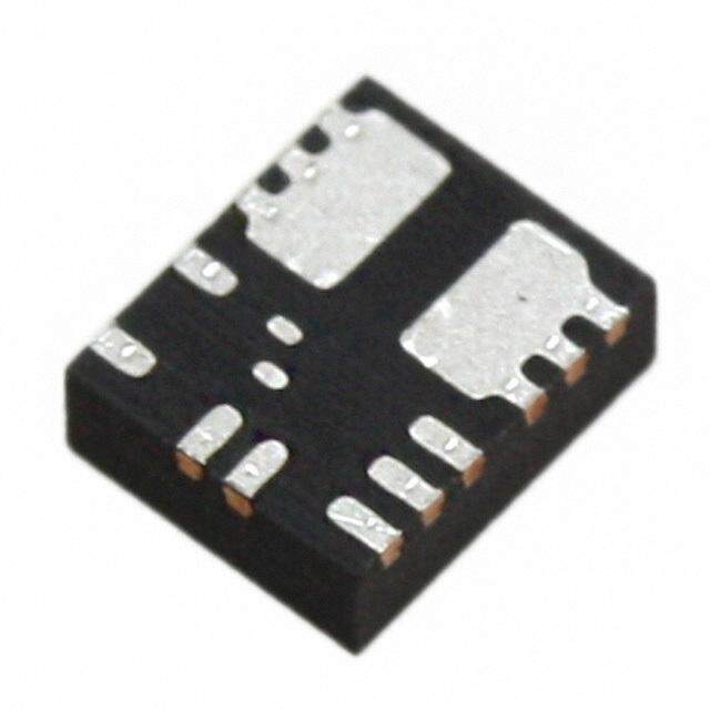
| 产品图片 |
|
| rohs | 符合RoHS无铅 / 符合限制有害物质指令(RoHS)规范要求 |
| 产品系列 | 非隔离式DC/DC转换器,Murata Electronics LXDC2HL1DA-087LXDC2HL |
| 数据手册 | |
| 产品型号 | LXDC2HL1DA-087 |
| 产品 | Non-Isolated / POL |
| 产品种类 | 非隔离式DC/DC转换器 |
| 其它名称 | 490-5792-1 |
| 功率(W)-制造系列 | 1W |
| 功率(W)-最大值 | 1W |
| 包装 | 剪切带 (CT) |
| 商标 | Murata Electronics |
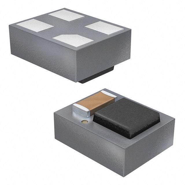
| 大小/尺寸 | 0.10" 长 x 0.08" 宽 x 0.04" 高(2.5mm x 2.0mm x 1.1mm) |
| 安装类型 | 表面贴装 |
| 安装风格 | SMD/SMT |
| 宽度 | 2 mm |
| 封装 | Reel |
| 封装/外壳 | 4-SMD 模块 |
| 封装/箱体尺寸 | 2.5 mm x 2 mm |
| 尺寸 | 2.5 mm x 2 mm x 1.1 mm |
| 工作温度 | -40°C ~ 85°C |
| 工作温度范围 | - 40 C to + 85 C |
| 工厂包装数量 | 3000 |
| 效率 | 82% |
| 标准包装 | 1 |
| 特性 | OCP,UVLO |
| 特色产品 | http://www.digikey.com/product-highlights/cn/zh/murata-electronics-lxdc2hl-micro-dc-dc-converter/1180 |
| 电压-输入(最大值) | 5.5V |
| 电压-输入(最小值) | 2.3V |
| 电压-输出1 | 1.35V |
| 电压-输出2 | - |
| 电压-输出3 | - |
| 电压-隔离 | - |
| 电流-输出(最大值) | 600mA |
| 类型 | 非隔离 PoL 模块 |
| 系列 | LXDC2HL |
| 输入电压—公称值 | 3.6 V |
| 输入电压范围 | 2.3 V to 5.5 V |
| 输出数 | 1 |
| 输出电压—通道1 | 1.35 V |
| 输出电流—通道1 | 600 mA |
| 输出端数量 | 1 |
| 输出类型 | Single |
| 长度 | 2.5 mm |
| 高度 | 1.1 mm |


- 商务部:美国ITC正式对集成电路等产品启动337调查
- 曝三星4nm工艺存在良率问题 高通将骁龙8 Gen1或转产台积电
- 太阳诱电将投资9.5亿元在常州建新厂生产MLCC 预计2023年完工
- 英特尔发布欧洲新工厂建设计划 深化IDM 2.0 战略
- 台积电先进制程称霸业界 有大客户加持明年业绩稳了
- 达到5530亿美元!SIA预计今年全球半导体销售额将创下新高
- 英特尔拟将自动驾驶子公司Mobileye上市 估值或超500亿美元
- 三星加码芯片和SET,合并消费电子和移动部门,撤换高东真等 CEO
- 三星电子宣布重大人事变动 还合并消费电子和移动部门
- 海关总署:前11个月进口集成电路产品价值2.52万亿元 增长14.8%


PDF Datasheet 数据手册内容提取
LXDC2HL series Micro DC-DC converter 1. Features Low EMI noise and small footprint (5mm2) using inductor-embedded ferrite substrate High efficiency using synchronous rectifier technology at 3MHz operation PFM/PWM automatic mode switching function Smooth mode transition between PFM mode and PWM mode with low-ripple-voltage PFM mode 2% DC voltage accuracy over full load current range Wide input voltage range : 2.3~5.5V Maximum Load Current: 600mA (depends on output voltage) Fixed output voltage: 0.8V – 4V (factory setting, 50mV step) Internal soft start, overcurrent protection 2. Description The LXDC2HL series is a low power step-down DC-DC converter suitable for space-limited or noise-sensitive applications. The device utilizes an inductor-embedded ferrite substrate that reduces radiated EMI noise and conduction noise. By adding input/output capacitors, it can be used as an LDO replacement. Its low noise and easy-to-assemble features assure reliable power supply quality. The device works in PFM mode at light load for extended battery life. At heavy load, it changes to PMW mode automatically and maintains high efficiency using synchronous rectifying technology. The device provides good output voltage accuracy even in PFM mode. It maintains 2% DC voltage accuracy over the full current range (0-600mA), and shows very smooth mode transition between PFM mode and PWM mode. 3. Typical Application Circuit LXDC2HL Enable EN Vout VBAT Vin Vout 1.8V/600mA GND 4.7uF 10uF 1 July 2015
LXDC2HL series Micro DC-DC converter 4. Mechanical details 4-1 Outline Top View Device&Trace 1 pin Mark a Bottom View Code 1 2 b X W X2Xあ c 4 3 L c IC Side View Capacitor T Substrate Unit: mm Mark Dimension L 2.5 +/- 0.2 W 2.0 +/- 0.2 T 1.1 MAX a 0.85 +/- 0.1 b 0.60 +/- 0.1 c 0.15 +/- 0.15 4-2. Pin Function Pin Symbol I/O Description 1 Vin Input Vin pin supplies current to the LXDC2HL internal regulator. This is the ON/OFF control pin of the device. Connecting this pin to GND keeps the device in shutdown mode. Pulling this pin to Vin enables the device with soft start. 2 EN Input This pin must not be left floating and must be terminated. If this pin is left open, the device may be off around 100mA output. EN=H: Device ON, EN=L: Device OFF Regulated voltage output pin. 3 Vout Output Apply output load between this pin and GND. 4 GND - Ground pin 2 July 2015
LXDC2HL series Micro DC-DC converter 4-3. Functional Block Diagram EN Vin On-board Cin Clock UVLO Soft Start Switching Controler EA Embedded L Gate Vout Driver Control IC LXDC2HL GND 5. Ordering Information Part number Output Voltage Device Specific Feature MOQ LXDC2HL10A-080 1.0V Standard Type T/R, 3000pcs/R LXDC2HL11A-314 1.1V Standard Type T/R, 3000pcs/R LXDC2HL12A-050 1.2V Standard Type T/R, 3000pcs/R LXDC2HL1CA-322 1.25V Standard Type T/R, 3000pcs/R LXDC2HL13A-082 1.3V Standard Type T/R, 3000pcs/R LXDC2HL1DA-087 1.35V Standard Type T/R, 3000pcs/R LXDC2HL15A-051 1.5V Standard Type T/R, 3000pcs/R LXDC2HL18A-052 1.8V Standard Type T/R, 3000pcs/R LXDC2HL23A-323 2.3V Standard Type T/R, 3000pcs/R LXDC2HL25A-053 2.5V Standard Type T/R, 3000pcs/R LXDC2HL28A-243 2.8V Standard Type T/R, 3000pcs/R LXDC2HL30A-054 3.0V Standard Type T/R, 3000pcs/R LXDC2HL33A-055 3.3V Standard Type T/R, 3000pcs/R # Output voltage can be set 50mV step from 0.8V to 4.0V. Please ask Murata representative. 3 July 2015
LXDC2HL series Micro DC-DC converter 6. Electrical Specification 6-1 Absolute maximum ratings Parameter Symbol rating Unit Input voltage Vin, EN 6.3 V Operating ambient temperature Ta -40 to +85 oC Operating IC temperature T -40 to +125 oC IC Storage temperature T -40 to +85 oC STO 6-2 Electrical characteristics (Ta=25℃) Parameter Symbol Condition Min. Typ. Max. Unit Input voltage V 2.3 3.6 5.5 V in UVLO voltage UVLO 1.0 1.4 1.8 V LXDC2HL10A-080 LXDC2HL11A-314 LXDC2HL12A-050 LXDC2HL1CA-322 Vin=3.6V, LXDC2HL13A-082 EN=0V LXDC2HL1DA-087 Input leak current lin-off LXDC2HL15A-051 0 2 uA LXDC2HL18A-052 LXDC2HL23A-323 LXDC2HL25A-053 LXDC2HL28A-243 Vin=5.0V, LXDC2HL30A-054 EN=0V LXDC2HL33A-055 LXDC2HL10A-080 0.976 1.0 1.024 LXDC2HL11A-314 1.076 1.1 1.124 LXDC2HL12A-050 1.176 1.20 1.224 LXDC2HL1CA-322 1.225 1.25 1.275 LXDC2HL13A-082 1.274 1.30 1.326 Vin-Vout>1V LXDC2HL1DA-087 1.323 1.35 1.377 Output voltage Vout LXDC2HL15A-051 1.47 1.50 1.53 V accuracy LXDC2HL18A-052 1.764 1.80 1.836 LXDC2HL23A-323 2.254 2.30 2.346 LXDC2HL25A-053 2.45 2.50 2.55 LXDC2HL28A-243 2.744 2.80 2.856 Vin-Vout>0.7V LXDC2HL30A-054 2.94 3.00 3.06 Vin-Vout>0.5V LXDC2HL33A-055 3.234 3.30 3.366 4 July 2015
LXDC2HL series Micro DC-DC converter Parameter Symbol Condition Min. Typ. Max. Unit LXDC2HL10A-080 LXDC2HL11A-314 LXDC2HL12A-050 LXDC2HL1CA-322 0 600 LXDC2HL13A-082 LXDC2HL1DA-087 Load current range Iout LXDC2HL15A-051 mA LXDC2HL18A-052 LXDC2HL23A-323 0 500 LXDC2HL25A-053 LXDC2HL28A-243 0 450 LXDC2HL30A-054 0 400 LXDC2HL33A-055 0 300 LXDC2HL10A-080 LXDC2HL11A-314 LXDC2HL12A-050 LXDC2HL1CA-322 Vin=3.6V, LXDC2HL13A-082 Iout=300mA, BW=100MHz LXDC2HL1DA-087 Ripple voltage Vrpl LXDC2HL15A-051 15 mV LXDC2HL18A-052 LXDC2HL23A-323 LXDC2HL25A-053 Vin=5V, LXDC2HL28A-243 Iout=300mA, LXDC2HL30A-054 BW=100MHz LXDC2HL33A-055 5 July 2015
LXDC2HL series Micro DC-DC converter Parameter Symbol Condition Min. Typ. Max. Unit LXDC2HL10A-080 78 LXDC2HL11A-314 79 LXDC2HL12A-050 80 LXDC2HL1CA-322 81 Vin=3.6V, LXDC2HL13A-082 81 Iout=150mA LXDC2HL1DA-087 82 Efficiency EFF LXDC2HL15A-051 83 % LXDC2HL18A-052 85 LXDC2HL23A-323 87 LXDC2HL25A-053 88 Vin=5V, LXDC2HL28A-243 86 Iout=150mA LXDC2HL30A-054 87 LXDC2HL33A-055 88 VENH ON ; Enable 1.4 Vin V EN control voltage VENL OFF ; Disable 0 0.25 V SW Frequency Fosc 2.5 3.0 3.5 MHz LXDC2HL10A-080 LXDC2HL11A-314 LXDC2HL12A-050 LXDC2HL1CA-322 600 900 1200 LXDC2HL13A-082 LXDC2HL1DA-087 LXDC2HL15A-051 mA LXDC2HL18A-052 OCP LXDC2HL23A-323 Over current 500 900 1200 protection LXDC2HL25A-053 LXDC2HL28A-243 500 900 1200 LXDC2HL30A-054 400 700 1200 LXDC2HL33A-055 300 700 1200 If the over current event continues less than Tlatch, auto-recovery. If the over current event continues more than Tlatch, latch-up. Restart by toggling EN voltage or Vin voltage Latch-up mask time Tlatch 20 usec @Vout=0.8×Vnom Start-up time Ton 0.9 msec (*1) External capacitors (Cin: 4.7uF, Cout: 10uF) should be placed near the module for proper operation. (*2) The above characteristics are tested using the test circuit in section 8. 6 July 2015
LXDC2HL series Micro DC-DC converter 6-3 Thermal and Current De-rating Information The following figures show the power dissipation and temperature rise characteristics. These data are measured on Murata’s evaluation board of this device at no air-flow condition. Io -Loss Characteristics (Vin=3.6V, Vo=1.8V) Loss -ΔTCharacteristics (Vin=3.6V, Vo=1.8V) 400 50 45 350 40 W) 300 35 m on ( 250 30 er Dissipati 125000 )oΔT (C 2205 Pow 100 15 10 50 5 0 0 0 100 200 300 400 500 600 0 100 200 300 400 Io (mA) Power Dissipation (mW) The output current of the device may need to be de-rated if it is operated in a high ambient temperature or in a continuous power delivering application. The amount of current de-rating is highly dependent on the environmental thermal conditions, i.e. PCB design, nearby components or effective air flows. Care should especially be taken in applications where the device temperature exceeds 85oC. The IC temperature of the device must be kept lower than the maximum rating of 125 oC. It is generally recommended to take an appropriate de-rating to IC temperature for a reliable operation. A general de-rating for the temperature of semiconductor is 80%. MLCC capacitor’s reliability and the lifetime is also dependant on temperature and applied voltage stress. Higher temperature and/or higher voltage cause shorter lifetime of MLCC, and the degradation can be described by the Arrhenius model. The most critical parameter of the degradation is IR (Insulation Resistance). The below figure shows MLCC’s B1 life based on a failure rate reaching 1%. It should be noted that wear-out mechanisms in MLCC capacitor is not reversible but cumulative over time. 7 July 2015
LXDC2HL series Micro DC-DC converter Capacitor B1 Life vs Capacitor Case temperature 100000 Vin=5V ) Vin=3.6V ours)ours 10000 Vin=3.3V HH d d Vin=2.5V nn 1000 aa ss uu oo 1 Life (TLife(Th 100 or BB1 10 acitor apcit Ca 1 p a C 0.1 20 40 60 80 100 120 CaCpaapcaictoitor r CCaassee Tteemmppreartuarteu r(eo(C℃ )) The following steps should be taken before the design fix of user’s set for reliable operation. 1. The ambient temperature of the device should be kept below 85 oC 2. The IC temperature should be measured on the worst condition of each application. The temperature must be kept below 125 oC. An appropriate de-rating of temperature and/or output current should be taken. 3. The MLCC temperature should be measured on the worst condition of each application. Considering the above figure, it should be checked if the expected B1 life of MLCC is acceptable or not. 8 July 2015
LXDC2HL series Micro DC-DC converter 7. Detailed Description PFM/PWM Mode If the load current decreases, the converter will enter PFM mode automatically. In PFM mode, the device operates in discontinuous current mode with a sporadic switching pulse to keep high efficiency at light load. The device uses constant on-time control in PFM operation, which produces a low ripple voltage and accurate output voltage compared with other PFM architectures. Because of the architecture, DC output voltage can be kept within +/-2% range of the nominal voltage and the output ripple voltage in PFM mode can be reduced by just increasing the output capacitor. The transition between PFM and PWM is also seamless and smooth. The transition current between PFM and PWM is dependent on Vin, Vout and other factors, but the approximate threshold is about 100-200mA. PFM mode at light load PWM mode at heavy load Nominal output voltage UVLO (Under Voltage Lock Out) The input voltage (Vin) must reach or exceed the UVLO voltage (1.4Vtyp) before the device begins the start up sequence even when the EN pin is kept high. The UVLO function protects against unstable operation at low Vin levels . Soft Start The device has an internal soft-start function that limits the inrush current during start-up. The soft-start system progressively increases the switching on-time from a minimum pulse-width to that of normal operation. Because of this function, the output voltage increases gradually from zero to nominal voltage at start-up event. The nominal soft-start time is 0.9msec. If you prefer a faster soft-start time, please contact a Murata representative. Enable The device starts operation when EN is set high and starts up with soft start. For proper operation, the EN pin must be terminated to logic high and must not be left floating. If the pin is left open, the device may operate at light load but will not work at heavy load. Pulling the EN pin to logic low forces the device into shutdown. The device does not have a discharge function when it turns off. If you prefer a discharge function, please contact a Murata representative. 100% Duty Cycle Operation The device can operate in 100% duty cycle mode, in which the high-side switch is constantly turned ON, thereby providing a low input-to-output voltage difference. When Vin and Vout become close and the duty cycle approaches 100%, the switching pulse will skip the nominal switching period and the output voltage ripple may be larger than other conditions. It should be noted that this condition does not mean a failure of the device. Over Current Protection When the output current reaches the OCP threshold, the device narrows the switching duty and decreases the output voltage. If the OCP event is removed within the mask time (20usec typ), the output voltage recovers to the nominal value automatically. If the OCP event continues over the mask time, the device will shutdown. After it is shut down, it can be restarted by toggling the Vin or EN voltage. 9 July 2015
LXDC2HL series Micro DC-DC converter 8. Test Circuit EN Vout Vin LXDC2HL Vin Cout V-EN Cin GND RL Cin : 4.7uF/6.3V (GRM188B30J475K) Cout : 10uF/6.3V (GRM188B30J106M) 10 July 2015
LXDC2HL series Micro DC-DC converter 9. Measurement Data Micro DC-DC Converter evaluation board (P2LX0244) Measurement setup The enable switch has three positions. 1. When it is toggled to “ON” side, the device starts operation. 2. When it is toggled to “OFF” side, the device stops operation and remains in shut down status. 3. When it is set to middle of “ON” and “OFF”, the EN pin floats and an external voltage can be applied to the EN terminal pin on the EVB. If you don’t apply an external voltage to EN pin, the enable switch should not to be set to the middle position. ※The 47uF capacitor is for the evaluation kit only, and has been added to compensate for the long test cables. 11 July 2015
LXDC2HL series Micro DC-DC converter Typical Measurement Data (reference purpose only) (Ta=25℃) Efficiency ・Vin=3.6V, Vout=1.0V ・Vin=3.6V, Vout=1.2V Efficiency Efficiency 80 85 75 80 %] %] F [ 70 F [ 75 EF EF 65 70 60 65 1 10 100 1000 1 10 100 1000 Iout [mA] Iout [mA] ・Vin=3.6V, Vout=1. 3V ・Vin=3.6V, Vout=1.35V Efficiency Efficiency 85 85 80 80 %] %] EFF [75 EFF [ 75 70 70 65 65 1 10 100 1000 1 10 100 1000 Iout [mA] Iout [mA] ・Vin=3.6V, Vout=1.5V ・Vin=3.6V, Vout=1.8V Efficiency Efficiency 85 90 80 85 %] %] F [ 75 F [ 80 EF EF 70 75 65 70 1 10 100 1000 1 10 100 1000 Iout [mA] Iout [mA] 12 July 2015
LXDC2HL series Micro DC-DC converter ・Vin=5.0V, Vout=2.5V ・Vin=5.0V, Vout=3.0V Efficiency Efficiency 95 95 90 90 %] %] F [ 85 F [ 85 F F E E 80 80 75 75 1 10 100 1000 1 10 100 1000 Iout [mA] Iout [mA] ・Vin=5.0V, Vout=3.3V Efficiency 95 90 %] F [ 85 F E 80 75 1 10 100 1000 Iout [mA] 13 July 2015
LXDC2HL series Micro DC-DC converter Typical Measurement Data (reference purpose only) (Ta=25℃) Load Regulation ・Vin=3.6V, Vout=1.0V ・Vin=3.6V, Vout=1.2V Load Regulation Load Regulation 1.024 1.224 1.012 1.212 V] V] t [ t [ u u o o V 1.000 V 1.200 0.988 1.188 0 100 200 300 400 500 600 0 100 200 300 400 500 600 Iout [mA] Iout [mA] ・Vin=3.6V, Vout=1.3V ・Vin=3.6V, Vout=1.35V Load Regulation Load Regulation 1.326 1.377 1.313 1.364 V] V] ut [ 1.300 ut [ 1.350 o o V V 1.287 1.337 1.274 1.323 0 100 200 300 400 500 600 0 100 200 300 400 500 600 Iout [mA] Iout [mA] ・Vin=3.6V, Vout=1.5V ・Vin=3.6V, Vout=1.8V Load Regulation Load Regulation 1.530 1.836 1.515 1.818 ut [V] 1.500 ut [V] 1.800 Vo Vo 1.485 1.782 1.470 1.764 0 100 200 300 400 500 600 0 100 200 300 400 500 600 Iout [mA] Iout [mA] 14 July 2015
LXDC2HL series Micro DC-DC converter ・Vin=5.0V, Vout=2.5V ・Vin=5.0V, Vout=3.0V Load Regulation Load Regulation 2.550 3.060 2.525 3.030 V] V] t [ 2.500 t [ 3.000 u u o o V V 2.475 2.970 2.450 2.940 0 100 200 300 400 500 600 0 100 200 300 400 500 600 Iout [mA] Iout [mA] ・Vin=5.0V, Vout=3.3V Load Regulation 3.366 3.333 V] t [ 3.300 ou V 3.267 3.234 0 100 200 300 400 500 600 Iout [mA] 15 July 2015
LXDC2HL series Micro DC-DC converter Typical Measurement Data (reference purpose only) Output Ripple-Noise ・Vin=3.6V, Vout=1.0V, BW : 150MHz ・Vin=3.6V, Vout=1.2V, BW: 150MHz Output Ripple Noise Output Ripple Noise 50 50 45 45 40 40 35 35 V] 30 V] 30 [m 25 [m 25 pl 20 pl 20 Vr 15 Vr 15 10 10 5 5 0 0 0 100 200 300 400 500 600 0 100 200 300 400 500 600 Iout [mA] Iout [mA] ・Vin=3.6V, Vout=1. 3V, BW: 150MHz ・Vin=3.6V, Vout=1.35V, BW: 150MHz Output Ripple Noise Output Ripple Noise 50 50 45 45 40 40 35 35 V]30 V] 30 m m Vrpl [122505 Vrpl [ 122505 10 10 5 5 0 0 0 100 200 300 400 500 600 0 100 200 300 400 500 600 Iout [mA] Iout [mA] ・Vin=3.6V, Vout=1.5V, BW: 150MHz ・Vin=3.6V, Vout=1.8V, BW: 150MHz Output Ripple Noise Output Ripple Noise 50 50 45 45 40 40 35 35 V] 30 V] 30 m m [ 25 [ 25 pl 20 pl 20 Vr 15 Vr 15 10 10 5 5 0 0 0 100 200 300 400 500 600 0 100 200 300 400 500 600 Iout [mA] Iout [mA] 16 July 2015
LXDC2HL series Micro DC-DC converter ・Vin=5.0V, Vout=2.5V, BW: 150MHz ・Vin=5.0V, Vout=3. 0V, BW: 150MHz Output Ripple Noise Output Ripple Noise 50 50 45 45 40 40 35 35 mV] 30 mV] 30 Vrpl [ 122505 Vrpl [ 122505 10 10 5 5 0 0 0 100 200 300 400 500 600 0 100 200 300 400 500 600 Iout [mA] Iout [mA] ・Vin=5.0V, Vout=3.3V, BW: 150MHz Output Ripple Noise 50 45 40 35 V] 30 m [ 25 Vrpl 1250 10 5 0 0 100 200 300 400 500 600 Iout [mA] 17 July 2015
LXDC2HL series Micro DC-DC converter Typical Measurement Data (reference purpose only) (Ta=25℃) Load Transient Response ・Vin=3.6V, Vout=1.0V 100mV/div 58mV -88mV ΔIo=600mA ・Vin=3.6V, Vout=1.2V 100mV/div 58mV -80mV ΔIo=600mA 18 July 2015
LXDC2HL series Micro DC-DC converter ・Vin=3.6V, Vout=1.35V 66mV 100mV/div -86mV ΔIo=600mA ・Vin=3.6V, Vout=1.5V 66mV 100mV/div -86mV ΔIo=600mA 19 July 2015
LXDC2HL series Micro DC-DC converter ・Vin=3.6V, Vout=1.8V 100mV/div 76mV -108mV ΔIo=600mA ・Vin=3.6V, Vout=2.5V 100mV/div 114mV -140mV ΔIo=500mA 20 July 2015
LXDC2HL series Micro DC-DC converter ・Vin=5.0V, Vout=3.0V 100mV/div 106mV -128mV ΔIo=400mA Vin=5.0V, Vout=3.3V 100mV/div 106mV -112mV ΔIo=300mA 21 July 2015
LXDC2HL series Micro DC-DC converter 10.Reliability Tests Result No. Items Specifications Test Methods QTY (NG) 1 Vibration Appearance : Solder specimens on the testing jig Resistance No severe damages (glass fluorine boards) shown in appended Fig.1 by a Pb free solder. The soldering shall be done either by iron or reflow and be conducted with care so that the soldering is uniform and free of defect such as by heat G 18 shock. (0) Frequency : 10~2000 Hz Acceleration : 196 m/s2 Direction : X,Y,Z 3 axis Period : 2 h on each direction Total 6 h. 2 Deflection Solder specimens on the testing jig (glass epoxy boards) shown in appended Fig.2 by a Pb free solder. The soldering shall be done either by G iron or reflow and be conducted with 18 (0) care so that the soldering is uniform and free of defect such as by heat shock. Deflection : 1.6mm 3 Soldering strength 9.8 N Minimum Solder specimens onto test jig shown (Push Strength) below. Apply pushing force at 0.5mm/s until electrode pads are peeled off or ceramics are broken. Pushing force is applied to longitudinal direction. Pushing Direction 18 G (0) Specimen Jig 4 Solderability of 75% of the Immerse specimens first an ethanol Termination terminations is to be solution of rosin, then in a Pb free soldered evenly and solder solution for 3±0.5 sec. at continuously. 245±5 °C. G 18 Preheat : 150 °C, 60 sec. (0) Solder Paste : Sn-3.0Ag-0.5Cu Flux : Solution of ethanol and rosin (25 % rosin in weight proportion) 5 Resistance to Preheat Temperature : 150-180 °C Soldering Heat Preheat Period : 90+/-30 sec. (Reflow) Appearance No severe damages High Temperature : 220 °C High Temp. Period : 20sec. Satisfy Peak Temperature : 260+5/-0 °C G 18 Electrical specifications listed Specimens are soldered twice with (0) specifications in paragraph 6-2. the above condition, and then kept in room condition for 24 h before measurements. 22 July 2015
LXDC2HL series Micro DC-DC converter Result No. Items Specifications Test Methods QTY (NG) 6 High Temp. Temperature:85±2 ℃ Exposure Period:1000+48/-0 h G 18 Room Condition:2~24h (0) 7 Temperature Condition:100 cycles in the following Cycle table Step Temp(°C) Time(min) Min. 1 Operating 30±3 18 G Temp.+0/-3 (0) Max. 2 Operating 30±3 Temp.+3/-0 Appearance No severe damages 8 Humidity Temperature:85±2 ℃ Electrical Satisfy (Steady State) Humidity:80~90%RH specifications specifications listed G in paragraph 6-2. Period:1000+48/-0 h 18 (0) Room Condition:2~24h 9 Low Temp. Temperature:-40±2 ℃ Exposure Period:1000+48/-0 h G Room Condition:2~24h 18 (0) 10 C:200pF、R:0Ω ESD(Machine G TEST Voltage :+/-100V 5 Model) (0) Number of electric discharges:1 11 C:100pF、R:1500Ω ESD(Human G TEST Voltage :+/-1000V 5 Body Model) (0) Number of electric discharges:1 23 July 2015
LXDC2HL series Micro DC-DC converter Fig.1 Land Pattern Unit:mm Symbol Dimensions a 0.85 b 0.60 c 0.5 d 0.2 ・Reference purpose only. 24 July 2015
LXDC2HL series Micro DC-DC converter Fig.2 Testing board Unit:mm ■: Land pattern is same as figure1 Glass-fluorine board t=1.6mm Copper thickness over 35 m Mounted situation Unit:mm Dチeッvicプe 45 45 Test method Unit:mm 20 50 R230 deflection 25 July 2015
LXDC2HL series Micro DC-DC converter 11. Tape and Reel Packing 1)Dimensions of Tape (Plastic tape) Unit: mm 1.5+0.1 0 1.75±0.1 (0.25) (3.5) 8.0±0.2 (2.8) 2.0±0.05 4.0±0.1 (1.25) (2.3) 4.0±0.1 Feeding direction 2) Dimensions of Reel Unit: mm 2±0.5 Φ60 Φ180 Φ13±0.2 (9.0) 13.0±1.4 26 July 2015
LXDC2HL series Micro DC-DC converter 3)Taping Diagrams [1] Feeding Hole : As specified in (1) [2] Hole for chip : As specified in (1) [3] Cover tape : 50um in thickness [4] Base tape : As specified in (1) [3] [1] [2] [3] [4] Feeding Hole Feeding Direction Chip 27 July 2015
LXDC2HL series Micro DC-DC converter 4)Leader and Tail tape A B Components 部品収納部 C Symbol Items Ratings(mm) A No components at trailer min 160 B No components at leader min 100 C Whole leader min 400 5)The tape for chips are wound clockwise and the feeding holes are to the right side as the tape is pulled toward the user. 6)Packaging unit: 3,000 pcs./ reel 7) Material: Base Tape … Plastic Reel … Plastic Antistatic coating for both base tape and reel 8)Peeling of force 0.01.7~ 1N. 0mNa x. 165 to 180 ° Cカoバveーrテ Tーapプe Bベaーseス Tテaーpeプ 28 July 2015
LXDC2HL series Micro DC-DC converter NOTICE 1. Storage Conditions: To avoid damaging the solderability of the external electrodes, be sure to observe the following points. - Store products where the ambient temperature is 15 to 35 °C and humidity 45 to 75% RH. (Packing materials, In particular, may be deformed at the temperature over 40 °C.). - Store products in non corrosive gas (Cl , NH ,SO , No , etc.). 2 3 2 x - Stored products should be used within 6 months of receipt. Solderability should be verified if this period is exceeded This product is applicable to MSL1 (Based on IPC/JEDEC J-STD-020) 2. Handling Conditions: Be careful in handling or transporting the product. Excessive stress or mechanical shock may damage the product because of the nature of ceramics structure. Do not touch the product, especially the terminals, with bare hands. Doing so may result in poor solderability. 3. Standard PCB Design (Land Pattern and Dimensions): All the ground terminals should be connected to ground patterns. Furthermore, the ground pattern should be provided between IN and OUT terminals. Please refer to the specifications for the standard land dimensions. The recommended land pattern and dimensions are shown for a reference purpose only. Electrical, mechanical and thermal characteristics of the product shall depend on the pattern design and material / thickness of the PCB. Therefore, be sure to check the product performance in the actual set. When using underfill materials, be sure to check the mechanical characteristics in the actual set. 29 July 2015
LXDC2HL series Micro DC-DC converter 4. Soldering Conditions: Soldering is allowed up through 2 times. Carefully perform preheating :△T less than 130 °C. When products are immersed in solvent after mounting, pay special attention to maintain the temperature difference within 100 °C. Soldering must be carried out by the above mentioned conditions to prevent products from damage. Contact Murata before use if concerning other soldering conditions. Reflow soldering standard conditions (example) Reflow soldering standard conditions (Example) Use rosin type flux or weakly active flux with a chlorine content of 0.2 wt % or less. 30 July 2015
LXDC2HL series Micro DC-DC converter 5. Cleaning Conditions: The product is not designed to be cleaned after soldering. 6. Operational Environment Conditions: Products are designed to work for electronic products under normal environmental conditions (ambient temperature, humidity and pressure). Therefore, products have no problems to be used under the similar conditions to the above-mentioned. However, if products are used under the following circumstances, it may damage products and leakage of electricity and abnormal temperature may occur. - In an atmosphere containing corrosive gas ( Cl NH SO NO etc.). 2, 3, x, x - In an atmosphere containing combustible and volatile gases. - In a dusty environment. - Direct sunlight - Water splashing place. - Humid place where water condenses. - In a freezing environment. If there are possibilities for products to be used under the preceding clause, consult with Murata before actual use. If static electricity is added to this product, degradation and destruction may be produced. Please use it after consideration enough so that neither static electricity nor excess voltage is added at the time of an assembly and measurement. If product malfunctions may result in serious damage, including that to human life, sufficient fail-safe measures must be taken, including the following: (1) Installation of protection circuits or other protective device to improve system safety (2) Installation of redundant circuits in the case of single-circuit failure 7. Input Power Capacity: Products shall be used in the input power capacity as specified in this specifications. Inform Murata beforehand, in case that the components are used beyond such input power capacity range . 31 July 2015
LXDC2HL series Micro DC-DC converter 8. Limitation of Applications: The products are designed and produced for application in ordinary electronic equipment (AV equipment, OA equipment, telecommunication, etc). If the products are to be used in devices requiring extremely high reliability following the application listed below, you should consult with the Murata staff in advance. - Aircraft equipment. - Aerospace equipment - Undersea equipment. - Power plant control equipment. - Medical equipment. - Transportation equipment (vehicles, trains, ships, etc.). - Automobile equipment which includes the genuine brand of car manufacture, car factory-installed option and dealer-installed option. - Traffic signal equipment. - Disaster prevention / crime prevention equipment. - Data-procession equipment. - Application which malfunction or operational error may endanger human life and property of assets. - Application which related to occurrence the serious damage - Application of similar complexity and/ or reliability requirements to the applications listed in the above. ! Note: Please make sure that your product has been evaluated and confirmed against your specifications when our product is mounted to your product. Product specifications are subject to change or our products in it may be discontinued without advance notice. This catalog is for reference only and not an official product specification document, therefore, please review and approve our official product specification before ordering this product. 32 July 2015