
 Datasheet下载
- 型号: LTM8032IY#PBF
- 制造商: LINEAR TECHNOLOGY
- 库位|库存: xxxx|xxxx
- 要求:
| 数量阶梯 | 香港交货 | 国内含税 |
| +xxxx | $xxxx | ¥xxxx |
查看当月历史价格
查看今年历史价格
LTM8032IY#PBF产品简介:
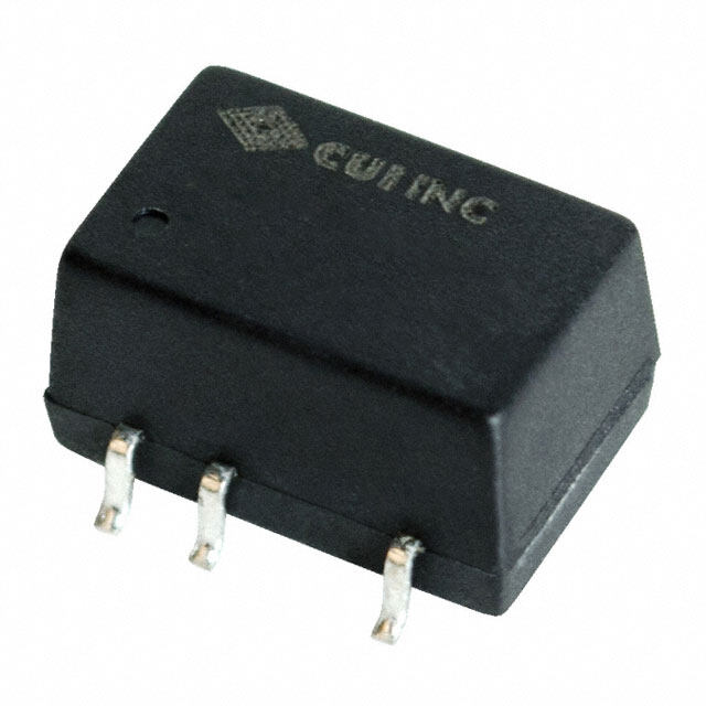
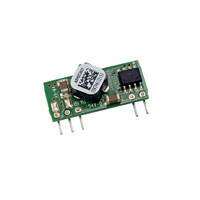
ICGOO电子元器件商城为您提供LTM8032IY#PBF由LINEAR TECHNOLOGY设计生产,在icgoo商城现货销售,并且可以通过原厂、代理商等渠道进行代购。 LTM8032IY#PBF价格参考。LINEAR TECHNOLOGYLTM8032IY#PBF封装/规格:直流转换器, 非隔离 PoL 模块 DC/DC 转换器 1 输出 0.8 ~ 10 V 2A 3.6V - 36V 输入。您可以下载LTM8032IY#PBF参考资料、Datasheet数据手册功能说明书,资料中有LTM8032IY#PBF 详细功能的应用电路图电压和使用方法及教程。
LTM8032IY#PBF 是 Linear Technology(现为 Analog Devices)生产的一款微型模块(µModule®)直流-直流转换器。该器件属于隔离型 DC/DC 转换器,具有宽输入电压范围(3.6V 至 28V)和固定 5V 输出电压的能力,能够提供高达 2.5A 的连续输出电流。以下是 LTM8032 的主要应用场景:

 1. 工业自动化与控制
   - 在工业设备中,LTM8032 可用于为传感器、执行器和通信接口供电。其高效率和隔离特性使其适合在嘈杂的电磁环境中工作。
   - 应用于 PLC(可编程逻辑控制器)、数据采集系统和远程监控设备。

 2. 通信设备
   - 适用于电信基站、网络路由器和交换机等设备中的电源管理。
   - 提供稳定的 5V 输出,支持各种低功耗组件,如微控制器、FPGA 和 ASIC。

 3. 医疗设备
   - 在便携式或台式医疗仪器中,LTM8032 的小型化设计和高效性能使其成为理想选择。
   - 隔离功能有助于满足医疗设备的安全标准,例如防止漏电对患者造成伤害。

 4. 汽车电子
   - 用于车载信息娱乐系统、导航设备和高级驾驶辅助系统(ADAS)。
   - 宽输入电压范围适应汽车电池电压的变化(启动时的电压骤降或过压情况)。

 5. 测试与测量仪器
   - 为精密仪器中的模拟电路和数字电路提供隔离电源,减少噪声干扰。
   - 适用于示波器、信号发生器和其他需要稳定电源的设备。

 6. 航空航天与国防
   - 在严苛环境下运行的设备中,LTM8032 的高可靠性表现突出。
   - 隔离特性有助于保护敏感电路免受高压瞬变的影响。

 7. 消费电子产品
   - 为家用物联网设备、智能家电和便携式设备提供高效电源解决方案。
   - 其紧凑的设计节省了 PCB 空间,非常适合小型化产品。

 特点总结:
- 高集成度:集成了 DC/DC 控制器、功率 MOSFET、变压器和其他支持组件。
- 小型化:采用 BGA 封装,尺寸仅为 9mm x 11.25mm x 4.92mm。
- 高效率:在宽负载范围内保持高效转换。
- 电气隔离:初级和次级之间提供高达 1kV 的隔离电压,增强安全性。

LTM8032IY#PBF 的这些特性使其成为需要高效、可靠且紧凑电源解决方案的理想选择。
| 参数 | 数值 |
| 产品目录 | |
| 描述 | IC DC/DC UMODULE 2A 71BGA |
| 产品分类 | DC DC Converters |
| 品牌 | Linear Technology |
| 数据手册 | http://www.linear.com/docs/27566 |
| 产品图片 |
|
| 产品型号 | LTM8032IY#PBF |
| PCN设计/规格 | |
| rohs | 无铅 / 符合限制有害物质指令(RoHS)规范要求 |
| 产品系列 | LTM®, uModule® |
| 其它名称 | LTM8032IYPBF |
| 功率(W)-制造系列 | 20W |
| 功率(W)-最大值 | 20W |
| 包装 | 托盘 |
| 参考设计库 | http://www.digikey.com/rdl/4294959904/4294959903/569 |
| 大小/尺寸 | 0.59" 长 x 0.35" 宽 x 0.13" 高(15.0mm x 9.0mm x 3.4mm) |
| 安装类型 | 表面贴装 |
| 封装/外壳 | 71-BGA |
| 工作温度 | -40°C ~ 125°C |
| 效率 | - |
| 标准包装 | 170 |
| 特性 | - |
| 特色产品 | http://www.digikey.com/product-highlights/cn/zh/linear-technology-umodule/1305http://www.digikey.com/cn/zh/ph/LT/dcdc.htmlhttp://www.digikey.cn/product-highlights/zh/ltm2884-usb-transceivers/52569 |
| 电压-输入(最大值) | 36V |
| 电压-输入(最小值) | 3.6V |
| 电压-输出1 | 0.8 ~ 10 V |
| 电压-输出2 | - |
| 电压-输出3 | - |
| 电压-隔离 | - |
| 电流-输出(最大值) | 2A |
| 类型 | 非隔离 PoL 模块 |
| 设计资源 | http://www.linear.com/docs/27802 |
| 输出数 | 1 |
| 配用 | /product-detail/zh/DC1386B/DC1386B-ND/2653044 |


- 商务部:美国ITC正式对集成电路等产品启动337调查
- 曝三星4nm工艺存在良率问题 高通将骁龙8 Gen1或转产台积电
- 太阳诱电将投资9.5亿元在常州建新厂生产MLCC 预计2023年完工
- 英特尔发布欧洲新工厂建设计划 深化IDM 2.0 战略
- 台积电先进制程称霸业界 有大客户加持明年业绩稳了
- 达到5530亿美元!SIA预计今年全球半导体销售额将创下新高
- 英特尔拟将自动驾驶子公司Mobileye上市 估值或超500亿美元
- 三星加码芯片和SET,合并消费电子和移动部门,撤换高东真等 CEO
- 三星电子宣布重大人事变动 还合并消费电子和移动部门
- 海关总署:前11个月进口集成电路产品价值2.52万亿元 增长14.8%


PDF Datasheet 数据手册内容提取
LTM8032 EN55022B Compliant 36V, 2A DC/DC µModule Regulator FeaTures DescripTion n Complete Step-Down Switch Mode Power Supply The LTM®8032 is an electromagnetic compatible (EMC) n Wide Input Voltage Range: 3.6V to 36V 36V, 2A DC/DC step-down µModule® regulator designed n 2A Output Current to meet the radiated emissions requirements of EN55022. n 0.8V to 10V Output Voltage Conducted emission requirements can be met by adding n Selectable Switching Frequency: 200kHz to 2.4MHz standard filter components. Included in the package are the n EN55022 Class B Compliant switching controller, power switches, inductor, filters and n Current Mode Control all support components. Operating over an input voltage n Programmable Soft-Start range of 3.6V to 36V, the LTM8032 supports an output n SnPb (BGA) or RoHS Compliant (LGA and BGA) voltage range of 0.8V to 10V, and a switching frequency Finish range of 200kHz to 2.4MHz, each set by a single resistor. n Low Profile, Surface Mount LGA (9mm × 15mm Only the bulk input and output filter capacitors are needed × 2.82mm) and BGA (9mm × 15mm × 3.42mm) to finish the design. The low profile package enables uti- Packages lization of unused space on the bottom of PC boards for high density point of load regulation. applicaTions The LTM8032 is packaged in a thermally enhanced, com- pact and low profile overmolded land grid array (LGA) and n Automotive Battery Regulation ball grid array (BGA) packages suitable for automated n Power for Portable Products assembly by standard surface mount equipment. The n Distributed Supply Regulation LTM8032 is available with SnPb (BGA) or RoHS compli- n Industrial Supplies ant terminal finish. n Wall Transformer Regulation L, LT, LTC, LTM, Linear Technology, the Linear logo, µModule and Burst Mode are registered trademarks of Linear Technology Corporation. All other trademarks are the property of their respective owners. Typical applicaTion Ultralow Noise 5V/2A DC/DC µModule Regulator LTM8032 EMI Performance 7VDC TO 36VVIDNC* VIN VOUT V5VOUT 90 2A 80 FIN 10µF m) 70 RUN/SS AUX µV/ 60 LTM8032 BIAS dB 2.2µF L ( 50 VE EN55022 SHARE PGOOD NS LE 3400 CLILMAISTS B RT SYNC GNDADJ SSIO 20 MI 44.2k 47.5k E 10 8032 TA01a 0 fSW = 700kHz –10 *RUNNING VOLTAGE RANGE. 0 100 200 300 400 500 600 700 800 900 1000 SEE APPLICATIONS FOR START-UP DETAILS FREQUENCY (MHz) 8031 TA01b 8032fg 1 For more information www.linear.com/LTM8032
LTM8032 absoluTe MaxiMuM raTings (Note 1) PGOOD, SYNC...........................................................30V V , FIN, RUN/SS Voltage .........................................40V IN BIAS ..........................................................................25V ADJ, RT, SHARE Voltage .............................................5V V + BIAS .................................................................56V V , AUX .................................................................10V IN OUT Maximum Junction Temperature (Note 2) ............125°C Current from AUX ................................................100mA Solder Temperature ...............................................245°C pin conFiguraTion TOP VIEW TOP VIEW 1 2 3 4 5 6 7 1 2 3 4 5 6 7 VOUT GND VOUT GND A A B B BANK 1 BANK 1 C C D D E E F F BANK 2 BANK 2 G RT G RT H SHARE H SHARE J BIAS AUX ADJ J BIAS AUX ADJ K PGOOD K PGOOD BANK 3 BANK 3 L L VIN FIN RUN/SSSYNC VIN FIN RUN/SSSYNC LGA PACKAGE BGA PACKAGE 71-LEAD (9mm × 15mm × 2.82mm) 71-LEAD (9mm × 15mm × 3.42mm) TJθMJACXto p=θ =1 V 21A55L°.U8C°E, CSθ/J WDA E,= Tθ 2EJ5BR .M=2 °1ICN1/E.W4D°, CPθ/EJWCRb, oJWtEtoSEmIDG =5H 11T-09 =.3 1°C.2/gW , TJθMθJAC VXtoA p=L =1U 21E55S°. 8CD°,E CθT/JEWAR ,= Mθ 2JIN5B .E=6D °1C P1/.EW4R°, CθJ/EJWCDb,E oWCtto E5mI1G =-H9 1,T 15 =.10 -1°1C.22/gW , orDer inForMaTion PART NUMBER PAD OR BALL FINISH PART MARKING* PACKAGE MSL TEMPERATURE RANGE TYPE RATING (Note 2) DEVICE CODE LTM8032EV#PBF Au (RoHS) LTM8032V e4 LGA 3 –40°C to 125°C LTM8032IV#PBF Au (RoHS) LTM8032V e4 LGA 3 –40°C to 125°C LTM8032MPV#PBF Au (RoHS) LTM8032MPV e4 LGA 3 –55°C to 125°C LTM8032EY#PBF SAC305 (RoHS) LTM8032Y e1 BGA 3 –40°C to 125°C LTM8032IY#PBF SAC305 (RoHS) LTM8032Y e1 BGA 3 –40°C to 125°C LTM8032MPY#PBF SAC305 (RoHS) LTM8032Y e1 BGA 3 –55°C to 125°C LTM8032MPY SnPb (63/37) LTM8032Y e0 BGA 3 –55°C to 125°C Consult Marketing for parts specified with wider operating temperature • Recommended LGA and BGA PCB Assembly and Manufacturing ranges. *Device temperature grade is indicated by a label on the shipping Procedures: container. Pad or ball finish code is per IPC/JEDEC J-STD-609. www.linear.com/umodule/pcbassembly • Pb-free and Non-Pb-free Part Markings: • LGA and BGA Package and Tray Drawings: www.linear.com/leadfree www.linear.com/packaging 8032fg 2 For more information www.linear.com/LTM8032
LTM8032 elecTrical characTerisTics The l denotes the specifications which apply over the full internal operating temperature range, otherwise specifications are at T = 25°C. V = 10V, V = 10V, V = 3V, unless otherwise specified. A IN RUN/SS BIAS SYMBOL PARAMETER CONDITIONS MIN TYP MAX UNITS V Input DC Voltage l 3.6 36 V IN V Output DC Voltage 0.2A < I ≤ 2A, R Open 0.8 V OUT OUT ADJ 0.2A < I ≤ 2A, R = 21.6k 10 V OUT ADJ I Continuous Output DC Current V = 24V 2 A OUT IN I V Quiescent Current V = 0.2V 0.6 µA Q(VIN) IN RUN/SS V = 3V, Not Switching l 25 60 µA BIAS V = 0V, Not Switching 88 120 µA BIAS I BIAS Quiescent Current V = 0.2V 0.03 µA Q(BIAS) RUN/SS V = 3V, Not Switching l 60 120 µA BIAS V = 0V, Not Switching 1 5 µA BIAS ∆VOUT Line Regulation 10V ≤ VIN ≤ 36V, IOUT = 1A, VOUT = 3.3V 0.1 % V OUT Load Regulation V = 24V, 0.2A ≤ I ≤ 2A, V = 3.3V 0.3 % IN OUT OUT V Output Ripple (RMS) V = 24V, I = 2A, V = 3.3V 6 mV OUT(AC_RMS) IN OUT OUT f Switching Frequency R = 113k 325 kHz SW T V Voltage at ADJ Pin l 765 790 815 mV ADJ V Minimum BIAS Voltage for Proper Operation 1.9 2.8 V BIAS(MIN) I Current Out of ADJ Pin V = 0V, V = 0V, V = 1V 4 µA ADJ RUN/SS ADJ OUT I RUN/SS Pin Current V = 2.5V 5 10 µA RUN/SS RUN/SS V RUN/SS Input High Voltage 2.5 V IH(RUN/SS) V RUN/SS Input Low Voltage 0.2 V IL(RUN/SS) V ADJ Voltage Threshold for PGOOD to Switch 730 mV PG(TH) I PGOOD Leakage V = 30V 0.1 1 µA PGO PG I PGOOD Sink Current V = 0.4V 200 800 µA PGSINK PG V SYNC Input Low Threshold f = 550kHz 0.5 V SYNCIL SYNC V SYNC Input High Threshold f = 550kHz 0.7 V SYNCIH SYNC I SYNC Pin Bias Current V = 0V, V = 0V 0.1 µA SYNC(BIAS) SYNC BIAS V 550kHz Narrowband Conducted Emission V = 24V, V = 3.3V, I = 2A, f = 550kHz, 89 dBµV IN(RIPPLE) IN OUT OUT SW 1MHz Narrowband Conducted Emission 5µH LISN 69 dBµV 3MHz Narrowband Conducted Emission 51 dBµV Note 1: Stresses beyond those listed under Absolute Maximum Ratings correlation with statistical process controls. LTM8032I is guaranteed may cause permanent damage to the device. Exposure to any Absolute to meet specifications over the full –40°C to 125°C internal operating Maximum Rating condition for extended periods may affect device temperature range. The LTM8032MP is guaranteed to meet specifications reliability and lifetime. over the full –55°C to 125°C internal operating temperature range. Note Note 2: The LTM8032E is guaranteed to meet performance specifications that the maximum internal temperature is determined by specific operating from 0°C to 125°C internal. Specifications over the –40°C to 125°C conditions in conjunction with board layout, the rated package thermal internal temperature range are assured by design, characterization and resistance and other environmental factors. 8032fg 3 For more information www.linear.com/LTM8032
LTM8032 Typical perForMance characTerisTics T = 25°C, unless otherwise noted. A 3.3V Efficiency 5V Efficiency 8V Efficiency OUT OUT OUT 100 100 100 90 90 90 80 80 80 70 70 70 %) %) %) Y ( 60 Y ( 60 Y ( 60 C C C N 50 N 50 N 50 CIE CIE CIE EFFI 40 EFFI 40 EFFI 40 30 30 30 5.5VIN 20 12VIN 20 12VIN 20 12VIN 10 24VIN 10 24VIN 10 24VIN 36VIN 36VIN 36VIN 0 0 0 0.01 0.1 1 10 0.01 0.1 1 10 0.01 0.1 1 10 OUTPUT CURRENT (A) OUTPUT CURRENT (A) OUTPUT CURRENT (A) 8031 G01 8031 G02 8031 G03 Input Current vs Output Current, Input Current vs Output Current, Input Current vs Output Current, 3.3V 5V 8V OUT OUT OUT 1600 1200 1800 5.5VIN 12VIN 12VIN 1400 12VIN 24VIN 1600 24VIN 24VIN 1000 36VIN 36VIN A)1200 36VIN A) A)1400 NT (m1000 NT (m800 NT (m1200 RRE 800 RRE600 RRE1000 CU CU CU 800 PUT 600 PUT 400 PUT 600 N N N I 400 I I 400 200 200 200 0 0 0 0 500 1000 1500 2000 0 500 1000 1500 2000 1 500 1000 1500 2000 OUTPUT CURRENT (mA) OUTPUT CURRENT (mA) OUTPUT CURRENT (mA) 8032 G04 8032 G05 8032 G06 Minimum Required Input Voltage Minimum Required Input Voltage Minimum Required Input Voltage vs Output Voltage, I = 2A vs Load Current, V = 2.5V vs Load Current, V = 3.3V OUT OUT OUT 14 5.0 6.0 12 4.5 5.5 GE (V) 10 GE (V) 4.0 GE (V) 5.0 INPUT VOLTA 68 INPUT VOLTA 33..05 INPUT VOLTA 44..05 4 2.5 3.5 TO RUN TO RUN TO START TO START RUN/SS ENABLED 2 2.0 3.0 0 2 4 6 8 10 0 500 1000 1500 2000 0 500 1000 1500 2000 OUTPUT VOLTAGE (V) LOAD CURRENT (mA) LOAD CURRENT (mA) 8032 G07 8032 G08 8032 G09 8032fg 4 For more information www.linear.com/LTM8032
LTM8032 Typical perForMance characTerisTics T = 25°C, unless otherwise noted. A Minimum Required Input Voltage Minimum Required Input Voltage vs Load Current, V = 5V vs Load Current, V = 8V Bias Current vs Output Current OUT OUT 7.5 11.0 30 3.3VOUT 5VOUT 7.0 10.5 25 8VOUT GE (V) 6.5 GE (V)10.0 T (mA) 20 A A N INPUT VOLT 6.0 INPUT VOLT 99..05 BIAS CURRE 1105 5.5 TO RUN 8.5 TO RUN 5 TO START TO START RUN/SS ENABLED RUN/SS ENABLED 5.0 8.0 0 0 500 1000 1500 2000 0 500 1000 1500 2000 0 500 1000 1500 2000 LOAD CURRENT (mA) LOAD CURRENT (mA) OUTPUT CURRENT (mA) 8032 G10 8032 G11 8032 G12 Output Current vs Input Voltage Input Current vs Input Voltage Temperature Rise vs (Output Shorted) (Output Shorted) Load Current, V = 2.5V (LGA) OUT 3200 1200 35 3000 1000 30 RENT (mA)22680000 ENT (mA)800 E RISE (°C) 2205 UR2400 RR600 UR OUTPUT C22200000 INPUT CU400 TEMPERAT 1150 5VIN 200 5 12VIN 1800 24VIN 36VIN 1600 0 0 0 10 20 30 40 0 10 20 30 40 0 500 1000 1500 2000 2500 INPUT VOLTAGE (V) INPUT VOLTAGE (V) LOAD CURRENT (mA) 8032 G13 8032 G14 8032 G15 Temperature Rise vs Temperature Rise vs Temperature Rise vs Load Current, V = 3.3V (LGA) Load Current, V = 5V (LGA) Load Current, V = 8V (LGA) OUT OUT OUT 40 40 50 45 35 35 40 RISE (°C) 3205 RISE (°C) 3205 RISE (°C) 3305 URE 20 URE 20 URE 25 PERAT 15 PERAT 15 PERAT 20 M M M 15 TE 10 51V2VININ TE 10 12VIN TE 10 12VIN 5 24VIN 5 24VIN 5 24VIN 36VIN 36VIN 36VIN 0 0 0 0 500 1000 1500 2000 2500 0 500 1000 1500 2000 2500 0 500 1000 1500 2000 2500 LOAD CURRENT (mA) LOAD CURRENT (mA) LOAD CURRENT (mA) 8032 G16 8032 G17 8032 G18 8032fg 5 For more information www.linear.com/LTM8032
LTM8032 Typical perForMance characTerisTics T = 25°C, unless otherwise noted. A Temperature Rise vs Load Current, V = 10V (LGA) Radiated Emissions Radiated Emissions OUT m) m) TURE RISE (°C) 345234000555 EMISSIONS LEVEL (dBµV/–9753110000000 1002003004005006007008009001000 EMISSIONS LEVEL (dBµV/–9753110000000 1002003004005006007008009001000 ERA 20 FREQUENCY (MHz) 8031 G20 FREQUENCY (MHz) 8031 G21 MP 15 VIN = 36V VIN = 13V TE VOUT = 10V AT 2A VOUT = 10V AT 2A 10 5 24VIN 36VIN 0 0 500 1000 1500 2000 2500 LOAD CURRENT (mA) 8032 G19 Temperature Rise vs Temperature Rise vs Load Current, VOUT = 2.5V (BGA) Load Current, VOUT = 3.3V (BGA) 35 35 30 30 RE RISE (°C) 2205 RE RISE (°C) 2250 U U RAT 15 RAT 15 TEMPE 10 5VIN TEMPE 10 5 1224VVIINN 5 1224VVIINN 36VIN 36VIN 0 0 0 500 1000 1500 2000 2500 0 500 1000 1500 2000 2500 LOAD CURRENT (mA) LOAD CURRENT (mA) 8032 G22 8032 G23 Temperature Rise vs Temperature Rise vs Load Current, V = 5V (BGA) Load Current, V = 10V (BGA) OUT OUT 40 60 35 50 C) 30 C) E (° E (° 40 S 25 S RI RI E E R 20 R 30 U U T T A A PER 15 PER 20 M M TE 10 TE 12VIN 10 5 24VIN 24VIN 36VIN 36VIN 0 0 0 500 1000 1500 2000 2500 0 500 1000 1500 2000 2500 LOAD CURRENT (mA) LOAD CURRENT (mA) 8032 G24 8032 G25 8032fg 6 For more information www.linear.com/LTM8032
LTM8032 pin FuncTions V (Bank 3): The V pin supplies current to the LTM8032’s RUN/SS (Pin L5): Pull RUN/SS pin to less than 0.2V to IN IN internal regulator and to the internal power switch. This shut down the LTM8032. Tie to 2.5V or more for normal pin must be locally bypassed with an external, low ESR operation. If the shutdown feature is not used, tie this pin capacitor of at least 2.2µF. to the V pin. RUN/SS also provides a soft-start function; IN see the Applications Information section. FIN (K3, L3): Filtered Input. This is the node after the input EMI filter. Use this only if there is a need to modify the RT (Pin G7): The RT pin is used to program the switching behavior of the integrated EMI filter or if V rises or falls frequency of the LTM8032 by connecting a resistor from IN rapidly; otherwise, leave these pins unconnected. See the this pin to ground. The Applications Information section of Applications Information section for more details. the data sheet includes a table to determine the resistance value based on the desired switching frequency. Minimize GND (Bank 2): Tie these GND pins to a local ground plane capacitance at this pin. below the LTM8032 and the circuit components. In most applications, the bulk of the heat flow out of the LTM8032 SHARE (Pin H7): Tie this to the SHARE pin of another is through these pads, so the printed circuit design has a LTM8032 when paralleling the outputs. Otherwise, do not large impact on the thermal performance of the part. See connect (leave floating). the PCB Layout and Thermal Considerations sections for SYNC (Pin L6): This is the external clock synchronization more details. Return the feedback divider (R ) to this net. ADJ input. Ground this pin for low ripple Burst Mode® operation V (Bank 1): Power Output Pins. Apply the output filter at low output loads. Tie to a stable voltage source greater OUT capacitor and the output load between these pins and than 0.7V to disable Burst Mode operation. Do not leave GND pins. this pin floating. Tie to a clock source for synchronization. Clock edges should have rise and fall times faster than 1µs. AUX (Pin H5): Low Current Voltage Source for BIAS. The See synchronization section in Applications Information. AUX pin is internally connected to V and is placed OUT adjacent to the BIAS pin to ease printed circuit board PGOOD (Pin K7): The PGOOD pin is the open-collector routing. Although this pin is internally connected to V , output of an internal comparator. PGOOD remains low until OUT do not connect this pin to the load. If this pin is not tied the ADJ pin is within 10% of the final regulation voltage. to BIAS, leave it floating. The PGOOD output is valid when V is above 3.6V and IN RUN/SS is high. If this function is not used, leave this BIAS (Pin H4): The BIAS pin connects to the internal power pin floating. bus. Connect to a power source greater than 2.8V. If the output is greater than 2.8V, connect this pin to AUX. If ADJ (Pin J7): The LTM8032 regulates its ADJ pin to 0.79V. the output voltage is less, connect this to a voltage source Connect the adjust resistor from this pin to ground. The between 2.8V and 25V. Also, make sure that BIAS + V value of R is given by the equation: IN ADJ is less than 56V. 196.71 R = ADJ V –0.79 OUT where R is in kΩ. ADJ 8032fg 7 For more information www.linear.com/LTM8032
LTM8032 block DiagraM FIN EMI FILTER VIN 4.7µH VOUT AUX 249k 10µF GND GND BIAS SHARE CURRENT MODE CONTROLLER RUN/SS SYNC RT PGOOD ADJ 8032 BD 8032fg 8 For more information www.linear.com/LTM8032
LTM8032 operaTion The LTM8032 is a standalone nonisolated step-down An internal regulator provides power to the control circuitry. switching DC/DC power supply. It can deliver up to 2A of The bias regulator can draw power from the V pin, but if IN DC output current with only bulk external input and output the BIAS pin is connected to an external voltage higher than capacitors. This module provides a precisely regulated 2.8V, bias power will be drawn from the external source output voltage programmable via one external resistor (typically the regulated output voltage). This improves from 0.8VDC to 10VDC. The input voltage range is 3.6V efficiency. The RUN/SS pin is used to place the LTM8032 to 36V. Given that the LTM8032 is a step-down converter, in shutdown, disconnecting the output and reducing the make sure that the input voltage is high enough to support input current to less than 1µA. the desired output voltage and load current. A simplified To further optimize efficiency, the LTM8032 automatically Block Diagram is given on the previous page. switches to Burst Mode operation in light load situations. The LTM8032 is designed with an input EMI filter and other Between bursts, all circuitry associated with controlling features to make its radiated emissions compliant with the output switch is shut down reducing the input supply several EMC specifications including EN55022 class B. current to 50µA in a typical application. The oscillator Compliance with conducted emissions requirements may reduces the LTM8032’s operating frequency when the be obtained by adding a standard input filter. voltage at the ADJ pin is low. This frequency foldback helps to control the output current during start-up and overload. The LTM8032 contains a current mode controller, power switching element, power inductor, power Schottky diode The LTM8032 contains a power good comparator which and a modest amount of input and output capacitance. trips when the ADJ pin is at 90% of its regulated value. The LTM8032 is a fixed frequency PWM regulator. The The PGOOD output is an open-collector transistor that is switching frequency is set by simply connecting the ap- off when the output is in regulation, allowing an external propriate resistor value from the RT pin to GND. resistor to pull the PGOOD pin high. Power good is valid when the LTM8032 is enabled and V is above 3.6V. IN applicaTions inForMaTion For most applications, the design process is straight Capacitor Selection Considerations forward, summarized as follows: The C and C capacitor values in Table 1 are the IN OUT 1. Look at Table 1 and find the row that has the desired minimum recommended values for the associated oper- input range and output voltage. ating conditions. Applying capacitor values below those indicated in Table 1 is not recommended, and may result 2. Apply the recommended C , C , R and R IN OUT ADJ T in undesirable operation. Using larger values is generally values. acceptable, and can yield improved dynamic response, if 3. Connect BIAS as indicated. it is necessary. Again, it is incumbent upon the user to verify proper operation over the intended system’s line, As the integrated input EMI filter may ring in response to load and environmental conditions. an application of a step input voltage, a bulk capacitance, series resistance or some clamping mechanism may be Ceramic capacitors are small, robust and have very low required. See the Hot-Plugging Safely section for details. ESR. However, not all ceramic capacitors are suitable. X5R and X7R types are stable over temperature and ap- While these component combinations have been tested plied voltage and give dependable service. Other types, for proper operation, it is incumbent upon the user to including Y5V and Z5U have very large temperature and verify proper operation over the intended system’s line, voltage coefficients of capacitance. In an application load and environmental conditions. 8032fg 9 For more information www.linear.com/LTM8032
LTM8032 applicaTions inForMaTion Table 1. Recommended Component Values and Configuration V V C C R BIAS f R f R IN OUT IN OUT ADJ OPTIMAL T(OPTIMAL) MAX T(MIN) 3.6V to 36V 0.82V 2.2µF 200µF 1206 5.62M ≥2.8V, <25V 250k 150k 250k 150k 3.6V to 36V 1.00V 2.2µF 200µF 1206 953k ≥2.8V, <25V 300k 124k 300k 124k 3.6V to 36V 1.20V 2.2µF 147µF 1206 487k ≥2.8V, <25V 350k 105k 350k 105k 3.6V to 36V 1.50V 2.2µF 147µF 1206 280k ≥2.8V, <25V 400k 88.7k 400k 88.7k 3.6V to 36V 1.80V 2.2µF 100µF 1206 196k ≥2.8V, <25V 450k 78.7k 450k 78.7k 3.6V to 36V 2.00V 2.2µF 68µF 1206 165k ≥2.8V, <25V 450k 78.7k 450k 78.7k 4.0V to 36V 2.20V 2.2µF 68µF 1206 140k ≥2.8V, <25V 500k 69.8k 500k 69.8k 4.3V to 36V 2.50V 2.2µF 47µF 1206 115k ≥2.8V, <25V 550k 61.9k 600k 54.9k 5.5V to 36V 3.30V 2.2µF 22µF 1206 78.7k AUX 600k 54.9k 700k 44.2k 7V to 36V 5.00V 2.2µF 10µF 1206 47.5k AUX 700k 44.2k 1M 29.4k 10.5V to 36V 8.00V 2.2µF 10µF 1206 27.4k AUX 800k 39.2k 1.5M 16.2k 3.6V to 15V 0.82V 2.2µF 200µF 1206 5.62M V 250k 150k 600k 54.9k IN 3.6V to 15V 1.00V 2.2µF 200µF 1206 953k V 300k 124k 700k 44.2k IN 3.6V to 15V 1.20V 2.2µF 147µF 1206 487k V 350k 105k 800k 39.2k IN 3.6V to 15V 1.50V 2.2µF 147µF 1206 280k V 400k 88.7k 900k 34.0k IN 3.6V to 15V 1.80V 2.2µF 100µF 1206 196k V 450k 78.7k 1M 29.4k IN 3.6V to 15V 2.00V 2.2µF 68µF 1206 165k V 450k 78.7k 1.1M 26.1k IN 4.0V to 15V 2.20V 2.2µF 68µF 1206 140k V 500k 69.8k 1.25M 22.1k IN 4.3V to 15V 2.50V 2.2µF 47µF 1206 115k V 550k 61.9k 1.3M 21.0k IN 5.5V to 15V 3.30V 2.2µF 22µF 1206 78.7k AUX 600k 54.9k 1.7M 14.0k 7V to 15V 5.00V 2.2µF 10µF 1206 47.5k AUX 700k 44.2k 2M 10.0k 9V to 24V 0.82V 2.2µF 200µF 1206 5.62M ≥2.8V, <25V 250k 150k 400k 88.7k 9V to 24V 1.00V 2.2µF 200µF 1206 953k ≥2.8V, <25V 300k 124k 450k 79.0k 9V to 24V 1.20V 2.2µF 147µF 1206 487k ≥2.8V, <25V 350k 105k 500k 69.8k 9V to 24V 1.50V 2.2µF 147µF 1206 280k ≥2.8V, <25V 400k 88.7k 550k 61.9k 9V to 24V 1.80V 2.2µF 100µF 1206 196k ≥2.8V, <25V 450k 78.7k 650k 49.9k 9V to 24V 2.00V 2.2µF 68µF 1206 165k ≥2.8V, <25V 450k 78.7k 700k 44.2k 9V to 24V 2.20V 2.2µF 47µF 1206 140k ≥2.8V, <25V 500k 69.8k 750k 42.2k 9V to 24V 2.50V 2.2µF 22µF 1206 115k ≥2.8V, <25V 550k 61.9k 800k 39.2k 9V to 24V 3.30V 2.2µF 22µF 1206 78.7k AUX 600k 54.9k 1M 29.4k 9V to 24V 5.00V 2.2µF 10µF 1206 47.5k AUX 700k 44.2k 1.5M 16.2k 10.5V to 24V 8.00V 2.2µF 10µF 1206 27.4k AUX 800k 39.2k 1.5M 16.2k 13V to 24V 10.00V 2.2µF 10µF 1206 21.5k AUX 900k 34.0k 1.3M 21.0k 18V to 36V 0.82V 2.2µF 200µF 1206 5.62M ≥2.8V, <25V 250k 150k 250k 150k 18V to 36V 1.00V 2.2µF 200µF 1206 953k ≥2.8V, <25V 300k 124k 300k 124k 18V to 36V 1.20V 2.2µF 147µF 1206 487k ≥2.8V, <25V 350k 105k 350k 105k 18V to 36V 1.50V 2.2µF 147µF 1206 280k ≥2.8V, <25V 400k 88.7k 400k 88.7k 18V to 36V 1.80V 2.2µF 100µF 1206 196k ≥2.8V, <25V 450k 78.7k 450k 78.7k 18V to 36V 2.00V 2.2µF 68µF 1206 165k ≥2.8V, <25V 450k 78.7k 450k 78.7k 18V to 36V 2.20V 2.2µF 47µF 1206 140k ≥2.8V, <25V 500k 69.8k 500k 69.8k 18V to 36V 2.50V 2.2µF 22µF 1206 115k ≥2.8V, <25V 550k 61.9k 600k 54.9k 18V to 36V 3.30V 2.2µF 22µF 1206 78.7k AUX 600k 54.9k 700k 44.2k 18V to 36V 5.00V 2.2µF 10µF 1206 47.5k AUX 700k 44.2k 1M 29.4k 18V to 36V 8.00V 2.2µF 10µF 1206 27.4k AUX 800k 39.2k 1.5M 16.2k 18V to 36V 10.00V 2.2µF 10µF 1206 21.5k AUX 900k 34.0k 1.3M 21.0k Note: An input bulk capacitor is required. 200µF is 2 × 100µF, 147 is 100µF||47µF 8032fg 10 For more information www.linear.com/LTM8032
LTM8032 applicaTions inForMaTion circuit they may have only a small fraction of their nominal Table 2. Switching Frequency vs R Value T capacitance resulting in much higher output voltage ripple SWITCHING FREQUENCY (MHz) R VALUE (kΩ) T than expected. Ceramic capacitors are also piezoelectric. In 0.2 187 Burst Mode operation, the LTM8032’s switching frequency 0.3 124 depends on the load current, and can excite a ceramic 0.4 88.7 capacitor at audio frequencies, generating audible noise. 0.5 69.8 Since the LTM8032 operates at a lower current limit during 0.6 54.9 Burst Mode operation, the noise is typically very quiet to 0.7 44.2 a casual ear. If this audible noise is unacceptable, use a 0.8 39.2 high performance electrolytic capacitor at the output. The 0.9 34 input capacitor can be a parallel combination of a 2.2µF 1.0 29.4 ceramic capacitor and a low cost electrolytic capacitor. 1.2 23.7 A final precaution regarding ceramic capacitors concerns 1.4 19.1 the maximum input voltage rating of the LTM8032. A 1.5 16.2 ceramic input capacitor combined with trace or cable 1.8 13.3 inductance forms a high Q (under damped) tank circuit. 2 11.5 If the LTM8032 circuit is plugged into a live supply, the 2.2 9.76 input voltage can ring to twice its nominal value, possi- 2.4 8.66 bly exceeding the device’s rating. This situation is easily avoided; see the Hot-Plugging Safely section. result in undesirable operation under certain operating or fault conditions. A frequency that is too high can reduce Electromagnetic Compliance efficiency, generate excessive heat or even damage the The LTM8032 is compliant with the radiated emissions LTM8032 if the output is overloaded or short-circuited. requirements of EN55022 class B. Graphs of the LTM8032’s A frequency that is too low can result in a final design EMC performance are given in the Typical Performance that has too much output ripple or too large of an output Characteristics section. Further data, operating conditions cap. The maximum frequency (and attendant R value) at T and test setup are detailed in an EMI Test report available which the LTM8032 should be allowed to switch is given from the Linear Technology website. in Table 1 in the f column, while the recommended MAX frequency (and R value) for optimal efficiency over the T Frequency Selection given input condition is given in the f column. OPTIMAL The LTM8032 uses a constant frequency PWM architecture There are additional conditions that must be satisfied if that can be programmed to switch from 200kHz to 2.4MHz the synchronization function is used. Please refer to the by using a resistor tied from the RT pin to ground. Table 2 Synchronization section for details. provides a list of R resistor values and their resultant T frequencies. BIAS Pin Considerations The BIAS pin is used to provide drive power for the internal Operating Frequency Trade-Offs power switching stage and operate internal circuitry. For It is recommended that the user apply the optimal R proper operation, it must be powered by at least 2.8V. If T value given in Table 1 for the input and output operating the output voltage is programmed to be 2.8V or higher, condition. System level or other considerations, however, simply tie BIAS to AUX. If V is less than 2.8V, BIAS OUT may necessitate another operating frequency. While the can be tied to V or some other voltage source. In all IN LTM8032 is flexible enough to accommodate a wide range cases, ensure that the maximum voltage at the BIAS pin of operating frequencies, a haphazardly chosen one may is both less than 25V and the sum of V and BIAS is less IN 8032fg 11 For more information www.linear.com/LTM8032
LTM8032 applicaTions inForMaTion than 56V. If BIAS power is applied from a remote or noisy To disable Burst Mode operation, tie SYNC to a stable voltage source, it may be necessary to apply a decoupling voltage above 0.7V or synchronize to an external clock. capacitor locally to the LTM8032. Do not leave the SYNC pin floating. Load Sharing Minimum Input Voltage Two or more LTM8032s may be paralleled to produce higher The LTM8032 is a step-down converter, so a minimum currents. This may, however, alter the EMI performance amount of headroom is required to keep the output in of the LTM8032s. To do this, tie the V , ADJ, V and regulation. In addition, the input voltage required to turn IN OUT SHARE pins of all the paralleled LTM8032s together. To on is higher than that required to run, and depends upon ensure that paralleled modules start up together, the RUN/ whether the RUN/SS is used. As shown in Figure 1, it SS pins may be tied together, as well. Synchronize the takes only about 3.6V for the LTM8032 to run a 3.3V IN LTM8032s to an external clock to eliminate beat frequen- output at light load. If RUN/SS is tied directly to V , a IN cies, if required. If the RUN/SS pins are not tied together, 5.5V input voltage is required to start. If V is allowed to IN make sure that the same valued soft-start capacitors settle in the operating region first then the RUN/SS pin is are used for each module. An example of two LTM8032 enabled, the minimum input voltage to start at light load modules configured for load sharing is given in the Typical is lower, about 4.7V. A similar curve for 5V operation OUT Applications section. is also provided in Figure 1. For current sharing applications using multiple LTM8032s, 6.0 the ADJ pins for all regulators may be combined using VOUT = 3.3V one resistor to ground as determined by: 5.5 196.71 E (V) 5.0 G A R = N OLT 4.5 ADJ V V –0.79 T OUT U NP 4.0 I where N is the number of paralleled modules and R ADJ 3.5 TO RUN is in kΩ. TO START RUN/SS ENABLED 3.0 0 500 1000 1500 2000 Burst Mode Operation LOAD CURRENT (mA) To enhance efficiency at light loads, the LTM8032 auto- 8032 F01a matically switches to Burst Mode operation which keeps 7.5 VOUT = 5V the output capacitor charged to the proper voltage while minimizing the input quiescent current. During Burst Mode 7.0 operation, the LTM8032 delivers single cycle bursts of V) current to the output capacitor followed by sleep periods AGE ( 6.5 LT where the output power is delivered to the load by the output VO capacitor. In addition, VIN and BIAS quiescent currents are NPUT 6.0 I reduced to typically 25µA and 60µA respectively during 5.5 TO RUN the sleep time. As the load current decreases towards a TO START no-load condition, the percentage of time that the LTM8032 RUN/SS ENABLED 5.0 operates in sleep mode increases and the average input 0 500 1000 1500 2000 LOAD CURRENT (mA) current is greatly reduced, resulting in higher efficiency. 8032 F01b Burst Mode operation is enabled by tying SYNC to GND. Figure 1. The LTM8032 Needs More Voltage to Start Than Run 8032fg 12 For more information www.linear.com/LTM8032
LTM8032 applicaTions inForMaTion Soft-Start Shorted Input Protection The RUN/SS pin can be used to soft-start the LTM8032, Care needs to be taken in systems where the output will reducing the maximum input current during start-up. The be held high when the input to the LTM8032 is absent. RUN/SS pin is driven through an external RC network to This may occur in battery charging applications or in create a voltage ramp at this pin. Figure 2 shows the start- battery back-up systems where a battery or some other up and shutdown waveforms with the soft-start circuit. By supply is diode ORed with the LTM8032’s output. If the choosing an appropriate RC time constant, the peak start-up V pin is allowed to float and the RUN/SS pin is held high IN current can be reduced to the current that is required to (either by a logic signal or because it is tied to V ), then IN regulate the output, with no overshoot. Choose the value the LTM8032’s internal circuitry will pull its quiescent of the resistor so that it can supply at least 20µA when current through its internal power switch. This is fine if the RUN/SS pin reaches 2.5V. your system can tolerate a few milliamps in this state. If you ground the RUN/SS pin, the internal switch current will drop to essentially zero. However, if the V pin is IN grounded while the output is held high, then parasitic diodes inside the LTM8032 can pull large currents from IL RUN 1A/DIV the output through the V pin, potentially damaging the IN 15k device. Figure 3 shows a circuit that will run only when RUN/SS VRUN/SS the input voltage is present and that protects against a 2V/DIV 0.22µF GND shorted or reversed input. VOUT 2V/DIV VIN VIN VOUT VOUT 2ms/DIV 8023 F02 RUN/SS AUX LTM8032 Figure 2. To Soft-Start the LTM8032, Add a Resistor BIAS and Capacitor to the RUN/SS Pin ADJ RT SYNC GND Synchronization The internal oscillator of the LTM8032 can be synchro- 8032 F03 nized by applying an external 250kHz to 2MHz clock to the SYNC pin. Do not leave this pin floating. The resistor Figure 3. The Input Diode Prevents a Shorted Input from tied from the RT pin to ground should be chosen such Discharging a Back-Up Battery Tied to the Output. It Also that the LTM8032 oscillates 20% lower than the intended Protects the Circuit from a Reversed Input. The LTM8032 Runs Only When the Input is Present synchronization frequency (see the Frequency Selection section). The LTM8032 will not enter Burst Mode operation while synchronized to an external clock, but will instead skip pulses to maintain regulation. 8032fg 13 For more information www.linear.com/LTM8032
LTM8032 applicaTions inForMaTion PCB Layout as possible to the FIN terminals, such that its ground connection is as close as possible to that of the C Most of the headaches associated with PCB layout have IN capacitor. been alleviated or even eliminated by the high level of integration of the LTM8032. The LTM8032 is neverthe- 3. Place the C capacitor as close as possible to the OUT less a switching power supply and care must be taken to V and GND connection of the LTM8032. OUT minimize EMI and ensure proper operation. Even with the 4. Place the C and C capacitors such that their IN OUT high level of integration, you may fail to achieve specified ground currents flow directly adjacent or underneath operation with a haphazard or poor layout. See Figure 4 the LTM8032. for a suggested layout. 5. Connect all of the GND connections to as large a copper Ensure that the grounding and heat sinking are acceptable. pour or plane area as possible on the top layer. Avoid A few rules to keep in mind are: breaking the ground connection between the external 1. Place the R and R resistors as close as possible to components and the LTM8032. ADJ T their respective pins. 6. Use vias to connect the GND copper area to the board’s 2. Place the C capacitor as close as possible to the V internal ground plane. Liberally distribute these GND vias IN IN and GND connection of the LTM8032. If a capacitor to provide both a good ground connection and thermal is connected to the FIN terminals, place it as close path to the internal planes of the printed circuit board. GND RT ADJ OD R O G P COUT SYNC AUX RUN/SS BIAS FIN VIN OPTIONAL FIN CAPACITOR VOUT CIN GND 8032 F04 Figure 4. Layout Showing Suggested External Components, GND Plane and Thermal Vias (LGA Package) 8032fg 14 For more information www.linear.com/LTM8032
LTM8032 applicaTions inForMaTion Hot-Plugging Safely with a 2.2µF ceramic capacitor at the input. The input voltage rings as high as 35V and the input current peaks The small size, robustness and low impedance of ceramic at 20A. One method of damping the tank circuit is to add capacitors make them an attractive option for the input another capacitor with a series resistor to the circuit. An bypass capacitor of LTM8032. However, these capacitors alternative solution is shown in Figure 5b. A 0.7Ω resistor can cause problems if the LTM8032 is plugged into a live is added in series with the input to eliminate the voltage or fast rising or falling supply (see Linear Technology overshoot (it also reduces the peak input current). A 0.1µF Application Note 88 for a complete discussion). The low capacitor improves high frequency filtering. For high input loss ceramic capacitor combined with stray inductance in voltages its impact on efficiency is minor, reducing ef- series with the power source forms an under-damped tank ficiency less than one-half percent for a 5V output at full circuit, and the voltage at the V pin of the LTM8032 can IN load operating from 24V. By far the most popular method ring to twice the nominal input voltage, possibly exceeding of controlling overshoot is shown in Figure 5c, where an the LTM8032’s rating and damaging the part. A similar aluminum electrolytic capacitor has been connected to FIN. phenomenon can occur inside the LTM8032 module, at the This capacitor’s high equivalent series resistance damps output of the integrated EMI filter, with the same potential the circuit and eliminates the voltage overshoot. The extra of damaging the part. capacitor improves low frequency ripple filtering and can If the input supply is poorly controlled or the user will be slightly improve the efficiency of the circuit, though it is plugging the LTM8032 into an energized supply, the input likely to be the largest component in the circuit. Figure 5c network should be designed to prevent this overshoot. Fig- shows the capacitor added to the V terminals, but placing IN ure 5 shows the waveforms that result when an LTM8032 the electrolytic capacitor at the FIN terminals can improve circuit is connected to a 24V supply through six feet of the LTM8032’s EMI filtering as well as guard against 24-gauge twisted pair. The first plot (5a) is the response overshoots caused by the Q of the integrated filter. 8032fg 15 For more information www.linear.com/LTM8032
LTM8032 applicaTions inForMaTion CLOSING SWITCH DANGER SIMULATES HOT PLUG VIN IIN LTM8032 20V/DIV VIN RINGING VIN MAY EXCEED + ABSOLUTE MAXIMUM RATING 4.7µF LOW STRAY IIN 10A/DIV IMPEDANCE INDUCTANCE ENERGIZED DUE TO 6 FEET 24V SUPPLY (2 METERS) OF 20µs/DIV TWISTED PAIR (5a) 0.7Ω LTM8032 VIN VIN 20V/DIV + 0.1µF 4.7µF IIN 10A/DIV 20µs/DIV (5b) FIN LTM8032 VIN VIN 20V/DIV + + 22µF 35V 4.7µF AI.EI. IIN 10A/DIV 20µs/DIV 8032 F05 (5c) Figure 5. A Well Chosen Input Network Prevents Input Voltage Overshoot and Ensures Reliable Operation When the LTM8032 is Hot-Plugged to a Live Supply 8032fg 16 For more information www.linear.com/LTM8032
LTM8032 applicaTions inForMaTion Thermal Considerations While the meaning of each of these coefficients may seem to be intuitive, JEDEC has defined each to avoid confu- The LTM8032 output current may need to be derated if sion and inconsistency. These definitions are given in it is required to operate in a high ambient temperature or JESD 51-12, and are quoted or paraphrased in the following: deliver a large amount of continuous power. The amount of current derating is dependent upon the input voltage, • θ is the natural convection junction-to-ambient air JA output power and ambient temperature. The temperature thermal resistance measured in a one cubic foot sealed rise curves given in the Typical Performance Character- enclosure. This environment is sometimes referred to as istics section can be used as a guide. These curves were “still air” although natural convection causes the air to generated by an LTM8032 mounted to a 36cm2 4-layer FR4 move. This value is determined with the part mounted to printed circuit board. Boards of other sizes and layer count a JESD 51-9 defined test board, which does not reflect can exhibit different thermal behavior, so it is incumbent an actual application or viable operating condition. upon the user to verify proper operation over the intended • θ is the junction-to-board thermal resistance JCbottom system’s line, load and environmental operating conditions. with all of the component power dissipation flowing The thermal resistance numbers listed in the Pin Con- through the bottom of the package. In the typical figuration are based on modeling the µModule package µModule regulator, the bulk of the heat flows out the mounted on a test board specified per JESD51-9 “Test bottom of the package, but there is always heat flow out into the ambient environment. As a result, this thermal Boards for Area Array Surface Mount Package Thermal resistance value may be useful for comparing packages Measurements.” The thermal coefficients provided in this but the test conditions don’t generally match the user’s page are based on JESD 51-12 “Guidelines for Reporting application. and Using Electronic Package Thermal Information.” • θ is determined with nearly all of the component For increased accuracy and fidelity to the actual application, JCtop power dissipation flowing through the top of the pack- many designers use FEA to predict thermal performance. age. As the electrical connections of the typical µModule To that end, the Pin Configuration typically gives four regulator are on the bottom of the package, it is rare thermal coefficients: for an application to operate such that most of the heat • θJA – Thermal resistance from junction to ambient. flows from the junction to the top of the part. As in the • θJCbottom – Thermal resistance from junction to the case of θJCbottom, this value may be useful for comparing packages but the test conditions don’t generally match bottom of the product case. the user’s application. • θ – Thermal resistance from junction to top of JCtop the product case. • θJB is the junction-to-board thermal resistance where almost all of the heat flows through the bottom of the • θ – Thermal resistance from junction to the printed JB µModule regulator and into the board, and is really the circuit board. sum of the θ and the thermal resistance of the JCbottom bottom of the part through the solder joints and through a portion of the board. The board temperature is mea- sured a specified distance from the package, using a two sided, two layer board. This board is described in JESD 51-9. 8032fg 17 For more information www.linear.com/LTM8032
LTM8032 applicaTions inForMaTion The most appropriate way to use the coefficients is when The die temperature of the LTM8032 must be lower than running a detailed thermal analysis, such as FEA, which the maximum rating of 125°C, so care should be taken considers all of the thermal resistances simultaneously. in the layout of the circuit to ensure good heat sinking None of them can be individually used to accurately pre- of the LTM8032. The bulk of the heat flow out of the dict the thermal performance of the product, so it would LTM8032 is through the bottom of the module and the be inappropriate to attempt to use any one coefficient to pads into the printed circuit board. Consequently a poor correlate to the junction temperature versus load graphs printed circuit board design can cause excessive heating, given in the LTM8032 data sheet. resulting in impaired performance or reliability. Please refer to the PCB Layout section for printed circuit board A graphical representation of these thermal resistances design suggestions. is given in Figure 6. Finally, be aware that at high ambient temperatures the The blue resistances are contained within the µModule internal Schottky diode will have significant leakage current regulator, and the green are outside. increasing the quiescent current of the LTM8032. JUNCTION-TO-AMBIENT RESISTANCE (JESD 51-9 DEFINED BOARD) JUNCTION-TO-CASE (TOP) CASE (TOP)-TO-AMBIENT RESISTANCE RESISTANCE JUNCTION-TO-BOARD RESISTANCE JUNCTION At JUNCTION-TO-CASE CASE (BOTTOM)-TO-BOARD BOARD-TO-AMBIENT (BOTTOM) RESISTANCE RESISTANCE RESISTANCE 8032 F06 µMODULE REGULATOR Figure 6 8032fg 18 For more information www.linear.com/LTM8032
LTM8032 Typical applicaTions 0.82V Step-Down Converter 3.6VDC TO 24VVIDNC* VIN VOUT V0.O8U2TV 2A 2.2µF FIN LTM8032 200µF RUN/SS AUX BIAS SHARE PGOOD RT SYNC GNDADJ 150k 5.62M *RUNNING VOLTAGE RANGE. 8032 TA02 SEE APPLICATIONS FOR START-UP DETAILS 1.8V Step-Down Converter 3.6VDC TO 24VVIDNC* VIN VOUT V1.O8UVT 2A 2.2µF FIN LTM8032 100µF RUN/SS AUX BIAS SHARE PGOOD RT SYNC GNDADJ 78.7k 196k *RUNNING VOLTAGE RANGE. 8032 TA03 SEE APPLICATIONS FOR START-UP DETAILS 8032fg 19 For more information www.linear.com/LTM8032
LTM8032 Typical applicaTions 2.5V Step-Down Converter 4.3VDC TO 36VVIDNC* VIN VOUT V2.O5UVT 2A 2.2µF FIN LTM8032 47µF RUN/SS AUX 3.3V BIAS SHARE PGOOD RT SYNC GNDADJ 61.9k 115k *RUNNING VOLTAGE RANGE. 8032 TA04 SEE APPLICATIONS FOR START-UP DETAILS 3.3V Step-Down Converter 5.5VDC TO 36VVIDNC* VIN VOUT 3V.O3UVT 2A FIN 22µF RUN/SS AUX 2.2µF LTM8032 BIAS SHARE PGOOD RT SYNC GNDADJ 54.9k 78.7k *RUNNING VOLTAGE RANGE. 8032 TA08 SEE APPLICATIONS FOR START-UP DETAILS 5V Step-Down Converter 7VDC TO 36VVIDNC* VIN VOUT V5VOUT 2A FIN 10µF RUN/SS AUX 2.2µF LTM8032 BIAS SHARE PGOOD RT SYNC GNDADJ 44.2k 47.5k *RUNNING VOLTAGE RANGE. 8032 TA05 SEE APPLICATIONS FOR START-UP DETAILS 8032fg 20 For more information www.linear.com/LTM8032
LTM8032 Typical applicaTions 8V Step-Down Converter 10.5VDC TO 36VVIDNC* VIN VOUT 8VVOUT 2A FIN 10µF RUN/SS AUX 2.2µF LTM8032 BIAS SHARE PGOOD RT SYNC GNDADJ 39.2k 27.4k *RUNNING VOLTAGE RANGE. 8032 TA06 SEE APPLICATIONS FOR START-UP DETAILS Two LTM8032s Operating in Parallel 5.5VDC TO 36VVIDNC* VIN VOUT 3V.O3UVT 3.5A FIN RUN/SS AUX LTM8032 BIAS 2.2µF SHARE PGOOD RT SYNC GNDADJ 54.9k 40k OPTIONAL SYNC TIE TO GND IF NOT USED VIN VOUT FIN 47µF RUN/SS AUX LTM8032 BIAS 2.2µF SHARE PGOOD RT SYNC GNDADJ 8032 TA07 54.9k *RUNNING VOLTAGE RANGE. SEE APPLICATIONS FOR START-UP DETAILS 8032fg 21 For more information www.linear.com/LTM8032
LTM8032 package DescripTion Please refer to http://www.linear.com/designtools/packaging/ for the most recent package drawings. LGA Package 71-Lead (15mm × 9mm × 2.82mm) (Reference LTC DWG # 05-08-1823 Rev A) SEE NOTES 2.670 – 2.970 7 aaa Z 7 6 5 4 3 2 1 PAD 1 Ø (0.635) A PAD 1 CORNER 4 B C D E 15.00 12.700 F BSC BSC G H MOLD CAP SUBSTRATE J 0.27 – 0.37 2.40 – 2.60 K bbb Z DETAIL AZ 1B.2S7C0 L 9B.S0C0 YX DETAIL A SEE NP3OATDESS 1B.S2C7 7B.6S2C0 DETAIL A aaa Z PACKAGE TOP VIEW 0.635 ±0.025 SQ. 71x PACKAGE SIDE VIEW PACKAGE BOTTOM VIEW eeeS XY 3.810 2.540 1.270 0.000 1.270 2.540 3.810 6.350 DETAIL A 5.080 NOTES: 1. DIMENSIONING AND TOLERANCING PER ASME Y14.5M-1994 3.810 LTMXXXXXX 2. ALL DIMENSIONS ARE IN MILLIMETERS µModule COMPONENT 2.540 3 LAND DESIGNATION PER JESD MO-222, SPP-010 AND SPP-020 PIN 1 1.270 4 DBUETTA MILUSS OTF B PEA LDO #C1A TIDEEDN WTIIFTIHEIRN A TRHEE OZPOTNIOE NINADL,ICATED. TRAY PIN 1 THE PAD #1 IDENTIFIER MAY BE EITHER A MOLD OR BEVEL PACKAGE IN TRAY LOADING ORIENTATION 0.000 MARKED FEATURE LGA 71 1212 REV A 1.270 5. PRIMARY DATUM -Z- IS SEATING PLANE 6. THE TOTAL NUMBER OF PADS: 71 2.540 7 PACKAGE ROW AND COLUMN LABELING MAY VARY ! AMONG µModule PRODUCTS. REVIEW EACH PACKAGE 3.810 LAYOUT CAREFULLY 5.080 SYMBOL TOLERANCE aaa 0.15 6.350 bbb 0.10 eee 0.05 SUGGESTED PCB LAYOUT TOP VIEW 8032fg 22 For more information www.linear.com/LTM8032
LTM8032 package DescripTion Please refer to http://www.linear.com/designtools/packaging/ for the most recent package drawings. BGA Package 71-Lead (15mm × 9.00mm × 3.42mm) (Reference LTC DWG # 05-08-1885 Rev A) A Z DETAIL A SEE NOTES aaa Z E Y X A2 SEE NOTES 7 6 5 4 3 2 1 7 PIN 1 3 A1 A PIN “A1” ccc Z B CORNER 4 C b D MOLD b1 CAP E D SUBSTRATE F F H1 H2 G // bbb Z DETAIL BZ H J e Øb (71 PLACES) K dddM ZXY eeeM Z L aaa Z e b PACKAGE TOP VIEW G DETAIL B PACKAGE BOTTOM VIEW PACKAGE SIDE VIEW 3.810 2.540 1.270 0.31750.0000.3175 1.270 2.540 3.810 DETAIL A N12..O DATLIEMLS E:DNIMSIEONNSINIOGN ASN ADR TEO INLE MRIALNLCIMINEGT EPRESR ASME Y14.5M-1994 DIMENSIONS 3 BALL DESIGNATION PER JESD MS-028 AND JEP95 0.630 ±0.025 Ø 71x 6.350 SYMBOL MIN NOM MAX NOTES 4 DETAILS OF PIN #1 IDENTIFIER ARE OPTIONAL, 5.080 A 3.22 3.42 3.62 BUT MUST BE LOCATED WITHIN THE ZONE INDICATED. THE PIN #1 IDENTIFIER MAY BE EITHER A MOLD OR 3.810 A1 0.50 0.60 0.70 MARKED FEATURE A2 2.72 2.82 2.92 2.540 b 0.71 0.78 0.85 5. PRIMARY DATUM -Z- IS SEATING PLANE 1.270 b1 0.60 0.63 0.66 6. SOLDER BALL COMPOSITION CAN BE 96.5% Sn/3.0% Ag/0.5% Cu D 15.0 OR Sn Pb EUTECTIC 0.000 E 9.0 7 PACKAGE ROW AND COLUMN LABELING MAY VARY 1.270 e 1.27 ! ALAMYOONUGT µCMARodEuFlUeL PLYRODUCTS. REVIEW EACH PACKAGE F 12.7 2.540 G 7.62 3.810 H1 0.27 0.32 0.37 4.765 H2 2.45 2.50 2.55 5.080 5.395 aaa 0.15 6.350 bbb 0.10 ccc 0.20 LTMXXXXXX µModule ddd 0.30 SUGGESTED PCB LAYOUT TOP VIEW eee 0.15 COMPPIONN “EAN1T” TOTAL NUMBER OF BALLS: 71 TRAY PIN 1 BEVEL PACKAGE IN TRAY LOADING ORIENTATION BGA 71 1212 REV A 8032fg 23 For more information www.linear.com/LTM8032
LTM8032 package DescripTion Table 3. LTM8032 Pinout (Sorted by Pin Number) SIGNAL SIGNAL PIN DESCRIPTION PIN DESCRIPTION A1 V E7 GND OUT A2 V F1 GND OUT A3 V F2 GND OUT A4 V F3 GND OUT A5 GND F4 GND A6 GND F5 GND A7 GND F6 GND B1 V F7 GND OUT B2 V G1 GND OUT B3 V G2 GND OUT B4 V G3 GND OUT B5 GND G4 GND B6 GND G5 GND B7 GND G6 GND C1 V G7 RT OUT C2 V H1 GND OUT C3 V H2 GND OUT C4 V H3 GND OUT C5 GND H4 BIAS C6 GND H5 AUX C7 GND H6 GND D1 V H7 SHARE OUT D2 V J5 GND OUT D3 V J6 GND OUT D4 V J7 ADJ OUT D5 GND K1 V IN D6 GND K2 V IN D7 GND K3 FIN E1 GND K5 GND E2 GND K6 GND E3 GND K7 PGOOD E4 GND L1 V IN E5 GND L2 V IN E6 GND L3 FIN L5 RUN/SS L6 SYNC L7 GND 8032fg 24 For more information www.linear.com/LTM8032
LTM8032 revision hisTory (Revision history begins at Rev D) REV DATE DESCRIPTION PAGE NUMBER D 8/11 Added BGA package. Changes reflected throughout the data sheet. 1 to 26 E 9/11 Updated BGA Pin Configuration diagram. 2 F 2/12 Indicate Figure 4 is Layout Example for LGA Package 14 Consolidate BGA and LGA Pinout Table 24 G 1/14 Added SnPb terminal finish product option 1, 2 8032fg 25 Information furnished by Linear Technology Corporation is believed to be accurate and reliable. However, no responsibility is assumed for its use. Linear Technology Corporation makes no representa- tion that the interconneFcotiro nm oof rites cinirfcouritms aast idoens cwribwewd .hlienreeianr .wcioll mno/tL iTnfMrin8g0e3 o2n existing patent rights.
LTM8032 package phoTographs LGA BGA relaTeD parTs PART NUMBER DESCRIPTION COMMENTS LTM8033 EN55022B Certified 36V, 3A Step-Down µModule Regulator 0.8V ≤ VOUT ≤ 24V, Synchronizable, 11.25mm × 15mm × 4.3mm LGA LTM4606 EN55022B Certified 28V, 6A Step-Down µModule Regulator 0.6V ≤ VOUT ≤ 5V, Synchronizable, 15mm × 15mm × 2.8mm LGA LTM4612 EN55022B Certified 36V, 5A Step-Down µModule Regulator 3.3V ≤ VOUT ≤ 15V, Synchronizable, 15mm × 15mm × 2.8mm LGA LTM4613 EN55022B Certified 36V, 8A Step-Down µModule Regulator 3.3V ≤ VOUT ≤ 15V, Synchronizable, 15mm × 15mm × 4.3mm LGA LTM8023 36V, 2A Step-Down µModule Regulator 0.8V ≤ VOUT ≤ 10V, Synchronizable, 9mm × 11.25mm × 2.8mm LGA 8032fg 26 Linear Technology Corporation LT 0114 REV G • PRINTED IN USA 1630 McCarthy Blvd., Milpitas, CA 95F0o3r5 m-7o4re1 i7nf ormation www.linear.com/LTM8032 (408) 432-1900 ● FAX: (408) 434-0507 ● www.linear.com/LTM8032 LINEAR TECHNOLOGY CORPORATION 2009