ICGOO在线商城 > 集成电路(IC) > PMIC - 热插拔控制器 > LTC4228IGN-2#PBF

 Datasheet下载
- 型号: LTC4228IGN-2#PBF
- 制造商: LINEAR TECHNOLOGY
- 库位|库存: xxxx|xxxx
- 要求:
| 数量阶梯 | 香港交货 | 国内含税 |
| +xxxx | $xxxx | ¥xxxx |
查看当月历史价格
查看今年历史价格
LTC4228IGN-2#PBF产品简介:
ICGOO电子元器件商城为您提供LTC4228IGN-2#PBF由LINEAR TECHNOLOGY设计生产,在icgoo商城现货销售,并且可以通过原厂、代理商等渠道进行代购。 LTC4228IGN-2#PBF价格参考。LINEAR TECHNOLOGYLTC4228IGN-2#PBF封装/规格:PMIC - 热插拔控制器, Hot Swap Controller, OR Controller 2 Channel General Purpose 28-SSOP。您可以下载LTC4228IGN-2#PBF参考资料、Datasheet数据手册功能说明书,资料中有LTC4228IGN-2#PBF 详细功能的应用电路图电压和使用方法及教程。
LTC4228IGN-2#PBF 是 Analog Devices Inc(ADI)推出的双通道热插拔控制器,专为高可靠性、高可用性系统设计。其典型应用场景包括:
电信与网络设备:如基站、交换机、路由器中的板卡热插拔管理,支持在系统运行中安全插入/拔出电源模块或接口卡,避免供电中断和浪涌冲击。
服务器与数据中心:用于冗余电源单元(PSU)、刀片服务器背板或扩展卡的热插拔控制,实现在线维护与故障隔离,提升系统 uptime。
工业自动化系统:在PLC、DCS机柜中管理I/O模块或通信模块的带电更换,确保产线连续运行。
存储系统:应用于RAID控制器、JBOD或NAS设备中,对硬盘背板或电源模块实施受控上电/断电,防止数据损坏和总线冲突。
该器件集成精确电流检测、可编程软启动、折返式限流、过压/欠压保护及故障报告(通过FLT引脚和I²C接口),支持双通道独立配置,适用于+3.3V 至 +16.5V 输入电压范围,符合严苛的EMI与安全性要求。其“-2”版本优化了启动时序与故障响应逻辑,更适合需快速恢复和多级电源排序的复杂系统。
| 参数 | 数值 |
| 产品目录 | 集成电路 (IC) |
| 描述 | IC HOT SWAP CTRLR 28SSOP |
| 产品分类 | |
| 品牌 | Linear Technology |
| 数据手册 | |
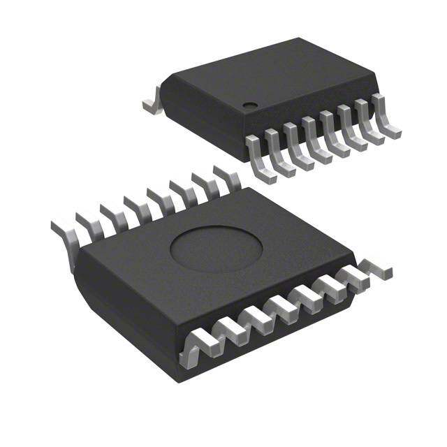
| 产品图片 | |
| 产品型号 | LTC4228IGN-2#PBF |
| rohs | 无铅 / 符合限制有害物质指令(RoHS)规范要求 |
| 产品系列 | - |
| 供应商器件封装 | 28-SSOP |
| 其它名称 | LTC4228IGN2PBF |
| 内部开关 | 无 |
| 功能引脚 | CPO1, CPO2, /EN1, /EN2, /FAULT1, /FAULT2, IN1, IN2, INTVCC, ON1, ON2, OUT1, OUT2, /PWERGD1, /PWRGD2, TMR1, TMR2 |
| 包装 | 管件 |
| 参考设计库 | http://www.digikey.com/rdl/4294959902/4294959901/1224 |
| 可编程特性 | 限流,故障超时,压摆率 |
| 安装类型 | 表面贴装 |
| 封装/外壳 | 28-SSOP(0.154",3.90mm 宽) |
| 工作温度 | -40°C ~ 85°C |
| 应用 | 通用 |
| 标准包装 | 49 |
| 特性 | 自动重试,UVLO |
| 电压-电源 | 2.9 V ~ 18 V |
| 电流-电源 | 2.5mA |
| 电流-输出(最大值) | - |
| 类型 | 热交换控制器, OR 控制器 |
| 通道数 | 2 |
| 配用 | /product-detail/zh/DC1899A-B/DC1899A-B-ND/3903846/product-detail/zh/DC1899A-A/DC1899A-A-ND/3903845 |


- 商务部:美国ITC正式对集成电路等产品启动337调查
- 曝三星4nm工艺存在良率问题 高通将骁龙8 Gen1或转产台积电
- 太阳诱电将投资9.5亿元在常州建新厂生产MLCC 预计2023年完工
- 英特尔发布欧洲新工厂建设计划 深化IDM 2.0 战略
- 台积电先进制程称霸业界 有大客户加持明年业绩稳了
- 达到5530亿美元!SIA预计今年全球半导体销售额将创下新高
- 英特尔拟将自动驾驶子公司Mobileye上市 估值或超500亿美元
- 三星加码芯片和SET,合并消费电子和移动部门,撤换高东真等 CEO
- 三星电子宣布重大人事变动 还合并消费电子和移动部门
- 海关总署:前11个月进口集成电路产品价值2.52万亿元 增长14.8%


PDF Datasheet 数据手册内容提取
LTC4228-1/LTC4228-2 Dual Ideal Diode and Hot Swap Controller FeaTures DescripTion n Power Path and Inrush Current Control for The LTC®4228 offers ideal diode and Hot Swap™ functions Redundant Supplies for two power rails by controlling two external N-channel n Low Loss Replacement for Power Schottky Diodes MOSFETs in each rail. MOSFETs acting as ideal diodes re- n Protects Output Voltage from Input Brownouts place two high power Schottky diodes and the associated n Allows Safe Hot Swapping from a Live Backplane heat sinks, saving power and board area. Hot Swap control n 2.9V to 18V Operating Range MOSFETs allow boards to be safely inserted and removed n Controls N-Channel MOSFETs from a live backplane by limiting inrush current. The supply n Limits Peak Fault Current in ≤1µs output is also protected against short-circuit faults with a n Adjustable Current Limit with Circuit Breaker fast acting current limit and internal timed circuit breaker. n Adjustable Current Limit Fault Delay The LTC4228 regulates the forward voltage drop across n Smooth Switchover without Oscillation the external MOSFETs and sense resistor to ensure smooth n 0.5µs Ideal Diode Turn-On and Turn-Off Time current transfer from one supply to the other without n Status, Fault and Power Good Outputs oscillation. The ideal diodes turn on quickly to reduce n LTC4228-1: Latch Off After Fault the load voltage droop during supply switch-over. If the n LTC4228-2: Automatic Retry After Fault input supply fails or is shorted, a fast turn-off minimizes n 28-Lead 4mm × 5mm QFN and SSOP Packages reverse-current transients. applicaTions The LTC4228 allows independent on/off control, and reports fault and power good status for the supply. The LTC4228 n Redundant Power Supplies improves on the LTC4225 by recovering more quickly from n MicroTCA Systems and Servers input brownouts to preserve the output voltage. n Telecom Networks L, LT, LTC, LTM, Linear Technology and the Linear logo are registered trademarks of Linear n Power Prioritizer Technology Corporation. Hot Swap is a trademark of Linear Technology Corporation. All other trademarks are the property of their respective owners. Typical applicaTion µTCA Application PLUG-IN CARD 1 Smooth Supply Switchover Si7336ADP 0.004Ω Si7336ADP 12V 12V 7.6A 0.1µF CPO1 IN1 DGATE1 SENSE1+ SENSE1– HGATE1 OUT1 IN1 1V/DIV STATUS1 137k FAULT1 PWRGD1 IN2 ON1 EN1 1V/DIV 20k 47nF 0.1µF INTVCC LTC4228 TMR1 47nF PLUG-IN 2A/IDINIV1 GND TMR2 CARD 2 EN2 20k PWRGD2 IIN2 ON2 FAULT2 2A/DIV STATUS2 137k CPO2 IN2 DGATE2 SENSE2+ SENSE2– HGATE2 OUT2 200ms/DIV 422512 TA01b 0.1µF 12V 12V Si7336ADP 0.004Ω Si7336ADP 7.6A BACKPLANE 422812 TA01a 422812f 1
LTC4228-1/LTC4228-2 absoluTe MaxiMuM raTings (Notes 1, 2) Supply Voltages HGATE1, HGATE2 (Note 4) .....................–0.3V to 35V IN1, IN2 ..................................................–0.3V to 24V OUT1, OUT2 ...........................................–0.3V to 24V INTV .....................................................–0.3V to 7V Average Currents CC Input Voltages FAULT1, FAULT2, PWRGD1, PWRGD2 ...................5mA ON1, ON2, EN1, EN2...............................–0.3V to 24V STATUS1, STATUS2 ..............................................5mA TMR1, TMR2 .........................–0.3V to INTV + 0.3V INTV .................................................................1mA CC CC SENSE1+, SENSE2+ ................................–0.3V to 24V Operating Temperature Range SENSE1–, SENSE2–................................–0.3V to 24V LTC4228C ................................................0°C to 70°C Output Voltages LTC4228I .............................................–40°C to 85°C FAULT1, FAULT2, PWRGD1, PWRGD2 .....–0.3V to 24V Storage Temperature Range ..................–65°C to 150°C STATUS1, STATUS2 ................................–0.3V to 24V Lead Temperature (Soldering, 10 sec) CPO1, CPO2 (Note 3) .............................–0.3V to 35V GN Package ......................................................300°C DGATE1, DGATE2 (Note 3) .....................–0.3V to 35V pin conFiguraTion TOP VIEW TOP VIEW 1 S1 1 D1 STATUS1 1 28 HGATE1 GATE PO1 TATU GATE UT1 WRG CPO1 2 27 OUT1 D C S H O P 28 27 26 25 24 23 DGATE1 3 26 PWRGD1 SENSE1– 1 22 FAULT1 SENSE1– 4 25 FAULT1 SENSE1+ 2 21 ON1 SENSE1+ 5 24 ON1 IN1 3 20 EN1 IN1 6 23 EN1 INTVCC 4 29 19 TMR1 INTVCC 7 22 TMR1 GND 5 18 TMR2 GND 8 21 TMR2 IN2 6 17 EN2 IN2 9 20 EN2 SENSE2+ 7 16 ON2 SENSE2+ 10 19 ON2 SENSE2– 8 15 FAULT2 SENSE2– 11 18 FAULT2 9 10 11 12 13 14 DGATE2 12 17 PWRGD2 2 2 2 2 2 2 E O S E T D DGAT CP STATU HGAT OU PWRG STACTPUOS22 1134 1165 OHUGTA2TE2 UFD PACKAGE 28-LEAD (4mm × 5mm) PLASTIC QFN GN PACKAGE 28-LEAD PLASTIC SSOP NARROW TJMAX = 125°C, θJA = 43°C/W (NOTE 5) EXPOSED PAD (PIN 29) PCB GND CONNECTION OPTIONAL TJMAX = 125°C, θJA = 80°C/W 422812f 2
LTC4228-1/LTC4228-2 orDer inForMaTion LEAD FREE FINISH TAPE AND REEL PART MARKING* PACKAGE DESCRIPTION TEMPERATURE RANGE LTC4228CUFD-1#PBF LTC4228CUFD-1#TRPBF 42281 28-Lead (4mm × 5mm) Plastic QFN 0°C to 70°C LTC4228CUFD-2#PBF LTC4228CUFD-2#TRPBF 42282 28-Lead (4mm × 5mm) Plastic QFN 0°C to 70°C LTC4228IUFD-1#PBF LTC4228IUFD-1#TRPBF 42281 28-Lead (4mm × 5mm) Plastic QFN –40°C to 85°C LTC4228IUFD-2#PBF LTC4228IUFD-2#TRPBF 42282 28-Lead (4mm × 5mm) Plastic QFN –40°C to 85°C LTC4228CGN-1#PBF LTC4228CGN-1#TRPBF LTC4228GN-1 28-Lead Plastic SSOP 0°C to 70°C LTC4228CGN-2#PBF LTC4228CGN-2#TRPBF LTC4228GN-2 28-Lead Plastic SSOP 0°C to 70°C LTC4228IGN-1#PBF LTC4228IGN-1#TRPBF LTC4228GN-1 28-Lead Plastic SSOP –40°C to 85°C LTC4228IGN-2#PBF LTC4228IGN-2#TRPBF LTC4228GN-2 28-Lead Plastic SSOP –40°C to 85°C Consult LTC Marketing for parts specified with wider operating temperature ranges. *The temperature grade is identified by a label on the shipping container. Consult LTC Marketing for information on non-standard lead based finish parts. For more information on lead free part marking, go to: http://www.linear.com/leadfree/ For more information on tape and reel specifications, go to: http://www.linear.com/tapeandreel/ elecTrical characTerisTics The l denotes the specifications which apply over the full operating temperature range, otherwise specifications are at T = 25°C. V = 12V, unless otherwise noted. A IN SYMBOL PARAMETER CONDITIONS MIN TYP MAX UNITS Supplies V Input Supply Range l 2.9 18 V IN I Input Supply Current l 2.5 5 mA IN V Internal Regulator Voltage I = 0, –500µA l 4.5 5 5.6 V INTVCC V Internal V Undervoltage Lockout INTV Rising l 2.1 2.2 2.3 V INTVCC(UVL) CC CC ∆VINTVCC(HYST) Internal VCC Undervoltage Lockout Hysteresis l 30 60 90 mV Ideal Diode Control ∆VFWD(REG) Forward Regulation Voltage (VINn – VOUTn) l 10 25 40 mV ∆VDGATE External N-Channel Gate Drive IN < 7V, ∆VFWD = 0.1V, I = 0, –1µA l 5 7 14 V (VDGATEn – VINn) IN = 7V to 18V, ∆VFWD = 0.1V, I = 0, –1µA l 10 12 14 V ∆VDGATE(ST) Diode MOSFET On Detect Threshold STATUS Pulls Low, ∆VFWD = 50mV l 0.3 0.7 1.1 V I CPOn Pull-Up Current CPO = IN = 2.9V l –60 –95 –120 µA CPO(UP) CPO = IN = 18V l –50 –85 –110 µA IDGATE(FPU) DGATEn Fast Pull-Up Current ∆VFWD = 0.2V, ∆VDGATE = 0V, CPO = 17V –1.5 A IDGATE(FPD) DGATEn Fast Pull-Down Current ∆VFWD = –0.2V, ∆VDGATE = 5V 1.5 A tON(DGATE) DGATEn Turn-On Delay ∆VFWD = 0.2V, CDGATE = 10nF l 0.25 0.5 µs tOFF(DGATE) DGATEn Turn-Off Delay ∆VFWD = –0.2V, CDGATE = 10nF l 0.2 0.5 µs Hot Swap Control ∆VSENSE(CB) Circuit Breaker Trip Sense Voltage l 47.5 50 52.5 mV (V + – V –) SENSEn SENSEn ∆VSENSE(ACL) Active Current Limit Sense Voltage l 55 65 75 mV (V + – V –) SENSEn SENSEn V + SENSEn+ Undervoltage Lockout SENSE+ Rising l 1.75 1.9 2.05 V SENSE (UVL) ∆VSENSE+(HYST) SENSEn+ Undervoltage Lockout Hysteresis l 10 50 90 mV I + SENSEn+ Input Current SENSE+ = 12V l 150 350 500 µA SENSE I – SENSEn– Input Current SENSE– = 12V l 10 50 100 µA SENSE ∆VHGATE External N-Channel Gate Drive IN < 7V, I = 0, –1µA l 4.8 7 14 V (V – V ) IN = 7V to 18V, I = 0, –1µA l 10 12 14 V HGATEn OUTn 422812f 3
LTC4228-1/LTC4228-2 elecTrical characTerisTics The l denotes the specifications which apply over the full operating temperature range, otherwise specifications are at T = 25°C. V = 12V, unless otherwise noted. A IN SYMBOL PARAMETER CONDITIONS MIN TYP MAX UNITS ∆VHGATE(PG) Gate-Source Voltage for Power Good l 3.6 4.2 4.8 V I External N-Channel Gate Pull-Up Current Gate Drive On, HGATE = 0V l –7 –10 –13 µA HGATE(UP) I External N-Channel Gate Pull-Down Current Gate Drive Off, OUT = 12V, l 150 300 500 µA HGATE(DN) HGATE = OUT + 5V I External N-Channel Gate Fast Fast Turn-Off, OUT = 12V, l 100 200 300 mA HGATE(FPD) Pull-Down Current HGATE = OUT + 5V tPHL(SENSE) Sense Voltage (SENSEn+ – SENSEn–) ∆VSENSE = 300mV, CHGATE = 10nF l 0.5 1 µs High to HGATEn Low t ENn High to HGATEn Low l 20 40 µs OFF(HGATE) ONn Low to HGATEn Low l 10 20 µs SENSEn+ Low to HGATEn Low l 10 20 µs t ONn High, ENn Low to HGATEn l 50 100 150 ms D(HGATE) Turn-On Delay t ONn to HGATEn Propagation Delay ON = Step 0.8V to 2V l 10 20 µs P(HGATE) Input/Output Pin V ONn Threshold Voltage ON Rising l 1.21 1.235 1.26 V ON(TH) ∆VON(HYST) ONn Hysteresis l 40 80 140 mV V ONn Fault Reset Threshold Voltage ON Falling l 0.55 0.6 0.63 V ON(RESET) I ONn Input Leakage Current ON = 5V l 0 ±1 µA ON(LEAK) V ENn Threshold Voltage EN Rising l 1.185 1.235 1.284 V EN(TH) ∆VEN(HYST) ENn Hysteresis l 40 130 200 mV I ENn Pull-Up Current EN = 1V l –7 –10 –13 µA EN(UP) V TMRn Threshold Voltage TMR Rising l 1.198 1.235 1.272 V TMR(TH) TMR Falling l 0.15 0.2 0.25 V I TMRn Pull-Up Current TMR = 1V, In Fault Mode l –75 –100 –125 µA TMR(UP) I TMRn Pull-Down Current TMR = 2V, No Faults l 1.4 2 2.6 µA TMR(DN) I TMRn Current Ratio I /I l 1.4 2 2.7 % TMR(RATIO) TMR(DN) TMR(UP) I OUTn Current OUT = 11V, IN = 12V, ON = 2V l 50 120 µA OUT OUT = 13V, IN = 12V, ON = 2V l 2.5 5 mA V Output Low Voltage I = 1mA l 0.15 0.4 V OL (FAULTn, PWRGDn, STATUSn) V Output High Voltage I = –1µA l INTV – 1 INTV – 0.5 V OH CC CC (FAULTn, PWRGDn, STATUSn) I Input Leakage Current V = 18V l 0 ±1 µA OH (FAULTn, PWRGDn, STATUSn) I Output Pull-Up Current V = 1.5V l –7 –10 –13 µA PU (FAULTn, PWRGDn, STATUSn) t ONn Low to FAULTn High l 20 40 µs RST(ON) Note 1: Stresses beyond those listed under Absolute Maximum Ratings Note 3: An internal clamp limits the DGATE and CPO pins to a minimum of may cause permanent damage to the device. Exposure to any Absolute 10V above and a diode below IN. Driving these pins to voltages beyond the Maximum Rating condition for extended periods may affect device clamp may damage the device. reliability and lifetime. Note 4: An internal clamp limits the HGATE pin to a minimum of 10V Note 2: All currents into device pins are positive; all currents out of device above and a diode below OUT. Driving this pin to voltages beyond the pins are negative. All voltages are referenced to GND unless otherwise clamp may damage the device. specified. Note 5: Thermal resistance is specified when the exposed pad is soldered to a 3" × 4.5", four layer, FR4 board. 422812f 4
LTC4228-1/LTC4228-2 Typical perForMance characTerisTics T = 25°C, V = 12V, unless otherwise noted. A IN IN Supply Current vs Voltage INTV Load Regulation CPO Voltage vs Current CC 4 6 12 5 VIN = 12V 10 3 V) 8 I (mA)IN 2 INTV (V)CC 234 VIN = 3.3V – V (∆V) (POINCPO 64 VIN = 2.9VVIN = 18V 1 VC 2 1 0 0 0 –2 0 3 6 9 12 15 18 0 –2 –4 –6 –8 –10 0 –20 –40 –60 –80 –100 –120 VIN (V) ILOAD (mA) ICPO (µA) 422812 G01 422812 G02 422812 G03 Diode Gate Voltage vs Current Hot Swap Gate Voltage vs Current OUT Current vs Voltage 12 14 3.0 VOUT = VIN – 0.1V VOUT = VIN VIN = 12V 10 12 VIN = 12V 2.5 V) V) ∆V) (DGATE 86 VIN = 18V ∆V) (HGATE 108 mA) 12..50 – V (IN 4 RIVE ( 6 VIN = 2.9V I (OUT 1.0 V DGATE 2 VIN = 2.9V GATE D 4 0.5 0 2 0 –2 0 –0.5 0 –20 –40 –60 –80 –100 –120 0 –2 –4 –6 –8 –10 –12 0 3 6 9 12 15 18 IDGATE (µA) IHGATE (µA) VOUT (V) 422812 G04 422812 G05 422812 G06 Circuit Breaker Trip Voltage Active Current Limit Sense Active Current Limit Delay vs Temperature Voltage vs Temperature vs Sense Voltage 52 mV) 67 100 CHGATE = 10nF mV) GE ( s) P VOLTAGE ( 51 ENSE VOLTA 66 MIT DELAY (µ 10 R TRI 50 MIT S 65 NT LI CIRCUIT BREAKE 49 TIVE CURRENT LI 64 ACTIVE CURRE 1 C 48 A 63 0.1 –50 –25 0 25 50 75 100 –50 –25 0 25 50 75 100 50 100 150 200 250 300 TEMPERATURE (°C) TEMPERATURE (°C) SENSE VOLTAGE (VIN – VSENSE) (mV) 422812 G07 422812 G08 422812 G09 422812f 5
LTC4228-1/LTC4228-2 Typical perForMance characTerisTics T = 25°C, V = 12V, unless otherwise noted. A IN HGATE Pull-Up Current TMR Pull-Up Current PWRGD, FAULT, STATUS Output vs Temperature vs Temperature Low Voltage vs Current –11.0 –103 0.8 NT (µA)–10.5 T (µA)–102 E (V) 0.6 E N–101 G R E A UP CUR–10.0 P CURR–100 W VOLT 0.4 HGATE PULL- –9.5 TMR PULL-U––9989 OUTPUT LO 0.2 –9.0 –97 0 –50 –25 0 25 50 75 100 –50 –25 0 25 50 75 100 0 1 2 3 4 5 TEMPERATURE (°C) TEMPERATURE (°C) CURRENT (mA) 422812 G10 422812 G11 422812 G12 pin FuncTions CPO1, CPO2: Charge Pump Output. Connect a capacitor FAULT1, FAULT2: Fault Status Output. Open-drain output from CPO1 or CPO2 to the corresponding IN1 or IN2 pin. that is normally pulled high by a 10µA current source to a The value of this capacitor is approximately 10× the gate diode below INTV . It may be pulled above INTV using CC CC capacitance (C ) of the external MOSFET for ideal diode an external pull-up. It pulls low when the circuit breaker ISS control. The charge stored on this capacitor is used to pull is tripped after an overcurrent fault timeout. Leave open up the gate during a fast turn-on. Leave this pin open if if unused. fast turn-on is not needed. GND: Device Ground. DGATE1, DGATE2: Ideal Diode MOSFET Gate Drive Out- HGATE1, HGATE2: Hot Swap MOSFET Gate Drive Output. put. Connect this pin to the gate of an external N-channel Connect this pin to the gate of the external N-channel MOSFET for ideal diode control. An internal clamp limits MOSFET for Hot Swap control. An internal 10µA current the gate voltage to 12V above and a diode voltage below source charges the MOSFET gate. An internal clamp limits IN. During fast turn-on, a 1.5A pull-up charges DGATE from the gate voltage to 12V above and a diode below OUT. CPO. During fast turn-off, a 1.5A pull-down discharges During turn-off, a 300µA pull-down discharges HGATE to DGATE to IN. ground. During an output short or INTV undervoltage CC EN1, EN2: Enable Input. Ground this pin to enable Hot lockout, a fast 200mA pull-down discharges HGATE to OUT. Swap control. If this pin is pulled high, the MOSFET is not IN1, IN2: Positive Supply Input and Ideal Diode’s MOSFET allowed to turn on. A 10µA current source pulls this pin Gate Drive Return. The 5V INTV supply is generated CC up to a diode below INTV . Upon EN going low when ON CC from IN1, IN2, OUT1 and OUT2 via an internal diode-OR. is high, an internal timer provides a 100ms start-up delay The voltage sensed at this pin is used to control DGATE for debounce, after which the fault is cleared. for forward voltage regulation and reverse turn-off. The Exposed Pad (UFD Package): The exposed pad may be gate fast pull-down current returns through this pin when left open or connected to device ground. DGATE is discharged. 422812f 6
LTC4228-1/LTC4228-2 pin FuncTions INTV : Internal 5V Supply Decoupling Output. This pin at this pin is used for monitoring the current limit. This CC must have a 0.1µF or larger capacitor. An external load of pin has an undervoltage lockout threshold of 1.9V that less than 500µA can be connected at this pin. will turn off the Hot Swap MOSFET. ON1, ON2: On Control Input. A rising edge above 1.235V SENSE1–, SENSE2–: Negative Current Sense Input. Con- turns on the external Hot Swap MOSFET and a falling edge nect this pin to the output of the current sense resistor. below 1.155V turns it off. Connect this pin to an external The current limit circuit controls HGATE to limit the voltage resistive divider from IN or SENSE+ to monitor the supply between SENSE+ and SENSE– to 65mV. A circuit breaker undervoltage condition. Pulling the ON pin below 0.6V trips when the sense voltage exceeds 50mV for more than resets the electronic circuit breaker. a fault filter delay configured at the TMR pin. OUT1, OUT2: Output Voltage Sense and Hot Swap’s MOS- STATUS1, STATUS2: Diode MOSFET Status Output. FET Gate Drive Return. Connect this pin to the output side Open-drain output that is normally pulled high by a 10µA of the external MOSFET. The voltage sensed at this pin is current source to a diode below INTV . It may be pulled CC used to control DGATE. The gate fast pull-down current above INTV using an external pull-up. It pulls low when CC returns through this pin when HGATE is discharged. the MOSFET gate drive between DGATE and IN exceeds the gate-to-source voltage of 0.7V. Leave open if unused. PWRGD1, PWRGD2: Power Status Output. Open-drain output that is normally pulled high by a 10µA current TMR1, TMR2: Timer Capacitor Terminal. Connect a capaci- source to a diode below INTV . It may be pulled above tor between this pin and ground to set a 12ms/µF duration CC INTV using an external pull-up. It pulls low when the for current limit before the external Hot Swap MOSFET CC MOSFET gate drive between HGATE and OUT exceeds is turned off. The duration of the off time is 617ms/µF, the gate-to-source voltage of 4.2V. Leave open if unused. resulting in a 2% duty cycle. SENSE1+, SENSE2+: Positive Current Sense Input. Connect this pin to the output of the external ideal diode MOSFET and input of the current sense resistor. The voltage sensed 422812f 7
LTC4228-1/LTC4228-2 block DiagraM SENSE1+ SENSE1– SENSE2– SENSE2+ HGATE1 65mV 50mV 50mV 65mV HGATE2 + –+ +– + + –+ +– + A1 ECB1 ECB2 A2 12V – – – – 12V IN1 IN2 10µA 10µA CHARGE CHARGE 100µA PUMP 1 PUMP 2 100µA CPO1 f = 2MHz f = 2MHz CPO2 INTVCC INTVCC GATE GATE DRIVER 1 + 5V LDO + DRIVER 2 DGATE1 DGATE2 GA1 GA2 – +– –+ – 12V 12V 25mV 25mV OUT1 OUT2 2.2V INTVCC – PG1 – + INTVCC UV3 HGATE1 +– + PG2 – 4.2VSENSE1+ +UV1 UV2 + SENSE2+ + –+ HGATE2 4.2V 0.7V 1.9V – – 1.9V 0.7V DGATE1 +– + STAT1 STAT2 + –+ DGATE2 IN1 – – IN2 1.235V –CP1 HGATE1 ON HGATE2 ON CP3 – 1.235V + + ON1 ON2 INTVCC – CP2 FAULT1 RESET FAULT2 RESET CP4 – INTVCC 0.6V + + 0.6V 10µA 10µA EN1 + CP5 CP6 + EN2 CARD1 PRESENCE DETECT CARD2 PRESENCE DETECT 1.235V – – 1.235V INTVCC INTVCC 100µA 100µA 1.235V – CP7 CP9 – 1.235V LOGIC + + TMR1 TMR2 – CP8 CP10 – 0.2V + + 0.2V 2µA 2µA INTVCC INTVCC INTVCC INTVCC INTVCC INTVCC 10µA 10µA 10µA 10µA 10µA 10µA STATUS1 STATUS2 FAULT1 FAULT2 PWRGD1 PWRGD2 GND EXPOSED PAD* *UFD PACKAGE ONLY 422812 BD 422812f 8
LTC4228-1/LTC4228-2 operaTion The LTC4228 functions as an ideal diode with inrush cur- When both of the MOSFETs are turned on, the gate drive rent limiting and overcurrent protection by controlling two amplifier controls DGATE to servo the forward voltage external N-channel MOSFETs (M and M ) on a supply drop (V – V ) across the sense resistor and the two D H IN OUT path. This allows boards to be safely inserted and removed MOSFETs to 25mV. If the load current causes more than in systems with a backplane powered by redundant sup- 25mV of voltage drop, the DGATE voltage rises to enhance plies, such as µTCA applications. The LTC4228 has two the MOSFET used for ideal diode control. For large output separate ideal diode and Hot Swap controllers, each currents, the ideal diode MOSFET is driven fully on and providing independent control for the two input supplies. the voltage drop across the MOSFETs is equal to the sum of the I • R of the two MOSFETs in series. When the LTC4228 is first powered up, the gates of the LOAD DS(ON) external MOSFETs are held low, keeping them off. The gate In the case of an input supply short circuit when the drive amplifier (GA1, GA2) monitors the voltage between the MOSFETs are conducting, a large reverse current starts IN and OUT pins and drives the DGATE pin. The amplifier flowing from the load towards the input. The gate drive quickly pulls up the DGATE pin, turning on the MOSFET amplifier detects this failure condition as soon as it ap- for ideal diode control, when it senses a large forward pears and turns off the ideal diode MOSFET by pulling voltage drop. The stored charge in an external capacitor down the DGATE pin. connected between the CPO and IN pins provides the In the case where an overcurrent fault occurs on the sup- charge needed to quickly turn on the ideal diode MOSFET. ply output, the current is limited to 65mV/R . After a fault S An internal charge pump charges up this capacitor at device filter delay set by 100µA charging the TMR pin capacitor, power-up. The DGATE pin sources current from the CPO the circuit breaker trips and pulls the HGATE pin low, turn- pin and sinks current into the IN and GND pins. When the ing off the Hot Swap MOSFET. Only the supply at fault is DGATE to IN voltage exceeds 0.7V, the STATUS pin pulls affected, with the corresponding FAULT pin latched low. low to indicate that the ideal diode MOSFET is turned on. At this point, the DGATE pin continues to pull high and Pulling the ON pin high and the EN pin low initiates a keeps the ideal diode MOSFET on. 100ms debounce timing cycle. After this timing cycle, Internal clamps limit both the DGATE to IN and CPO to IN a 10µA current source from the charge pump ramps up voltages to 12V. The same clamp also limits the CPO and the HGATE pin. When the Hot Swap MOSFET turns on, DGATE pins to a diode voltage below the IN pin. Another the inrush current is limited at a level set by an external internal clamp limits the HGATE to OUT voltage to 12V sense resistor (R ) connected between the SENSE+ and S and also clamps the HGATE pin to a diode voltage below SENSE– pins. An active current limit amplifier (A1, A2) the OUT pin. servos the gate of the MOSFET to 65mV across the current sense resistor. Inrush current can be further reduced, if Power to the LTC4228 is supplied from either the IN or desired, by adding a capacitor from HGATE to GND. When OUT pins, through an internal diode-OR circuit to a low the MOSFET ’s gate overdrive (HGATE to OUT voltage) dropout regulator (LDO). That LDO generates a 5V supply exceeds 4.2V, the PWRGD pin pulls low. at the INTVCC pin and powers the LTC4228’s internal low voltage circuitry. 422812f 9
LTC4228-1/LTC4228-2 applicaTions inForMaTion High availability systems often employ parallel-connected internally regulated at 5V by a low dropout regulator (LDO) power supplies or battery feeds to achieve redundancy with an output at the INTV pin. An internal diode-OR CC and enhance system reliability. Power ORing diodes are circuit selects the highest of the supplies at the IN and OUT commonly used to connect these supplies at the point of pins to power the device through the LDO. The diode-OR load, but at the expense of power loss due to significant scheme permits the device’s power to be temporarily kept diode forward voltage drop. The LTC4228 minimizes this alive by the OUT load capacitance when the IN supplies power loss by using external N-channel MOSFETs for the have collapsed or shut off. pass elements, allowing for a low voltage drop from the An undervoltage lockout circuit prevents all of the MOSFETs supply to the load when the MOSFETs are turned on. When from turning on until the INTV voltage exceeds 2.2V. A CC an input source voltage drops below the output common 0.1µF capacitor is recommended between the INTV and CC supply voltage, the appropriate MOSFET is turned off, GND pins, close to the device for bypassing. No external thereby matching the function and performance of an ideal supply should be connected at the INTV pin so as not CC diode. By adding a current sense resistor in between the to affect the LDO’s operation. A small external load of less two external MOSFETs that are separately controlled, the than 500µA can be connected at the INTV pin. CC LTC4228 enhances the ideal diode performance with inrush current limiting and overcurrent protection (see Figure 1). Turn-On Sequence This allows the boards to be safely inserted and removed The board power supply at the OUT pin is controlled with from a live backplane without damaging the connector. two external N-channel MOSFETs (M , M ). The MOSFET D H Internal VCC Supply MD on the supply side functions as an ideal diode, while M on the load side acts as a Hot Swap controlling the H The LTC4228 can operate with input supplies from 2.9V power supplied to the output load. The sense resistor, R , S to 18V at the IN pins. The power supply to the device is PLUG-IN MD1 RS1 MH1 CARD 1 Si7336ADP 0.004Ω Si7336ADP 12V V1I2NV1 BULK 7.6A SUPPLY BYPASS RH1 RHG1 CAPACITOR CCP1 10Ω 47Ω 0.1µF CHG1 15nF VSENSE1+ + CL1 CPO1 IN1 DGATE1 SENSE1+ SENSE1– HGATE1 OUT1 1600µF R5 R6 R7 100k 100k 100k R2 137k STATUS1 ON1 FAULT1 R1 CF1 PWRGD1 20k 10nF EN1 C1 INTVCC TMR1 0.1µF GND LTC4228 TMR2 C47Tn2F C47T1nF PCLAURGD- I2N R203k C10F2nF PWRGEND22 ON2 FAULT2 R4 STATUS2 137k R8 R9 R10 CPO2 IN2 DGATE2 SENSE2+ SENSE2– HGATE2 OUT2 100k 100k 100k CL2 +1600µF CCP2 R10HΩ2 R47HΩG2 VSENSE2+ 0.1µF CHG2 15nF V1I2NV2 BULK MD2 RS2 MH2 172.6VA SUPPLY Si7336ADP 0.004Ω Si7336ADP BACKPLANE 422812 F01 BYPASS CAPACITOR Figure 1. µTCA Application Supplying 12V Power to Two µTCA Slots 422812f 10
LTC4228-1/LTC4228-2 applicaTions inForMaTion monitors the load current for overcurrent detection. The Turn-Off Sequence HGATE capacitor, C , controls the gate slew rate to limit HG The external MOSFETs can be turned off by a variety of the inrush current. Resistor R with C compensates HG HG conditions. A normal turn-off for the Hot Swap MOSFET is the current control loop, while R prevents high frequency H initiated by pulling the ON pin below its 1.155V threshold oscillations in the Hot Swap MOSFET. (80mV ON pin hysteresis), or pulling the EN pin above During a normal power-up, the ideal diode MOSFET turns its 1.235V threshold. Additionally, an overcurrent fault on first. As soon as the internally generated supply, INTV , of sufficient duration to trip the circuit breaker also turns CC rises above its 2.2V undervoltage lockout threshold, the off the Hot Swap MOSFET. Normally, the LTC4228 turns internal charge pump is allowed to charge up the CPO off the MOSFET by pulling the HGATE pin to ground with pins. Because the Hot Swap MOSFET is turned off at a 300µA current sink. power-up, OUT remains low. As a result, the ideal diode All of the MOSFETs turn off when INTV falls below its CC gate drive amplifier senses a large forward drop between undervoltage lockout threshold (2.2V). The DGATE pin is the IN and OUT pins, causing it to pull up DGATE to the pulled down with a 100µA current to one diode voltage CPO pin voltage. below the IN pin, while the HGATE pin is pulled down to Before the Hot Swap MOSFET can be turned on, EN must the OUT pin by a 200mA current. remain low and ON must remain high for a 100ms debounce The gate drive amplifier controls the ideal diode MOSFET cycle to ensure that any contact bounces during the inser- to prevent reverse current when the input supply falls tion have ceased. At the end of the debounce cycle, the below OUT. If the input supply collapses quickly, the gate internal fault latches are cleared. The Hot Swap MOSFET drive amplifier turns off the ideal diode MOSFET with a is then allowed to turn on by charging up HGATE with a fast pull-down circuit as soon as it detects that IN is 20mV 10µA current source from the charge pump. The voltage at the HGATE pin rises with a slope equal to 10µA/C and HG the supply inrush current flowing into the load capacitor, IN C , is limited to: 10V/DIV L C CPO I = L •10µA 10V/DIV INRUSH C HG DGATE 10V/DIV The OUT voltage follows the HGATE voltage when the OUT Hot Swap MOSFET turns on. If the voltage across the 10V/DIV current sense resistor, RS, becomes too high, the inrush 20ms/DIV 422812 F02 current will be limited by the internal current limiting Figure 2. Ideal Diode Controller Start-Up Waveforms circuitry. Once the MOSFET gate overdrive exceeds 4.2V, the corresponding PWRGD pin pulls low to indicate that the power is good. Once OUT reaches the input supply ON 5V/DIV voltage, HGATE continues to ramp up. An internal 12V clamp limits the HGATE voltage above OUT. HGATE 10V/DIV When both of the MOSFETs are turned on, the gate drive OUT 10V/DIV amplifier controls the gate of the ideal diode MOSFET, to PWRGD servo its forward voltage drop across R , M and M to S D H 10V/DIV 25mV. If the load current causes more than 25mV of drop, the MOSFET gate is driven fully on and the voltage drop 50ms/DIV 422812 F03 across the MOSFET is equal to I • R . Figure 3. Hot Swap Controller Power-Up Sequence LOAD DS(ON) 422812f 11
LTC4228-1/LTC4228-2 applicaTions inForMaTion below OUT. If the input supply falls at a more modest rate, period of 14 timing cycles at the TMR pin. For the latch-off the gate drive amplifier controls the MOSFET to maintain part (LTC4228-1), the HGATE pin voltage does not restart OUT at 25mV below IN. at the end of the cool-off period, unless the latched fault is cleared by pulling the ON pin low or toggling the EN Board Presence Detect with EN pin from high to low. For the auto-retry part (LTC4228-2), the latched fault is cleared automatically at the end of the If ON is high when the EN pin goes low, indicating a board cool-off period, and the HGATE pin restarts charging up presence, the LTC4228 initiates a 100ms timing cycle for to turn on the MOSFET. Figure 4 shows an overcurrent contact debounce. Upon board insertion, any bounces fault on the 12V output. on the EN pin restart the timing cycle. When the 100ms timing cycle is done, the internal fault latches are cleared. OUT If the EN pin remains low at the end of the timing cycle, 10V/DIV HGATE is charged up with a 10µA current source to turn HGATE 10V/DIV on the Hot Swap MOSFET. If the EN pin goes high, indicating a board removal, the HGATE pin is pulled low with a 300µA current sink after a 20µs delay, turning off the Hot Swap MOSFET without ILOAD clearing any latched faults. 40A/DIV 100µs/DIV 422812 F04 Overcurrent Fault Figure 4. Overcurrent Fault on 12V Output The LTC4228 features an adjustable current limit with circuit In the event of a severe short-circuit fault on the 12V output breaker function that protects the external MOSFETs against as shown in Figure 5, the output current can surge to tens short circuits or excessive load current. The voltage across of amperes. The LTC4228 responds within 1µs to bring the external sense resistor (R , R ) is monitored by an the current under control by pulling the HGATE to OUT S1 S2 electronic circuit breaker (ECB) and active current limit voltage down to zero volts. Almost immediately, the gate (ACL) amplifier. The electronic circuit breaker will turn off of the Hot Swap MOSFET recovers rapidly due to the R HG the Hot Swap MOSFET with a 300µA current from HGATE and C network, and current is actively limited until the HG to GND if the voltage across the sense resistor exceeds electronic circuit breaker times out. Due to parasitic sup- ∆V (50mV) for longer than the fault filter delay ply lead inductance, an input supply without any bypass SENSE(CB) configured at the TMR pin. capacitor may collapse during the high current surge and then spike upwards when the current is interrupted. Active current limiting begins when the sense voltage Figure 11 shows the input supply transient suppressors exceeds the ACL threshold ∆V (65mV), which SENSE(ACL) consisting of Z1, R , C and Z2, R , C is 1.3× the ECB threshold ∆V . The gate of the SNUB1 SNUB1 SNUB2 SNUB2 SENSE(CB) for the two supplies if there is no input capacitance. Hot Swap MOSFET is brought under control by the ACL amplifier and the output current is regulated to maintain OUT the ACL threshold across the sense resistor. At this point, 10V/DIV the fault filter starts the timeout with a 100µA current HGATE charging the TMR pin capacitor. If the TMR pin voltage 10V/DIV exceeds its threshold (1.235V), the external MOSFET turns off with HGATE pulled to ground by 300µA, and its associated FAULT pulls low. ILOAD 40A/DIV After the Hot Swap MOSFET turns off, the TMR pin ca- pacitor is discharged with a 2µA pull-down current until 2µs/DIV 422812 F05 its threshold reaches 0.2V. This is followed by a cool-off Figure 5. Severe Short-Circuit on 12V Output 422812f 12
LTC4228-1/LTC4228-2 applicaTions inForMaTion Active Current Loop Stability (LTC4228-1). For the auto-retry part (LTC4228-2), the latched fault is cleared automatically following the cool-off The active current loop on the HGATE pin is compensated period and the HGATE pin voltage is allowed to restart. by the parasitic gate capacitance of the external N-channel MOSFET. No further compensation components are nor- Resetting Faults (LTC4228-1) mally required. In the case when a MOSFET with C ≤ ISS 2nF is chosen, an R and C compensation network For the latch-off part (LTC4228-1), an overcurrent fault HG HG connected at the HGATE pin may be required. The value is latched after tripping the circuit breaker, and the cor- of C is selected based on the inrush current allowed for responding FAULT pin is asserted low. If the LTC4228 HG the output load capacitance. The resistor, R , connected controls the MOSFETs on two supplies, only the Hot Swap HG in series with C accelerates the MOSFET gate recovery MOSFET on the supply at fault is turned off and the other HG for active current limiting after a fast gate pull-down due is not affected. to an output short. The value of C should be ≤100nF HG To reset a latched fault and restart the output, pull the and R should be between 10Ω and 100Ω for optimum HG corresponding ON pin below 0.6V for more than 100µs performance. and then high above 1.235V. The fault latches reset and the FAULT pin deasserts on the falling edge of the ON pin. TMR Pin Functions When ON goes high again, a 100ms debounce cycle is An external capacitor, C , connected from the TMR pin to T initiated before the HGATE pin voltage restarts. Toggling GND serves as fault filtering when the supply output is in the EN pin high and then low again also resets a fault, active current limit. When the voltage across the sense but the FAULT pin pulls high at the end of the 100ms resistor exceeds the circuit breaker trip threshold (50mV), debounce cycle before the HGATE pin voltage starts up. TMR pulls up with 100µA. Otherwise, it pulls down with 2µA. Bringing all the supplies below the INTV undervoltage CC The fault filter times out when the 1.235V TMR threshold lockout threshold (2.2V) shuts off all the MOSFETs and is exceeded, causing the corresponding FAULT pin to pull resets all the fault latches. A 100ms debounce cycle is low. The fault filter delay or circuit breaker time delay is: initiated before a normal start-up when any of the supplies tCB = CT • 12[ms/µF] is restored above the INTVCC UVLO threshold. After the circuit breaker timeout, the TMR pin capacitor Auto-Retry After a Fault (LTC4228-2) pulls down with 2µA from the 1.235V TMR threshold until it reaches 0.2V. Then, it completes 14 cooling cycles For the auto-retry part (LTC4228-2), the latched fault is reset consisting of the TMR pin capacitor charging to 1.235V automatically after a cool-off timing cycle as described in with a 100µA current and discharging to 0.2V with a 2µA the TMR Pin Functions section. At the end of the cool-off current. At that point, the HGATE pin voltage is allowed to period, the fault latch is cleared and FAULT pulls high. The start up if the fault has been cleared as described in the HGATE pin voltage is allowed to start up and turn on the Resetting Faults section. When the latched fault is cleared Hot Swap MOSFET. If the output short persists, the supply during the cool-off period, the corresponding FAULT pin powers up into a short with active current limiting until pulls high. The total cool-off time for the MOSFET after the circuit breaker times out and FAULT again pulls low. A an overcurrent fault is: new cool-off cycle begins with TMR ramping down with a 2µA current. The whole process repeats itself until the t = C • 11[s/µF] COOL T output short is removed. Since t and t are a func- CB COOL If the latched fault is not cleared after the cool-off period, tion of TMR capacitance, C , the auto-retry duty cycle is T the cooling cycles continue until the fault is cleared. equal to 0.1%, irrespective of C . T After the cool-off period, the HGATE pin is only allowed to Figure 6 shows an auto-retry sequence after an overcur- pull up if the fault has been cleared for the latch-off part rent fault. 422812f 13
LTC4228-1/LTC4228-2 applicaTions inForMaTion input supplies are restored and INTV exceeds its UVLO CC TMR threshold. 1V/DIV There is a 10µs glitch filter on the ON pin to reject supply ILOAD glitches. By placing a filter capacitor, C , with the resis- 20A/DIV F HGATE tive divider at the ON pin, the glitch filter delay is further 5V/DIV extended by the RC time constant to prevent any false fault. FAULT 10V/DIV Power Good Monitor 50ms/DIV 422812 F06 Internal circuitry monitors the MOSFET gate overdrive Figure 6. Auto-Retry Sequence After a Fault between the HGATE and OUT pins. The power good status for each supply is reported via its respective open-drain Supply Undervoltage Monitor output, PWRGD1 or PWRGD2. They are normally pulled The ON pin functions as a turn-on control and an input sup- high by an external pull-up resistor or the internal 10µA ply monitor. A resistive divider connected between the input pull-up. The power good output asserts low when the gate supply (IN1 or SENSE1+, IN2 or SENSE2+) and GND at the re- overdrive exceeds 4.2V during the HGATE start-up. Once spective ON pin monitors the supply undervoltage condition. asserted low, the power good status is latched and can only The undervoltage threshold is set by proper selection of the be cleared by pulling the ON pin low, toggling the EN pin resistors and is given by: from low to high, or INTV entering undervoltage lockout. CC The power good output continues to pull low while HGATE R V = 1+ TOP •V is regulating in active current limit, but pulls high when IN(UVTH) ON(TH) RBOTTOM the circuit breaker times out and pulls the HGATE pin low. where V is the ON rising threshold (1.235V). ON(TH) CPO and DGATE Start-Up An undervoltage fault occurs if the input supply falls below The CPO and DGATE pin voltages are initially pulled up its undervoltage threshold for longer than 20µs. The FAULT to a diode below the IN pin when first powered up. CPO pin will not be pulled low. If the ON pin voltage falls below starts ramping up 7µs after INTV clears its undervolt- CC 1.155V but remains above 0.6V, the Hot Swap MOSFET is age lockout level. Another 40µs later, DGATE also starts turned off by a 300µA pull-down from HGATE to ground. ramping up with CPO. The CPO ramp rate is determined The Hot Swap MOSFET turns back on instantly without by the CPO pull-up current into the combined CPO and the 100ms debounce cycle when the input supply rises DGATE pin capacitances. An internal clamp limits the CPO above its undervoltage threshold. pin voltage to 12V above the IN pin, while the final DGATE However, if the ON pin voltage drops below 0.6V, it turns pin voltage is determined by the gate drive amplifier. An off the Hot Swap MOSFET and clears the associated fault internal 12V clamp limits the DGATE pin voltage above IN. latches. The Hot Swap MOSFET turns back on only after a MOSFET Selection 100ms debounce cycle when the input supply is restored above its undervoltage threshold. An undervoltage fault on The LTC4228 drives N-channel MOSFETs to conduct the one supply does not affect the operation of the other sup- load current. The important features of the MOSFETs are ply. The ideal diode function controlled by the ideal diode on-resistance, R , the maximum drain-source volt- DS(ON) MOSFET is unaffected by undervoltage fault conditions. age, BV , and the threshold voltage. DSS If both IN supplies fall until the internally generated sup- The gate drive for the ideal diode MOSFET and Hot Swap ply, INTVCC, drops below its 2.2V UVLO threshold, all the MOSFET is guaranteed to be greater than 5V and 4.8V MOSFETs are turned off and the fault latches are cleared. respectively when the supply voltages at IN1 and IN2 are Operation resumes from a fresh start-up cycle when the between 2.9V and 7V. When the supply voltages at IN1 and 422812f 14
LTC4228-1/LTC4228-2 applicaTions inForMaTion IN2 are greater than 7V, the gate drive is guaranteed to be current I , the minimum circuit breaker trip cur- LOAD(MAX) greater than 10V. The gate drive is limited to not more than rent I and the lower limit for the circuit breaker TRIP(MIN) 14V. This allows the use of logic-level threshold N-channel threshold ∆V . A load current margin given SENSE(CB)(MIN) MOSFETs and standard N-channel MOSFETs above 7V. An as a ratio of I /I is provided for allowing TRIP(MIN) LOAD(MAX) external Zener diode can be used to clamp the potential backfeeding current to flow through the sense resistor from the MOSFET’s gate to source if the rated breakdown momentarily, without false tripping the circuit breaker on voltage is less than 14V. the higher supply before the reverse turn-off is activated on the lower supply. Assuming a load current margin of 1.5×, The maximum allowable drain-source voltage, BV , DSS must be higher than the supply voltages as the full sup- I = 1.5 • I = 1.5 • 7.6A = 11.4A TRIP(MIN) LOAD(MAX) ply voltage can appear across the MOSFET. If an input or ∆V 47.5mV output is connected to ground, the full supply voltage will R = SENSE(CB)(MIN) = =4.16mΩ S appear across the MOSFET. The R should be small I 11.4A DS(ON) TRIP(MIN) enough to conduct the maximum load current, and also stay within the MOSFET ’s power rating. Choose a 4mΩ sense resistor with a 1% tolerance. Next, calculate the R of the MOSFET to achieve DS(ON) CPO Capacitor Selection the desired forward drop at maximum load. Assuming The recommended value of the capacitor, C , between the a forward drop, ∆V of 60mV across the two external CP FWD CPO and IN pins is approximately 10× the input capaci- MOSFETs: tance, C , of the ideal diode MOSFET. A larger capacitor ISS ∆V 60mV takes a correspondingly longer time to charge up by the R ≤ FWD = =7.9mΩ DS(ON,TOTAL) I 7.6A internal charge pump. A smaller capacitor suffers more LOAD(MAX) voltage drop during a fast gate turn-on event as it shares The Si7336ADP offers a good choice with a maximum charge with the MOSFET gate capacitance. R of 3mΩ at V = 10V, thereby giving a total of DS(ON) GS 6mΩ for two MOSFETs in the supply path. The input ca- Supply Transient Protection pacitance, C , of the Si7336ADP is about 5600pF. Slightly ISS When the capacitances at the input and output are very exceeding the 10× recommendation, a 0.1µF capacitor is small, rapid changes in current during input or output short- selected for C and C at the CPO pins. CP1 CP2 circuit events can cause transients that exceed the 24V Next, verify that the thermal ratings of the selected MOS- absolute maximum ratings of the IN and OUT pins. To mini- FET, Si7336ADP, are not exceeded during power-up or an mize such spikes, use wider traces or heavier trace plating output short. to reduce the power trace inductance. Also, bypass locally with a 10µF electrolytic and 0.1µF ceramic, or alternatively Assuming the MOSFET dissipates power due to inrush clamp the input with a transient voltage suppressor (Z1, Z2). current charging the load capacitor, C , at power-up, the L A 10Ω, 0.1µF snubber damps the response and eliminates energy dissipated in the MOSFET is the same as the energy ringing (See Figure 11). stored in the load capacitor, and is given by: 1 Design Example E = •C •V 2 CL 2 L IN As a design example for selecting components, consider a 12V system with a 7.6A maximum load current for the For CL = 1600µF, the time it takes to charge up CL is two supplies (see Figure 1). calculated as: First, select the appropriate value of the current sense C •V 1600µF•12V t = L IN = =19ms resistors (R and R ) for the 12V supply. Calculate CHARGE I 1A S1 S2 INRUSH the sense resistor value based on the maximum load 422812f 15
LTC4228-1/LTC4228-2 applicaTions inForMaTion The inrush current is set to 1A by adding capacitance, Next, select the resistive divider at the ON1 and ON2 pins C , at the gate of the Hot Swap MOSFET. to provide an undervoltage threshold of 9.6V for the 12V HG supply. First, choose the bottom resistors, R1 and R3, to be C •I 1600µF•10µA C = L HGATE(UP) = =16nF 20k. Then, calculate the top resistor value for R2 and R4: HG I 1A INRUSH V IN(UVTH) Choose a practical value of 15nF for CHG. RTOP = V –1 •RBOTTOM ON(TH) The average power dissipated in the MOSFET is calculated 9.6V as: R = –1 •20k=135k TOP 1.235V E 1 1600µF•(12V)2 PAVG= CL = • =6W Choose the nearest 1% resistor value of 137k for R2 and t 2 19ms CHARGE R4. In addition, there is a 0.1µF bypass (C1) at the INTV CC pin and a 10nF filter capacitor (C ) at the ON pin to prevent The MOSFET selected must be able to tolerate 6W for F the supply glitches from turning off the Hot Swap MOSFET. 19ms during power-up. The SOA curves of the Si7336ADP provide for 1.5A at 30V (45W) for 100ms. This is suffi- PCB Layout Considerations cient to satisfy the requirement. The increase in junction temperature due to the power dissipated in the MOSFET For proper operation of the LTC4228’s circuit breaker, Kelvin is ∆T = P • Zth where Zth is the junction-to-case connection to the sense resistor is strongly recommended. AVG JC JC thermal impedance. Under this condition, the Si7336ADP The PCB layout should be balanced and symmetrical to data sheet indicates that the junction temperature will minimize wiring errors. In addition, the PCB layout for the increase by 4.8°C using Zth = 0.8°C/W (single pulse). sense resistor and the power MOSFET should include good JC thermal management techniques for optimal device power The duration and magnitude of the power pulse during an dissipation. A recommended PCB layout is illustrated in output short is a function of the TMR capacitance, C , and T Figure 7. the LTC4228’s active current limit. The short-circuit dura- tion is given as C • 12[ms/µF] = 0.56ms for C = 0.047µF. Connect the IN and OUT pin traces as close as possible to T T The maximum short-circuit current is calculated using the the MOSFETs’ terminals. Keep the traces to the MOSFETs maximum active current limit threshold ∆V wide and short to minimize resistive losses. The PCB traces SENSE(ACL)(MAX) and minimum R value. associated with the power path through the MOSFETs S should have low resistance. The suggested trace width for ∆V 75mV I = SENSE(ACL)(MAX) = =18.9A 1oz copper foil is 0.03" for each ampere of DC current to SHORT(MAX) R 3.96mΩ keep PCB trace resistance, voltage drop and temperature S(MIN) rise to a minimum. Note that the sheet resistance of 1oz So, the maximum power dissipated in the MOSFET is copper foil is approximately 0.5mΩ/square, and voltage 18.9A • 12V = 227W for 0.56ms. The Si7336ADP data drops due to trace resistance add up quickly in high cur- sheet indicates that the worst-case increase in junction rent applications. temperature during this short-circuit condition is 22.7°C It is also important to place the bypass capacitor, C1, for using Zth = 0.1°C/W (single pulse). Choosing C = JC T the INTV pin, as close as possible between INTV and 0.047µF will not cause the maximum junction temperature CC CC GND. Also place C near the CPO1 and IN1 pins, and of the MOSFET to be exceeded. The SOA curves of the CP1 C near the CPO2 and IN2 pins. The transient voltage Si7336ADP provide for 15A at 30V (450W) for 1ms. This CP2 suppressors, Z1 and Z2, when used, should be mounted also satisfies the requirement. close to the LTC4228 using short lead lengths. 422812f 16
LTC4228-1/LTC4228-2 applicaTions inForMaTion µTCA Application capacitance and provides power to the downstream load instantly if the Hot Swap MOSFET is not turned off. In the µTCA application shown in Figure 1, the output load capacitor is required to hold up the supply to the Power Prioritizer downstream load for a short duration when all of the in- put supplies are not available. This happens when the IN Figure 8 shows an application where either of two supplies supply collapses to ground momentarily while the other is passed to the output on the basis of priority, rather than redundant supply to the diode-ORed output is not turned simply allowing the highest voltage to prevail. The 5V pri- on. As soon as the reverse voltage between IN and OUT mary supply (INPUT 1) is passed to the output whenever pins is detected, DGATE is pulled down quickly to turn off it is available; power is drawn from the 12V backup supply the ideal diode MOSFET. By placing the sense resistor in (INPUT 2) only when the primary supply is unavailable. As between the ideal diode and Hot Swap MOSFET, it allows long as INPUT 1 is above the 4.3V UV threshold set by the the SENSE+ pin voltage to be held up by the output load R1-R2 divider at the ON1 pin, MH1 is turned on connecting capacitance temporarily when the input supply collapses. INPUT 1 to the output. When MH1 is on, PWRGD1 goes This prevents the SENSE+ voltage from entering into un- low, which in turn pulls ON2 low and disables the IN2 dervoltage lockout and turning off the Hot Swap MOSFET. path by turning MH2 off. If the primary supply fails and As the IN supply recovers, it charges up the depleted load INPUT 1 drops below 4.3V, ON1 turns off MH1 and PWRGD1 CURTROE LNOTA FDLOW PowerMPADK1 SO-8 PowerMPAHK1 SO-8 CURTROE LNOTA FDLOW S D D G RS1 S D D S IN1 W W OUT1 S D D S G D D S RH1 TRACK WIDTH W: 0.03" PER AMPERE • • ON 1oz Cu FOIL • • CCP1 28 27 26 25 24 23 Z1 1 22 ••• 2 21 3 20 C1 4 19 LTC4228UFD VIAS TO GND PLANE • 5 18 6 17 7 16 ••• 8 15 Z2 9 10 11 12 13 14 • • CCP2 • • RH2 S D D G S D D S IN2 W W OUT2 S D D S G D RS2 D S CURRENT FLOW MD2 MH2 CURRENT FLOW TO LOAD PowerPAK SO-8 PowerPAK SO-8 TO LOAD 422812 F07 Figure 7. Recommended PCB Layout for Power MOSFETs and Sense Resistors 422812f 17
LTC4228-1/LTC4228-2 applicaTions inForMaTion goes high, allowing ON2 to turn on M and connect the is placed on the supply side and the ideal diode MOSFET H2 INPUT 2 to the output. Diode D1 ensures that ON2 remains on the load side with the source terminals connected to- above 0.6V while in the off state so that when ON2 goes gether. If this configuration is operated with 12V supplies, high, M is turned on immediately without invoking the the gate-to-source breakdown voltage of the MOSFETs H2 100ms turn-on delay. When INPUT 1 returns to a viable can be exceeded when the input or output is connected voltage, M turns on and M turns off. The ideal diode to ground as the LTC4228’s internal 12V clamps only limit H1 H2 MOSFETs M and M prevent backfeeding of one input the DGATE-to-IN and HGATE-to-OUT pin voltages. Choose D1 D2 to the other under any condition. a MOSFET whose gate-to-source breakdown voltage is rated for 25V or more as 24V voltage can appear across Additional Applications the GATE and SOURCE pins of the MOSFET during an input or output short. As shown in Figure 9, if a MOSFET In most applications, the two external MOSFETs are con- with a lower rated gate-to-source breakdown voltage is figured with the MOSFET on the supply side as the ideal chosen, an external Zener diode clamp is required between diode and the MOSFET on the load side as the Hot Swap the GATE and SOURCE pins of the MOSFET to prevent it control. But for some applications, the arrangement of the from breaking down. MOSFETs for the ideal diode and the Hot Swap control may be reversed as shown in Figure 9. The Hot Swap MOSFET MD1 RS1 MH1 PRIMAR5VY INPUT 1 SiR466DP 0.006Ω SiR466DP VOUT SUPPLY Z1 + CL 5A SMAJ13A RH1 RHG1 470µF CCP1 10Ω 47Ω 0.1µF CHG1 33nF CPO1 IN1 DGATE1 SENSE1+ SENSE1– HGATE1 OUT1 STATUS1 R2 EN1 FAULT1 49.9k ON1 PWRGD1 CF1 R1 0.1µF INTVCC TMR1 20k C1 LTC4228 TMR2 R4 0.1µF CT2 CT1 41.2k GND 0.1µF 0.1µF ON2 PWRGD2 FAULT2 EN2 STATUS2 CPO2 IN2 DGATE2 SENSE2+ SENSE2– HGATE2 OUT2 CCP2 0.1µF INPUT 2 12V + Z2 MD2 RS2 MH2 BSAUCPKPULPY SMAJ13A R3 D1 SiR466DP 0.006Ω SiR466DP 3.92k LS4148 422812 F08 Figure 8. 2-Channel Power Prioritizer 422812f 18
LTC4228-1/LTC4228-2 applicaTions inForMaTion PLUG-IN RS1 MH1 MD1 CARD 1 VIN1 0.006Ω SiR466DP SiR466DP 12V 12V 5A BULK ZH1 ZD1 SUPPLY BYPASS CAPACITOR C0.C1Pµ1F R10HΩ1 R47HC1ΩG5Hn1GF1 + 1C0L100µF CPO1 IN1 SENSE1+ SENSE1– HGATE1 DGATE1 OUT1 STATUS1 FAULT1 PWREN1 ON1 PWRGD1 EN1 C1 INTVCC TMR1 0.1µF GND LTC4228 TMR2 C47Tn2F C47T1nF PCLAURGD- I2N EN2 PWREN2 ON2 PWRGD2 FAULT2 STATUS2 CPO2 IN2 SENSE2+ SENSE2– HGATE2 DGATE2 OUT2 0C.C1Pµ2F R10HΩ2 R47HCΩGH2G2 +C10L200µF 15nF ZH2 ZD2 VIN2 12V 12V BULK RS2 MH2 MD2 422812 F095A SUPPLY 0.006Ω SiR466DP SiR466DP BACKPLANE BYPASS CAPACITOR ZH1, ZD1, ZH2, ZD2: CMHZ4706 Figure 9. An Application with the Hot Swap MOSFET on the Supply Side and the Ideal Diode MOSFET on the Load Side MD1 RS1 MH1 VIN1 SiR158DP 0.003Ω SiR158DP 12V 12V + 10A Z1 CL1 SMAJ13A 1000µF CCP1 R10HΩ1 R47HΩG1 VSENSE1+ 0.1µF CHG1 15nF R5 R6 R7 2.7k 2.7k 2.7k CPO1 IN1 DGATE1 SENSE1+ SENSE1– HGATE1 OUT1 R2 D1 D2 D3 137k EN1 STATUS1 R1 CF1 ON1 PWFARUGLDT11 VSENSE2+ 20k 0.1µF C1 INTVCC TMR1 R8 R9 R10 0.1µF GND LTC4228 TMR2 C0.T12µF C22T1nF 2.7k 2.7k 2.7k 2R03k C0.F12µF PWRGD2 D1 D2 D3 ON2 FAULT2 R4 EN2 STATUS2 28k D1, D3: GREEN LED LN1351C CPO2 IN2 DGATE2 SENSE2+ SENSE2– HGATE2 OUT2 D2: RED LED LN1261CAL CCP2 0.1µF VIN2 3.3V 3.3V BACKPLANE CARD ZS2MAJ13A SiRM46D82DP 0.0R1S52Ω SiRM46H82DP + C10L20µF 2A CONNECTOR CONNECTOR 422812 F10 Figure 10. Plug-In Card Supply Holdup Using Ideal Diode at 12V and 3.3V Input Supplies 422812f 19
LTC4228-1/LTC4228-2 applicaTions inForMaTion MD1 RS1 MH1 VIN1 SiR466DP 0.006Ω SiR466DP 12V 12V ZS1MAJ13A R10SCΩNSUNBU1B1 C0.C1Pµ1F R10HΩ1 R47HΩG1 + C10L00µF 5A 0.1µF CHG1 15nF VSENSE1+ CPO1 IN1 DGATE1 SENSE1+ SENSE1– HGATE1 OUT1 R5 R6 R7 R2 100k 100k 100k 137k EN1 STATUS1 ON1 FAULT1 R1 CF1 PWRGD1 20k 0.1µF C1 INTVCC TMR1 VSENSE2+ 0.1µF GND LTC4228 TMR2 C47Tn2F C47T1nF R8 R9 R10 2R03k C0.F12µF PWRGD2 100k 100k 100k ON2 FAULT2 R4 EN2 STATUS2 137k CPO2 IN2 DGATE2 SENSE2+ SENSE2– HGATE2 OUT2 RH2 RHG2 C0.C1Pµ2F 10Ω 47CΩHG2 15nF VIN2 12V BACKPLANE CARD ZS2MAJ13A R10SΩNUB2 SiRM46D62DP 0.0R0S62Ω SiRM46H62DP 422812 F11 CONNECTOR CONNECTOR CSNUB2 0.1µF Figure 11. Card Resident Application with the Output Diode-ORed MD1 RS1 MH1 SiR466DP 0.006Ω SiR466DP VOUT + 9BSVAUTPTPELRYY ZS1MAJ17A C0.C1Pµ1F RH1 RHG1 + C10L00µF 5A 10Ω 47Ω CHG1 15nF CPO1 IN1 DGATE1 SENSE1+ SENSE1– HGATE1 OUT1 EN1 R2 88.7k STATUS1 ON1 FAULT1 R1 CF1 PWRGD1 20k 10nF C1 INTVCC TMR1 0.1µF GND LTC4228 TMR2 C47Tn2F C47T1nF R203k C10F2nF PWRGD2 ON2 FAULT2 R4 STATUS2 187k EN2 CPO2 IN2 DGATE2 SENSE2+ SENSE2– HGATE2 OUT2 CCP2 R10HΩ2 R47HΩG2 0.1µF CHG2 15nF 15V POWER ADSAUPPTPELRY ZS2MAJ17A SiRM46D62DP 0.0R0S62Ω SiRM46H62DP 422812 F12 Figure 12. Battery Application with the Output Diode-ORed 422812f 20
LTC4228-1/LTC4228-2 applicaTions inForMaTion POWER MODULE #1 BACKPLANE 12V AMC #1 IN1 DGATE1 SENSE1+ SENSE1– HGATE1 OUT1 LTC4228* IN2 DGATE2 SENSE2+ SENSE2– HGATE2 OUT2 12V AMC #2 • • •8x (12 AMCs, 2 CUs, 2 MCHs) •16x • • 12V MCH #1 IN1 DGATE1 SENSE1+ SENSE1– HGATE1 OUT1 LTC4228* IN2 DGATE2 SENSE2+ SENSE2– HGATE2 OUT2 12V MCH #2 POWER MODULE #2 12V IN1 DGATE1 SENSE1+ SENSE1– HGATE1 OUT1 LTC4228* IN2 DGATE2 SENSE2+ SENSE2– HGATE2 OUT2 12V • •8x • 12V IN1 DGATE1 SENSE1+ SENSE1– HGATE1 OUT1 LTC4228* IN2 DGATE2 SENSE2+ SENSE2– HGATE2 OUT2 12V 422812 F13 *ADDITIONAL DETAILS OMITTED FOR CLARITY Figure 13. 12V Distribution in µTCA Redundant Power Subsystem 422812f 21
LTC4228-1/LTC4228-2 package DescripTion Please refer to http://www.linear.com/designtools/packaging/ for the most recent package drawings. UFD Package 28-Lead Plastic QFN (4mm × 5mm) (Reference LTC DWG # 05-08-1712 Rev B) 0.70 ±0.05 4.50 ± 0.05 3.10 ± 0.05 2.50 REF 2.65 ± 0.05 3.65 ± 0.05 PACKAGE OUTLINE 0.25 ±0.05 0.50 BSC 3.50 REF 4.10 ± 0.05 5.50 ± 0.05 RECOMMENDED SOLDER PAD PITCH AND DIMENSIONS APPLY SOLDER MASK TO AREAS THAT ARE NOT SOLDERED PIN 1 NOTCH 2.50 REF R = 0.20 OR 0.35 4.00 ± 0.10 0.75 ± 0.05 R =T Y0P.05 RTY =P 0.115 × 45° CHAMFER (2 SIDES) 27 28 0.40 ± 0.10 PIN 1 TOP MARK (NOTE 6) 1 2 5.00 ± 0.10 3.50 REF (2 SIDES) 3.65 ± 0.10 2.65 ± 0.10 (UFD28) QFN 0506 REV B 0.200 REF 0.25 ± 0.05 0.00 – 0.05 0.50 BSC BOTTOM VIEW—EXPOSED PAD NOTE: 1. DRAWING PROPOSED TO BE MADE A JEDEC PACKAGE OUTLINE MO-220 VARIATION (WXXX-X). 2. DRAWING NOT TO SCALE 3. ALL DIMENSIONS ARE IN MILLIMETERS 4. DIMENSIONS OF EXPOSED PAD ON BOTTOM OF PACKAGE DO NOT INCLUDE MOLD FLASH. MOLD FLASH, IF PRESENT, SHALL NOT EXCEED 0.15mm ON ANY SIDE 5. EXPOSED PAD SHALL BE SOLDER PLATED 6. SHADED AREA IS ONLY A REFERENCE FOR PIN 1 LOCATION ON THE TOP AND BOTTOM OF PACKAGE 422812f 22
LTC4228-1/LTC4228-2 package DescripTion Please refer to http://www.linear.com/designtools/packaging/ for the most recent package drawings. GN Package 28-Lead Plastic SSOP (Narrow .150 Inch) (Reference LTC DWG # 05-08-1641 Rev B) .386 – .393* .045 ±.005 (9.804 – 9.982) .033 (0.838) 28 27 26 25 24 23 22 21 20 19 18 17 1615 REF .254 MIN .150 – .165 .229 – .244 .150 – .157** (5.817 – 6.198) (3.810 – 3.988) .0165 ±.0015 .0250 BSC RECOMMENDED SOLDER PAD LAYOUT 1 2 3 4 5 6 7 8 9 10 11 12 13 14 .015 ±.004 × 45° .0532 – .0688 .004 – .0098 (0.38 ±0.10) (1.35 – 1.75) (0.102 – 0.249) .0075 – .0098 0° – 8° TYP (0.19 – 0.25) .016 – .050 .008 – .012 .0250 GN28 REV B 0212 (0.406 – 1.270) (0.203 – 0.305) (0.635) NOTE: TYP BSC 1. CONTROLLING DIMENSION: INCHES INCHES 2. DIMENSIONS ARE IN (MILLIMETERS) 3. DRAWING NOT TO SCALE 4. PIN 1 CAN BE BEVEL EDGE OR A DIMPLE * DIMENSION DOES NOT INCLUDE MOLD FLASH. MOLD FLASH SHALL NOT EXCEED 0.006" (0.152mm) PER SIDE ** DIMENSION DOES NOT INCLUDE INTERLEAD FLASH. INTERLEAD FLASH SHALL NOT EXCEED 0.010" (0.254mm) PER SIDE 422812f 23 Information furnished by Linear Technology Corporation is believed to be accurate and reliable. However, no responsibility is assumed for its use. Linear Technology Corporation makes no representa- tion that the interconnection of its circuits as described herein will not infringe on existing patent rights.
LTC4228-1/LTC4228-2 Typical applicaTion Plug-In Card Diode-OR Application with Hot Swap First Followed by Ideal Diode Control RS1 MH1 MD1 0.006Ω Si7790DP Si7790DP VIN1 5V 5V + 5A Z1 CCP1 CL SMAJ7A 0.1µF 100µF CPO1 IN1 SENSE1+ SENSE1– HGATE1 DGATE1 OUT1 EN1 STATUS1 PWREN ON1 FAULT1 R1 PWRGD1 10k C1 INTVCC LTC4228 TMR1 0.1µF GND TMR2 C0.T12µF C0.T11µF PWRGD2 ON2 FAULT2 EN2 STATUS2 CPO2 IN2 SENSE2+ SENSE2– HGATE2 DGATE2 OUT2 CCP2 0.1µF VIN2 5V Z2 RS2 MH2 MD2 422812 TA02 BACKPLANE CARD SMAJ7A 0.006Ω Si7790DP Si7790DP CONNECTOR CONNECTOR relaTeD parTs PART NUMBER DESCRIPTION COMMENTS LTC1421 Dual Channel, Hot Swap Controller Operates from 3V to 12V, Supports –12V, SSOP-24 LTC1645 Dual Channel, Hot Swap Controller Operates from 3V to 12V, Power Sequencing, SO-8 or SO-14 LTC1647-1/LTC1647-2/ Dual Channel, Hot Swap Controller Operates from 2.7V to 16.5V, SO-8 or SSOP-16 LTC1647-3 LTC4210 Single Channel, Hot Swap Controller Operates from 2.7V to 16.5V, Active Current Limiting, SOT23-6 LTC4211 Single Channel, Hot Swap Controller Operates from 2.7V to 16.5V, Multifunction Current Control, MSOP-8 or MSOP-10 LTC4215 Single Channel, Hot Swap Controller Operates from 2.9V to 15V, I2C Compatible Monitoring, SSOP-16 or QFN-24 LTC4216 Single Channel, Hot Swap Controller Operates from 0V to 6V, Active Current Limiting, MSOP-10 or DFN-12 LTC4218 Single Channel, Hot Swap Controller Operates from 2.9V to 26.5V, Active Current Limiting, SSOP-16 or DFN-16 LTC4221 Dual Channel, Hot Swap Controller Operates from 1V to 13.5V, Multifunction Current Control, SSOP-16 LTC4222 Dual Channel, Hot Swap Controller Operates from 2.9V to 29V, I2C Compatible Monitoring, SSOP-36 or QFN-32 LTC4223 Dual Supply Hot Swap Controller Controls 12V and 3.3V, Active Current Limiting, SSOP-16 or DFN-16 LTC4224 Dual Channel, Hot Swap Controller Operates from 2.7V to 6V, Active Current Limiting, MSOP-10 or DFN-10 LTC4225 Dual Ideal Diode and Hot Swap Controller Operates from 2.9V to 18V, Controls Four N-Channels, GN-24 or QFN-24 LTC4227 Dual Ideal Diode and Single Hot Swap Operates from 2.9V to 18V, Controls Three N-Channels, GN-16 or QFN-20 Controller LTC4352 Low Voltage Ideal Diode Controller Operates from 0V to 18V, Controls N-Channel, MSOP-12 or DFN-12 LTC4354 Negative Voltage Diode-OR Controller and 80V Operation, Controls Two N-Channels, SO-8 or DFN-8 Monitor LTC4355 Positive High Voltage Ideal Diode-OR and Operates from 9V to 80V, Controls Two N-Channels, S0-16 or DFN-14 Monitor LTC4357 Positive High Voltage Ideal Diode Operates from 9V to 80V, Controls N-Channel, MSOP-8 or DFN-6 Controller LTC4358 5A Ideal Diode Operates from 9V to 26.5V, On-Chip N-Channel, TSSOP-16 or DFN-14 422812f 24 Linear Technology Corporation LT 0812 • PRINTED IN USA 1630 McCarthy Blvd., Milpitas, CA 95035-7417 (408) 432-1900 ● FAX: (408) 434-0507 ● www.linear.com LINEAR TECHNOLOGY CORPORATION 2012