ICGOO在线商城 > 集成电路(IC) > PMIC - 稳压器 - DC DC 开关稳压器 > LTC3562EUD#PBF
/LTC3562EUD#PBF.jpg)
 Datasheet下载
- 型号: LTC3562EUD#PBF
- 制造商: LINEAR TECHNOLOGY
- 库位|库存: xxxx|xxxx
- 要求:
| 数量阶梯 | 香港交货 | 国内含税 |
| +xxxx | $xxxx | ¥xxxx |
查看当月历史价格
查看今年历史价格
LTC3562EUD#PBF产品简介:
ICGOO电子元器件商城为您提供LTC3562EUD#PBF由LINEAR TECHNOLOGY设计生产,在icgoo商城现货销售,并且可以通过原厂、代理商等渠道进行代购。 LTC3562EUD#PBF价格参考。LINEAR TECHNOLOGYLTC3562EUD#PBF封装/规格:PMIC - 稳压器 - DC DC 开关稳压器, 可调节(可编程) 降压 开关稳压器 IC 正 0.425V(0.6V) 4 输出 400mA,600mA 20-WFQFN 裸露焊盘。您可以下载LTC3562EUD#PBF参考资料、Datasheet数据手册功能说明书,资料中有LTC3562EUD#PBF 详细功能的应用电路图电压和使用方法及教程。
LTC3562EUD#PBF 是由 Linear Technology(现已被 Analog Devices 收购)生产的一款高效同步降压型 DC-DC 开关稳压器。它适用于多种需要高效率和紧凑设计的应用场景,特别是在便携式设备和电源管理系统中。

 主要应用场景:

1. 便携式电子设备:
   - 智能手机和平板电脑:LTC3562 提供高效的电源管理解决方案,能够延长电池寿命,同时保持较小的尺寸和较低的功耗。
   - 可穿戴设备:如智能手表、健身追踪器等,这些设备对电源效率和体积要求极高,LTC3562 的高集成度和小封装非常适合此类应用。

2. 工业自动化:
   - 传感器节点和数据采集系统:在工业环境中,LTC3562 可以为各种低功耗传感器和数据采集模块提供稳定的电源,确保系统的可靠性和稳定性。
   - 远程监控设备:如环境监测站、安防摄像头等,这些设备通常依赖电池供电,LTC3562 的高效转换能力有助于减少电池更换频率。

3. 医疗设备:
   - 便携式医疗仪器:如血糖仪、心率监测仪等,LTC3562 可以为这些设备提供稳定且高效的电源,确保测量结果的准确性。
   - 植入式医疗设备:虽然植入式设备对电源的要求更为苛刻,但 LTC3562 的高效特性和小尺寸使其成为一些非植入式外围设备的理想选择。

4. 通信设备:
   - 无线模块和路由器:LTC3562 可以为 Wi-Fi 模块、蓝牙模块等提供稳定的电源,确保通信的可靠性和低功耗。
   - 物联网 (IoT) 设备:在 IoT 应用中,LTC3562 的高效能和小尺寸使得它成为理想的选择,尤其是在需要长时间运行的设备中。

 特点与优势:
- 高效率:高达 95% 的转换效率,减少了热量产生,延长了电池寿命。
- 宽输入电压范围:支持 2.7V 至 5.5V 的输入电压范围,适应多种电源输入。
- 低静态电流:典型值仅为 2.5µA,适合电池供电应用。
- 紧凑封装:采用 3mm x 3mm DFN 封装,节省空间,便于小型化设计。

总之,LTC3562EUD#PBF 在需要高效、紧凑和低功耗电源管理的场合中表现出色,广泛应用于便携式电子设备、工业自动化、医疗设备和通信设备等领域。
| 参数 | 数值 |
| 产品目录 | 集成电路 (IC) |
| 描述 | IC REG BUCK SYNC ADJ QUAD 20QFN |
| 产品分类 | |
| 品牌 | Linear Technology |
| 数据手册 | http://www.linear.com/docs/25360 |
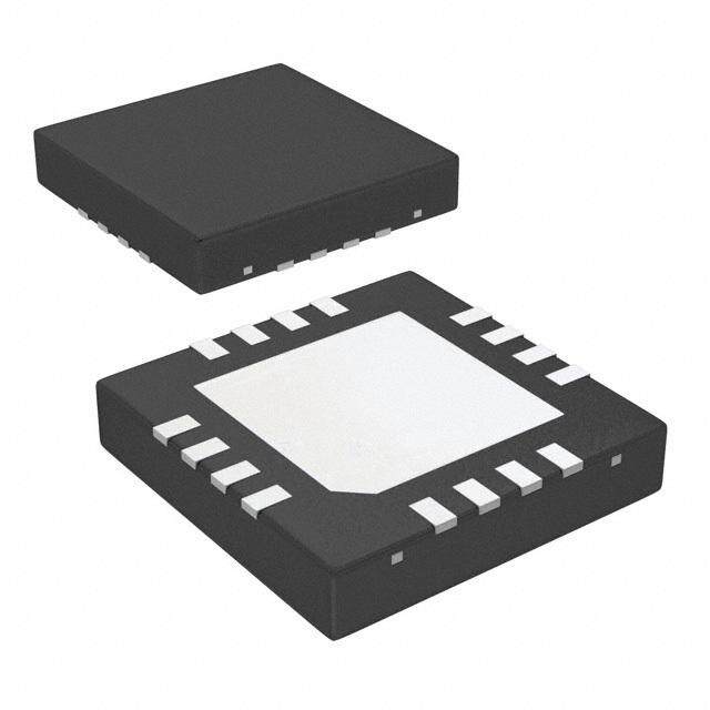
| 产品图片 |
|
| 产品型号 | LTC3562EUD#PBF |
| PWM类型 | 多重 |
| rohs | 无铅 / 符合限制有害物质指令(RoHS)规范要求 |
| 产品系列 | - |
| 供应商器件封装 | 20-QFN(3x3) |
| 包装 | 管件 |
| 同步整流器 | 是 |
| 安装类型 | 表面贴装 |
| 封装/外壳 | 20-WFQFN 裸露焊盘 |
| 工作温度 | -40°C ~ 85°C |
| 标准包装 | 121 |
| 电压-输入 | 2.85 V ~ 5.5 V |
| 电压-输出 | 425 mV ~ 800 mV,0.6 V ~ 3.78 V |
| 电流-输出 | 400mA,600mA |
| 类型 | 降压(降压) |
| 输出数 | 4 |
| 输出类型 | 可调式 |
| 频率-开关 | 2.25MHz |


PDF Datasheet 数据手册内容提取
LTC3562 2 I C Quad Synchronous Step-Down DC/DC Regulator 2 × 600mA, 2 × 400mA FEATURES DESCRIPTION n Four Independent I2C Controllable Step-Down The LTC®3562 is a quad high effi ciency monolithic syn- Regulators (2 × 600mA, 2 × 400mA) chronous step-down regulator with an I2C interface. Two n Two I2C Programmable Feedback Voltage regulators are externally adjustable and can have their Regulators (R600A, R400A): V 425mV to 800mV feedback voltages programmed between 425mV and FB n Two I2C Programmable Output Voltage Regulators 800mV in 25mV steps (Type A). The other two regulators (R600B, R400B): V 600mV to 3.775V are fi xed output regulators whose output voltages can be OUT n Programmable Modes: Pulse Skip, LDO, Burst Mode,® programmed between 600mV and 3.775V in 25mV steps Forced Burst Mode Operation (Type B). All four regulators operate independently and n Quiescent Current < 100μA (All Regulators Enabled can be put into pulse skip, LDO, Burst Mode operation, in LDO Mode) or forced Burst Mode operation through I2C control. The n Fixed 2.25MHz Switching Frequency (Pulse Skip Type-A regulators have separate RUN pins that can be Mode) enabled if I2C control is unavailable. n Slew Limiting Reduces Switching Noise The 2.85V to 5.5V input voltage range makes the LTC3562 n Power-On Reset Output for Regulator R600A ideally suited for single Li-Ion battery-powered applica- n Small, Thermally Enhanced, 20-Lead 3mm × 3mm tions. At low output load conditions, the regulators can QFN Package be switched into LDO, Burst Mode operation, or forced Burst Mode operation, extending battery life in portable APPLICATIONS systems. The quiescent current drops to under 100μA n Miscellaneous Handheld Applications with Multiple with all regulators in LDO mode, and under 0.1μA when Supply Rails all regulators are shut down. n Personal Information Appliances Switching frequency is internally set to 2.25MHz, allowing n Wireless and DSL Modems the use of small surface mount inductors and capacitors. n Digital Still Cameras All regulators are internally compensated. The LTC3562 is n MP3 Players available in a low profi le 3mm × 3mm QFN package. n Portable Instruments L, LT, LTC, LTM and Burst Mode are registered trademarks of Linear Technology Corporation. All other trademarks are the property of their respective owners. TYPICAL APPLICATION R600x Burst Mode Effi ciency High Effi ciency Quad Step-Down Converter with I2C and Power Loss vs Load Current MICROPROCESSOR 100 10000 404V010Om.05UAVALTi3-I.o4nV/ PToO1l y40m.μ2eFVr+ 10pF 4573456.kk7μ1H0μF SFRBWU4N4040000A0AVAINLTC3S5C6L2SDRPSAUOFWNRBD6666V00000000CCAAAA 100k 3.3μH V1664.0O3980U49VmTkk6A00A PSSDODCV1LCRA0CpF 10μF EFFICIENCY (%) 46789350000000 V2.O5UVTV =O VUOT U=T 3 =.3 1V.2VV1,.O8UVT = VOVUOTU =T 1=. 23V.3V 111000000POWER LOSS (mW) 20 1.8V, 2.5V 1 VOUT400B 4.7μH 3.3μH VOUT600B 10 1.2V SW400B SW600B 3.3V VIN = 3.8V 400mA 10μF OUT400BPGNDAGNDOUT600B 10μF 600mA 00.01 0.1 1 10 100 10000.1 3562 TA01 LOAD CURRENT (mA) 3562 TA01b 3562fa 1
LTC3562 ABSOLUTE MAXIMUM RATINGS PIN CONFIGURATION (Notes 1, 2) V ...............................................................–0.3V to 6V TOP VIEW IN RUN600A ......................................–0.3V to (VIN + 0.3V) 00A 00A RUN400A ......................................–0.3V to (VIN + 0.3V) SDA SCL DVCC RUN6 RUN4 FBx ...............................................................–0.3V to 6V 20 19 18 17 16 SWx .............................................................–0.3V to 6V AGND 1 15 POR600A FB400A 2 14 FB600A OUTx ............................................................–0.3V to 6V OUT400B 3 21 13 OUT600B DV , POR600A, SDA, SCL .........................–0.3V to 6V CC SW400B 4 12 SW600B ISW400x (DC) ........................................................600mA PGND 5 11 PGND I (DC) ........................................................850mA 6 7 8 9 10 SW600x A N N N A Operating Temperature (Note 2)...............–40°C to 85°C 00 VI VI VI 00 4 6 W W Storage Temperature Range ...................–65°C to 125°C S S Junction Temperature (Note 3) .............................125°C UD PACKAGE 20-LEAD (3mm × 3mm) PLASTIC QFN TJMAX = 125°C, θJA = 68°C/W EXPOSED PAD (PIN 21) IS GND, MUST BE SOLDERED TO PCB ORDER INFORMATION LEAD FREE FINISH TAPE AND REEL PART MARKING PACKAGE DESCRIPTION TEMPERATURE RANGE LTC3562EUD#PBF LTC3562EUD#TRPBF LCPV 20-Lead (3mm × 3mm) Plastic QFN –40°C to 85°C Consult LTC Marketing for parts specifi ed with wider operating temperature ranges. Consult LTC Marketing for information on non-standard lead based fi nish parts. For more information on lead free part marking, go to: http://www.linear.com/leadfree/ For more information on tape and reel specifi cations, go to: http://www.linear.com/tapeandreel/ ELECTRICAL CHARACTERISTICS The l denotes the specifi cations which apply over the full operating temperature range, otherwise specifi cations are at T = 25°C, V = 3.8V, unless otherwise noted. A IN PARAMETER CONDITIONS MIN TYP MAX UNITS V Input Voltage Range l 2.7 5.5 V IN V Input Current (Per Regulator Enabled) Pulse Skip Mode, I = 0 220 μA IN OUT Burst Mode Operation, I = 0 35 60 μA OUT Forced Burst Mode Operation, I = 0 25 40 μA OUT LDO Mode, I = 0 24 40 μA OUT Shutdown Mode, I = 0, DV = 1.8V 0.7 3 μA OUT CC V Shutdown Current All Regulators in Shutdown, DV = 0V 0.1 1 μA IN CC RUN600A, RUN400A Input High Threshold l 1.0 V RUN600A, RUN400A Input Low Threshold l 0.3 V RUN600A, RUN400A Input High Current RUNx = V –1 1 μA IN RUN600A, RUN400A Input Low Current RUNx = 0V –1 1 μA POR600A Threshold Percentage of R600A’s Final Output Voltage –8 % POR600A On-Resistance 16 40 Ω POR600A Delay 231 ms 3562fa 2
LTC3562 ELECTRICAL CHARACTERISTICS The l denotes the specifi cations which apply over the full operating temperature range, otherwise specifi cations are at T = 25°C, V = 3.8V, unless otherwise noted. A IN PARAMETER CONDITIONS MIN TYP MAX UNITS I2C Port DV Operating Voltage l 1.5 5.5 V CC DV Operating Current DV = 1.8V, Serial Port Idle 1 μA CC CC DV UVLO Threshold Voltage 1 V CC V SDA, SCL (Low Level Input Voltage) 0.3 • DV V IL CC V SDA, SCL (High Level Input Voltage) 0.7 • DV V IH CC V SDA (Digital Output Low) I = 3mA 0.08 V OL PULLUP Serial Port Timing (Note 4) t Clock Operating Frequency 400 kHz SCL t Bus Free Time Between Stop and Start Conditions 1.3 μs BUF t Hold Time After (Repeated) Start Condition 0.6 μs HD,STA t Repeated Start Condition Setup Time 0.6 μs SU,STA t Stop Condition Setup Time 0.6 μs SU,STO t Data Hold Time 225 ns HD,DAT(OUT) t Input Data Hold Time 0 900 ns HD,DAT(IN) t Data Setup Time 100 ns SU,DAT t Clock Low Period 1.3 μs LOW t Clock High Period 0.6 μs HIGH t Clock Data Fall Time 20 300 ns f t Clock Data Rise Time 20 300 ns r t Spike Suppression Time 50 ns SP BUCK DC/DC ELECTRICAL CHARACTERISTICS The l denotes the specifi cations which apply over the full operating temperature range, otherwise specifi cations are at T = 25°C, V = 3.8V, V = 1.5V, unless otherwise noted. A IN OUTx PARAMETER CONDITIONS MIN TYP MAX UNITS Regulators R600A, R400A, R600B, R400B f 1.91 2.25 2.59 MHz OSC Maximum Duty Cycle Pulse Skip Mode 100 % LDO Mode Closed Loop ROUT LDO Mode 0.25 Ω Regulators R600A, R600B PMOS Switch Current Limit Pulse Skip Mode 850 1200 1500 mA PMOS RDS(ON) 0.38 Ω NMOS RDS(ON) 0.38 Ω LDO Mode Open Loop ROUT LDO Mode 2.2 Ω Available Output Current Forced Burst Mode 75 140 mA LDO, V = 1.2V 50 mA OUT SW Pull-Down in Shutdown Shutdown 2.5 kΩ 3562fa 3
LTC3562 ELECTRICAL CHARACTERISTICS The l denotes the specifi cations which apply over the full operating temperature range, otherwise specifi cations are at T = 25°C, V = 3.8V, V = 1.5V, unless otherwise noted. A IN OUTx PARAMETER CONDITIONS MIN TYP MAX UNITS Regulators R400A, R400B PMOS Switch Current Limit Pulse Skip Mode 600 800 1000 mA PMOS RDS(ON) 0.5 Ω NMOS RDS(ON) 0.5 Ω LDO Mode Open Loop ROUT LDO Mode 3 Ω SW Pull-Down in Shutdown Shutdown 2.5 kΩ Available Output Current Forced Burst Mode 50 100 mA LDO Mode, V = 1.2V 50 mA OUT Regulators R600A, R400A V DAC = XXX1111, Pulse Skip Mode l 0.776 0.800 0.824 V FB(MAX) V DAC = XXX0000, Pulse Skip Mode l 0.412 0.425 0.438 V FB(MIN) V (0 to 15) 25 mV FB(STEP) I FB Input Current FB DAC = XXX1111 –50 0 50 nA Regulators R600B, R400B V V = 4V, DAC = 0000000, Pulse Skip Mode l 0.582 0.600 0.618 V OUT(MIN) IN V V = 4V, DAC = 1111111, l 3.661 3.775 3.889 V OUT(MAX) IN Pulse Skip Mode V (0 to 127) V = 4V 25 mV OUT(STEP) IN Note 1: Stresses beyond those listed under Absolute Maximum Ratings Note 3: This IC includes overtemperature protection that is intended may cause permanent damage to the device. Exposure to any Absolute to protect the device during momentary overload conditions. Maximum Rating condition for extended periods may affect device Overtemperature protection is active when junction temperature exceeds reliability and lifetime. the maximum operating junction temperature. Continuous operation above Note 2: The LTC3562E is guaranteed to meet performance specifi cations the specifi ed maximum operating junction temperature may result in from 0°C to 85°C. Specifi cations over the –40°C to 85°C operating device degradation or failure. temperature range are assured by design, characterization and correlation Note 4: The serial port is tested at rated operating frequency. Timing with statistical process control. parameters are tested and/or guaranteed by design. 3562fa 4
LTC3562 TYPICAL PERFORMANCE CHARACTERISTICS Effi ciency vs Load Current Effi ciency vs Load Current Effi ciency vs Load Current 100 100 100 FORCED FORCED FORCED 90 Burst Mode OPERATION 90 Burst Mode OPERATION 90 Burst Mode OPERATION 80 Burst Mode 80 80 600mA 70 OPERATION 70 600mA 70 BUCKS %) 600mA %) BUCKS %) Y ( 60 BUCKS Y ( 60 Y ( 60 NC 50 NC 50 PULSE SKIP NC 50 PULSE SKIP EFFICIE 40 PULSE SKIP EFFICIE 40 BOuPrEsRt AMToIOdeN EFFICIE 40 BOuPrEsRt AMToIOdeN 30 30 30 20 20 20 10 VIN = 3.8V 10 VIN = 3.8V 10 VIN = 3.8V VOUT = 1.2V VOUT = 1.8V VOUT = 2.5V 0 0 0 0.01 0.1 1 10 100 1000 0.01 0.1 1 10 100 1000 0.01 0.1 1 10 100 1000 IOUT (mA) IOUT (mA) IOUT (mA) 3562 G01 3562 G02 3562 G03 Effi ciency vs Input Voltage Effi ciency vs Input Voltage Effi ciency vs Load Current Burst Mode Operation Burst Mode Operation 100 100 100 FORCED Burst Mode VOUT = 1.2V VOUT = 1.8V 90 OPERATION 90 90 80 600mA 80 80 BUCKS 70 70 70 %) %) %) NCY ( 6500 Burst Mode PULSE SKIP NCY ( 6500 NCY ( 6500 EFFICIE 40 OPERATION EFFICIE 40 EFFICIE 40 30 30 IOUT = 0.1mA 30 IOUT = 0.1mA 20 20 IOUT = 1mA 20 IOUT = 1mA IOUT = 10mA IOUT = 10mA 10 VIN = 3.8V 10 IOUT = 100mA 10 IOUT = 100mA VOUT = 3.3V IOUT = 400mA IOUT = 400mA 0 0 0 0.01 0.1 1 10 100 1000 2.5 3 3.5 4 4.5 5 5.5 2.5 3 3.5 4 4.5 5 5.5 IOUT (mA) INPUT VOLTAGE (V) INPUT VOLTAGE (V) 3562 G04 3562 G05 3562 G06 Output Transient Output Transient Start-Up Transient Burst Mode Operation Pulse Skip Mode Pulse Skip Mode 5V0OmUVT4/D00IVB 5V0OmUVT4/D00IVB VOUT600A 500mV/DIV AC AC COUPLED COUPLED INDUCTOR VOUT400A VOUT600B CURRENT 50mV/DAIVC 50mV/DAIVC IL= 100mDAIV/ COUPLED COUPLED 300mA 300mA 5mA IOUT400B 5mA IOUT400B RUN600A OFF 2V/DIV ON 50μs/DIV 3562 G07 50μs/DIV 3562 G08 50μs/DIV 3562 G09 VOUT400B= 1.2V VOUT400B= 1.8V VOUT600A= 1.2V VOUT400A= 1.2V VOUT600B= 1.2V RLOAD= 6Ω IOUT400A= 20mA IOUT600B= 15mA 3562fa 5
LTC3562 TYPICAL PERFORMANCE CHARACTERISTICS R600A Feedback Voltage Oscillator Frequency Output Voltage vs Temperature vs Temperature vs Load Current (B Version) 0.810 2.5 1.220 IOUT = 1mA VIN = 3.8V 0.808 2.4 VIN = 5.5V VOUT = 1.2V (TYPE-B) VIN = 3.8V 1.215 0.806 2.3 VIN = 3V 0.804 2.2 OLTAGE (mV)000...788900820 f (MHz)OSC122...910 VIN = 2.7V VOLTAGE (V)11..221005 PULSE SKIP V 1.200 0.796 1.8 0.794 1.7 1.195 0.792 1.6 0.790 1.5 1.190 –50 –25 0 25 50 75 100 –50 –25 0 25 50 75 100 0 100 200 300 400 500 600 TEMPERATURE (°C) TEMPERATURE (°C) LOAD CURRENT (mA) 3562 G10 3562 G11 3562 G12 Dynamic Supply Current Dynamic Supply Current vs Input Voltage vs Input Voltage Burst Mode Operation 45 6 IOUT = 0mA IOUT = 0mA VOUT600A VOUT = 1.2V 50mV/DIV 40 5 N AC O COUPLED Burst Mode OPERATION A) 4 ERATI I (A)μIN 3350 CURRENT (m 32 NTINUOUS OP INCDUU2RVCR/TEDSONIWVRT FOOPRECREADTI OBuNrst Mode CO IL= 100mDAIV/ 25 1 3562 G15 2μs/DIV LDO MODE PULSE SKIP PVIN= 3.8V 20 0 OPERATION LOAD = 50mA 2.7 3.1 3.5 3.9 4.3 4.7 5.1 5.5 2 2.5 3 3.5 4 4.5 5 5.5 6 VIN VOLTAGE (V) VOLTAGE (V) 3562 G14 3562 G13 400mA – VOUT = 1.2V 400mA – VOUT = 2.5V 600mA – VOUT = 1.2V 600mA – VOUT = 2.5V 400mA – VOUT = 1.8V 400mA – VOUT = 3.3V 600mA – VOUT = 1.8V 600mA – VOUT = 3.3V Forced Burst Mode Operation Output Voltage vs Load Current Switch R vs Input Voltage DS(ON) VOUT600A 1.22 700 50mV/DIV AC 1.21 FBOuRrsCt EMDode 600 400mA PMOS COUPLED 1.20 OPERATION 400mA NMOS SW 1.19 )Ω500 600mA PMOS 2V/DIV V)1.18 (N) AGE (1.17 RDS(O400 INDUCTOR LT LDO MODE H 300 600mA NMOS CURRENT VO1.16 TC IL= 150mDAIV/ 1.15 SWI200 1.14 3562 G16 2μs/DIV 100 PLOVIAND= = 3 5.80VmA 11..1123 VVIONU =T =3 .18.V2V (TYPE-B) 0 0 20 40 60 80 100 120 140 2.7 3.1 3.5 3.9 4.3 4.7 5.1 5.5 LOAD CURRENT (mA) 3562 G17 VIN VOLTAGE (V) 3562 G18 3562fa 6
LTC3562 PIN FUNCTIONS AGND (Pin 1): Analog Ground Pin. All small-signal com- OUT600B (Pin 13): Output Voltage Feedback Pin for ponents should connect to this ground, which in turn R600B. An I2C programmable internal resistor divider connects to PGND at one point. divides the output voltage down for comparison to the internal reference voltage. This pin converges to 1 of FB400A (Pin 2): Feedback Pin for R400A. When the con- 128 possible set-points based on the programmed value trol loop is complete, this pin servos to 1 of 16 possible from the I2C serial port (see Tables 5 and 6). This node set-points based on the programmed value from the I2C must be bypassed to GND with a 10μF or greater ceramic serial port (see Table 4). capacitor. OUT400B (Pin 3): Output Voltage Feedback Pin for FB600A (Pin 14): Feedback Pin for R600A. When the con- R400B. An I2C programmable internal resistor divider trol loop is complete, this pin servos to 1 of 16 possible divides the output voltage down for comparison to the set-points based on the programmed value from the I2C internal reference voltage. This pin converges to 1 of serial port (see Table 4). 128 possible set-points based on the programmed value from the I2C serial port (see Tables 5 and 6). This node POR600A (Pin 15): Power-On Reset for R600A. This open- must be bypassed to GND with a 10μF or greater ceramic drain output goes high impedance after a 230ms delay capacitor. after the output of R600A reaches 92% of its regulation voltage. This output gets pulled to GND whenever R600A SW400B (Pin 4): Switch Node Connection to the Inductor falls below 92% of its regulation voltage. for R400B. This pin connects to the drains of the internal power MOSFET switches of R400B. RUN400A (Pin 16): Enable Pin for R400A, Active High. Apply a voltage greater than 1V to enable this regulator. PGND (Pins 5, 11): Power Ground Pin. Connect this pin closely to the (–) terminal of C . RUN600A (Pin 17): Enable Pin for R600A, Active Low. IN Apply a voltage less than 0.3V to enable this regulator. SW400A (Pin 6): Switch Node Connection to the Inductor for R400A. This pin connects to the drains of the internal DV (Pin 18): Supply Voltage for I2C Lines. This pin sets the CC power MOSFET switches of R400A. logic reference level of the LTC3562. A UVLO circuit on the DV pin forces all registers to a default setting whenever V (Pins 7, 8, 9): Input Supply Pin. This pin must be CC IN DV is < 1V. Bypass to GND with a 0.1μF capacitor. closely decoupled to GND with a 10μF or greater ceramic CC capacitor. SCL (Pin 19): I2C Clock Input. Serial data is shifted one bit per clock to control the LTC3562. The logic level for SW600A (Pin 10): Switch Node Connection to the Inductor SCL is referenced to DV . for R600A. This pin connects to the drains of the internal CC power MOSFET switches of R600A. SDA (Pin 20): I2C Data Input. The logic level for SDA is referenced to DV . SW600B (Pin 12): Switch Node Connection to the Inductor CC for R600B. This pin connects to the drains of the internal Exposed Pad (Pin 21): Ground. Must be soldered to power MOSFET switches of R600B. PCB ground for electrical contact and optimum thermal performance. 3562fa 7
LTC3562 BLOCK DIAGRAM 17 16 18 DVCC DVCC RUN600A RUN400A V7,I N8, 9 20 SDA SDA I2C EN 4 SCL 1 1 19 SCL MODE DATA R600A 2 7 4 REF600A D/A EN SW600A 0.425V-0.8V 10 REF MODE FB FB600A 14 R400A 4 REF400A D/A EN SW400A 0.425V-0.8V 6 REF MODE FB FB400A 2 R600B AGND 1 1 EN SW600B 12 0.6V REF OUT600B 13 MODE FB 7 R400B 1 EN SW400B 4 0.6V REF OUT400B 3 MODE FB POR600A 7 15 POWER GOOD 230ms Delay R600A PGND 5,11 3562 BD 3562fa 8
LTC3562 OPERATION Introduction Through I2C control, V can be programmed from FBxA 800mV (full scale) down to 425mV in 25mV increments. The LTC3562 is a highly integrated power management When the RUN pins (RUN600A and RUN400A) are used IC that contains four I2C controllable, monolithic, high ef- to activate these regulators, the default feedback servo fi ciency step-down regulators. Two regulators provide up voltage is set to 800mV. to 600mA of output current and the other two regulators produce up to 400mA. All four regulators are 2.25MHz, constant-frequency, current mode switching regulators that LTC3562 L can be independently controlled through I2C. All regula- SWxA tors are internally compensated eliminating the need for CFB R1 CO external compensation components. FBxA 425mV to 800mV R2 The LTC3562 offers two different types of adjustable GND step-down regulators. The two Type-A regulators (R600A, 3562 F01 R400A) can have the feedback voltages adjusted through I2C from 425mV to 800mV in 25mV increments. The two Figure 1. Type-A Regulator Application Circuit Type-B regulators (R600B, R400B) can have the output voltages adjusted through I2C control from 600mV to Typical values for R2 are in the range of 40k to 1MΩ. The 3.775V in 25mV increments. capacitor C cancels the pole created by the feedback FB All four converters support 100% duty cycle operation resistors and the input capacitance of the FB pin and also (low dropout mode) when their input voltage drops very helps to improve transient response for output voltages close to their output voltage. To suit a variety of applica- much greater than 0.8V. A variety of capacitor sizes can be tions, four selectable mode functions are available on used for CFB but a value of 10pF is recommended for most the LTC3562’s step-down regulators to trade-off noise applications. Experimentation with capacitor sizes between for effi ciency. 2pF and 22pF may yield improved transient response. At moderate to heavy loads, the constant-frequency pulse Regulators R600A and R400A have individual RUN pins skip mode provides the lowest output switching noise solu- that can enable the regulators without accessing the I2C tion. At lighter loads, either Burst Mode operation, forced port. The RUN600A and RUN400A pins are OR’ed with the Burst Mode operation or LDO mode may be selected to enable signals coming from the I2C port (refer to the Block optimize effi ciency. The switching regulators also include Diagram) such that regulators R600A and R400A can be soft-start to limit inrush current when powering on, short- enabled if the I2C port is unavailable. The RUN600A pin is circuit current protection, and switch node slew limiting active low and the RUN400A pin is active high. circuitry to reduce radiated EMI. No external compensation When the RUN pins are activated, the Type-A regulators components are required. are enabled in a default setting. The default mode for the regulators is pulse skip mode and the default feedback V Adjustable (Type-A) Regulators FB servo voltage setting is 800mV. Once enabled with these The two Type-A step-down regulators (R600A and R400A) default settings, the settings can always be changed on have individual programmable feedback servo voltages via the fl y through I2C once the I2C terminal is available. I2C control. Given a particular feedback servo voltage, the The maximum operating output current of regulators R600A output voltage is programmed using a resistor divider from the switching regulator output connected to the feedback and R400A are 600mA and 400mA, respectively. pins (Figure 1). The output voltage is related to the feedback servo voltage by the following equation: (cid:1)R1 (cid:4) V =V +1 OUTxA FBxA(cid:2) (cid:5) (cid:3)R2 (cid:6) 3562fa 9
LTC3562 OPERATION V Adjustable (Type-B) Regulators the peak inductor current to the output of an error amplifi er. OUT The output of the current comparator resets the internal Unlike the Type-A regulators, the two Type-B regulators latch which causes the main P-channel MOSFET switch to do not require an external resistor divider network to turn off and the N-channel MOSFET synchronous rectifi er program its output voltage. Regulators R600B and R400B to turn on. The N-channel MOSFET synchronous rectifi er have feedback resistor networks internal to the chip whose values can be adjusted through I2C control. These inter- turns off at the end of the 2.25MHz cycle or if the current through the N-channel MOSFET synchronous rectifi er nal feedback resistors can be confi gured such that the drops to zero. Using this method of operation, the error output voltages can be programmed directly. The output amplifi er adjusts the peak inductor current to deliver the voltages can be programmed from 600mV to 3.775V in required output power. All necessary compensation is 25mV increments. internal to the switching regulator requiring only a single Pins OUT600B and OUT400B are feedback sense pins that ceramic output capacitor for stability. At light loads in connect to the top of the internal resistor divider networks. pulse skip mode, the inductor current may reach zero These output pins should sense the output voltages of on each pulse which will turn off the N-channel MOSFET the regulators right at the output capacitor C (after the O synchronous rectifi er. In this case, the switch node (SW) inductor), as illustrated in Figure 2. goes high impedance and the switch node voltage will The maximum operating current for regulators R600B and “ring.” This is discontinuous mode operation, and is R400B are 600mA and 400mA, respectively. The Type-B normal behavior for a switching regulator. At very light regulators do not have individual run pins as do the Type-A loads in pulse skip mode, the switching regulators will regulators. Thus regulators R600B and R400B can only automatically skip pulses as needed to maintain output be enabled through control of the I2C port. When the regulation. At high duty cycle (V > V /2) it is possible OUT IN part initially powers up, the Type-B regulators default to for the inductor current to reverse at light loads, causing shutdown mode and remain disabled until programmed the step-down switching regulator to operate continuously. through I2C. When operating continuously, regulation and low noise output voltage are maintained, but input operating current Regulator Operating Modes will increase to a couple mA. All of the LTC3562’s switching regulators include four In forced Burst Mode operation, the switching regulators possible operating modes to meet the noise/power needs use a constant-current algorithm to control the inductor of a variety of applications. current. By controlling the inductor current directly and In pulse skip mode, an internal latch is set at the start of using a hysteretic control loop, both noise and switch- every cycle which turns on the main P-channel MOSFET ing losses are minimized. In this mode output power is switch. During each cycle, a current comparator compares limited. While operating in forced Burst Mode operation, LTC3562 L 600mV to 3.775V SWxB CO OUTxB GND 3562 F02 Figure 2. Type-B Regular Application Circuit 3562fa 10
LTC3562 OPERATION the output capacitor is charged to a voltage slightly higher Dropout Operation than the regulation point. The step-down converter then It is possible for V to approach a switching regulator’s IN goes into sleep mode, during which the output capacitor programmed output voltage (e.g., a battery voltage of 3.4V provides the load current. In sleep mode, most of the with a programmed output voltage of 3.3V). When this regulator’s circuitry is powered down, helping conserve happens, the PMOS switch duty cycle increases until it is battery power and increase effi ciency. When the output turned on continuously at 100%. In this dropout condi- voltage drops below a predetermined value, the switching tion, the respective output voltage equals the regulator’s regulator circuitry is powered on and another burst cycle input voltage minus the voltage drops across the internal begins. The duration for which the regulator operates in P-channel MOSFET and the inductor. sleep mode depends on the load current. The sleep time decreases as the load current increases. Forced Burst Mode Soft-Start Operation operation has a maximum deliverable output current of Soft-start is accomplished by gradually increasing the about 140mA for the 600mA regulators and 100mA for peak inductor current for each switching regulator over the 400mA regulators. Beyond the maximum deliverable a 500μs period. This allows each output to rise slowly, output current, the step-down switching regulator will not helping minimize the battery in-rush current. A soft- enter sleep mode and the output will drop out of regula- start cycle occurs whenever a given switching regula- tion. Forced Burst Mode operation provides a signifi cant tor is enabled, or after a fault condition has occurred improvement in effi ciency at light loads at the expense of (thermal shutdown). A soft-start cycle is not triggered higher output ripple when compared to pulse skip mode. by changing operating modes. This allows seamless For many noise-sensitive systems, forced Burst Mode output operation when transitioning between Burst operation might be undesirable at certain times (i.e., Mode operation, forced Burst Mode operation, pulse during a transmit or receive cycle of a wireless device), skip mode or LDO mode. but highly desirable at others (i.e., when the device is in low power standby mode). The I2C port can be used to Switching Slew Rate Control enable or disable forced Burst Mode operation at any time, offering both low noise and low power operation when The step-down switching regulators contain new pat- they are needed. ent pending circuitry to limit the slew rate of the switch node (SWx). This new circuitry is designed to transition In Burst Mode operation, the switching regulator automati- the switch node over a period of a couple nanoseconds, cally switches between fi xed frequency pulse skip operation signifi cantly reducing radiated EMI and conducted supply and hysteretic control as a function of the load current. At noise, while keeping effi ciency high. light loads the regulators operate in hysteretic mode and at heavy loads they operate in constant-frequency mode. Step-Down Switching Regulator in Shutdown The constant-frequency mode provides the same output ripple and effi ciency as pulse skip mode while hysteretic The step-down switching regulators are in shutdown when mode provides slightly lower output ripple than forced not enabled for operation. In shutdown, all circuitry in Burst Mode operation at the expense of slightly lower the step-down switching regulator is disconnected from effi ciency. the switching regulator input supply, leaving only a few nano-amps of leakage current. The step-down switch- Finally, the switching regulators have an LDO mode that ing regulator outputs are individually pulled to ground gives a DC option for regulating their output voltages. In through a 2k resistor on the switch pin (SWx) when in LDO mode, the switching regulators are converted to linear shutdown. regulators and deliver continuous power from their SWx pins through their respective inductors. This mode gives the lowest possible output noise as well as low quiescent current at light loads. 3562fa 11
LTC3562 OPERATION I2C Interface Acknowledge The LTC3562 may communicate with a host (master) using The Acknowledge signal is used for handshaking between the standard I2C 2-wire interface. The Timing Diagram in the master and the slave. An Acknowledge (active LOW) Figure 4 shows the timing relationship of the signals on generated by the slave (LTC3562) lets the master know the bus. The two bus lines, SDA and SCL, must be high that the latest byte of information was received. The when the bus is not in use. External pull-up resistors or Acknowledge-related clock pulse is generated by the current sources, such as the LTC1694 SMBus Accelerator, master. The master releases the SDA line (HIGH) during are required on these lines. The LTC3562 is a receive-only the Acknowledge clock cycle. The slave-receiver must pull (slave) device. The I2C control signals, SDA and SCL are down the SDA line during the Acknowledge clock pulse scaled internally to the DVCC supply. DVCC should be con- so that it remains a stable low during the high period of nected to the same power supply as the microcontroller this clock pulse. generating the I2C signals. Slave Address Byte The I2C port has an undervoltage lockout on the DV CC pin. When DV is below approximately 1V, the I2C serial The LTC3562 responds to only one 7-bit address which CC port is cleared and the two switching Type-A regulators has been factory programmed to 11001010. The eighth are set to full scale. bit of the address byte (R/W) must be 0 for the LTC3562 to recognize the address since it is a write-only device. Bus Speed This effectively forces the address to be 8 bits long where The I2C port is designed to be operated at speeds of up the least signifi cant bit of the address is 0. If the correct to 400kHz. It has built-in timing delays to ensure correct 7-bit address is given but the R/W bit is 1, the LTC3562 operation when addressed from an I2C compliant master will not respond. device. It also contains input fi lters designed to suppress glitches should the bus become corrupted. Sub-Address Byte The sub-address byte uses bits A7 through A4 to specify START and STOP Conditions the regulator(s) being programmed by that particular A bus master signals the beginning of a communication three-byte sequence (refer to Table 2). A specifi c regulator to a slave device by transmitting a start condition. A start gets programmed if its corresponding sub-address bit is condition is generated by transitioning SDA from high high, whereas the regulator ignores the 3-byte sequence to low while SCL is high. When the master has fi nished if its sub-address bit is low. Note that multiple regulators communicating with the slave, it issues a stop condition can be programmed by the same 3-byte sequence if more by transitioning SDA from low to high while SCL is high. than one of the sub-address bits are high. Bits A1 and A0 The bus is then free for communication with another I2C of the sub-address byte are used to program the operating device. mode (Table 3). Bits A3 and A2 of the sub-address byte are not used. Byte Format Data Byte Each byte sent to the LTC3562 must be 8 bits long fol- lowed by an extra clock cycle for the Acknowledge bit to The data byte only affects the regulators that are specifi ed be returned by the LTC3562. The data should be sent to to be programmed by the sub-address byte. The MSB the LTC3562 most signifi cant bit (MSB) fi rst. of the data byte (B7) is used to enable or disable the regulator(s) being programmed. A high B7 indicates an enable command, whereas a low B7 indicates a shutdown command. 3562fa 12
LTC3562 OPERATION SUB-ADDRESS DATA BYTE ADDRESS WR 1 1 0 0 1 0 1 0 A7 A6 A5 A4 A3 A2 A1 A0 B7 B6 B5 B4 B3 B2 B1 B0 START STOP SDA 1 1 0 0 1 0 1 0 ACK A7 A6 A5 A4 A3 A2 A1 A0 ACK 7 6 5 4 3 2 1 0 ACK SCL 1 2 3 4 5 6 7 8 9 1 2 3 4 5 6 7 8 9 1 2 3 4 5 6 7 8 9 3562 F03 Figure 3. Bit Assignments SDA tSU, DAT tSU, STA tBUF tLOW tHD, DAT tHD, STA tSU, STO SCL 3562 F04 tHD, STA tHIGH tSP COSNTDAIRTTION tr tf REPCEOANTDEDIT ISOTNART CONSTDOITPION COSNTDAIRTTION Figure 4. Timing Parameters Table 1. Write Word Protocol Used by the LTC3562 1 7 1 1 8 1 8 1 1 S Slave Address WR A *Sub-Address A Data Byte A P** S = Start Condition, WR = Write Bit = 0, A = Acknowledge, P = Stop Condition * The sub-address uses only the fi rst four most signifi cant bits, A7, A6, A5, and A4, for sub-addressing. The two least signifi cant bits, A1 and A0, are used to program the regulator operating mode. **Stop can be delayed until all of the data registers have been written. Table 2. Sub-Address and Data Byte Mapping SUB-ADDRESS BYTE DATA BYTE A7 A6 A5 A4 A3 A2 A1 A0 B7 B6 B5 B4 B3 B2 B1 B0 PROGRAM PROGRAM PROGRAM PROGRAM NOT USED REGULATOR ENABLE DAC CODE R600A R400A R600B R400B OPERATING REGULATOR (See Tables 4, 5 and 6) MODE (SEE TABLE 3) 3562fa 13
LTC3562 OPERATION If a Type-A regulator is being programmed, then bits B3 will ignore this stop condition and will not respond until a through B0 program the DAC that controls the regulator’s new start condition, correct address, new set of data and feedback servo voltage. This 4-bit sequence programs the stop condition are transmitted. feedback voltage from 425mV to 800mV in 25mV incre- Likewise, with only one exception, if the LTC3562 was ments (Table 4). Bits B6 through B4 are not used when previously addressed and sent valid data but not updated programming a Type-A regulator. with a Stop, it will respond to any Stop that appears on If a Type-B regulator is being programmed, then bits B6 the bus, independent of the number of Repeat-Starts that through B0 program the DAC that controls the regulator’s have occurred. If a Repeat-Start is given and the LTC3562 output voltage. This 7-bit sequence programs the output successfully acknowledges its address, it will not respond voltage from 600mV to 3.775V in 25mV increments to a Stop until all three bytes of the new data have been (Tables 5 and 6). received and acknowledged. Bus Write Operation I2C Examples The master initiates communication with the LTC3562 with To program R600A in forced Burst Mode operation with a start condition and a 7-bit address followed by the write its feedback servo voltage set to 600mV: bit R/W = 0. If the address matches that of the LTC3562, Sub-Address Byte – 1000XX10 the LTC3562 returns an Acknowledge. The master should Data Byte – 1XXX0111 then deliver the sub-address byte for the regulator(s) being programmed. Again the LTC3562 acknowledges To program R600B and R400B in LDO mode with their and then the data byte is delivered starting with the most output voltages set to 1.250V: signifi cant bit. The data byte and the two mode bits in the Sub-Address Byte – 0011XX01 sub-address byte are transferred to an internal holding Data Byte – 10011010 latch for each programmed regulator upon the return To put the entire chip in shutdown and disable all regula- of an Acknowledge. After the sub-address byte and data tors: byte have been transferred to the LTC3562, the master may terminate the communication with a stop condition. Sub-Address Byte – 1111XXXX Alternatively, a repeat-start condition can be initiated by Data Byte – 0XXXXXXX the master and the entire sequence can be repeated, this time accessing a different sub-address code to program Disabling the I2C Port another regulator. Likewise, the master can also initiate a The I2C serial port can be disabled by grounding the DV CC Repeat-Start so that another chip on the I2C bus can be pin. In this mode, regulators R600A and R400A can only be addressed. This cycle can continue indefi nitely and the activated through the individual logic input pins RUN600A LTC3562’s regulators will remember the last input of valid and RUN400A. Disabling the I2C port also resets the feed- data that it received. Once all chips on the bus have been back servo voltages to the default setting of 0.8V. addressed and sent valid data, a global stop condition can Note that if the I2C port gets disabled while a Type-A be sent and the LTC3562 will update its regulators with regulator is enabled and its RUN pin is activated, the the data that it had received. regulator will remain enabled and its feedback voltage will In certain circumstances the data on the I2C bus may immediately be reset to the default setting of 0.8V. If the become corrupted. In these cases the LTC3562 responds I2C port gets disabled and the RUN pins are not activated, appropriately by preserving only the last set of complete then the regulators will immediately go into shutdown data that it has received. For example, assume the LTC3562 mode. Since regulators R600B and R400B do not have has been successfully addressed and is receiving data RUN pins, they immediately go into shutdown once the when a stop condition mistakenly occurs. The LTC3562 I2C port gets disabled. 3562fa 14
LTC3562 OPERATION Table 3. Regulator Operating Modes Table 5. Type-B Regulator Base Output Voltage Programming A1 A0 REGULATOR MODE TYPE-B REGULATOR B6 B5 B4 B3 B2 BASE OUTPUT VOLTAGE 0 0 Pulse Skip Mode 0 0 0 0 0 0.600 0 1 LDO Mode 0 0 0 0 1 0.700 1 0 Forced Burst Mode Operation 0 0 0 1 0 0.800 1 1 Burst Mode Operation 0 0 0 1 1 0.900 0 0 1 0 0 1.000 Table 4. Type-A Regulator Servo Voltage Programming 0 0 1 0 1 1.100 TYPE-A REGULATOR B3 B2 B1 B0 SERVO (FEEDBACK) VOLTAGE 0 0 1 1 0 1.200 0 0 0 0 0.425 0 0 1 1 1 1.300 0 0 0 1 0.450 0 1 0 0 0 1.400 0 0 1 0 0.475 0 1 0 0 1 1.500 0 0 1 1 0.500 0 1 0 1 0 1.600 0 1 0 0 0.525 0 1 0 1 1 1.700 0 1 0 1 0.550 0 1 1 0 0 1.800 0 1 1 0 0.575 0 1 1 0 1 1.900 0 1 1 1 0.600 0 1 1 1 0 2.000 1 0 0 0 0.625 0 1 1 1 1 2.100 1 0 0 1 0.650 1 0 0 0 0 2.200 1 0 1 0 0.675 1 0 0 0 1 2.300 1 0 1 1 0.700 1 0 0 1 0 2.400 1 1 0 0 0.725 1 0 0 1 1 2.500 1 1 0 1 0.750 1 0 1 0 0 2.600 1 1 1 0 0.775 1 0 1 0 1 2.700 1 1 1 1 0.800 1 0 1 1 0 2.800 1 0 1 1 1 2.900 POR600A Pin 1 1 0 0 0 3.000 The POR600A pin is an open-drain output used to indicate 1 1 0 0 1 3.100 that regulator R600A has been enabled and has reached 1 1 0 1 0 3.200 its fi nal voltage. POR600A remains low impedance until 1 1 0 1 1 3.300 regulator R600A reaches 92% of its regulation value. A 1 1 1 0 0 3.400 230ms delay is included to allow a system microcontroller 1 1 1 0 1 3.500 ample time to reset itself. POR600A may be used as a 1 1 1 1 0 3.600 power on reset to the microprocessor powered by regula- 1 1 1 1 1 3.700 tor R600A or may be used to enable regulator R400A for supply sequencing. POR600A is an open drain output and Table 6. Type-B Regulator Incremental Output Voltage Programming requires a pull-up resistor to the output voltage of regulator B1 B0 TYPE-B REGULATOR INCREMENTAL OUTPUT VOLTAGE R600A or another appropriate power source. 0 0 +0.000 0 1 +0.025 1 0 +0.050 1 1 +0.075 3562fa 15
LTC3562 APPLICATIONS INFORMATION Inductor Selection Table 7 shows several inductors that work well with the LTC3562’s general purpose regulators. These inductors of- Many different sizes and shapes of inductors are avail- fer a good compromise in current rating, DCR and physical able from numerous manufacturers. Choosing the right size. Consult each manufacturer for detailed information inductor from such a large selection of devices can be on their entire selection of inductors. overwhelming, but following a few basic guidelines will make the selection process much simpler. Table 7. Recommended Inductors The step-down converters are designed to work with induc- MAX MAX SIZE INDUCTOR L I DCR (mm) tors in the range of 2.2μH to 10μH. For most applications a DC TYPE (μH) (A) (Ω) (L × W × H) MANUFACTURER 4.7μH inductor is suggested for the lower power switching DB318C 4.7 1.07 0.1 3.8 × 3.8 × 1.8 Toko regulators R400A and R400B and 3.3μH is recommended 3.3 1.20 0.07 3.8 × 3.8 × 1.8 www.toko.com for the more powerful switching regulators R600A and D312C 4.7 0.79 0.24 3.6 × 3.6 × 1.2 3.3 0.90 0.20 3.6 × 3.6 × 1.2 R600B. Larger value inductors reduce ripple current which DE2812C 4.7 1.15 0.13* 3.0 × 2.8 × 1.2 improves output ripple voltage. Lower value inductors 3.3 1.37 0.105* 3.0 × 2.8 × 1.2 DE2818C 4.7 1.25 0.072* 3.0 × 2.8 × 1.8 result in higher ripple current and improved transient re- 3.3 1.45 0.052* 3.0 × 2.8 × 1.8 sponse time, but will reduce the available output current. CDRH3D16 4.7 0.9 0.11 4 × 4 × 1.8 Sumida To maximize effi ciency, choose an inductor with a low DC 3.3 1.1 0.085 4 × 4 × 1.8 www.sumida.com resistance. For a 1.2V output, effi ciency is reduced about CDRH2D11 4.7 0.5 0.17 3.2 × 3.2 × 1.2 3.3 0.6 0.123 3.2 × 3.2 × 1.2 2% for 100mΩ series resist-ance at 400mA load current, CLS4D09 4.7 0.75 0.19 4.9 × 4.9 × 1 and about 2% for 300mΩ series resistance at 100mA load SD3118 4.7 1.3 0.162 3.1 × 3.1 × 1.8 Cooper current. Choose an inductor with a DC current rating at 3.3 1.59 0.113 3.1 × 3.1 × 1.8 www.cooperet.com least 1.5 times larger than the maximum load current to SD3112 4.7 0.8 0.246 3.1 × 3.1 × 1.2 3.3 0.97 0.165 3.1 × 3.1 × 1.2 ensure that the inductor does not saturate during normal SD12 4.7 1.29 0.117* 5.2 × 5.2 × 1.2 operation. If output short circuit is a possible condition, 3.3 1.42 0.104* 5.2 × 5.2 × 1.2 SD10 4.7 1.08 0.153* 5.2 × 5.2 × 1.0 the inductor should be rated to handle the maximum peak 3.3 1.31 0.108* 5.2 × 5.2 × 1.0 current specifi ed for the step-down converters. LPS3015 4.7 1.1 0.2 3.0 × 3.0 × 1.5 Coil Craft 3.3 1.3 0.13 3.0 × 3.0 × 1.5 www.coilcraft.com Different core materials and shapes will change the size/cur- * Typical DCR rent and price/current relationship of an inductor. Toroid or shielded pot cores in ferrite or Permalloy™ materials Input/Output Capacitor Selection are small and do not radiate much energy, but generally Low ESR (equivalent series resistance) ceramic capacitors cost more than powdered iron core inductors with similar should be used at the switching regulator outputs as well electrical characteristics. Inductors that are very thin or as the input supply. Only X5R or X7R ceramic capacitors have a very small volume typically have much higher core should be used because they retain their capacitance and DCR losses, and will not give the best effi ciency. The over wider voltage and temperature ranges than other choice of which style inductor to use often depends more ceramic types. A 10μF output capacitor is suffi cient for on the price versus size, performance, and any radiated most applications. For good transient response and sta- EMI requirements than on what the LTC3562 requires to bility the output capacitor should retain at least 4μF of operate. capacitance over operating temperature and bias voltage. The inductor value also has an effect on Burst Mode and The input supply should be bypassed with a 10μF capaci- forced Burst Mode operations. Lower inductor values will tor, or greater. Consult with capacitor manufacturers for cause the Burst Mode and forced Burst Mode switching detailed information on their selection and specifi cations frequencies to increase. of ceramic capacitors. Many manufacturers now offer 3562fa 16
LTC3562 APPLICATIONS INFORMATION very thin (<1mm tall) ceramic capacitors ideal for use in result in higher thermal resistances. height-restricted designs. Table 8 shows a list of several Furthermore, due to its high frequency switching circuitry, ceramic capacitor manufacturers. it is imperative that the input capacitors, inductors, and Table 8. Recommended Ceramic Capacitor Manufacturers output capacitors be as close to the LTC3562 as possible and that there be an unbroken ground plane under the AVX www.avxcorp.com LTC3562 and all of its external high frequency compo- Murata www.murata.com nents. High frequency currents on the LTC3562 tend to Taiyo Yuden www.t-yuden.com fi nd their way along the ground plane in a myriad of paths Vishay Siliconix www.vishay.com ranging from directly back to a mirror path beneath the TDK www.tdk.com incident path on the top of the board. If there are slits or cuts in the ground plane due to other traces on that layer, Printed Circuit Board Layout Considerations the current will be forced to go around the slits. If high To deliver maximum current under all conditions, it is critical frequency currents are not allowed to fl ow back through that the exposed metal pad on the backside of the LTC3562 their natural least-area path, excessive voltage will build package be soldered to the PC board ground. Correctly up and radiated emissions will occur. There should be a soldered to a 2500mm2 double-sided 1oz. copper board, group of vias directly under the grounded backside of the the LTC3562 has a thermal resistance of less than 68°C/W. package leading directly down to an internal ground plane. Failure to make thermal contact between the exposed pad To minimize parasitic inductance, the ground plane should on the backside of the package and the copper board will be on the second layer of the PC board. 3562 F05 Figure 5. High Frequency Ground Currents Follow Their Incident Path. Slices in the Ground Cause High Voltage and Increased Emissions. 3562fa 17
LTC3562 TYPICAL APPLICATION Quad Step-Down Converter with Push Button Control and Power Sequencing 100k Li-Ion BATTERY C5 3.4V TO 4.2V 10μF VIN SDA SCL DVCC L3 VOUT630.03BV 3.3μH SW600B LTC3562 L1 10R05k V1.O8UVT600A POR SCL SDA 600mA C3 OUT600B POR600A 3.3μH 600mA 10μF SW600A VCCCORE R1 C6 C1 L4 FB600A 634k 10pF 10μF VCCI/O VOUT400B 4.7μH RUN600A MICROPROCESSOR 1.2V SW400B R2 400mA C4 OUT400B 499k 10μF L2 VOUT400A RUN400A 4.7μH 2.5V SW400A 400mA R3 C7 C2 FB400A 1070k 10pF 10μF PGNDAGND 3562 TA02 R4 499k 3562fa 18
LTC3562 PACKAGE DESCRIPTION UD Package 20-Lead Plastic QFN (3mm × 3mm) (Reference LTC DWG # 05-08-1720 Rev Ø) 0.70 ±0.05 3.50 ± 0.05 (4 SIDES) 1.65 ± 0.05 2.10 ± 0.05 PACKAGE OUTLINE 0.20 ±0.05 0.40 BSC RECOMMENDED SOLDER PAD PITCH AND DIMENSIONS APPLY SOLDER MASK TO AREAS THAT ARE NOT SOLDERED BOTTOM VIEW—EXPOSED PAD PIN 1 NOTCH R = 0.20 TYP R = 0.115 OR 0.25 × 45° 3.00 ± 0.10 0.75 ± 0.05 TYP CHAMFER (4 SIDES) R = 0.05 19 20 TYP PIN 1 0.40 ± 0.10 TOP MARK (NOTE 6) 1 2 1.65 ± 0.10 (4-SIDES) (UD20) QFN 0306 REV A 0.200 REF 0.20 ± 0.05 0.00 – 0.05 0.40 BSC NOTE: 1. DRAWING IS NOT A JEDEC PACKAGE OUTLINE 2. DRAWING NOT TO SCALE 3. ALL DIMENSIONS ARE IN MILLIMETERS 4. DIMENSIONS OF EXPOSED PAD ON BOTTOM OF PACKAGE DO NOT INCLUDE MOLD FLASH. MOLD FLASH, IF PRESENT, SHALL NOT EXCEED 0.15mm ON ANY SIDE 5. EXPOSED PAD SHALL BE SOLDER PLATED 6. SHADED AREA IS ONLY A REFERENCE FOR PIN 1 LOCATION ON THE TOP AND BOTTOM OF PACKAGE 3562fa 19 Information furnished by Linear Technology Corporation is believed to be accurate and reliable. However, no responsibility is assumed for its use. Linear Technology Corporation makes no representa- tion that the interconnection of its circuits as described herein will not infringe on existing patent rights.
LTC3562 RELATED PARTS PART NUMBER DESCRIPTION COMMENTS LTC3406/ 600mA I , 1.5MHz, Synchronous Step-Down 96% Effi ciency, V = 2.5V, V = 5.5V, V = 0.6V, I = 20μA, OUT IN(MIN) IN(MAX) OUT(MIN) Q LTC3406B DC/DC Converter I < 1μA, ThinSOT™ Package SD LTC3407/ Dual 600mA/800mA I , 1.5MHz/2.25MHz, 95% Effi ciency, V = 2.5V, V = 5.5V, V = 0.6V, I = 40μA, OUT IN(MIN) IN(MAX) OUT(MIN) Q LTC3407-2 Synchronous Step-Down DC/DC Converter I < 1μA, MS10E and DFN Packages SD LTC3410/ 300mA I , 2.25MHz, Synchronous Step-Down 95% Effi ciency, V = 2.5V, V = 5.5V, V = 0.8V, I = 26μA, OUT IN(MIN) IN(MAX) OUT(MIN) Q LTC3410B DC/DC Converter I < 1μA, SC70 Package SD LTC3531/LTC3531-3/ 200mA I , 1.5MHz, Synchronous Buck-Boost 95% Effi ciency, V = 1.8V, V = 5.5V, V : 2V to 5V, OUT IN(MIN) IN(MAX) OUT(MIN) LTC3531-3.3 DC/DC Converter I = 16μA, I < 1μA, ThinSOT and DFN Packages Q SD LTC3532 500mA I , 2MHz, Synchronous Buck-Boost 95% Effi ciency, V = 2.4V, V = 5.5V, V : 2.4V to 5.25V, OUT IN(MIN) IN(MAX) OUT(MIN) DC/DC Converter I = 35μA, I < 1μA, MS10 and DFN Packages Q SD LTC3542 500mA I , 2.25MHz, Synchronous Step-Down 95% Effi ciency, V = 2.5V, V = 5.5V, V = 0.6V, I = 26μA, OUT IN(MIN) IN(MAX) OUT(MIN) Q DC/DC Converter ISD < 1μA, 2mm × 2mm DFN Package LTC3544/LTC3544B Quad 300mA and 2 × 200mA and 100mA, 2.25MHz, 95% Effi ciency, VIN(MIN) = 2.5V, VIN(MAX) = 5.5V, VOUT(MIN) = 0.8V, IQ = 70μA, Synchronous Step-Down DC/DC Converter ISD < 1μA, 3mm × 3mm QFN Package LTC3547/ Dual 300mA, 2.25MHz, Synchronous Step-Down 96% Effi ciency, V = 2.5V, V = 5.5V, V = 0.6V, I = 40μA, IN(MIN) IN(MAX) OUT(MIN) Q LTC3547B DC/DC Converter ISD < 1μA, 2mm × 3mm DFN Package LTC3548/LTC3548-1/ Dual 400mA and 800mA I , 2.25MHz, 95% Effi ciency, V = 2.5V, V = 5.5V, V = 0.6V, I = 40μA, OUT IN(MIN) IN(MAX) OUT(MIN) Q LTC3548-2 Synchronous Step-Down DC/DC Converter I < 1μA, MS10E and DFN Packages SD LTC3560 800mA I , 2.25MHz, Synchronous Step-Down 95% Effi ciency, V = 2.5V, V = 5.5V, V = 0.6V, I = 16μA, OUT IN(MIN) IN(MAX) OUT(MIN) Q DC/DC Converter I < 1μA, ThinSOT Package SD ThinSOT is a trademark of Linear Technology Corporation 3562fa 20 Linear Technology Corporation LT 1207 REV A • PRINTED IN USA 1630 McCarthy Blvd., Milpitas, CA 95035-7417 (408) 432-1900 ● FAX: (408) 434-0507 ● www.linear.com © LINEAR TECHNOLOGY CORPORATION 2007