ICGOO在线商城 > 集成电路(IC) > 接口 - 驱动器,接收器,收发器 > LTC2872IUHF#PBF

 Datasheet下载
- 型号: LTC2872IUHF#PBF
- 制造商: LINEAR TECHNOLOGY
- 库位|库存: xxxx|xxxx
- 要求:
| 数量阶梯 | 香港交货 | 国内含税 |
| +xxxx | $xxxx | ¥xxxx |
查看当月历史价格
查看今年历史价格
LTC2872IUHF#PBF产品简介:
ICGOO电子元器件商城为您提供LTC2872IUHF#PBF由LINEAR TECHNOLOGY设计生产,在icgoo商城现货销售,并且可以通过原厂、代理商等渠道进行代购。 LTC2872IUHF#PBF价格参考。LINEAR TECHNOLOGYLTC2872IUHF#PBF封装/规格:接口 - 驱动器,接收器,收发器, 4/4 Transceiver Full Multiprotocol 38-QFN (5x7)。您可以下载LTC2872IUHF#PBF参考资料、Datasheet数据手册功能说明书,资料中有LTC2872IUHF#PBF 详细功能的应用电路图电压和使用方法及教程。
LTC2872IUHF#PBF是Linear Technology(现隶属于Analog Devices)推出的一款高性能RS-485/RS-422收发器,广泛应用于工业自动化、通信系统及嵌入式设备中。该器件支持半双工或全双工通信模式,具备高抗噪能力和宽温工作范围(工业级温度:-40°C 至 +125°C),适用于严苛的工业环境。

典型应用场景包括工业控制总线通信,如PLC(可编程逻辑控制器)、DCS(分布式控制系统)和现场仪表之间的数据传输;也可用于远程传感器接口、楼宇自动化系统(如HVAC控制)、电力监控设备及智能电表等需要可靠长距离通信的场合。其集成故障保护功能(无需外部保护元件即可承受±40V共模电压)提高了系统可靠性,降低了设计复杂度。

此外,LTC2872IUHF#PBF具有低功耗待机模式,适合对能效有要求的应用,如电池供电或远程终端设备。其小封装(16引脚耐热增强型TSSOP)节省PCB空间,便于在紧凑型设备中集成。整体而言,该收发器适用于要求高稳定性、强抗干扰能力和长距离串行通信的工业与通信领域。
| 参数 | 数值 |
| 产品目录 | 集成电路 (IC) |
| 描述 | IC TXRX RS232/485/422 MULTIPRTCL |
| 产品分类 | |
| 品牌 | Linear Technology |
| 数据手册 | |
| 产品图片 |
|
| 产品型号 | LTC2872IUHF#PBF |
| rohs | 无铅 / 符合限制有害物质指令(RoHS)规范要求 |
| 产品系列 | - |
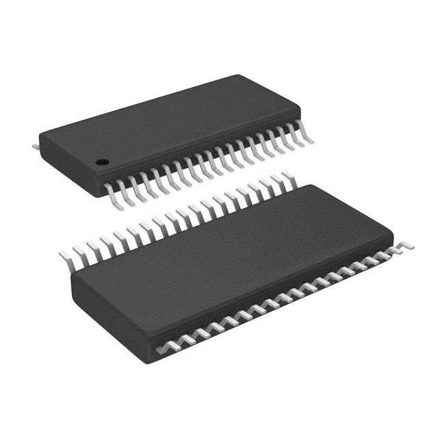
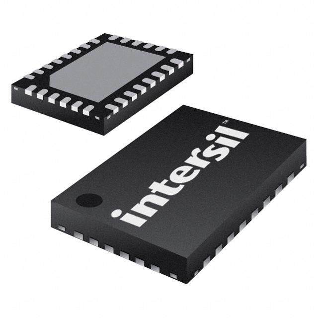
| 供应商器件封装 | 38-QFN(5x7) |
| 其它名称 | LTC2872IUHFPBF |
| 包装 | 管件 |
| 协议 | 多协议 |
| 双工 | 全 |
| 安装类型 | 表面贴装 |
| 封装/外壳 | 38-WFQFN 裸露焊盘 |
| 工作温度 | -40°C ~ 85°C |
| 接收器滞后 | 190mV |
| 数据速率 | 20Mbps |
| 标准包装 | 52 |
| 电压-电源 | 3 V ~ 5.5 V |
| 类型 | 收发器 |
| 配用 | /product-detail/zh/DC1851A/DC1851A-ND/3770246 |
| 驱动器/接收器数 | 4/4 |


- 商务部:美国ITC正式对集成电路等产品启动337调查
- 曝三星4nm工艺存在良率问题 高通将骁龙8 Gen1或转产台积电
- 太阳诱电将投资9.5亿元在常州建新厂生产MLCC 预计2023年完工
- 英特尔发布欧洲新工厂建设计划 深化IDM 2.0 战略
- 台积电先进制程称霸业界 有大客户加持明年业绩稳了
- 达到5530亿美元!SIA预计今年全球半导体销售额将创下新高
- 英特尔拟将自动驾驶子公司Mobileye上市 估值或超500亿美元
- 三星加码芯片和SET,合并消费电子和移动部门,撤换高东真等 CEO
- 三星电子宣布重大人事变动 还合并消费电子和移动部门
- 海关总署:前11个月进口集成电路产品价值2.52万亿元 增长14.8%


PDF Datasheet 数据手册内容提取
LTC2872 RS232/RS485 Dual Multiprotocol Transceiver with Integrated Termination FeaTures DescripTion n Four RS232 and Two RS485 Transceivers The LTC®2872 is a robust pin-configurable transceiver n 3V to 5.5V Supply Voltage that supports RS232, RS485, and RS422 standards while n 20Mbps RS485 and 500kbps RS232 operating on a single 3V to 5.5V supply. The LTC2872 can n Automatic Selection of Integrated RS485 (120Ω) be configured as four RS232 single-ended transceivers and RS232 (5kΩ) Termination Resistors or two RS485 differential transceivers, or combinations n Half-/Full-Duplex RS485 Switching of both, on shared I/O lines. n Logic Loopback Mode Pin-controlled integrated termination resistors allow n High ESD: ±16kV on Line I/O for easy interface reconfiguration, eliminating external n 1.7V to 5.5V Logic Interface resistors and control relays. Half-duplex switches allow n Supports Up to 256 RS485 Nodes four-wire and two-wire RS485 configurations. Loopback n RS485 Receiver Full Failsafe Eliminates UART Lockup mode steers the driver inputs to the receiver outputs for n Available in 38-Pin 5mm × 7mm QFN Package diagnostic self-test. The RS485 receivers support up to applicaTions 256 nodes per bus, and feature full failsafe operation for floating, shorted or terminated inputs. n Flexible RS232/RS485/RS422 Interface n Software Selectable Multiprotocol Interface Ports An integrated DC/DC boost converter uses a small induc- n Point-of-Sale Terminals tor and one capacitor, eliminating the need for multiple n Cable Repeaters supplies for driving RS232 levels. n Protocol Translators L, LT, LTC, LTM, Linear Technology, the Linear logo and µModule are registered trademarks of n PROFIBUS-DP Networks Linear Technology Corporation. All other trademarks are the property of their respective owners. Typical applicaTions RS485 Mode with Duplex Control RS232 Mode Mixed Mode with RS485 Termination 1.7V TO VCC 3V TO 5.5V 1.7V TO VCC 3V TO 5.5V 1.7V TO VCC 3V TO 5.5V 470nF 22µH 470nF 22µH 470nF 22µH 2.2µF 2.2µF 2.2µF 2.2µF 2.2µF 2.2µF VLCAP SW VCC VLCAP SW VCC VLCAP SW VCC FULRLS4H8A5LF H/F LTC2872 Y1 DY1 LTC2872 Y1 OFRFS4O8N5 TE485-1 LTC2872 Y1 DUPLEX DY1 TERMINATION 120Ω Z1 DY1 DZ1 Z1 Z1 RA1 A1 A1 A1 RA1 120Ω RA1 B1 B1 RB1 B1 Y2 DY2 Y2 DY2 Y2 DY2 Z2 DZ2 Z2 DZ2 Z2 RA2 A2 RA2 A2 A2 RA2 B2 RB2 B2 RB2 B2 VDD VEE VDD VEE VDD VEE 2.2µF 2.2µF 2.2µF 2.2µF 2.2µF 2.2µF 2872 TA01 2872f 1
LTC2872 absoluTe MaxiMuM raTings pin conFiguraTion (Note 1) Input Supplies TOP VIEW V , V .....................................................–0.3V to 7V 1 1 D 2 2 CC L RB RA LB VL GN RA RB Generated Supplies 38 37 36 35 34 33 32 VDD ................................................VCC – 0.3V to 7.5V VCC 1 31 VCC V .........................................................0.3V to –7.5V A1 2 30 A2 EE V – V ..............................................................15V B1 3 29 B2 DD EE Y1 4 28 Y2 SW ...........................................–0.3V to (V + 0.3V) DD GND 5 27 GND CAP .............................................0.3V to (V – 0.3V) EE Z1 6 26 Z2 A1, A2, B1, B2, Y1, Y2, Z1, Z2 ......................–15V to 15V 39 DY1 7 VEE 25 DY2 DY1, DY2, DZ1, DZ2, RXEN1, RXEN2, DXEN1, DXEN2, DZ1 8 24 DZ2 LB, H/F, TE485_1, TE485_2, RXEN1 9 23 RXEN2 485/232_1, 485/232_2 ................................–0.3V to 7V DXEN1 10 22 DXEN2 FEN, RA1, RA2, RB1, RB2 ...............–0.3V to (V + 0.3V) TE485_1 11 21 VCC L Differential Enabled Terminator Voltage TE485_2 12 20 VDD 13 14 15 16 17 18 19 (A1-B1 or A2-B2 or Y1-Z1 or Y2-Z2) .....................±6V 1 2 F N P D W Operating Temperature 32_ 32_ H/ FE CA GN S 2 2 5/ 5/ LTC2872C ................................................0°C to 70°C 8 8 4 4 LTC2872I .............................................–40°C to 85°C UHF PACKAGE 38-LEAD (5mm × 7mm) PLASTIC QFN Storage Temperature Range ..................–65°C to 125°C TJMAX = 125°C, θJA = 34.7°C/W EXPOSED PAD (PIN #39) IS VEE, MUST BE SOLDERED TO PCB orDer inForMaTion LEAD FREE FINISH TAPE AND REEL PART MARKING* PACKAGE DESCRIPTION TEMPERATURE RANGE LTC2872CUHF#PBF LTC2872CUHF#TRPBF 2872 38-Lead (5mm × 7mm) Plastic QFN 0°C to 70°C LTC2872IUHF#PBF LTC2872IUHF#TRPBF 2872 38-Lead (5mm × 7mm) Plastic QFN –40°C to 85°C Consult LTC Marketing for parts specified with wider operating temperature ranges. *The temperature grade is identified by a label on the shipping container. Consult LTC Marketing for information on non-standard lead based finish parts. For more information on lead free part marking, go to: http://www.linear.com/leadfree/ For more information on tape and reel specifications, go to: http://www.linear.com/tapeandreel/ 2872f 2
LTC2872 elecTrical characTerisTics The l denotes the specifications which apply over the full operating temperature range, otherwise specifications are at T = 25°C. V = V = 3.3V, TE485_1 = TE485_2 = 0V, LB = 0V unless otherwise noted. A CC L SYMBOL PARAMETER CONDITIONS MIN TYP MAX UNITS Power Supply V Supply Voltage Operating Range l 3 5.5 V CC V Logic Supply Voltage Operating Range V ≤ V l 1.7 V V L L CC CC V Supply Current in Shutdown Mode RXEN1 = RXEN2 = V , l 8 60 µA CC L DXEN1 = DXEN2 = FEN = H/F = 0V V Supply Current in RS485 Transceiver Mode 485/232_1 = 485/232_2 = DXEN1 = l 4.5 7 mA CC (Outputs Unloaded) (Note 3) DXEN2 = V , RXEN1 = RXEN2 = 0V L V Supply Current in RS232 Transceiver Mode DXEN1 = DXEN2 = V ; 485/232_1 = l 5.5 8 mA CC L (Outputs Unloaded) (Note 3) 485/232_2 = RXEN1 = RXEN2 = 0V V Supply Current in RS485 or RS232 Transceive DXEN1 = DXEN2 = V , RXEN1 = RXEN2 = 0V l 0 5 µA L L Mode (Outputs Unloaded) RS485 Drivers |V | Differential Output Voltage R = ∞, V = 3V (Figure 1) l 6 V OD L CC R = 27Ω, V = 4.5V (Figure 1) l 2.1 V V L CC CC R = 27Ω, V = 3V (Figure 1) l 1.5 V V L CC CC R = 50Ω, V = 3.13V (Figure 1) l 2 V V L CC CC ∆|V | Difference in Magnitude of Differential Output R = 27Ω, V = 3V (Figure 1) l 0.2 V OD L CC Voltage for Complementary Output States R = 50Ω, V = 3.13V (Figure 1) l 0.2 V L CC V Common Mode Output Voltage R = 27Ω or 50Ω (Figure 1) l 3 V OC L ∆|V | Difference in Magnitude of Common Mode R = 27Ω or 50Ω (Figure 1) l 0.2 V OC L Output Voltage for Complementary Output States I Three-State (High Impedance) Output Current V = 12V or –7V, l –100 125 µA OZD485 OUT V = 0V or 3.3V (Figure 2) CC I Maximum Short-Circuit Current –7V ≤ V ≤ 12V (Figure 2) l –250 250 mA OSD485 OUT RS485 Receiver I Input Current V = 12V or –7V, V = 0V or 3.3V l –100 125 µA IN485 IN CC (Figure 3) (Note 5) R Input Resistance V = 12V or –7V, V = 0V or 3.3V 125 kΩ IN485 IN CC (Figure 3) (Note 5) Differential Input Signal Threshold Voltage (A–B) –7V ≤ (A or B) ≤ 12 (Note 5) l ±200 mV Differential Input Signal Hysteresis B = 0V (Notes 3, 5) 190 mV Differential Input DC Failsafe Threshold Voltage –7V ≤ (A or B) ≤ 12 (Note 5) l –200 –65 0 mV (A–B) Differential Input DC Failsafe Hysteresis B = 0V (Note 5) 30 mV V Output Low Voltage Output Low, I(RA) = 3mA (Sinking), l 0.4 V OL 3V ≤ V ≤ 5.5V L Output Low, I(RA) = 1mA (Sinking), l 0.4 V 1.7V ≤ V < 3V L V Output High Voltage Output High, I(RA) = –3mA (Sourcing), l V – 0.4 V OH L 3V ≤ V ≤ 5.5V L Output High, I(RA) = –1mA (Sourcing), l V – 0.4 V L 1.7V ≤ V < 3V L Three-State (High Impedance) Output Current 0V ≤ RA ≤ V , V = 5.5V l 0 ±5 μA L L Short-Circuit Output Current 0V ≤ RA ≤ V , V = 5.5V l ±135 mA L L R Terminating Resistor TE485 = V , A–B = 2V, B = –7V, 0V, 10V l 108 120 156 Ω TERM L (Figure 8) (Note 5) 2872f 3
LTC2872 elecTrical characTerisTics The l denotes the specifications which apply over the full operating temperature range, otherwise specifications are at T = 25°C. V = V = 3.3V, TE485_1 = TE485_2 = 0V, LB = 0V unless otherwise noted. A CC L SYMBOL PARAMETER CONDITIONS MIN TYP MAX UNITS RS232 Driver V Output Low Voltage R = 3kΩ, V ≤ –6V l –5 –5.7 V V OLD L EE EE V Output High Voltage R = 3kΩ, V ≥ 6.5V l 5 6.2 V V OHD L DD DD Three-State (High Impedance) Output Current Y or Z = ±15V l ±156 µA Output Short-Circuit Current Y or Z = 0V l ±35 ±90 mA RS232 Receiver Input Threshold Voltage l 0.6 1.5 2.5 V Input Hysteresis l 0.1 0.4 1.0 V Output Low Voltage I(RA, RB) = 1mA (Sinking), l 0.4 V 1.7V ≤ V ≤ 5.5V L Output High Voltage I(RA, RB) = –1mA (Sourcing), l V – 0.4 V L 1.7V ≤ V ≤ 5.5V L Input Resistance –15V ≤ (A, B) ≤ 15V, Receiver Enabled l 3 5 7 kΩ Three-State (High Impedance) Output Current 0V ≤ (RA, RB) ≤ V l 0 ±5 μA L Output Short-Circuit Current V = 5.5V, 0V ≤ (RA, RB) ≤ V l ±25 ±50 mA L L Logic Inputs Threshold Voltage l 0.4 0.75•V V L Input Current l 0 ±5 µA Power Supply Generator V Regulated V Output Voltage RS232 Drivers Enabled, Outputs Loaded with 7 V DD DD R = 3kΩ to GND, DY1 = DY2 = V , V Regulated V Output Voltage L L –6.3 V EE EE DZ1 = DZ2 = 0V (Note 3) ESD Interface Pins (A, B, Y, Z) Human Body Model to GND or V , Powered ±16 kV CC or Unpowered (Note 7) All Other Pins Human Body Model (Note 7) ±4 kV 2872f 4
LTC2872 swiTching characTerisTics The l denotes the specifications which apply over the full operating temperature range, otherwise specifications are at T = 25°C. V = V = 3.3V, TE485_1 = TE485_2 = 0V, LB = 0V unless otherwise A CC L noted. V ≤ V . L CC SYMBOL PARAMETER CONDITIONS MIN TYP MAX UNITS RS485 AC Characteristics Maximum Data Rate (Note 3) l 20 Mbps t Driver Propagation Delay R = 54Ω, C = 100pF (Figure 4) l 20 70 ns PLHD485 DIFF L t PHLD485 Driver Propagation Delay Difference R = 54Ω, C = 100pF (Figure 4) l 1 6 ns DIFF L |t – t | PLHD485 PHLD485 t Driver Skew (Y to Z) R = 54Ω, C = 100pF (Figure 4) l 1.5 ±8 ns SKEWD485 DIFF L t , t Driver Rise or Fall Time R = 54Ω, C = 100pF (Figure 4) l 7.6 15 ns RD485 FD485 DIFF L t , t , Driver Output Enable or Disable Time FEN = V , R = 500Ω, C = 50pF (Figure 5) l 120 ns ZLD485 ZHD485 L L L t , t LZD485 HZD485 t , t Driver Enable from Shutdown FEN = 0V, R = 500Ω, C = 50pF (Figure 5) l 0.2 2 ms ZHSD485 ZLSD485 L L t , t Receiver Input to Output C = 15pF, V = 1.5V, |A–B| = 1.5V, (Figure 6) l 55 85 ns PLHR485 PHLR485 L CM (Note 5) t Differential Receiver Skew C = 15pF (Figure 6) l 1 9 ns SKEWR485 L |t – t | PLHR485 PHLR485 t , t Receiver Output Rise or Fall Time C = 15pF (Figure 6) l 3 15 ns RR485 FR485 L t , t Receiver Output Enable or Disable Time FEN = V , R = 1k, C = 15pF (Figure 7) l 30 85 ns ZLR485 ZHR485 L L L t , t LZR485 HZR485 t , t Termination Enable or Disable Time FEN = V , V = 0V, V = 2V (Figure 8) (Note 5) l 100 µs RTEN485 RTZ485 L B AB RS232 AC Characteristics Maximum Data Rate R = 3kΩ, C = 2500pF, l 100 kbps L L R = 3kΩ, C = 500pF (Note 3) l 500 kbps L L Driver Slew Rate (Figure 9) R = 3kΩ, C = 2500pF l 4 V/µs L L R = 3kΩ, C = 50pF l 30 V/µs L L t , t Driver Propagation Delay R = 3kΩ, C = 50pF (Figure 9) l 1 2 µs PHLD232 PLHD232 L L t Driver Skew R = 3kΩ, C = 50pF (Figure 9) 50 ns SKEWD232 L L t , t Driver Output Enable or Disable Time FEN = V , R = 3kΩ, C = 50pF (Figure 10) l 0.4 2 µs ZLD232 ZHD232 L L L t , t LZD232 HZD232 t , t Receiver Propagation Delay C = 150pF (Figure 11) l 60 200 ns PHLR232 PLHR232 L t Receiver Skew C = 150pF (Figure 11) 25 ns SKEWR232 L t , t Receiver Rise or Fall Time C = 150pF (Figure 11) l 60 200 ns RR232 FR232 L t , t , Receiver Output Enable or Disable Time FEN = V , R = 1kΩ, C = 150pF (Figure 12) l 0.7 2 µs ZLR232 ZHR232 L L L t , t LZR232 HZR232 Power Supply Generator VDD/VEE Supply Rise Time FEN = , (Notes 3 and 4) l 0.2 2 ms Note 1: Stresses beyond those listed under Absolute Maximum Ratings Note 4. Time from FEN until V ≥ 5V and V ≤ –5V. External DD EE may cause permanent damage to the device. Exposure to any Absolute components as shown in typical application. Maximum Rating condition for extended periods may affect device Note 5. Condition applies to A, B for H/F = 0V, and Y, Z for H/F = V . L reliability and lifetime. Note 6. This IC includes overtemperature protection that is intended Note 2. All currents into device pins are positive; all currents out of device to protect the device during momentary overload conditions. pins are negative. All voltages are referenced to device ground unless Overtemperature protection activates at a junction temperature exceeding otherwise specified. 150°C. Continuous operation above the specified maximum operating Note 3. Guaranteed by other measured parameters and not tested directly. junction temperature may result in device degradation or failure. Note 7. Guaranteed by design and not subject to production test. 2872f 5
LTC2872 Typical perForMance characTerisTics V Supply Current vs Supply V Supply Current vs Supply V Supply Current CC CC CC Voltage in Shutdown Mode Voltage in Fast Enable Mode vs RS485 Data Rate 30 4.6 200 ALL RS485 DRIVERS AND VCC = 5V 4.4 180 RECEIVERS SWITCHING. VCC = 3.3V 25 Y TIED TO A; Z TIED TO B, 160 NET (µA) 20 H/F HIGH ENT (mA)44..20 2855°°CC ENT (mA)114200 OHN/F Y= A0VN,D C LZ =T O1 0G0NpDF E R R DRIVER AND RECEIVER R 15 R3.8 R100 R U U TERMINATION ENABLED INPUT CU 10 H/F LOW SUPPLY C33..46 –40°C SUPPLY C 6800 40 5 TERMINATION DISABLED 3.2 20 0 3.0 0 3 3.5 4 4.5 5 5.5 3 3.5 4 4.5 5 5.5 0.1 1 10 100 INPUT VOLTAGE (V) SUPPLY VOLTAGE (V) DATA RATE (Mbps) 2872 G01 2872 G02 2872 G03 V Supply Current CC V Supply Current vs Supply Voltage for RS485 RS485 Driver Differential Output CC vs RS232 Data Rate at Maximum Data Rate Voltage vs Temperature 50 240 4.5 45 AALNLD RRSE2C3E2I VDERRISV ERS VVCCCC == 53V.3V 220 BROECTHEI VRESR4S8 5S DWRITIVCEHRINSG A.ND 4.0 RL = 100Ω SWITCHING Y TIED TO A, Z TIED TO B H/F = 0V 3.5 T CURRENT (mA) 32435500 2.5nF 0.05nF 0.5nF LY CURRENT (mA)112184060000 YDT2E0 RARMINVMbDEpIR NsZ ,A A TCTNOLIOD G=N R N1 EED0NC0EApIBFV LOEERND VOLTAGE (V)232...500 RRLL == 15040ΩΩ RL = 54Ω PU PP 1.5 IN 20 2.5nF 0.5nF SU120 1.0 85°C 15 0.05nF 100 25°C 0.5 VCC = 5V –40°C VCC = 3.3V 10 80 0 0 50 100150200250300350400450500 3 3.5 4 4.5 5 5.5 –50 –25 0 25 50 75 100 DATA RATE (kbps) SUPPLY VOLTAGE (V) TEMPERATURE (°C) 2872 G04 2872 G05 2872 G06 RS485 Driver Propagation Delay RS485 Driver Short-Circuit Current RS485 Driver and Receiver Skew vs Temperature vs Short-Circuit Voltage vs Temperature 50 150 3.0 VCC = 3.3V, VL = 1.7V VCC = 5V VCC = 5V, VL = 1.7V VCC = 3.3V 40 VCC = 3.3V, VL = 3.3V A) 100 2.5 VCC = 5V, VL = 5V T (m EN 50 OUTPUT LOW 2.0 AY (ns) 30 T CURR 0 W (ns)1.5 DRIVER DEL 20 RCUI SKE CI –50 1.0 ORT- OUTPUT HIGH RECEIVER 10 H S–100 0.5 0 –150 0 –50 –25 0 25 50 75 100 –10 –5 0 5 10 15 –50 –25 0 25 50 75 100 TEMPERATURE (°C) SHORT-CIRCUIT VOLTAGE (V) TEMPERATURE (°C) 2872 G07 2872 G08 2872 G09 2872f 6
LTC2872 Typical perForMance characTerisTics RS485 Receiver Propagation RS485 Receiver Output Voltage RS232 Receiver Input Threshold Delay vs Temperature vs Load Current vs Temperature 80 6 2.0 VCC = 3.3V, VL = 1.7V VL = 5V VCC = 5V, VL = 1.7V VL = 3.3V VCC = 3.3V, VL = 3.3V 5 VL = 1.7V 1.8 AY (ns) 7600 VCC = 5V, VL = 5V VOLTAGE (V) 43 D VOLTAGE (V)1.6 INPUT HIGH DEL 50 OUTPUT 2 THRESHOL1.4 INPUT LOW 1.2 1 VCC = 5V VCC = 3.3V 40 0 1.0 –50 –25 0 25 50 75 100 0 2 4 6 8 10 –50 –25 0 25 50 75 100 TEMPERATURE (°C) OUTPUT CURRENT (mA) TEMPERATURE (°C) 2872 G10 2872 G11 2872 G12 RS232 Receiver Output Voltage RS485 Termination Resistance vs Load Current vs Temperature RS232 Operation at 500kbps 6 130 VL = 5V VCM = –7V DY VL = 3.3V 128 VCM = 2V 5 VL = 1.7V 126 VCM = 12V DZ V) 124 E ( 4 Ω) Z AG E (122 5V/DIV T VOLT 3 STANC120 Y OUTPU 2 RESI111186 RRAB 114 1 1µs/DIV 2872 G15 112 WRAPPING DATA DOUT LOADS: 5kΩ + 50pF 0 110 0 2 4 6 8 10 –50 –25 0 25 50 75 100 OUTPUT CURRENT (mA) TEMPERATURE (°C) 2872 G13 2872 G14 RS232 Driver Outputs Enabling RS485 Operation at 20Mbps and Disabling V and V Powering Up DD EE 5V/DIV DY DXEN 2V/DIV FEN Y Z FEN = VL 1V/DIV 5V/DIV Z Y VDD Y 5V/DIV 5V/DIV RA Z FEN = 0V VEE 20ns/DIV 2872 G16 40ns/DIV 2872 G17 100µs/DIV 2872 G18 H/F HIGH Y, Z LOADS: 120Ω (DIFF) + 50pF 2872f 7
LTC2872 pin FuncTions V (Pins 1, 21, 31): Input Supply (3.0V to 5.5V). Tie all DY2 (Pin 25): RS485 Differential Driver #2 Input or RS232 CC three pins together and connect 2.2µF capacitor between Driver #2y Input. VCC and GND. DZ1 (Pin 8): RS232 Driver #1z Input. V (Pin 35): Logic Supply (1.7V to 5.5V) for the receiver L DZ2 (Pin 24): RS232 Driver #2z Input. outputs, driver inputs, and control inputs. This pin should be bypassed to GND with a 0.1µF capacitor if it is not tied Y1 (Pin 4): RS485 Differential Driver #1 Positive Output to V . V must be less than or equal to V for proper or RS232 Driver #1y Output, RS485 Differential Receiver CC L CC operation. #1 Positive Input (Half-Duplex Mode). V (Pin 20): Generated Positive Supply Voltage for RS232 Y2 (Pin 28): RS485 Differential Driver #2 Positive Output DD Driver (7V). Connect 2.2µF capacitor between V and GND. or RS232 Driver #2y Output, RS485 Differential Receiver DD #2 Positive Input (Half-Duplex Mode). V (Pin 39):Generated Negative Supply Voltage for RS232 EE Driver (–6.3V). Tie all pins together and connect 2.2µF Z1 (Pin 6): RS485 Differential Driver #1 Negative Output capacitor between V and GND. or RS232 Driver #1z Output, RS485 Differential Receiver EE #1 Negative Input (Half-Duplex Mode). GND (Pins 5, 18, 27, 34): Ground. Tie all four pins together. Z2 (Pin 26): RS485 Differential Driver #2 Negative Output CAP (Pin 17): Charge Pump Capacitor for Generated Nega- or RS232 Driver #2z Output, RS485 Differential Receiver tive Supply Voltage. Connect a 470nF capacitor between #2 Negative Input (Half-Duplex Mode). CAP and SW. 485/232_1 (Pin 13): Interface Select #1 Input. A logic low SW (Pin 19): Switch Pin. Connect 22µH inductor between enables RS232 mode and a high enables RS485 mode for SW and V . CC transceiver #1. The mode determines which transceiver A1 (Pin 2): RS485 Differential Receiver #1 Positive Input inputs and outputs are accessible at the LTC2872 pins (Full-Duplex Mode) or RS232 Receiver #1a Input. as well as which is controlled by the driver and receiver enable pins. A2 (Pin 30): RS485 Differential Receiver #2 Positive Input (Full-Duplex Mode) or RS232 Receiver #2a Input. 485/232_2 (Pin 14): Interface Select #2 Input. A logic low enables RS232 mode and a high enables RS485 mode for B1 (PIn 3): RS485 Differential Receiver #1 Negative Input transceiver #2. The mode determines which transceiver (Full-Duplex Mode) or RS232 Receiver #1b Input. inputs and outputs are accessible at the LTC2872 pins B2 (Pin 29): RS485 Differential Receiver #1 Negative Input as well as which is controlled by the driver and receiver (Full-Duplex Mode) or RS232 Receiver #2b Input. enable pins. RA1 (Pin 37): RS485 Differential Receiver #1 Output or RXEN1 (Pin 9): Receivers #1 Enable. A logic high disables RS232 Receiver #1a Output. RS232 and RS485 receivers in transceiver #1, leaving their outputs Hi-Z. A logic low enables the RS232 or RS485 RA2 (Pin 33): RS485 Differential Receiver #2 Output or receivers in transceiver #1, depending on the state of the RS232 Receiver #2a Output. Interface Select Input 485/232_1. RB1 (Pin 38): RS232 Receiver #1b Output. RXEN2 (Pin 23): Receivers #2 Enable. A logic high disables RB2 (Pin 32): RS232 Receiver #2b Output. RS232 and RS485 receivers in transceiver #2, leaving their DY1 (Pin 7): RS485 Differential Driver #1 Input or RS232 outputs Hi-Z. A logic low enables the RS232 or RS485 Driver #1y Input. receivers in transceiver #2, depending on the state of the Interface Select Input 485/232_2. 2872f 8
LTC2872 pin FuncTions DXEN1 (Pin 10): Drivers #1 Enable. A logic low disables the H/F (Pin 15): RS485 Half-duplex Select Input for Trans- RS232 and RS485 drivers in transceiver #1, leaving their ceivers #1 and #2. A logic low is used for full duplex outputs in a Hi-Z state. A logic high enables the RS232 or operation where pins A and B are the receiver inputs and RS485 drivers in transceiver #1, depending on the state pins Y and Z are the driver outputs. A logic high is used of the Interface Select Input 485/232_1. for half duplex operation where pins Y and Z are both the receiver inputs and driver outputs and pins A and B do DXEN2 (Pin 22): Drivers #2 Enable. A logic low disables the not serve as the receiver inputs. The impedance on A and RS232 and RS485 drivers in transceiver #2, leaving their B and state of differential termination between A and B is outputs in a Hi-Z state. A logic high enables the RS232 or independent of the state of H/F. The H/F pin has no effect RS485 drivers in transceiver #2, depending on the state on RS232 operation. of the Interface Select Input 485/232_2. FEN (Pin 16): Fast Enable. A logic high enables Fast Enable TE485_1 (Pin 11): RS485 Termination Enable for Trans- Mode. In fast enable mode the integrated DC/DC converter ceiver #1. A logic high enables a 120Ω resistor between is active independent of the state of driver, receiver, and pins A1 and B1. If DZ1 is also high, a 120Ω resistor is termination enable pins allowing faster circuit enable enabled between pins Y1 and Z1. A logic low on TE485_1 times than are otherwise possible. A logic low disables opens the resistors, leaving A1/B1 and Y1/Z1 unterminated, Fast Enable Mode leaving the state of the DC/DC converter independent of DZ1. The differential termination resistors dependent on the state of driver, receiver, and termina- are never enabled in RS232 mode. tion enable control inputs. The DC/DC converter powers TE485_2 (Pin 12): RS485 Termination Enable for Trans- down only when FEN is low and all drivers, receivers, and ceiver #2. A logic high enables a 120Ω resistor between terminators are disabled (refer to Table 1). pins A2 and B2. If DZ2 is also high, a 120Ω resistor is LB (Pin 36): Loopback Enable for Transceivers #1 and #2. enabled between pins Y2 and Z2. A logic low on TE485_2 A logic high enables Logic Loopback diagnostic mode, opens the resistors, leaving A2/B2 and Y2/Z2 unterminated, internally routing the driver input logic levels to the receiver independent of DZ2. The differential termination resistors output pins within the same transceiver. This applies to are never enabled in RS232 mode. both RS232 channels as well as the RS485 driver/receiver. The targeted receiver must be enabled for the loopback signal to be available on its output. A logic low disables loopback mode. In loopback mode, signals are not inverted from driver inputs to receiver outputs. 2872f 9
LTC2872 block DiagraM 1.7V TO 5.5V 3V TO 5.5V (≤ VCC) 22µH 470nF 0.1µF 2.2µF 35 21 19 17 VL VCC SW CAP 15 H/F VDD 16 FEN 20 TRANSCEIVER #1 36 LB VEE 2.2µF PULSE-SKIPPING 39 10 DXEN BOOST REGULATOR 9 RXEN1 CONTROL RT232 f = 1.2MHz GND 18 2.2µF 11 TE485_1 LOGIC RT485 13 485/232_1 VCC DRIVERS 1 GND 5 DY1 7 232 Y1 4 RT485 485 120Ω Z1 6 DZ1 8 232 125k 125k LOOPBACK H/F PATH RECEIVERS RT232 PORT 1 232 A1 5k 2 125k RA1 37 485 RT485 5k 125k 120Ω B1 3 RB1 38 232 DXEN2 22 TRANSCEIVER #2 RXEN2 VCC 23 31 TE485_2 GND 12 27 485/232_2 Y2 14 28 DY2 Z2 PORT 2 25 26 DZ2 A2 24 30 RA2 B2 33 29 RB2 32 GND 34 2872 BD 2872f 10
LTC2872 TesT circuiTs IOZD485, IOSD485 Y Y OR Z RL GND + GND DY DY OR DRIVER VOD OR DRIVER VL Z – RL + VL Z OR Y +– VOUT VOC – 2872 F02 2872 F01 Figure 1. RS485 Driver DC Characteristics Figure 2. RS485 Driver Output Short-Circuit Current IIN485 A OR B RECEIVER + B OR A – VIN RIN485 = IIVN4IN85 2872 F03 Figure 3. RS485 Receiver Input Current and Resistance (Note 5) VL DY tPLHD485 tPLHD485 Y 0V tSKEWD485 DY DRIVER RDIFF CL Y, Z VOD ½VOD Z CL 90% 90% Y - Z 0V 0V 10% 10% tRD485 tFD485 2872 F04 Figure 4. RS485 Driver Timing Measurement 2872f 11
LTC2872 TesT circuiTs RL GONRD DXEN ½VL ½VL VL VL DY Y CL VCC ttZZLLSDD448855, tLZD485 V0VCC OR DRIVER Y OR Z ½VCC GND 0.5V VOL Z DXEN RL VOCRC Z OR Y ½VCC 0.5V VOH 0V GND tZHD485, tHZD485 CL tZHSD485 2872 F05 Figure 5. RS485 Driver Enable and Disable Timing Measurements VAB A–B 0V ±VAB/2 A –VAB RA tPLHR485 tPHLR485 VCM RECEIVER 90% 90% VCC B CL RA 10% ½VL ½VL 10% ±VAB/2 0V tRR485 tFR485 tSKEWR485 = tPLHR485 – tPHLR485 2872 F06 Figure 6. RS485 Receiver Propagation Delay Measurements (Note 5) VL RXEN ½VL ½VL tZLR485 0V A tLZR485 0V TO 3V RA RL VL VL RECEIVER OR RA ½VL 3V TO 0V B GND 0.5V VOL CL 0.5V VOH RXEN RA ½VL 0V tZHR485 tHZR485 2872 F07 Figure 7. RS485 Receiver Enable and Disable Timing Measurements (Note 5) 2872f 12
LTC2872 TesT circuiTs IA RTERM = VIAAB VL A TE485 ½VL ½VL RECEIVER +– VAB 0V tRTEN485 tRTZ485 TE485 B IA 90% 10% +– VB 2872 F08 Figure 8. RS485 Termination Resistance and Timing Measurements (Note 5) VL DRIVER DRIVER DRIVER tPHLD232 INPUT OUTPUT INPUT ½VL tPLHD232 ½VL 0V tF tR RL CL DRIVER 3V 0V 0V 3V VOHD INPUT –3V –3V VOLD SLEW RATE = 6V tSKEWD232 = |tPHLD232 – tPLHD232| tF OR tR 2872 F09 Figure 9. RS232 Driver Timing and Slew Rate Measurements VL DRIVER DXEN OUTPUT ½VL ½VL 0V OR VL 0V DXEN tZHD232 tHZD232 RL CL DRIVER 5V 0.5V VOHD OUTPUT 0V tZLD232 tLZD232 0V DRIVER 5V OUTPUT 0.5V VOLD 2872 F10 Figure 10. RS232 Driver Enable and Disable Times 2872f 13
LTC2872 TesT circuiTs +3V RECEIVER RECEIVER RECEIVER 1.5V 1.5V INPUT OUTPUT INPUT –3V tPHLR232 tPLHR232 CL RECEIVER 90% 90% VL VL OUTPUT 10% ½VL ½VL 10% 0V 0V tFR232 tRR232 tSKEWR232 = |tPLHR232 – tPHLR232| 2872 F11 Figure 11. RS232 Receiver Timing Measurements RECEIVER VL OUTPUT RL GND RXEN ½VL ½VL –3V OR +3V 0V OR VL RXEN CL tZHR232 tHZR232 RECEIVER 0.5V VOHR OUTPUT ½VL 0V tZLR232 tLZR232 VL RECEIVER OUTPUT ½VL 0.5V VOLR 2872 F12 Figure 12. RS232 Receiver Enable and Disable Times 2872f 14
LTC2872 FuncTion Tables Table 1. Shutdown and Fast Enable Modes 485/232_1 AND RXEN1 AND DXEN1 AND TE485_1 AND DC/DC FEN 485/232_2 RXEN2 DXEN2 TE485_2 H/F LB CONVERTER MODE AND COMMENTS 0 X 1 0 0 X X OFF Shutdown: All Main Functions Off 1 X 1 0 0 X X ON Fast-Enable: DC/DC Converter On Only Table 2. Mode Selection Table for a Given Port (FEX = X) 485/232 RXEN DXEN TE485 H/F LB DC/DC CONVERTER MODE AND COMMENTS 0 X 1 X X 0 ON RS232 Drivers On 0 0 X X X 0 ON RS232 Receivers On 1 X 1 X X 0 ON RS485 Driver On 1 0 X X X 0 ON RS485 Receiver On 1 X X 1 X X ON RS485 Termination Mode (See Table 7) 1 X X X 0 0 X RS485 Full Duplex Mode 1 X X X 1 0 X RS485 Half Duplex Mode 1 0 X X X 1 ON RS485 Loopback Mode 0 0 X X X 1 ON RS232 Loopback Mode Table 3. RS232 Receiver Mode for a Given Port (485/232 = 0) RXEN RECEIVER INPUT (A, B) CONDITIONS RECEIVER OUTPUTS (RA, RB) RECEIVER INPUTS (A, B) 1 X No Fault Hi-Z 125kΩ 0 0 No Fault 1 5kΩ 0 1 No Fault 0 5kΩ 0 X Thermal Fault Hi-Z 5kΩ Table 4. RS232 Driver Mode for a Given Port (485/232 = 0) DXENX DRIVER INPUT (DY, DZ) CONDITIONS DRIVER OUTPUT (Y, Z) 0 X No Fault 125kΩ 1 0 No Fault 1 1 1 No Fault 0 X X Thermal Fault 125kΩ 2872f 15
LTC2872 FuncTion Tables Table 5. RS485 Driver Mode for a Given Port (485/232 = 1, TE485 = 0) DXEN DY CONDITIONS Y Z 0 X No Fault 125kΩ 125kΩ 1 0 No Fault 0 1 1 1 No Fault 1 0 X X Thermal Fault 125kΩ 125kΩ Table 6. RS485 Receiver Mode for a Given Port (485/232 = 1, LB = 0) RXEN A–B (NOTE 5) CONDITIONS RA 1 X No Fault Hi-Z 0 < –200mV No Fault 0 0 > 200mV No Fault 1 0 Inputs Open or Shorted Together (DC) No Fault 1 X X Thermal Fault Hi-Z Table 7. RS485 Termination for a Given Port (485/232 = 1) TE485 DZ H/F, LB CONDITIONS R(A TO B) R(Y TO Z) 0 X X No Fault Hi-Z Hi-Z 1 0 X No Fault 120Ω Hi-Z 1 1 X No Fault 120Ω 120Ω X X X Thermal Fault Hi-Z Hi-Z Table 8. RS485 Duplex Control for Given Port (485/232 = 1) H/F RS485 DRIVER OUTPUTS RS485 RECEIVER INPUTS 0 Y, Z A, B 1 Y, Z Y, Z Table 9. Loopback Functions for a Given Port LB RXEN TRANSCEIVER MODE 0 X Not Loopback 1 1 Not Loopback 1 0 Loopback (RA = DY, RB = DZ) 2872f 16
LTC2872 applicaTions inForMaTion Overview 3V TVOC C5.5V L1 47C01nF 22µH The LTC2872 is a flexible multiprotocol transceiver sup- C4 porting RS485/RS422 and RS232 protocols. It can be 2.2µF VL 21 19 17 powered from a single 3.0V to 5.5V supply with optional 1.7V TO VCC VCC SW CAP logic interface supply as low as 1.7V. An integrated DC/ VDD 35 VL 20 DC converter provides the positive and negative supply C2 C5 2.2µF rails needed for RS232 operation. Automatically selected 0.1µF BOOST REGULATOR integrated termination resistors for both RS232 and VEE 34 GND 39 RS485 protocols are included, eliminating the need for GND C3 18 external components and switching relays. Both parts 2872 F13 2.2µF include loopback control for self-test and debug as well as logically-switchable half- and full-duplex control of the Figure 13. DC/DC Converter with Required External Components RS485 bus interface. The LTC2872 offers two ports that can be independently Inductor Selection configured as either two RS232 receivers and drivers or An inductor with a value of 22µH ±20% is required. It one RS485/RS422 receiver and driver depending on the must have a saturation current (I ) rating of at least state of its 485/232 pins. Control inputs DXEN and RXEN SAT 200mA and a DCR (copper wire resistance) of less than provide independent control of driver and receiver opera- 1.3Ω. Some small inductors meeting these requirements tion for either RS232 or RS485 transceivers, depending are listed in Table 10. on the selected operating protocol. Table 10. Recommended Inductors The LTC2872 features rugged operation with an ESD rating of ±15kV HBM on the receiver inputs and driver outputs, MAX L I DCR SAT both powered and unpowered. All other pins offer protec- PART NUMBER (µH) (mA) (Ω) SIZE (mm) MANUFACTURER tion exceeding ±4kV. BRC2016T220M 22 310 1.3 2 × 1.6 × 1.6 Taiyo Yuden CBC2518T220M 22 320 1.0 2.5 × 1.8 × 1.8 t-yuden.com DC/DC Converter LQH32CN220K53 22 250 0.92 3.2 × 2.5 × 1.6 Murata murata.com The on-chip DC/DC converter operates from the V input, CC generating a 7V VDD supply and a charge pumped –6.3V Capacitor Selection V supply, as shown in Figure 13. V and V power EE DD EE The small size of ceramic capacitors makes them ideal for the output stage of the RS232 drivers and are regulated the LTC2872. Use X5R or X7R dielectric types; their ESR is to levels that guarantee greater than ±5V output swing. low and they retain their capacitance over relatively wide The DC/DC converter requires a 22µH inductor (L1) and a voltage and temperature ranges. Use a voltage rating of bypass capacitor (C4) of 2.2µF or larger. The charge pump at least 10V. capacitor (C1) is 470nF and the storage capacitors (C2 and C3) are 2.2µF. Larger storage capacitors up to 4.7µF may be used if C1 and C4 are scaled proportionately. Locate C1-C4 close to their associated pins. Bypass capacitor C5 on the logic supply pin can be omitted if V is connected to V . See the V Logic Supply section L CC L for more details about the V logic supply. L 2872f 17
LTC2872 applicaTions inForMaTion Inrush Current and Supply Overshoot Precaution by more than 1V for proper operation. Logic input pins do not have internal biasing devices to pull them up or In certain applications fast supply slew rates are gener- down. They must be driven high or low to establish valid ated when power is connected. If V ’s voltage is greater CC logic levels; do not float. than 4.5V and its rise time is faster than 10μs, the pins V and SW can exceed their Absolute Maximum values DD RS485 Driver during start-up. When supply voltage is applied to V , the CC voltage difference between V and V generates inrush The RS485 driver provides full RS485/RS422 compat- CC DD current flowing through inductor L1 and capacitors C1 and ibility. When enabled, if DI is high, Y–Z is positive. When C2. The peak inrush current must not exceed 2A. To avoid the driver is disabled, Y and Z output resistance is greater this condition, add a 1Ω resistor as shown in Figure 14. than 96k (typically 125k) to ground over the entire common This precaution is not relevant for supply voltages below mode range of –7V to 12V. This resistance is equivalent 4.5V or rise times longer than 10μs. to the input resistance on these lines when the driver is configured in half-duplex mode and Y and Z act as the 5V RS485 receiver inputs. 0V ≤10µs R1 Driver Overvoltage and Overcurrent Protection C1 1Ω L1 470nF 1/8W 22µH The RS232 and RS485 driver outputs are protected from INRUSH short circuits to any voltage within the Absolute Maximum C4 CURRENT 2.2µF SW CAP range ±15V. The maximum current in this condition is 19 17 90mA for the RS232 driver and 250mA for the RS485 driver. VCC 21 If an RS485 driver output is shorted to a voltage greater than V , when active high, positive current of about 20 18 2872 F14 CC VDD GND 100mA can flow from the driver output back to V . If the CC C2 system power supply or loading cannot sink this excess 2.2µF current, clamp V to GND with a Zener diode (e.g., 5.6V, CC Figure 14. Supply Current Overshoot Protection 1W, 1N4734) to prevent an overvoltage condition on V . CC for Input Supplies of 4.5V of Higher All devices also feature thermal shutdown protection that VL Logic Supply disables the drivers, receivers, and RS485 terminators in case of excessive power dissipation (see Note 6). A separate logic supply pin V allows the LTC2872 to L interface with any logic signal from 1.7V to 5.5V. All logic RS485 Balanced Receiver with Full Failsafe Support I/Os use V as their high supply. For proper operation, V L L should not be greater than V . During power-up, if V The LTC2872 RS485 receiver has a differential threshold CC L is higher than V , the device will not be damaged, but voltage that is about 80mV for signals that are rising CC behavior of the device is not guaranteed. If V is not con- and –80mV for signals that are falling, as illustrated in L nected to V , bypass V with a 0.1µF capacitor. Figure 15. If a differential input signal lingers in the win- CC L dow between these thresholds for more than about 2µs, RS232 and RS485 driver outputs are undriven and the the rising threshold changes from 80mV to –50mV, while RS485 termination resistors are disabled when V or V L CC the falling threshold remains at –80mV. Thus, differential is grounded or V is disconnected. CC inputs that are shorted, open, or terminated but not driven Although all logic input pins reference VL as their high for more than 2µs produce a high on the receiver output, supply, they can be driven up to 7V, independent of VL and indicating a failsafe condition. V , with the exception of FEN, which must not exceed V CC L 2872f 18
LTC2872 applicaTions inForMaTion RA lines, which establishes a logic-high state when all the transmitters on the network are disabled. The values of RISING THRESHOLD the biasing resistors depend on the number and type SHIFTS IF SIGNAL IS IN WINDOW > ~2µs of transceivers on the line and the number and value of TO SUPPORT terminating resistors. Therefore, the values of the biasing FAILSAFE resistors must be customized to each specific network VAB –80mV –50mV 0V 80mV (NOTE 5) installation, and may change if nodes are added to or 2872 F15 removed from the network. Figure 15. RS485 Receiver Input Threshold Characteristics with Typical Values Shown The internal failsafe feature of the LTC2872 eliminates the The benefit of this dual threshold architecture is that need for external network biasing resistors provided they it supports full failsafe operation yet offers a balanced are used in a network of transceivers with similar internal threshold, centered on 0V, for normal data signals. This failsafe features. This also allows the network to support a balance preserves duty cycle for small input signals with high number of nodes, up to 256, by eliminating the bias heavily slewed edges, typical of what might be seen at the resistor loading. The LTC2872 transceivers will operate end of a very long cable. This performance is highlighted correctly on biased, unbiased, or under-biased networks. in Figure 16, where a signal is driven through 4000 feet Receiver Outputs of CAT5e cable at 3Mbps. Even though the differential signal peaks at just over 100mV and is heavily slewed, The RS232 and RS485 receiver outputs are internally the output maintains a nearly perfect signal with almost driven high (to V ) or low (to GND) with no external pull-up L no duty cycle distortion. needed. When the receivers are disabled, the output pin becomes Hi-Z with leakage of less than ±5μA for voltages B within the VL supply range. 0.1V/DIV A RS485 Receiver Input Resistance (A-B) 0.1V/DIV The RS485 receiver input resistance from A or B to GND (Y or Z to GND in half-duplex mode with driver disabled) is greater than 96k (typically 125k) when the integrated RA 5V/DIV termination is disabled. This permits up to a total of 256 200ns/DIV 2872 F16 receivers per system without exceeding the RS485 receiver loading specification. The input resistance of the receiver Figure 16. A 3Mbps Signal Driven Down 4000ft of CAT5e Cable. Top Traces: Received Signals After Transmission is unaffected by enabling/disabling the receiver or whether Through Cable; Middle Trace: Math Showing Differences the part is in half-duplex, full-duplex, loopback mode, or of Top Two Signals; Bottom Trace: Receiver Output even unpowered. The equivalent input resistance looking An additional benefit of the balanced architecture is excel- into the RS485 receiver pins is shown in Figure 17. lent noise immunity due to the wide effective differential 125k input signal hysteresis of 160mV for signals transitioning A through the window region in less than 2μs. Increasingly 60Ω slower signals will have increasingly less effective hyster- TE485 esis, limited by the DC failsafe hysteresis of about 30mV. 60Ω 125k RS485 Biasing Network Not Required B RS485 networks are often biased with a resistive divider 2872 F17 Figure 17. Equivalent RS485 Receiver to generate a differential voltage of ≥200mV on the data Input Resistance Into A and B (Note 5) 2872f 19
LTC2872 applicaTions inForMaTion Selectable RS485 Termination the differential receiver inputs. With the H/F pin set to a logic-high, the Y and Z pins serve as the differential Proper cable termination is important for good signal fidel- inputs. In either configuration, the RS485 driver outputs ity. When the cable is not terminated with its characteristic are always on Y and Z. The impedance looking into the impedance, reflections cause waveform distortion. A and B pins is not affected by H/F control, including the The LTC2872 offers integrated switchable 120Ω termination differential termination resistance. The H/F control does resistors between the differential receiver inputs and also not affect RS232 operation. between the differential driver outputs. This provides the advantage of being able to easily change, through logic Logic Loopback control, the proper line termination for correct operation A loopback mode connects the driver inputs to the re- when configuring transceiver networks. Termination should ceiver outputs (noninverting) for self test. This applies be enabled on transceivers positioned at both ends of a to both RS232 and RS485 transceivers. Loopback mode network bus. is entered when the LB pin is set to a logic-high and the Termination on the driver nodes is important for cases relevant receiver is enabled. where the driver is disabled but there is communication on In loopback mode, the drivers function normally. They the connecting bus from another node. Driver termination can be disabled with output in a Hi-Z state or left enabled across Y and Z can be disabled independently from the to allow loopback testing in normal operation. Loopback termination across A and B by setting DZ low. See Table 7 works in half- or full-duplex modes and does not affect for details. the termination resistors. The termination resistance is maintained over the entire RS485 common mode range of –7V to 12V as shown in RS485 Cable Length vs Data Rate Figure 18. The voltage across pins with the terminating Many factors contribute to the maximum cable length resistor enabled should not exceed 6V as indicated in the that can be used for for RS485 or RS422 communication, Absolute Maximum Ratings table. including driver transition times, receiver threshold, duty cycle distortion, cable properties and data rate. A typical 126 VCC = 5.0V curve of cable length versus maximum data rate is shown VCC = 3.3V in Figure 19. Various regions of this curve reflect different 124 performance limiting factors in data transmission. Ω) E (122 C 10k N A T S SI120 E R 118 FT) 1k H ( T G 116–10 –5 0 5 10 15 E LEN MAXL TDCA2T8A7 R2ATE L VOLTAGE (V) AB100 C 2872 F18 Figure 18. Typical Resistance of the Enabled RS485 RS485/RS422 Terminator vs Common Mode Voltage of A and B MAX DATA RATE 10 10k 100k 1M 10M 100M RS485 Half- and Full-Duplex Control DATA RATE (bps) 2872 F19 The LTC2872 is equipped with a control to change the RS485 Figure 19. Cable Length vs Data Rate (RS485/RS422 transceiver operation from full-duplex to half-duplex. With Standard Shown in Vertical Solid Line) the H/F pin set to a logic-low, the A and B pins serve as 2872f 20
LTC2872 applicaTions inForMaTion At frequencies below 100kbps, the maximum cable length Pins 1 and 31 if the traces back to the 2.2µF capacitor is determined by DC resistance in the cable. In this ex- are indirect or narrow. These V pins mainly service the CC ample, a cable longer than 4000ft will attenuate the signal transceivers #1 and #2, respectively. Table 11 summarizes at the far end to less than what can be reliably detected the bypass capacitor requirements. The capacitors listed by the receiver. in the table should be placed closest to their respective supply and ground pin. For data rates above 100kbps, the capacitive and inductive properties of the cable begin to dominate this relation- Table 11. Bypass Capacitor Requirements ship. The attenuation of the cable is frequency and length CAPACITOR SUPPLY (PIN) RETURN (PIN) COMMENT dependent, resulting in increased rise and fall times at 2.2µF V (21) GND (18) Required CC the far end of the cable. At high data rates or long cable 2.2 µF V (20) GND (18) Required DD lengths, these transition times become a significant part 2.2uF V (39) GND (18) Required EE of the signal bit time. Jitter and intersymbol interference 0.1µF V (35) GND (34) Required* L aggravate this so that the time window for capturing valid 0.1µF V (1) GND (5) Optional CC data at the receiver becomes impossibly small. 0.1µF V (31) GND (27) Optional CC The boundary at 20Mbps in Figure 19 represents the * If V is not connected to V . L CC guaranteed maximum operating rate of the LTC2872. The Place the charge pump capacitor, C1, directly adjacent to dashed vertical line at 10Mbps represents the specified the SW and CAP pins, with no more than one centimeter maximum data rate in the RS485 standard. This boundary of total trace length to maintain low inductance. Close is not a limit, but reflects the maximum data rate that the placement of the inductor, L1, is of secondary importance specification was written for. compared to the placement of C1 but should include no It should be emphasized that the plot in Figure 19 shows more than two centimeters of total trace length. a typical relation between maximum data rate and cable The PC board traces connected to high speed signals A/B length. Results with the LTC2872 will vary, depending on and Y/Z should be symmetrical and as short as possible cable properties such as conductor gauge, characteristic to minimize capacitive imbalance and to maintain good impedance, insulation material, and solid versus stranded differential signal integrity. To minimize capacitive loading conductors. effects, the differential signals should be separated by more than the width of a trace and should not be routed Layout Considerations on top of each other if they are on different signal planes. All V pins must be connected together and all ground CC Care should be taken to route outputs away from any sen- pins must be connected together on the PC board with sitive inputs to reduce feedback effects that might cause very low impedance traces or dedicated planes. A 2.2µF, noise, jitter, or even oscillations. For example, DI and A/B or larger, bypass capacitor should be placed less than should not be routed near the driver or receiver outputs. 0.7cm away from V Pin 21. This V pin, as well as GND CC CC Pin 18, mainly service the DC/DC converter. Additional bypass capacitors of 0.1µF or larger, can be added to V CC 2872f 21
LTC2872 Typical applicaTions V = 3V to 5.5V, V = 1.7V to V . Logic input pins not shown are tied to a valid logic CC L CC state. External components necessary for operation are not shown. VL VL VL LTC2872 LTC2872 LTC2872 LTC2872 485/232_1 485/232_2 485/232_1 485/232_1 485/232_2 485/232_1 H/F 485/232_2 H/F H/F 485/232_2 LB LB LB LB GND GND GND DY1 Y1 DY1 Y1 Y1 Y1 DZ1 Z1 DY1 DY1 DZ1 Z1 Z1 Z1 RA1 A1 A1 A1 RA1 A1 RB1 RA1 RB1 B1 B1 B1 RB1 B1 DY2 Y2 DY2 Y2 Y2 Y2 DY2 DZ2 Z2 DY2 DZ2 Z2 Z2 Z2 A2 RA2 A2 RA2 A2 RA2 A2 B2 RA2 RB2 B2 B2 RB2 B2 2872 F20 PORT 1: RS232 PORT 1: RS232 PORT 1: RS485 PORT 1: RS485 PORT 2: RS232 PORT 2: RS485 PORT 2: RS232 PORT 2: RS485 Figure 20. LTC2872 in Various Basic Port Configurations VL VL VL LTC2872 LTC2872 LTC2872 H/F LB TE485_1 DZ2 LB 485/232_1 TE485_1 GND TE485_2 H/F 485/232_2 RXEN1 TE485_2 DZ1 LB RXEN2 485/232_1 485/232_1 GND H/F 485/232_2 485/232_2 GND DZ1 DZ2 DY1 Y1 Y1 Y1 DZ1 Z1 DY1 120Ω DY1 120Ω Z1 RA1 A1 Z1 A1 A1 RB1 B1 RA1 120Ω RA1 120Ω B1 B1 Y2 Y2 Y2 DY2 DY2 Z2 DY2 120Ω Z2 Z2 A2 A2 A2 RA2 RA2 RA2 120Ω B2 120Ω B2 B2 2872 F21 2872 F22 2872 F23 Figure 21. Loopback in Figure 22. Half-Duplex RS485 Figure 23. Full-Duplex RS485 Mode RS232 and RS485 Modes Mode with Driver and Receiver Line with Driver and Receiver Line Termination on Each Port Termination on Port 1, and Receiver- Only Termination on Port 2 2872f 22
LTC2872 Typical applicaTions V = 3V to 5.5V, V = 1.7V to V . Logic input pins not shown are tied to a valid logic CC L CC state. External components necessary for operation are not shown. ½ LTC2872 VL H/F TE485 ½ LTC2872 ½ LTC2872 120Ω 120Ω VL VL TE485 TE485 DZ DZ H/F H/F 2872 F24 Figure 24. Typical RS485 Half Duplex Network ½ LTC2872 TE485 H/F MASTER SLAVE ½ LTC2872 ½ LTC2872 120Ω 120Ω 120Ω VL VL TE485 TE485 DZ DZ H/F H/F 2872 F25 Figure 25. Typical RS485 Full Duplex Network 2872f 23
LTC2872 Typical applicaTions V = 3V to 5.5V, V = 1.7V to V . Logic input pins not shown are tied to a valid logic CC L CC state. External components necessary for operation are not shown. LTC2872 H/F S3 RS485 INTERFACE Y1 INPUT1 Z1 RA1 OUTPUT RXEN1 A1 S1 H/F INPUT2 B1 Y2 INPUT3 Z2 RA2 RXEN2 A2 S2 INPUT4 B2 2872 F26 S1 S2 S3 SELECTED INPUT 0 1 1 INPUT1 0 1 0 INPUT2 1 0 1 INPUT3 1 0 0 INPUT4 1 1 X NONE/Hi-Z 0 0 X INVALID Figure 26. RS485 Receiver with 4-Way Selectable Inputs 2872f 24
LTC2872 Typical applicaTions V = 3V to 5.5V, V = 1.7V to V . Logic input pins not shown are tied to a valid logic CC L CC state. External components necessary for operation are not shown. LTC2872 LTC2872 RA1 A1 RS232 RB1 B1 RS232 OUT1 OUT1 INPUT INPUT RXEN1 RXEN1 S1 S1 RIN RIN –OR– RA2 A2 RB2 B2 OUT2 OUT2 RXEN2 RXEN2 S2 S2 2872 F27 S1 S2 RIN ACTIVE OUTPUT 0 1 5k OUT1 1 0 5k OUT2 1 1 62.5k NONE (Hi-Z) 0 0 2.5k* OUT1, OUT2 * DOES NOT MEET RS232 SPECIFICATIONS Figure 27. Sharing RS232 Receiver Inputs 3V TO 5.5V 1.7V TO VCC LTC2872 VCC VL µP LOGIC LINE LEVEL LEVEL SIGNALS SIGNALS RS232 AND/OR RS485 GND 2872 F28 Figure 28. Low Voltage Microprocessor Interface 2872f 25
LTC2872 Typical applicaTions V = 3V to 5.5V, V = 1.7V to V . Logic input pins not shown are tied to a valid logic CC L CC state. External components necessary for operation are not shown. LTC2872 RA1 DY2 Y2 RS232 A1 RS485 IN Z2 OUT A2 Y1 RS232 120Ω RS485 OUT B2 IN DY1 RA2 2872 F29 Figure 29. RS232 ↔ RS485 Conversion LTC2872 RA1 DY2 A1 Y2 120Ω 120Ω B1 Z2 Y1 A2 120Ω 120Ω Z1 B2 DY1 RA2 2872 F29 Figure 30. RS485 Repeater 2872f 26
LTC2872 package DescripTion Please refer to http://www.linear.com/designtools/packaging/ for the most recent package drawings. UHF Package 38-Lead Plastic QFN (5mm × 7mm) (Reference LTC DWG # 05-08-1701 Rev C) 0.70 ± 0.05 5.50 ± 0.05 5.15 ± 0.05 4.10 ± 0.05 3.00 REF 3.15 ± 0.05 PACKAGE OUTLINE 0.25 ± 0.05 0.50 BSC 5.5 REF 6.10 ± 0.05 7.50 ± 0.05 RECOMMENDED SOLDER PAD LAYOUT APPLY SOLDER MASK TO AREAS THAT ARE NOT SOLDERED PIN 1 NOTCH R = 0.30 TYP OR 0.75 ± 0.05 3.00 REF 0.35 × 45° CHAMFER 5.00 ± 0.10 0.00 – 0.05 37 38 0.40 ±0.10 PIN 1 TOP MARK 1 (SEE NOTE 6) 2 5.15 ± 0.10 7.00 ± 0.10 5.50 REF 3.15 ± 0.10 (UH) QFN REF C 1107 0.200 REF 0.25 ± 0.05 R = 0.125 R = 0.10 TYP TYP 0.50 BSC BOTTOM VIEW—EXPOSED PAD NOTE: 1. DRAWING CONFORMS TO JEDEC PACKAGE 4. DIMENSIONS OF EXPOSED PAD ON BOTTOM OF PACKAGE DO NOT INCLUDE OUTLINE M0-220 VARIATION WHKD MOLD FLASH. MOLD FLASH, IF PRESENT, SHALL NOT EXCEED 0.20mm ON ANY SIDE 2. DRAWING NOT TO SCALE 5. EXPOSED PAD SHALL BE SOLDER PLATED 3. ALL DIMENSIONS ARE IN MILLIMETERS 6. SHADED AREA IS ONLY A REFERENCE FOR PIN 1 LOCATION ON THE TOP AND BOTTOM OF PACKAGE 2872f 27 Information furnished by Linear Technology Corporation is believed to be accurate and reliable. However, no responsibility is assumed for its use. Linear Technology Corporation makes no representa- tion that the interconnection of its circuits as described herein will not infringe on existing patent rights.
LTC2872 Typical applicaTion 5V 3.3V 470nF 470nF 22µH 22µH 2.2µF 2.2µF 1.8V VCC SW CAP VCC SW CAP VL 485/232_2 VL DZ2 485/232_1 TE485_2 485/232_1 LB 0.1µF TE485_1 LB 485/232_2 GND DZ1 LTC2872 GND TE485_1 LTC2872 H/F TE485_2 DZ1 H/F Y1 RS485 Y1 DY1 120Ω 120Ω DYI Z1 Z1 A1 CAT5e A1 RA1 CABLE RA1 120Ω 120Ω B1 B1 3.3V 1.8V DY2 Y2 Y2 INTERFACE INTERFACE DY2 DZ2 Z2 Z2 RS232 A2 RA2 A2 RA2 120Ω RA2 A2 B2 VDD VEE VDD VEE 2872 F31 2.2µF 2.2µF 2.2µF 2.2µF Figure 31. LTC2872 on Left: RS485 Half-Duplex and Terminated, Plus RS232. LTC2872 on Right: Dual RS485 Half-Duplex and Terminated. All External Components Shown relaTeD parTs PART NUMBER DESCRIPTION COMMENTS LTC2870/LTC2871 RS232/RS485 Multiprotocol Transceivers with 3V to 5.5V Supply, Automatic Selection of Termination Resistors, Integrated Termination Duplex Control, Logic Supply Pin, ±26kV ESD LTC1334 Single 5V RS232/RS485 Multiprotocol Transceiver Dual Port, Single 5V Supply, Configurable, ±10kV ESD LTC1387 Single 5V RS232/RS485 Multiprotocol Transceiver Single Port, Configurable LTC2801/LTC2802/ 1.8V to 5.5V RS232 Single and Dual Transceivers Up to 1Mbps, ±10kV ESD, Logic Supply Pin, Tiny DFN Packages LTC2803/LTC2804 LTC2854/LTC2855 3.3V 20Mbps RS485 Transceiver with Integrated 3.3V Supply, Integrated, Switchable, 120Ω Termination Resistor, ±25kV ESD Switchable Termination LTC2859/LTC2861 20Mbps RS485 Transceiver with Integrated 5V Supply, Integrated, Switchable, 120Ω Termination Resistor, ±15kV ESD Switchable Termination LTM2881 Complete Isolated RS485/RS422 μModule® 20Mbps, 2500V Isolation with Integrated DC/DC Converter, RMS Transceiver + Power Integrated Switchable 120Ω Termination Resistor, ±15kV ESD LTM2882 Dual Isolated RS232 µModule Transceiver + Power 1Mbps, 2500V Isolation with Integrated DC/DC Converter, ±10kV ESD RMS 2872f 28 Linear Technology Corporation LT 0312 • PRINTED IN USA 1630 McCarthy Blvd., Milpitas, CA 95035-7417 (408) 432-1900 ● FAX: (408) 434-0507 ● www.linear.com LINEAR TECHNOLOGY CORPORATION 2012
Mouser Electronics Authorized Distributor Click to View Pricing, Inventory, Delivery & Lifecycle Information: A nalog Devices Inc.: LTC2872IUHF#TRPBF LTC2872CUHF#PBF LTC2872CUHF#TRPBF LTC2872IUHF#PBF