ICGOO在线商城 > 集成电路(IC) > PMIC - 电池充电器 > LTC1325CSW#PBF

 Datasheet下载
- 型号: LTC1325CSW#PBF
- 制造商: LINEAR TECHNOLOGY
- 库位|库存: xxxx|xxxx
- 要求:
| 数量阶梯 | 香港交货 | 国内含税 |
| +xxxx | $xxxx | ¥xxxx |
查看当月历史价格
查看今年历史价格
LTC1325CSW#PBF产品简介:
ICGOO电子元器件商城为您提供LTC1325CSW#PBF由LINEAR TECHNOLOGY设计生产,在icgoo商城现货销售,并且可以通过原厂、代理商等渠道进行代购。 LTC1325CSW#PBF价格参考。LINEAR TECHNOLOGYLTC1325CSW#PBF封装/规格:PMIC - 电池充电器, 多化学 充电器 IC 18-SOIC。您可以下载LTC1325CSW#PBF参考资料、Datasheet数据手册功能说明书,资料中有LTC1325CSW#PBF 详细功能的应用电路图电压和使用方法及教程。
LTC1325CSW#PBF 是由 Linear Technology(现为 Analog Devices 旗下公司)生产的一款电池充电管理集成电路,属于 PMIC(电源管理集成电路)中的电池充电器类别。该芯片主要应用于需要高效、可靠电池充电管理的便携式电子设备中。

典型应用场景包括:

1. 便携式工业设备:如手持式测量仪器、数据采集设备等,适用于需要对单节或多节锂电池进行精确充电管理的场景。

2. 医疗设备:如便携式监护仪、血糖仪等,LTC1325 提供恒流/恒压充电模式,确保电池安全充电,满足医疗设备对电源管理的高可靠性要求。

3. 通信设备:用于无线对讲机、便携式通信终端等设备中,支持宽输入电压范围,适应不同电源适配器或 USB 供电环境。

4. 消费电子产品:例如便携式音频设备、小型无人机等,其紧凑的封装和集成度高特性适合空间受限的设计。

LTC1325CSW#PBF 支持外部 MOSFET,允许灵活配置充电电流,具备过温保护、充电状态指示等功能,提升了系统安全性和可设计性。
| 参数 | 数值 |
| 产品目录 | 集成电路 (IC) |
| 描述 | IC BATTERY MANAGMNT SYSTEM18SOIC |
| 产品分类 | |
| 品牌 | Linear Technology |
| 数据手册 | http://www.linear.com/docs/1155 |
| 产品图片 |
|
| 产品型号 | LTC1325CSW#PBF |
| rohs | 无铅 / 符合限制有害物质指令(RoHS)规范要求 |
| 产品系列 | - |
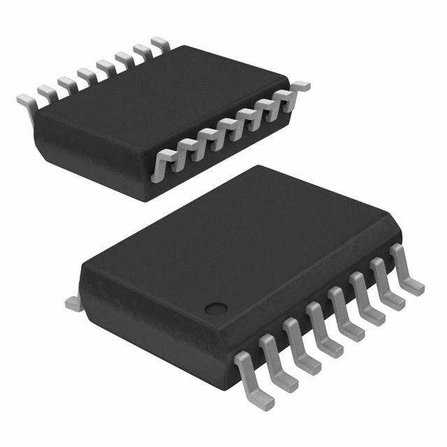
| 供应商器件封装 | 18-SOIC |
| 其它名称 | LTC1325CSWPBF |
| 功能 | 充电管理 |
| 包装 | 管件 |
| 安装类型 | 表面贴装 |
| 封装/外壳 | 18-SOIC(0.295",7.50mm 宽) |
| 工作温度 | 0°C ~ 70°C |
| 标准包装 | 40 |
| 电压-电源 | 4.5 V ~ 16 V |
| 电池化学 | 铅酸,锂离子,镍镉,镍氢 |


PDF Datasheet 数据手册内容提取
LTC1325 Microprocessor-Controlled Battery Management System FEATURES DESCRIPTIOUN n Fast Charge Nickel-Cadmium, Nickel-Metal-Hydride, The LTC®1325 provides the core of a flexible, cost-effec- m Lithium Ion or Lead-Acid Batteries under P Control tive solution for an integrated battery management sys- n Flexible Current Regulation: tem. The monolithic CMOS chip controls the fast charging – Programmable 111kHz PWM Current Regulator of nickel-cadmium, nickel-metal-hydride, lead-acid or with Built-In PFET Driver lithium batteries under microprocessor control. The de- – PFET Current Gating for Use with External Current vice features a programmable 111kHz PWM constant Regulator or Current Limited Transformer current source controller with built-in FET driver, 10-bit n Discharge Mode ADC, internal voltage regulator, discharge-before-charge n Measures Battery Voltage, Battery Temperature and controller, programmable battery voltage attenuator and Ambient Temperature with Internal 10-Bit ADC an easy-to-use serial interface. n Battery Voltage, Temperature and Charge Time The chip may operate in one of five modes: power shut- Fault Protection down, idle, discharge, charge or gas gauge. In power n Built-In Voltage Regulator and Programmable shutdown the supply current drops to 30m A and in the idle Battery Attenuator m mode, an ADC reading may be made without any switching n Easy-to-Use 3- or 4-Wire Serial P Interface noise affecting the accuracy of the measurement. In the n Accurate Gas Gauge Function discharge mode, the battery is discharged by an external n Wide Supply Range: V = 4.5V to 16V DD transistor while the battery is being monitored by the n Can Charge Batteries with Voltages Greater Than V DD LTC1325 for fault conditions. The charge mode is termi- n Can Charge Batteries from Charging Supplies Greater nated by the m P while monitoring any combination of Than V DD battery voltage and temperature, ambient temperature n Digital Input Pins Are High Impedance in and charge time. The LTC1325 also monitors the battery Shutdown Mode for fault conditions before and during charging. In the gas APPLICATIOUNS gauge mode the LTC1325 allows the total charge leaving the battery to be calculated. n System Integrated Battery Charger , LTC and LT are registered trademarks of Linear Technology Corporation. TYPICAL APPLICATIONU Battery Charger for up to 8 NiCd or NiMH Cells VDD(cid:13) 4.5V TO 16V + C2(cid:13) P1(cid:13) 10m F IRF9730 D1(cid:13) 1N6818(cid:13) (cid:13) LTC1325 (e.gM. P80U5(cid:13)1) + CREG(cid:13) 1(cid:13) REG(cid:13) VDD(cid:13) 18(cid:13) R13 L1(cid:13) RTRK 4.7m F 2(cid:13) DOUT(cid:13) PGATE(cid:13) 17(cid:13) R5 62m H 3(cid:13) 16(cid:13) p1.4 4(cid:13) DIN(cid:13) DIS(cid:13) 15(cid:13) 100Ω p1.3 CS(cid:13) VBAT(cid:13) 5(cid:13) 14(cid:13) p1.2 R1 6(cid:13) CLTLFK(cid:13)(cid:13) TTABMABT(cid:13)(cid:13) 13(cid:13) + C0.11(cid:13)m F THERM 1 RDIS 7(cid:13) MCV(cid:13) VIN(cid:13) 12(cid:13) C22RmEGF(cid:13) BAT R2 8(cid:13) HTF(cid:13) SENSE(cid:13) 11(cid:13) THERM 2 IRFZN314(cid:13) 9(cid:13) 10(cid:13) GND FILTER R3 (cid:13) (cid:13) CF(cid:13) 1m F RSENSE R4 LTC1325 • TA01 1
LTC1325 ABSOLUTE WMAXIWMUWM RATINUGS PACKAGE/ORDER IUNFORWMATIOUN (Notes 1, 2) ORDER PART TOP VIEW VDD to GND............................................................. 17V NUMBER All Other Pins................................ –0.3V to V + 0.3V REG(cid:13) 1(cid:13) 18(cid:13) VDD(cid:13) DD Operating Temperature Range.....................0(cid:176) C to 70(cid:176) C DOUT(cid:13) 2(cid:13) 17(cid:13) PGATE(cid:13) Storage Temperature Range................. –65(cid:176) C to 150(cid:176) C DIN(cid:13) 3(cid:13) 16(cid:13) DIS(cid:13) LTC1325CN CS(cid:13) 4(cid:13) 15(cid:13) VBAT(cid:13) LTC1325CSW Lead Temperature (Soldering, 10 sec)..................300(cid:176) C CLK(cid:13) 5(cid:13) 14(cid:13) TBAT(cid:13) LTF(cid:13) 6(cid:13) 13(cid:13) TAMB(cid:13) MCV(cid:13) 7(cid:13) 12(cid:13) VIN(cid:13) HTF(cid:13) 8(cid:13) 11(cid:13) SENSE(cid:13) GND 9 10 FILTER N PACKAGE(cid:13) SW PACKAGE(cid:13) 18-LEAD PDIP 18-LEAD PLASTIC SO WIDE TJMAX = 125(cid:176)C, q JA = 75(cid:176)C/W (N) TJMAX = 125(cid:176)C, q JA = 100(cid:176)C/W (SW) Consult factory for Industrial and Military grade parts. ELECTRICAL CHARACTERISTICS V = 12V – 5%, T = 25(cid:176) C, unless otherwise noted. DD A SYMBOL PARAMETER CONDITIONS MIN TYP MAX UNITS V V Supply Voltage l 4.5 16 V DD DD I V Supply Current All TTL Inputs = 0V or 5V, No Load on REG l 1200 2000 m A DD DD I V Supply Current Power-Down Mode, All TTL Inputs = 0V or 5V l 30 50 m A PD DD V Regulator Output Voltage No Load l 3.047 3.072 3.097 V REG LD Regulator Load Regulation Sourcing Only, I = 0mA to 2mA –1 –5 mV/mA REG REG LI Regulator Line Regulation No Load, V = 4.5V to 16V –60 –100 m V/V REG DD TC Regulator Output Tempco No Load, 0(cid:176) C < T < 70(cid:176) C 50 ppm/(cid:176) C REG A V DACOutput Voltage VR1 = 1, VR0 = 1, 100% Duty Ratio, I = I (Note 7) 140 160 180 mV DAC CHRG VR1 = 1, VR0 = 0, 100% Duty Ratio, I = I/3 48 55 62 mV CHRG VR1 = 0, VR0 = 1, 100% Duty Ratio, I = I/5 30 34 38 mV CHRG VR1 = 0, VR0 = 0, 100% Duty Ratio, I = I/10 16 18 21 mV CHRG V Fault Comparator Hysteresis V = 1V, V = 0.9V, V = 100mV – 20 mV HYST HTF EDV BATR V = V = 2V – 10 mV MCV LTF V Fault Comparator Offset V = 1V, V = 0.9V, V = 100mV – 50 mV OS HTF EDV BATR V = V = 2V MCV LTF V V for BATR = 1 100 mV BATR BAT V V for BATP = 1 l V – 1.8 V BATP BAT DD V Internal EDV Voltage l 860 900 945 mV EDV V , V LTF, MCV Voltage Range 1.6 2.8 V LTF MCV V HTF Voltage Range 0.5 1.3 V HTF A Gas Gauge Gain –0.4V < V < 0V –4 GG SENSE V Gas Gauge Offset –0.4V < V < 0V (Note 6) – 1 LSB OS(GG) SENSE R Internal Filter Resistor 1000 W F TOL Battery Divider Tolerance All Division Ratios l –2 2 % BATD V Input Low Voltage CLK, CS, D l 0.8 1.3 V IL IN V Input High Voltage CLK, CS, D l 1.7 2.4 V IH IN I Low Level Input Current V , V or V = 0V l –2.5 2.5 m A IL CLK CS DIN I High Level Input Current V , V or V = 5V l –2.5 2.5 m A IH CLK CS DIN 2
LTC1325 ELECTRICAL CHARACTERISTICS V = 12V – 5%, T = 25(cid:176) C, unless otherwise noted. DD A SYMBOL PARAMETER CONDITIONS MIN TYP MAX UNITS V Output Low Voltage D , I = 1.6mA l 0.4 V OL OUT OUT V Output High Voltage D , I = –1.6mA l 2.4 V OH OUT OUT I Hi-Z Output Leakage V = 5V l – 10 m A OZ CS V DIS or PGATE Output High V = 4.5V to 16V l V – 0.05 V OHFET DD DD V DIS or PGATE Output Low V = 4.5V to 16V l 0.05 V OLFET DD t Delay Time, CLKfl to D Valid See Test Circuits l 650 ns dDO OUT t Delay Time, CS› to D Hi-Z See Test Circuits l 510 ns dis OUT t Delay Time, CLKfl to D Enabled See Test Circuits l 400 ns en OUT t Time D Remains Valid After CLKfl See Test Circuits l 30 ns hDO OUT t D Rise Time See Test Circuits l 250 ns rDOUT OUT t D Fall Time See Test Circuits l 100 ns fDOUT OUT f Serial I/O Clock Frequency CLK Pin l 25 500 kHz CLK t PGATE Rise Time C = 1500pF l 150 ns rPGATE LOAD t PGATE Fall Time C = 1500pF l 150 ns fPGATE LOAD f Internal Oscillator Frequency Charge Mode, Fail-Safes Disabled 90 111 130 kHz OSC A/D Converter Offset Error V Channel (Note 3) l – 2 LSB IN Linearity Error V Channel (Notes 3, 4) l – 0.5 LSB IN Full-Scale Error V Channel (Note 3) l – 1 LSB IN On-Channel Leakage V Channel ON Only (Notes 3, 5) l – 10 m A IN Off-Channel Leakage V Channel OFF (Notes 3, 5) l – 10 m A IN RECOW W EU DED CHARACTERISTICS SYMBOL PARAMETER CONDITIONS MIN TYP MAX UNITS t Hold Time, D After CLK› 150 ns hDI IN t Setup Time, CS Before First CLK› 1 m s dsuCS t Setup Time, D Stable Before First CLK› 400 ns dsuDI IN t CLK High Time 0.8 m s WHCLK t CLK Low Time 1 m s WLCLK t CS High Time Between Data Transfers 1 m s WHCS t CS Low Time During Data Transfer MSBF = 1 43 CLK Cycles WLCS MSBF = 0 52 CLK Cycles The l denotes specifications which apply over the full operating Note 4: Linearity error is specified between the actual end points of the temperature range. A/D transfer curve. Note 1: Absolute Maximum Ratings are those values beyond which the life Note 5: Channel leakage is measured after channel selection. of a device may be impaired. Note 6: Gas gauge offset excludes A/D offset error. Note 2: All voltage values are with respect to the GND pin. Note 7: I = V (Duty Ratio)/R , where V is the DAC output DAC SENSE DAC Note 3: V within specified min and max limits, CLK (Pin 5) = 500kHz, voltage with control bits VR1 = VR0 = 1, duty ratio = 1 and R is REG SENSE unless otherwise stated. ADC clock is the serial CLK. determined by the user. 3
LTC1325 TYPICAL PERFORWMAUNCE CHARACTERISTICS Regulator Output Voltage vs Regulator Output Voltage vs V Supply Current vs DD Load Current Temperature Temperature 3.077 3.082 1000(cid:13) TA = 27°C(cid:13) 3.081 IREG = 0 900(cid:13) V) 3.076 V) R OUTPUT VOLTAGE ( 333...000777435 VDD =VV 1DD6DDV == 41.25VV R OUTPUT VOLTAGE ((cid:13)33333.....000007777886790 VDD = 12VVDVDD =D 4 =.5 1V6V mPPLY CURRENT (A) 876540000000000(cid:13)(cid:13)(cid:13)(cid:13)(cid:13) VDD = 12V VVDDDD == 146.5VV O O U GULAT 3.072 GULAT 33..007754 V SDD 320000(cid:13)(cid:13) RE 3.071 RE 3.073 100(cid:13) 3.070 3.072 0 0 0.5 1.0 1.5 2.0 2.5 3.0 3.5 4.0 0 10 20 30 40 50 60 70 80 90 0 10 20 30 40 50 60 70 80 90 LOAD CURRENT (mA) TEMPERATURE (°C) TEMPERATURE (°C) 1325 G01 1325 G02 1325 G03 (cid:13) DAC Output Voltage vs Charge Current vs Battery Voltage Temperature Shutdown Current vs Temperature 160(cid:13) 180(cid:13) 25 VR1 = 1, VR0 = 1 VR1 = 1, VR0 = 1 140(cid:13) 160(cid:13) RRENT (mA)11208000(cid:13)(cid:13)(cid:13) VL D=D 1 =0 01m2HV,, RP1S:E NIRSFE9 =5 311W ,(cid:13)(cid:13) VOLTAGE (mV)111420000(cid:13)(cid:13)(cid:13) VDD = 12V mURRENT (A) 2105 VVDDDD == 1162VV CHARGE CU 6400(cid:13)(cid:13) VVRR11 == 10,, VVRR00 == 01 DAC OUTPUT 864000(cid:13)(cid:13)(cid:13) VVRR11 == 10,, VVRR00 == 01 SHUTDOWN C 105 20(cid:13) VR1 = 0, VR0 = 0 20(cid:13) VR1 = 0, VR0 = 0 VDD = 4.5V 0 0 0 0 2 4 6 8 10 12 0 10 20 30 40 50 60 70 0 10 20 30 40 50 60 70 80 90 BATTERY VOLTAGE (V) TEMPERATURE (°C) TEMPERATURE (°C) 1325 G04 1325 G05 1325 G06 Fault Comparator Threshold vs Fault Comparator Threshold vs Gas Gauge Gain and Offset vs Temperature Temperature Temperature 1.0 11(cid:13) 0 HRESHOLD (V) 0000....6789 VCELL FOR EDV = HIGH HRESHOLD (V) 10987(cid:13)(cid:13)(cid:13)(cid:13) VBAT FOR BATP = HIGH, VDD = 12V FSET (COUNTS)–––110...505 VIWNSICETLNHUS ETD E=EM S– PC0E.H2RAVAN TAGUNERDSE –IN0 .V4RVE(cid:13)G (cid:13) ATOR T 0.5 ATOR T 6(cid:13) VCELL FVOTRB AMT CFVO R= LHTIGF H=, HVIMGCHV, =V L2T.F8 V= 2A.N8DV(cid:13) AND OF––22..50 GAS GAUGE OFFSET FAULT COMPAR 0000....3421 VTBATV FCOERLL H FTOFR = B HAITGRH ,= V HHITGFH = 0.4V FAULT COMPAR 5432(cid:13)(cid:13)(cid:13)(cid:13) VTBAVTC VFETOLBLRA F THO FTROF RM= CLHVTIGF = H= H, HVIGIHGHTH,F ,V= VM 1LCT.3VF5 ==V 11..66VV(cid:13) AS GAUGE GAIN –––334...500 GAS GAUGE GAIN G 0 1 –4.5 0 10 20 30 40 50 60 70 80 0 10 20 30 40 50 60 70 80 0 10 20 30 40 50 60 70 80 TEMPERATURE (°C) TEMPERATURE (°C) TEMPERATURE (°C) 1325 G07 1325 G08 1325 G09 4
LTC1325 TYPICAL PERFORWMAUNCE CHARACTERISTICS PGATE Rise Time vs PGATE Fall Time vs Load Capacitance Load Capacitance Differential Nonlinearity 1200 1000 1.0(cid:13) 900 VDD = 12V(cid:13) 1000 800 LSB) fCLK = 500kHz GATE RISE TIME (ns) 486000000 TA = 70T°CAT A= =2 70°°CC GATE FALL TIME (ns) 753460000000000 TA = 70T°AC =T 2A7 =°C 0°C NTIAL NONLINEARITY ( 0.50(cid:13)(cid:13) P P RE–0.5(cid:13) 200 E 200 FF 100 DI 0 0 –1.0 0 2 4 6 8 10 12 14 16 18 20 0 2 4 6 8 10 12 14 16 18 20 0 128 256 384 512 640 768 896 1024 LOAD CAPACITANCE (nF) LOAD CAPACITANCE (nF) CODE 1325 G10 LTC1325 G11 1325 G12 Discharge Rise and Fall Time Minimum Charging Supply vs vs Load Capacitance Number of Cells Integral Nonlinearity 14 16(cid:13) 1.0(cid:13) mDISCHARGE RISE AND FALL TIME (s) 11842602 TTTAAA === 72007°C°°CC(cid:13)(cid:13)(cid:13) RISFEA LTLIM TEIME MINIMUM CHARGE VOLTAGE (V) 1114208642(cid:13)(cid:13)(cid:13)(cid:13)(cid:13)(cid:13)(cid:13) TAR =S IE2RN7FS°9ECZ ,=3 N 00iP.CRLI1LRF dS5= EF =E, BT9 2 NV1,AZ5 SR013TmEmN01T H=P HE5= RF81T TE11,OI OET,9V VS1 , R1 RD0(cid:13)1010I0NO0 m=5=mD H8 1H1E1(cid:13),(cid:13)(cid:13) 9V RD0IO =D 1E(cid:13) INTEGRAL NONLINEARITY (LSB)–00..505(cid:13)(cid:13)(cid:13) VfCDLDK == 1520V0(cid:13)kHz VCELL = 1.4V NOMINAL 0 0 –1.0 0 2 4 6 8 10 12 14 16 18 20 1 2 3 4 5 6 7 8 0 128 256 384 512 640 768 896 1024 LOAD CAPACITANCE (nF) NUMBER OF CELLS CODE 1325 G13 1325 G14 1325 G15 (cid:13) Oscillator Frequency vs CLK to D Enable Delay Time CLK to D Valid Delay Time OUT OUT Temperature vs Temperature vs Temperature 118 500 700 OSCILLATOR FREQUENCY (kHz)111111111111111110412350679 CLK TO D ENABLE DELAY TIME (ns)OUT31223144050550055000000000 CLK TO D VALID DELAY TIME (ns)OUT 463215000000000000 DOUT GOING HIGH DOUT GOING LOW 108 0 0 –40 –20 0 20 40 60 80 100 0 10 20 30 40 50 60 70 80 0 10 20 30 40 50 60 70 80 TEMPERATURE (°C) TEMPERATURE (°C) TEMPERATURE (°C) 1325 G16 1325 G17 1325 G18 5
LTC1325 PIUN FUUNCTIOUNS REG (Pin 1): Internal Regulator Output. The regulator SENSE (Pin 11): The Sense pin controls the switching of provides a steady 3.072V to the internal analog circuitry the 111kHz PWM constant current source in the charging and provides a temperature stable reference voltage for mode. The Sense pin is connected to an external sense generating MCV, HTF, LTF and thermistor bias voltages resistor R and the negative side of the battery. The SENSE with external resistors. Requires a 4.7m F or greater bypass charging loop forces the average voltage at the Sense pin capacitor to ground. to equal a programmable internal reference voltage V . DAC The battery charging current is equal to V /R . D (Pin 2): TTL Data Output Signal for the Serial DAC SENSE OUT Interface. D and D may be tied together to form a In the gas gauge mode the voltage across the Sense pin OUT IN 3-wire interface, or remain separated to form a 4-wire is filtered by an RC network (R and C ), amplified by F F interface. Data is transmitted on the falling edge of CLK an inverting gain of four, then multiplexed to the ADC so (Pin 5). the average discharge current through the battery may be measured and the total charge leaving the battery D (Pin 3): TTL Data Input Signal for the Serial Interface. IN calculated. The data is latched into the chip on the rising edge of the CLK (Pin 5). V (Pin 12): General Purpose ADC Input. IN CS (Pin 4): TTL Chip Select Signal for the Serial Interface. T (Pin 13): Ambient Temperature Input. Connect to an AMB external thermistor network. Tie to REG if not used. May CLK (Pin 5): TTL Clock for the Serial Interface. be used as another general purpose ADC input. LTF (Pin 6): Minimum Allowable Battery Temperature T (Pin 14): Battery Temperature Input. Connect to an Analog Input. LTF may be generated by a resistive divider BAT external NTC thermistor network. Tie to REG if not used. between REG (Pin 1) and ground. V (Pin 15): Battery Input. An internal voltage divider is MCV (Pin 7): Maximum Allowable Cell Voltage Analog BAT connected between the V and Sense pins to normalize Input. MCV may be generated by a resistive divider be- BAT all battery measurements to one cell voltage. The divider tween REG (Pin 1) and ground. is programmable to the following ratios: 1/1, 1/2, 1/3 . . . HTF (Pin 8): Maximum Allowable Battery Temperature 1/15, 1/16. In shutdown and gas gauge modes the divider Analog Input. HTF may be generated by a resistive divider is disconnected. between REG (Pin 1) and ground. DIS (Pin 16): Active High Discharge Control Pin. Used GND (Pin 9): Ground. to turn on an external transistor which discharges the battery. FILTER (Pin 10): The external filter capacitor C is con- F nected to this pin. The filter capacitor is connected to the PGATE (Pin 17): FET Driver Output. Swings from GND output of the internal resistive divider across the battery to to V . DD reduce the switching noise while charging. In the gas V (Pin 18): Positive Supply Voltage. 4.5V < V < 16V. gauge mode, C along with an internal R = 1k form a DD DD F F lowpass filter to average the voltage across the sense resistor. 6
LTC1325 BLOCK DIAGRAWM 18 VDD 5V(cid:13) DIGITAL INPUT CIRCUITS PS 3.072V(cid:13) 1 DIGITAL(cid:13) ANALOG(cid:13) REG REGULATOR REGULATOR ANALOG AND DIGITAL VDD(cid:13) ADC REFERENCE 16 DIS BATP, BATR, FMCV,(cid:13) GND 9 FEDV, FHTF, FLTF, tOUT tOUT 6 LTF 7 8 HTF CLK 5 CONTROL(cid:13) MOD0 TO MOD1, PS DFEATUELCTT(cid:13)(cid:13) 7 MCV CS 4 SERIAL(cid:13) LOGIC 3 CIRCUITRY DIN 3 I/O 2 DOUT 2 PS, MSBF 3 DS0 TO DS1(cid:13) 10 SGL/DIFF 12 VIN 13 TAMB 14 TBAT 15 DIV0 TO DIV3 VBAT 4 10-BIT(cid:13) ADC(cid:13) A/D CONVERTER MUX 5 MOD0 TO MOD1, VR0 TO VR1, PS CHARGE GAS GAUGE 11 SENSE 10 FILTER 17 PGATE CHARGE LOOP(cid:13) PS 111kHz(cid:13) AND(cid:13) DIVIDER OSCILLATOR GAS GAUGE TOUT DR0 TO DR3 3 DUTY RATIO(cid:13) TIMEOUT LOGIC 3 GENERATOR LTC1325 • BD TO0 TO TO2 TEST CIRC(cid:13)UITS (cid:13) Load Circuit for t , t and t Load Circuit for t and t dDO r f dis en 1.4V TEST POINT 3k 3k 5V tdis WAVEFORM 2, ten DOUT DOUT 100pF 100pF tdis WAVEFORM 1 LTC1325 • TC01 LTC1325 • TC02 7
LTC1325 TEST CIRC(cid:13)UITS (cid:13) Voltage Waveforms for D Delay Time, t Voltage Waveforms for D Rise and Fall Times, t, t OUT dDO OUT r f 2.4V CLK 0.8V 0.4V tdDO 2.4V tr tf DOUT LTC1325 • TC04 0.4V LTC1325 • TC03 On and Off Channel Leakage Voltage Waveforms for t dis 3.072V 2V ION CS A ON CHANNEL DOUT(cid:13) WAVEFORM 1(cid:13) IOFF (SEE NOTE 1) 90% A }OFF(cid:13) CHANNELS tdis DOUT(cid:13) 10% WAVEFORM 2(cid:13) (SEE NOTE 2) NOTE: EXTERNAL CHANNELS ONLY––(cid:13) NOTE 1: WAVEFORM 1 IS FOR AN OUTPUT WITH INTERNAL CONDITIONS (cid:13) TBAT, TAMB AND VIN LTC1325 • TC05 SUCH THAT THE OUTPUT IS HIGH UNLESS DISABLED BY CS.(cid:13) NOTE 2: WAVEFORM 2 IS FOR AN OUTPUT WITH INTERNAL CONDITIONS (cid:13) SUCH THAT THE OUTPUT IS LOW UNLESS DISABLED BY CS. LTC1325 • TC06 Voltage Waveforms for t en CS DIN START VR1 CLK 1 21 22 23 0.4V 24 ten THREE-STATE NULL DOUT D9 0.4V LTC1325 • TC07 8
LTC1325 TI W (cid:13)I U G DIAGRAW MSB-FIRST DATA (MSBF = 1) CS CLK START MSBF DIN NULL BATP FS HI-Z HI-Z DOUT D9 D1D0 COMMAND WORD ADC DATA STATUS WORD MSB-FIRST DATA (MSBF = 0) CS CLK START VR1 DIN NULL BATP FS HI-Z HI-Z DOUT D9 D1D0 D1 D9 COMMAND WORD ADC DATA STATUS WORD LTC1325 • TD NOTE: THE TIMING DIAGRAM SHOWS TWO POSSIBLE COMMAND WORDS.(cid:13) REFER TO FUNCTIONAL DESCRIPTION FOR INFORMATION ON HOW TO(cid:13) CONSTRUCT THE COMMAND WORD FUUNCTIOUNAL DESCRIPTIOU GENERAL DESCRIPTION During normal operation, a command word is shifted into During the discharge mode, the battery is discharged by the chip via the serial interface, then an ADC measurement an external transistor and series resistor. The battery is is made and the 10-bit reading and chip status word are monitored for fault conditions. shifted out. The command word configures the LTC1325 In the charge mode, the m P monitors the battery’s voltage, and forces it into one of five modes: power shutdown, idle, temperature and ambient temperature via the 10-bit ADC. discharge, charge or gas gauge mode. Termination methods such as –D V , D V /D Time, BAT BAT In the power shutdown mode, the analog section is turned D T , D T /D Time, D (T – T ), maximum tempera- BAT BAT BAT A off and the supply current drops to 30m A. The voltage ture, maximum voltage and maximum charge time may be regulator, which provides power to the internal analog accurately implemented in software. The LTC1325 also circuitry and external bias networks, is shut down. The monitors the battery for fault conditions. voltage divider across the battery is disconnected and only In the gas gauge mode, the average voltage across the the voltage regulator for the serial interface logic is left on. sense resistor can be measured to determine the average During the idle mode, the chip is fully powered but the battery load current. The sense voltage is filtered by an RC discharge, charge, and gas gauge circuits are off. The chip circuit, multiplied by an inverting gain of four, then con- may be placed in the idle mode momentarily while charg- verted by the ADC. The m P can then accumulate the ADC ing the battery, allowing an ADC measurement to be made measurements and do a time average to determine the without any switching noise from the PWM current source total charge leaving the battery. The RC circuit consists of affecting the accuracy of the reading. The mode command an internal 1k resistor R and an external capacitor C F F bits are picked off as they appear at D , allowing the connected to the Filter pin. IN charging loop to turn off and settle while the remainder of the command word is being shifted in. 9
LTC1325 FUUNCTIOUNAL DESCRIPTIOU COMMAND WORD Bit 5: MSB-First/LSB-First (MSBF) The command word is 22 bits long and contains all the The ADC data is programmed for MSB-first or LSB-first information needed to configure and control the chip. On sequence using the MSBF bit. See Serial I/O description power-up all bits are cleared to logical “0.” for details. 1 2 3 4 5 6 7 8 MSBF DESCRIPTION START(cid:13) SGL/(cid:13) MOD0 MOD1 MSBF DS0 DS1 DS2 0 LSB-First Data Follows MSB-First Data = 1 DIFF 1 MSB-First Data Only 9 10 11 12 13 14 15 16 DIV0 DIV1 DIV2 DIV3 PS DR0 DR1 DR2 Bits 6 to 8: ADC Data Input Select (DS0 to DS2) DS2, DS1 and DS0 select which circuit is connected to the 17 18 19 20 21 22 ADC input. Do not use unlisted combinations. FSCLR TO0 TO1 TO2 VR0 VR1 LTC1325 • F01 DS2 DS1 DS0 DESCRIPTION Figure 1. Command Word 0 0 0 Gas Gauge Output Bit 1: Start Bit (Start) 0 0 1 Battery Temperature Pin, T BAT 0 1 0 Ambient Temperature Pin, T The first “logical one” clocked into the D input after CS AMB IN 0 1 1 Battery Divider Output Voltage, V goes low is the start bit. The start bit initiates the data CELL 1 0 0 V Pin transfer and all leading zeros which precede this logical IN one will be ignored. After the start bit is received, the Bits 9 to 12: Battery Divider Ratio Select (DIV0 to DIV3) remaining bits of the command word will be clocked in. DIV3, DIV2, DIV1 and DIV0 select the division ratio for the Bits 2 and 3: Mode Select (MOD0 and MOD1) voltage divider across the battery. The two mode bits determine which of four modes the chip DIV3 DIV2 DIV1 DIV0 DESCRIPTION will be in: idle, discharge, charge or gas gauge. 0 0 0 0 (V – V )/1 BAT SENSE 0 0 0 1 (V – V )/2 MOD1 MOD0 DESCRIPTION BAT SENSE 0 0 1 0 (V – V )/3 0 0 Idle BAT SENSE 0 0 1 1 (V – V )/4 0 1 Discharge BAT SENSE 0 1 0 0 (V – V )/5 1 0 Charge BAT SENSE 0 1 0 1 (V – V )/6 1 1 Gas Gauge BAT SENSE 0 1 1 0 (V – V )/7 BAT SENSE 0 1 1 1 (V – V )/8 Bit 4: Single-Ended Differential Conversion (SGL/DIFF) BAT SENSE 1 0 0 0 (V – V )/9 BAT SENSE SGL/DIFF determines whether the ADC makes a single- 1 0 0 1 (V – V )/10 BAT SENSE ended measurement with respect to ground or a differen- 1 0 1 0 (V – V )/11 BAT SENSE tial measurement with respect to the Sense pin. 1 0 1 1 (V – V )/12 BAT SENSE 1 1 0 0 (V – V )/13 BAT SENSE SGL/DIFF DESCRIPTION 1 1 0 1 (V – V )/14 BAT SENSE 0 Single-Ended ADC Conversion 1 1 1 0 (V – V )/15 BAT SENSE 1 Differential ADC Conversion (with respect to Sense) 1 1 1 1 (V – V )/16 BAT SENSE 10
LTC1325 FUUNCTIOUNAL DESCRIPTIOU Bits 21 and 22: Charging Loop Reference Voltage Bit 13: Power Shutdown (PS) Select (VR0 and VR1) PS selects between the normal operating mode, or the VR1 and VR0 select the desired reference voltage V CHRG shutdown mode. for the charging loop. The charging loop will force the average voltage at the Sense pin to be equal to V . The PS DESCRIPTION DAC average charging current is V /R (see Figure 4). 0 Normal Operation DAC SENSE 1 Shutdown All Circuits Except Digital Inputs VR1 VR0 V (mV) DAC 0 0 18 Bits 14 to 16: Duty Ratio Select (DR0 to DR2) 0 1 34 DR2, DR1 and DR0 select the duty cycle of the charging 1 0 55 loop operation (not 111kHz PWM duty cycle). The last 1 1 160 three selections place the chip into a test mode and should not be used. STATUS WORD DR2 DR1 DR0 DESCRIPTION The status word is 8 bits long and contains the status of 0 0 0 1/16 the internal fail-safe circuits. 0 0 1 1/8 0 1 0 1/4 0 1 1 1/2 1 2 3 4 5 6 7 8 1 0 0 1 BATP BATR FMCV FEDV FHTF FLTF tOUT FS 1 0 1 Test Mode 1 LTC1325 • F02 1 1 0 Test Mode 2 1 1 1 Test Mode 3 Figure 2. Status Word Bit 17: Fail-Safe Latch Clear (FSCLR) Bit 1: Battery Present (BATP) When FSCLR bit is set to one, the internal fail-safe timer is The BATP bit = 1 indicates the presence of the battery. The reset to 0, and the fail-safe latches are reset. FSCLR is bit is set to 1 when the voltage at the V pin falls below BAT automatically reset to 0 when CS goes high. (V – 1.8V). BATP = 0 when the battery is removed and DD V is pulled high by R (see Figure 3). FSCLR DESCRIPTION BAT TRK 0 No Action BATP CONDITIONS 1 Reset Fail-Safe Timer and Latches 0 (V – 1.8) < V < V DD BAT DD 1 V < (V – 1.8) Bits 18 to 20: Timeout Period Select (TO0 to TO2) BAT DD TO2, TO1 and TO0 select the desired fail-safe timeout Bit 2: Battery Reversed (BATR) or Shorted period,t . On power-up, the default timeout is 5 minutes. OUT The BATR bit indicates when the battery is connected backwards or shorted. The bit is set when the battery cell TO2 TO1 TO0 TIMEOUT (MINUTES) 0 0 0 5 voltage at the output of the battery divider VCELL is below 0 0 1 10 100mV. 0 1 0 20 0 1 1 40 BATR CONDITIONS 1 0 0 80 0 V > 100mV CELL 1 0 1 160 1 V < 100mV CELL 1 1 0 320 1 1 1 Indefinite (No Timeout) 11
LTC1325 FUUNCTIOUNAL DESCRIPTIOU Bit 3: Maximum Cell Voltage (FMCV) T CONDITIONS OUT The MCV bit indicates when the battery cell voltage has 0 No Timeout Has Occurred 1 Timeout Has Occurred exceeded the preset limit. The bit is set when V is CELL greater than the voltage at the MCV pin. Bit 8: Fail-Safe Occurred (FS) FMCV CONDITIONS The FS bit indicates that one of the fault detection circuits 0 V < V CELL MCV halted the discharging or charging cycle. The bit is set 1 V > V CELL MCV when an EDV, LTF, HTF, or t fault occurs during OUT discharge. During charging, the bit is set when a MCV, Bit 4: End Discharge Voltage (FEDV) LTF, HTF, or t fault occurs. The bit is reset by the OUT The EDV bit indicates when the battery cell voltage has command word bit FSCLR. dropped below an internally preset limit. The bit is set when the battery cell voltage at the output of the voltage FS CONDITIONS divider V is less than 900mV. 0 No Fail-Safe Has Occurred CELL 1 Fail-Safe Has Occurred FEDV CONDITIONS 0 V > 900mV CELL DETAILED DESCRIPTION 1 V < 900mV CELL Fault Conditions Bit 5: High Temperature Fault (FHTF) The LTC1325 monitors the battery for fault conditions The HTF bit indicates when the battery temperature is too before and during discharge and charge (see Figure 3). high. Using a negative TC thermistor, the bit is set when They include: battery removed/present (BATP), battery the voltage at the TBAT pin is less than the voltage at the reversed/shorted (BA(cid:13) TR), maximum cell voltage exceeded HTF pin. VDD FHTF CONDITIONS VDD 0 T > V 1.8V 3.072V(cid:13) REG RTRK BAT HTF + LINEAR(cid:13) 1 TBAT < VHTF C1 – REGULATOR BATP –+ VBAT R1 Bit 6: Low Temperature Fault (FLTF) PROGRAMMABLE(cid:13) R2 The LTF bit indicates when the battery temperature is too BATTERY(cid:13) DIVIDER low. Using a negative TC thermistor, the bit is set when the C2 voltage at the T pin is greater than the voltage at the + SENSE BAT FMCV – REG MCV LTF pin. C3 FLTF CONDITIONS FEDV –+ 900mV R3 RL 0 TBAT < VLTF C4 + 100mV 1 TBAT > VLTF BATR – C5 TBAT Bit 7: Timeout (t ) – OUT FHTF + HTF The tOUT bit indicates that the battery charging time has C6+ R4 RT FLTF – LTF exceeded the preset limit. The bit is set when the internal timer exceeds the limit set by the command bits TO0, TO1 LTC1325 • F03 and TO2. Figure 3. Fail-Safe or Fault Detection Circuitry 12
LTC1325 FUUNCTIOUNAL DESCRIPTIOU (MCV), minimum cell voltage exceeded (EDV), high tem- The chip enters the discharge mode when the proper perature limit exceeded (HTF), low temperature limit ex- mode command bits are set and the power shutdown ceeded (LTF) and time limit exceeded (t ). When a fault command bit is clear. If a fault condition does not exist, OUT condition occurs, the discharge and charge loops are then the DIS pin is pulled up to V by the internal driver. DD disabled or prevented from turning on and the fail-safe bit The DIS voltage is used to turn on an external transistor (FS) is set. The chip is reset by shifting in a new command which discharges the battery through an external series word with the fail-safe clear FSCLR bit set. The 8-bit status resistor R . DIS word contains the state of each fault condition. Discharging will continue until a new command word is input to change the mode or a fault condition occurs. Power Shutdown Mode Command: MOD1 = X, MOD0 = X, PS = 1 Charge Mode Status: BATP = X, BATR = X, FMCV = X, FEDV = X, Command: MOD1 = 1, MOD0 = 0, PS = 0 FHTF = X, FLTF = X, t = X OUT Status: BATP = 1, BATR = 0, FMCV = 0, FEDV = X, In the power shutdown mode, the analog section is turned FHTF = 0, FLTF = 0, t = 0 OUT off and the supply current drops to 30m A. The voltage The chip enters the charge mode when the proper mode regulator, which provides power to the internal analog command bits are set and the power shutdown command circuitry and external bias networks, is shut down. The bit is clear. If a fault condition does not exist then charging voltage divider across the battery is disconnected and the can begin. Charging will continue until a new command only circuit left on is the voltage regulator for the serial word is input to change the mode or a fault condition interface logic. occurs. Idle Mode The charge current may be regulated by a programmable 111kHz PWM buck current regulator, or by using the PFET Command: MOD1 = 0, MOD0 = 0, PS = 0 to gate an external current regulator or current limited Status: BATP = X, BATR = X, FMCV = X, FEDV = X, transformer. FHTF = X, FLTF = X, t = X OUT 111kHz PWM Controller The chip enters the idle mode when the proper mode command bits are set and the power shutdown command The block diagram of the charging loop connected as a bit is cleared. During the idle mode, the chip is fully PWM buck current regulator is shown in Figure 4. The powered, but the discharge, charge and gas gauge circuits PWM may operate in either continuous or discontinuous are off. The chip may be placed in the idle mode momen- mode. The loop forces the average voltage across the tarily while charging the battery, allowing an ADC mea- sense resistor to be equal to the voltage at the output of the surement to be made without any switching noise from the DAC, so that the charging current becomes V /R . DAC SENSE PWM current source affecting the accuracy of the reading. With switch S2 on and the others off, amplifier A1 along The mode command bits are picked off as they appear at with C1, R1 and R2 are configured as an integrator with D , so that while the rest of the command word is being IN 16kHz bandwidth. The output of the integrator is the shifted in, the charging loop has time to settle before an average difference between the voltage across the sense ADC measurement is made. resistor and the DAC output voltage. Discharge Mode The rising edge of the oscillator waveform triggers the one shot which sets the flip-flop output high. This turns on the Command: MOD1 = 0, MOD0 = 1, PS = 0 external PFET P1 by pulling its gate low via the FET driver. Status: BATP = 1, BATR = 0, FMCV = X, FEDV = 0, With P1 on, the current through the inductor L1 starts to FHTF = 0, FLTF = 0, t = 0 OUT 13
LTC1325 FUUNCTIOUNAL DESCRIPTIOU VDD(cid:13) 4.5V TO 16V CHARGE PGATE P1(cid:13) IRF9Z30 RTRK DR0 TO(cid:13) 3 DUTY RATIO(cid:13) DR2 GENERATOR DIS DISCHARGE D1(cid:13) 1N5818 L1 111kHz(cid:13) OSCILLATOR RDIS GG BATTERY ONE SHOT R1(cid:13) R2(cid:13) RF(cid:13) N1(cid:13) S1 500k 125k 1k SENSE IRFZ34 Q S + 1C61p(cid:13)F S2 S4 CF RSENSE FILTER S3 R A2 – – TO(cid:13) REG(cid:13) ADC MUX A1 3.072V + GG(cid:13) VR1(cid:13) VR0(cid:13) DAC VOLTAGE(cid:13) 0(cid:13) 0(cid:13) 0(cid:13) 18mV(cid:13) 0(cid:13) 0(cid:13) 1(cid:13) 34mV(cid:13) VDAC DAC 0(cid:13) 1(cid:13) 0(cid:13) 55mV(cid:13) 0(cid:13) 1(cid:13) 1(cid:13) 160mV(cid:13) 1 X X 0mV 2 VR0, VR1 GG(cid:13) CHIP(cid:13) (GAS GAUGE)BOUNDARY LTC1325 • F04 Figure 4. Charging Loop Block Diagram rise as does the voltage across the sense resistor. When ample, if a duty ratio of 1/2 is programmed, the generator the voltage across the sense resistor is greater than the output is low only for 42/2 = 21 seconds. Since the loop output of the integrator, comparator A2 changes state. operates for only 21 out of every 42 seconds, the average This resets the flip-flop and P1 is turned off. Catch diode charging current is halved. In general, the average charg- D1 clamps the drain of P1 one diode drop below ground ing current is: when the inductor flies back and the current through the I = V (Duty Ratio)/R CHRG DAC SENSE inductor starts to drop. The voltage across the sense resistor also drops and may reach zero and stay there until Gated PFET Controller the next clock cycle begins. When using an external current regulator or current lim- The average charging current is set by the output of the ited wall pack, simply remove the inductor L1 and catch DAC (V ) and the duty ratio generator. V can be DAC DAC diode D1. Set the DAC control bits VR1 = 1 and VR0 = 1, programmed to one of four values with the following and select the desired duty ratio. By insuring that the ratios: 1, 1/3, 1/5 or 1/10. The duty ratio can be set to voltage at the Sense pin is never greater than 140mV, the 1/16, 1/8, 1/4, 1/2 or 1. When the duty ratio is 1, the duty output of the integrator A1 will saturate high and the ratio generator output is always low and the charge loop comparator A2 will never trip and turn the loop off. This operates continuously (see Figure 4). At other duty ratio can be achieved by removing the sense resistor and settings, the duty generator output is a square wave with grounding the Sense pin or if the gas gauge is to be used, a period of 42 seconds. The time for which the generator selecting R so that R /I < 140mV. SENSE SENSE CHRG output is low varies with the duty ratio setting. For ex- 14
LTC1325 FUUNCTIOUNAL DESCRIPTIOU Gas Gauge Mode duplex operation, D and D may be tied together IN OUT allowing transmission over just three wires: CS, CLK and Command: MOD1 = 1, MOD0 = 1, PS = 0 DATA (D /D ). IN OUT Status: BATP = X, BATR = X, FMCV = X, FEDV = X, Data transfer is initiated by a falling chip select CS signal. FHTF = X, FLTF = X, t = X OUT After CS falls, the LTC1325 looks for a start bit on D . The IN In the gas gauge mode, the average voltage across the start bit is the first “logical one” clocked into the D input IN sense resistor can be measured to determine the average after CS goes low. The LTC1325 will ignore all leading battery load current. The output of the DAC is set to ground zeros which precede this logical one. After the start bit is and switches S1, S3 and S4 are closed. A1 is configured received, the 21 other control bits are shifted into the D IN as an inverting amplifier with R1 and R2 setting the gain pin to configure the LTC1325 and start a conversion. After to –4. The voltage across the sense resistor is filtered by the last command bit, the D pin remains in three-state OUT an RC circuit (RF, CF) amplified by A1, then converted by for one clock period before it is taken low for one null bit. the ADC. Following the null bit, the conversion results and the 8 status bits are shifted out on the D pin. At the end of the The microprocessor can then accumulate the ADC mea- OUT data exchange, CS should be brought high. surements and do a time average to determine the total charge leaving the battery. The Sense pin voltage should MSB-First/LSB-First (MSBF Control Bit) not be more negative than –450mV to ensure linearity. The output data of the LTC1325 is programmed for MSB- The R C circuit consists of an internal 1k resistor and an F F first or LSB-first sequence using the MSFB control bit. external capacitor connected to the Filter pin. R C should F F When MSBF = 1, data will appear on D in MSB-first be longer than the measurement interval. With the serial OUT format. This is followed by the 8 status bits. Logical zeros clock running at 100kHz, it take 380m s to shift in the will be filled in indefinitely following the last data bit to command word and shift out the ADC measurement and accommodate longer word lengths required by some status word. microprocessors. When MSBF = 0, LSB-first data will follow the MSB-first data. Regardless of the state of Trickle Resistor MSBF, the status bits are always shifted out in the same An external trickle resistor has several functions. First, it order (see Figure 2). provides a continuous trickle charge current for topping off the battery and countering the effects of self-discharge. Accommodating Microprocessors with Different Word Second, it can be used to condition a deeply discharged Lengths battery for charging. The LTC1325 will not charge a battery The LTC1325 will fill zeros indefinitely after the transmit- unless its cell voltage is above 100mV (BATR). Finally, the ted data until CS is brought high. At that time D is resistor is required by the battery detect circuit to pull the OUT disabled (three-stated). This makes for easy interfacing V pin high when the battery is removed. BAT to MPU serial ports with different transfer increments including 4 bits (e.g., COP400) and 8 bits (e.g., SPI and SERIAL INTERFACE MICROWIRE/PLUSTM). Any word length can be accom- The LTC1325 communicates with microprocessors and modated by the correct positioning of the start bit in the other external circuitry via a synchronous, half duplex, input word. 4-wire serial interface. The clock CLK synchronizes the Operation with D and D Tied Together data transfer with each bit being transmitted on the falling IN OUT edge and captured on the rising CLK edge in both transmit- The LTC1325 can be operated with D and D tied IN OUT ting and receiving systems. The LTC1325 first receives together. This eliminates one of the lines required to input data and then transmits back the A/D conversion result and status word (half duplex). Because of the half MICROWIRE/PLUS is a trademark of National Semiconductor Corp. 15
LTC1325 FUUNCTIOUNAL DESCRIPTIOU communicate with the microprocessor. Data is transmit- (cid:82) Ø (cid:230) (cid:49) (cid:49) (cid:246) ø ted in both directions on a single wire. The processor pin (cid:84) =(cid:101)(cid:120)(cid:112)Œ b (cid:231) - (cid:247) œ (2) (cid:82) º Ł (cid:84) (cid:84) ł ß connected to this data line should be configurable as either (cid:84)(cid:79) (cid:79) an input or an output. The LTC1325 will take control of the data line and drive it low after the 23rd falling CLK edge (cid:230) b - (cid:50)(cid:84) (cid:246) after the start bit is received. Therefore the processor port (cid:82)(cid:76) =(cid:82)(cid:84)(cid:79)Ł(cid:231) b +(cid:50)(cid:84)(cid:79)ł(cid:247) (3) (cid:79) must be switched to an input before this happens to avoid a conflict. Ø (cid:230) (cid:84) (cid:246) ø (cid:230) (cid:82) (cid:246) b= Œ (cid:84)(cid:231) (cid:79) (cid:247) œ (cid:73)(cid:110)(cid:231) (cid:84) (cid:247) (4) Power-Up After Shutdown º Ł (cid:84)(cid:79) - (cid:84)ł ß Ł (cid:82)(cid:84)(cid:79)ł When a control word with the PS bit set to one is written to the LTC1325, it enters shutdown mode in which the VDD a = (cid:49) (cid:230)(cid:231) (cid:100)(cid:82)(cid:84)(cid:246)(cid:247) (5) supply current is reduced to 30m A. In this mode the on- (cid:82) Ł (cid:100)(cid:84) ł (cid:84) chip 3V regulator and all circuits powered off it are shut down. The only circuits that remain alive are DIN, CS and - b CLK input buffers. To take the LTC1325 out from shut- a = (cid:32) (6) (cid:50) down mode, a high to low edge must be applied to the CS (cid:84) pin. Either D or CLK must be low when CS is low to IN (cid:230) (cid:246) prevent a false control word from being transmitted to the (cid:100)(cid:86) ( ) - b (cid:49) (cid:68)(cid:73)(cid:86) = (cid:86) (cid:84) (cid:231) (cid:177) + (cid:247) LTC1325. The 3V output decays with a time constant of (cid:68)(cid:73)(cid:86) (cid:79) (cid:231) (cid:247) (7) 300ms with C = 4.7m F. The microprocessor should (cid:100)(cid:84) Ł (cid:50)(cid:84)(cid:79)(cid:50) (cid:84)(cid:79)ł REG wait three seconds before applying a wake-up edge to the where, CS pin to ensure proper power-up. V (T) is the output of the divider, DIV TEMPERATURE SENSING V is the voltage at the REG pin (3.072V nominal), REG R is the thermistor resistance at some temperature T, NTC (Negative Temperature Coefficient) Thermistors T R is the thermistor resistance at some reference The simplest method to sense temperature (battery or TO temperature T , ambient) with an NTC thermistor is to use a voltage divider O powered by the REG pin. This divider consists of a load b is a constant dependent on thermistor material, resistor R in series with a thermistor R as shown in L T a is the temperature coefficient (in %/(cid:176) C) of R at Figure 3. For a given thermistor, there is a value of R T L T , and which makes V (T) linear over a narrow but adequate O DIV temperature range. The easiest method (Inflection Point all temperatures are in (cid:176) K (i.e., T(cid:176) C + 273) Method) to calculate R is to set the second temperature L There are two assumptions in the derivation of the above derivative of the divider output to 0. The equations relevant equations. b is assumed to be constant and the tempera- to this method are: ture coefficient of R is small compared to that of the L ( ) thermistor. (cid:86)(cid:68)(cid:73)(cid:86) (cid:84) (cid:49) ( ) (cid:86) = (cid:230) (cid:49)+(cid:82) (cid:246) = (cid:102) (cid:84)(cid:32) Most thermistor data sheets specify RTO, b , RT/RTO ratios (cid:82)(cid:69)(cid:71) (cid:231) (cid:76)(cid:247) (1) for two temperatures, a , and tolerances for b and R . Ł (cid:82) ł TO (cid:84) Given b , and R , it is easy to calculate R from equation TO L 16
LTC1325 APPLICATIOUNS INUFORWMATIOUN (3). Alternatively, b may be calculated from the R /R T = [2.605 – V (T)]/0.034. The straight line approxima- T TO DIV ratio using equation (4) or from a , using equation (6). tion is accurate to within 2(cid:176) C over a temperature range of 5(cid:176) C to 45(cid:176) C, assuming 3% b and 10% R tolerances. As a numerical example, consider the Panasonic TO ERT-D2FHL103S thermistor which has the following char- PTC (Positive Temperature Coefficient) Thermistors acteristics: Positive Temperature Coefficient (PTC) thermistors may 1. R (25(cid:176) C) = R = 10k T TO be used in battery chargers that do not require accurate 2. a = –4.6%/(cid:176) C at T = 25(cid:176) C temperature measurements. The resistance vs tempera- O ture characteristics of PTC exhibits a sharp increase at a 3. Ratio R /R = 2.9 25 50 selectable switch temperature T . This sharp change is S Using equation (4) and R25/R50 = 2.9, b = (323 · 298)In exploited in chargers which use TCO (Temperature Cutoff) (2.9)/(298 – 323) = 4099k. Alternatively, using equation or D TCO (Difference between battery and ambient tem- (6) and a = –4.6%/(cid:176) C, b = –(–0.046)(298)2 = 4085k. perature). With TCO termination, a voltage divider consist- Both values of b are close to each other. Substituting ing of a PTC and a low temperature coefficient load resistor b = 4085k into equation (3) gives R = 10k[4085 – (2 · is connected between REG and GND with the top end of the L 298)]/[4085 + (2 · 298)] = 7.45k. The nearest 1% resistor PTC at REG. The PTC is mounted on the battery to sense its temperature. The divider output is tied to T . When value is 7.5k. Figure 5 shows a plot of V (T) measured BAT DIV the switch temperature is reached, the PTC resistance at various temperatures for this thermistor with a 7.5k R . L increases sharply causing T to fall below HTF. This BAT causes an HTF fault and charging is terminated. To imple- 4.5 ment D TCO termination, the load resistor can, in principle, 4.0 be replaced by a matching PTC and the divider now E (V) 3.5 IDEAL responds to differences between battery and ambient OLTAG 23..50 ACTUAL temperature. With both TCO and D TCO terminations, the V position of the battery temperature PTC can be swapped UT 2.0 TP with the load resistor or ambient temperature PTC. In both U 1.5 O ER 1.0 cases, an LTF fault terminates charge when the trip point D DIVI 0.5 is reached. Note that in practice, matched PTCs are not 0 readily available and for D TCO termination, NTC ther- –0.5 mistors are recommended. –60 –40 –20 0 20 40 60 80 TEMPERATURE (°C) LTC1325 • F05 HARDWARE DESIGN PROCEDURE Figure 5. ERT-D2FHL103S Divider This section discusses the considerations in selecting each component of a simple battery charger (see Figures There are two methods of calculating battery or ambient 3 and 4). Further applications assistance is provided in temperature from ADC readings of the T or T BAT AMB Application Note 64, using the LTC1325 Battery Manage- channels. The first method is to store the V (T) vs T DIV ment IC. curve as a lookup table. The second method is to use a straight line approximation. The equation of this line may 1. RSENSE: There are three factors in selecting RSENSE: be calculated from the slope dV /dT at T [see equation DIV O a. LTC1325 V and Duty Ratio Settings REF (7)] and assuming that the line passes through the point b. Sense Resistor Dissipation [T , V (T )] on the curve. For the ERT-D2FHL103S, the O DIV O slope is minus 34mV/(cid:176) C and the equation of the line is c. I (R ) < –450mV for Gas Gauge Linearity LOAD SENSE 17
LTC1325 APPLICATIOUNS INUFORWMATIOUN The LTC1325 has five duty ratio and four V settings between the V and Sense pins and the internal DAC BAT giving 20 possible charge rates (for a given value of divider should be set to divide-by-1. R ) as shown in the following table. For any SENSE The minimum V supply must be greater than the DD combination of V and duty ratio, the average DAC end-of-charge voltage V times the number of cells EC charging current is given by: (n) in the battery plus drops across the on-resistance AVG I = V (Duty Ratio)/R of the PFET, inductor (V ), battery internal resistance CHRG DAC SENSE L R and sense resistor R . INT SENSE NORMALIZED DUTY RATIO Minimum V should be the greater voltage of the VDAC 1 1/2 1/4 1/8 1/16 DD results from these two equations: 1(VR1 = 1, VR0 = 1) 1 1/2 1/4 1/8 1/16 1/3(VR1 = 1, VR0 = 0) 1/3 1/6 1/12 1/24 1/48 Min V = I [R (P1) + R + DD CHRG DS(ON) SENSE 1/5(VR1 = 0, VR0 = 1) 1/5 1/10 l/20 1/40 1/80 n(R )] + n(V ) + V INT EC L 1/10(VR1 = 0, VR0 = 0) 1/10 1/20 1/40 1/80 1/160 or, Note that the table entries give relative charge rates Min V = n(V ) + 1.8V assuming that the VR1 = 1, VR0 = 1, duty ratio = 1 entry DD EC is equivalent to a 1C charge rate. Therefore, the charge Assuming V = 1.6V, the LTC1325 will charge up to EC rate (in C-units) for other VR1, VR0, and duty ratio 8 cells with a 16V supply. For a higher number of cells, settings may be read directly from the table. In gen- an external level shifter and regulator are needed. eral, the VR1 = 1, VR0 = 1, duty ratio = 1 entry can be In some applications, there are other circuits attached equivalent to any charge rate, say k times 1C. Then all to the charging supply. When the charging supply entries in the table should be multiplied by k. In (V ) is powered down or removed, the battery may general, V and duty ratio settings are changed by DC DAC supply current to these circuits through the PFET body the microprocessor to charge batteries of different diode. To prevent this, a blocking diode can be added capacities or to alter charge rates when charging the in series with V as shown in the circuit in the Typical same battery in several stages. For best accuracy, VR1 DC Application section. and VR0 should be set to 1 where possible. 3. Inductor L: To minimize losses, the inductor should The power dissipation of the sense resistor varies have low winding resistance. It should be able to between charge, discharge and gas gauge modes and handle expected peak charging currents without satu- should be calculated for all three modes. Typically, ration. If the inductor saturates, the charging current dissipation is higher in discharge and gas gauge is limited only by the total PFET R , inductor modes since batteries can deliver higher currents than DS(ON) winding resistance, R and V source resis- they can be charged with. SENSE DD tance. This fault current may be high enough to In gas gauge mode, the load current supplied by the damage the battery or cause the maximum power battery should not exceed 450mV/R for the gas ratings of the PFET, inductor or R to be ex- SENSE SENSE gauge to remain linear in response. R should be ceeded. SENSE low enough to ensure that I (R ) does not LOAD SENSE 4. Catch Diode D1: The catch diode should have a low fall below ground by more than 1 diode drop. forward drop and fast reverse recovery time to mini- 2. V Supply: V should be at least 1.8V above the mize power dissipation. Total power loss is given by: DD DD maximum battery voltage to prevent a BATP = 0 error P = V (I ) + (V )(f)(t )(I ¢) when the LTC1325 is in charge or discharge mode. If dD1 F F R RR F this requirement cannot be met in a specific applica- tion, an external battery divider should be connected 18
LTC1325 APPLICATIOUNS INUFORWMATIOUN where, d. Thermistor Divider Temperature Curve I = forward diode current, F Typical temperature limits for both NiCd and NiMH I ¢ = forward diode current just prior to turn off, batteries are shown below. F V = forward drop, DISCHARGE TEMP CHARGE TEMP F BATTERY RANGE ((cid:176) C) RANGE ((cid:176) C) V = reverse diode voltage (approximately equal to V ), TYPE R DD MIN MAX MIN MAX f = PWM frequency (111kHz), and Standard –20 45 to 50 0 45 to 50 Quick –20 45 to 50 10 45 to 50 t = reverse recovery time RR Fast or Rapid –20 45 to 50 15 45 to 50 The power and maximum reverse voltage ratings of the Trickle –20 45 to 50 0 45 to 50 diode should be greater than P and V respectively. dD1 DD Note that the discharge limits are wider than the The catch diode should also have fast turn-on times to charge limits. To prolong battery life, manufacturers reduce the voltage glitch at its cathode when turning on. generally recommend discharge temperatures that Schottky diodes have fast switching times and low are similar to the charge limits. For this reason, the forward drops and are recommended for D1. LTC1325 recognizes the same LTF and HTF limits in both charge and discharge modes. MCV should be set 5. Trickle Resistor R : R sets the desired trickle TRK TRK just above the charging voltage per cell given in current in the battery to compensate for self-dis- battery specifications. The voltage at the LTF and HTF charge which is in the order 1% and 2% of capacity per pins should be set to correspond to narrowest tem- day for NiCd and NiMH batteries respectively. Trickle perature range. These are typically 15(cid:176) C and 45(cid:176) C. charge rates are typically in the C/30 to C/50 range, The corresponding voltages may be read from the where C is battery capacity. thermistor divider temperature curve such as that shown in Figure 5. For this thermistor, it works out to I = (V – V )/R TRK DD BAT TRK be about for 2.12V for LTF and for 1.13V for HTF. The where VBAT is the voltage of a full charged battery. MCV may be conveniently tied to LTF since MCV is Note that ITRK varies as the battery is being charged. typically 2V. If desired, external analog switches under microprocessor control may be used to vary the LTF, 6. Thermistor R and Load R : The total resistance of the T L HTF and MCV voltages between modes or for different thermistor network should be greater than 30k at the charge rates. The values of R1, R2, R3 and R4 in Figure high temperature extreme to minimize effects of load 3 can be calculated from the following equations: regulation (see REG pin loading). R4 = V (RE/V ) 7. Fault Setting Resistors R1, R2, R3 and R4: The voltage HTF REG levels at the LTF, HTF and MCV pins are tapped from R3 = V (RE – R4) MCV a resistor divider powered by the REG pin. The voltage R2 = V (RE) – (R3 + R4) LTF levels are selected taking into account: R1 = RE – (R2 + R3 + R4) a. Manufacturer Recommended Temperature and where RE = R1 + R2 + R3 + R4 is chosen to minimize Voltage limits, loading on the REG pin. A minimum value of 30k is b. Loading on the REG Pin (< 2mA) recommended. Note that V is assumed to be greater LTF than V . If this is not the case, V and V in the c. Input Voltage Ranges of the LTF, HTF and MCV MCV LTF MCV above equations should be swapped. If the MCV and Comparators: LTF pins are shorted to the same point, R2 should be 1.6V < V , V < 2.8V and 0.5V < V < 1.3V set to 0. LTF MCV HTF 19
LTC1325 APPLICATIOUNS INUFORWMATIOUN 8. REG Pin Loading: The 3.072V regulator has a load PFET to within the maximum gate source voltage rating of regulation specification of –5mV/mA. Since the ADC the latter. Finally, D2 clamps V to 15V. BAT uses the same regulator as reference, it is desirable to reduce loading effects on the REG pin especially over Charging Batteries with Voltages Above 16V temperature. Thermistors with R values of at least TO To charge a battery with a maximum (fully charged) voltage 10k at 25(cid:176) C are recommended. At 50(cid:176) C, the ther- of above 16V, the charging supply V must be above 16V. DC mistor resistance could drop by a factor of 3 from its Thus the charger will need the regulator, level shifter and value at 25(cid:176) C. R is chosen as explained in the section L clamp mentioned in the previous section. In addition, an on Temperature Sensing. The temperature coefficient external battery divider must be added to limit the voltage at of R is not critical since the thermistor tempco L the V pin to less than V . This is shown in the typical BAT DD dominates the sensing circuit. application circuit, Wide Voltage Battery Charger. The resis- 9. R : R is selected to limit the discharge current to tors R9 and R10 are selected to divide the battery voltage by DIS DIS a value within the battery discharge specifications and the number of cells in the battery and the battery divider must have a power rating above I 2(R ) where: internal to the LTC1325 is set to divide-by-1. The external DIS DIS divider prevents V from ever rising to V and this causes BAT DD I = V /[R + R (N1)] DIS BAT DIS DS(ON) the BATP (Battery Present Flag) to be high regardless of 10. PFET(P1) and NFET(N1): For operation of the charge whether the battery is physically present or not. This does not and discharge loops, ‰ V ‰ < V since the PGATE affect the other operations of the LTC1325. GS DD and DIS pins swing between 0 and V . ‰ V ‰ << V DD GS DD SOFTWARE DESIGN to minimize power dissipation. The power ratings of P1 and N1 should be above ICHRG2[RDS(ON)(P1)] and A general charging algorithm consists of the following IDIS2[RDS(ON)(N1)] respectively. VDS(MAX) should be stages: above V . DD Discharge Before Charge Charging from Supplies Above 16V Fast Charge In many applications, the charging supply is greater than Top Off Charge the 16V maximum VDD rating of the LTC1325. The LTC1325 Trickle Charge can easily be adapted to charge the batteries from a Under some operating and storage conditions, NiCd and charging supply V that is above 16V by adding three DC NiMH batteries may not provide full capacity. In particular, external sub-circuits: repeated shallow charge and discharge cycles cause the 1. A regulator to drop VDC down to within the supply “memory effect” in NiCd batteries. In order to restore full range of the LTC1325. capacity (battery conditioning), these batteries have to be subjected to several deep discharge/charge cycles which 2. A level shifter between the PGATE and the gate of the will be provided by repetitions of the above algorithm. PFET, P1, to ensure that P1 can be completely turned off when PGATE rises to V . Figure 6 shows a simplified flowchart of a charging algo- DD rithm. In practice, this flowchart has to be augmented to 3. A voltage clamp on the V pin to prevent R from BAT TRK take into account the occurrence of fail-safes at any point pulling V above V . BAT DD in the algorithm. For example, the battery temperature The Wide Voltage Battery Charger circuit in the Typical could rise above HTF during discharging or charging. Application section shows low cost implementations of all General programming notes are as follows: three sub-circuits. C1, R11 and D4 generate a 15V V for DD 1. The start bit is always high. the LTC1325. D3, R12 and C2 form a level shifter. The zener D3 is chosen to clamp the source gate voltage of the 2. The SGL/DIFF bit is generally set to low so that the ADC makes conversions with respect to ground. 20
LTC1325 APPLICATIOUNS INUFORWMATIOUN 3. The MSBF bit is set depending on whether the micro- during the same I/O operation (that FSCLR is set to 1) processor clocks in serial data with MSB- or LSB-first. should be checked to determine if faults were indeed cleared, i.e., discharging or charging has begun. This 4. The DS0 to DS2 bits can be anything except when is not shown in the simplified flowchart of Figure 6. entering idle mode or when requesting for ADC read- For commands other than the START commands, ings. In these cases, DS0 to DS2 are set to select the FSCLR should be set to 0 so as not to reset the timer. desired reading: T , V or T . BAT CELL AMB 8. The TO0 to TO2 bits should all be set to 1 in discharge 5. The PS bit should always be 0 so that the LTC1325 mode to ensure discharge does not end prematurely does not go into shutdown mode. due to a timeout fault. During Fast charge or Top Off 6. The DR0 to DR2 should not select any of the test modes. charge, these bits are set to a value suitable for the It may assume different settings between Fast charge charge rate used. For example, if the charge rate is 1C, and Top Off charge in order to alter the charging current. the timeout period should be set to 80 minutes. 7. The FSCLR bit should be set to 1 to clear any faults and 9. In charge mode, the CF capacitor filters the VCELL node reset the timer when starting Discharge, Fast charge and sees a small ripple due to ripple at the Sense pin. Prior to taking an ADC reading, the LTC1325 is put in or Top Off. The status bits that the LTC1325 returns START NO CONDITIONING? YES START(cid:13) DISCHARGE START(cid:13) TOP OFF CHARGE WAIT WAIT READ(cid:13) STATUS RESUME(cid:13) IDLE MODE TOP OFF CHARGE NO EDV = 1? READ ADC(cid:13) YES AND STATUS START(cid:13) FAST CHARGE NO TERMINATE? WAIT YES IDLE MODE(cid:13) RESUME(cid:13) IDLE MODE(cid:13) AND WAIT FAST CHARGE AND WAIT MORE(cid:13) YES READ ADC(cid:13) CONDITIONING? AND STATUS NO NO YES END TERMINATE? LTC1325 • F06 Figure 6. Simple Charging Algorithm 21
LTC1325 APPLICATIOUNS INUFORWMATIOUN idle mode to minimize noise. The microprocessor wiper on a potentiometer between these two. Table 1 should either disregard readings or wait for a second illustrates a complete 6-byte exchange. Note that the first or so before taking a reading. This is to allow VCELL to byte is padded with zeroes to align the A/D data and status decay to the correct cell voltage. The worst case time with byte boundaries. constant is 150kW (C ). F SPCR = (SPIE = 0, SPE = 1, DWOM = 0, MSTR = 1, 10. Prior to the first START command, the battery divider CPOL = 0, CPHA = 0, SPR1 = 0, SPR0 = 1) setting may be incorrect so that C may charge to a F DDRD = (BIT7 = 0, BIT6 = 0, DDR5 = 1, DDR4 = 1, voltage that causes EDV, BATR or MCV faults. The DDR3 = 1, DDR2 = 0, DDR1 = 0, DDR0 = 1) worst case time constant is as in (9). The micropro- cessor should check faults during the transmission of a START command and resend the START command Table 1. 6-Byte Exchange SPI Communication with LTC1325 again when C has been given enough time to charge F 5V up to the correct value. 68HC11 LTC1325 SS(cid:13) MICROPROCESSOR INTERFACES SCK(cid:13) CLK(cid:13) MOSI(cid:13) DIN(cid:13) The LTC1325 can interface directly to either synchronous, PORTD.0(cid:13) CS(cid:13) serial or parallel I/O ports of most popular microproces- MISO DOUT sors. With a parallel port, 3 or 4 I/O lines can be pro- grammed to form a serial link to the LTC1325. 0 0 0 0 0 0 START MOD0 BYTE #1 TX Motorola SPI (68HC11) X X X X X X X X BYTE #1 RX The 68HC11 has a dedicated synchronous serial interface SGL/(cid:13) called the Serial Peripheral Interface (SPI) which transfers MOD1 DIFF MSBF DS0 DS1 DS2 DIV0 DIV1 BYTE #2 TX data with MSB-first and in 8-bit increments. To communicate with this microprocessor, the LTC1325 MSBF control bit X X X X X X X X BYTE #2 RX should be set to 1. The SPI has four lines: Master In Slave Out (cid:13) (MISO), Master Out Slave In (MOSI), Serial Clock (SCK) and DIV2 DIV3 PS DR0 DR1 DR2 FSCLR TO0 BYTE #3 TX Slave Select (SS). The 68HC11 is configured as a Master by tying the SS line high. A control byte is written to the Serial X X X X X X X X BYTE #3 RX Peripheral Control Register (SPCR) to select master mode, set baud rate and clock timing relationship. Another byte is TO1 TO2 VR0 VR1 0 0 0 0 BYTE #4 TX written to the Port D Direction Register (DDRD) to set MOSI, SCK and bit 0 (CS of LTC1325) as outputs. The 68HC11 X X X X X 0 D9 D8 BYTE #4 RX clocks in data from the LTC1325 simultaneously under the control of SCK. The microprocessor transmits the LTC1325 X X X X X X X X BYTE #5 TX command word in 4 bytes. This is followed by 2 more dummy bytes (with all bits set low) in order to clock in the remaining D7 D6 D5 D4 D3 D2 D1 D0 BYTE #5 RX LTC1325 ADC and status bits. X X X X X X X X BYTE #6 TX This software example allows you to verify communica- tions with the LTC1325. The command word configures the LTC1325 to perform an A/D conversion on the general BATP BATR FMCV FEVD FHTF FLTF t0UT FS BYTE #6 RX purpose V input. V can be tied to GND or REG or to a IN IN X = DON’T CARE LTC1325 • AI01 22
LTC1325 APPLICATIOUNS INUFORWMATIOUN LABEL MNEMONIC OPERAND COMMENTS LABEL MNEMONIC OPERAND COMMENTS LDAA #$51 Write control byte to the SPCR LOOP4 TST $1029 Check for SPI transfer STAA $1028 BPL LOOP4 complete bit LDAA #$39 Setup Port D DDRD LDAA $102A Get A/D high byte STAA $1009 Port D Bit 0 is CS ANDA #$03 Mask off unwanted bits LDX #$1000 Load port base ADDR STAA HIDATA Store in user memory CSLOW BCLR $08,X,#$01 Take CS low LDAA #$00 Send dummy Byte #1 LDAA #$02 Send Byte #1 (MSB) with STAA $102A STAA $102A START bit LOOP5 TST $1029 Check for SPI transfer LOOP1 TST $1029 Check for SPI transfer BPL LOOP5 complete bit BPL LOOP1 complete bit LDAA $102A Get A/D low byte LDAA #$24 Send Byte 2 STAA LODATA Store in user memory STAA $102A LDAA #$00 Send dummy Byte #2 LOOP2 TST $1029 Check for SPI transfer STAA $102A BPL LOOP2 complete bit LOOP6 TST $1029 Check for SPI transfer LDAA #$03 Send Byte 3 BPL LOOP6 complete bit STAA $102A LDAA $102A Get STATUS byte LOOP3 TST $1029 Check for SPI transfer STAA STATUS Store in user memory BPL LOOP3 complete bit BSET $08,X,#$01 Raise CS high LDAA #$C0 Send Byte 4 BRA CSLOW Loop for continuous readings STAA $102A TYPICAL APPLICATIONU Wide Voltage Battery Charger VDC(cid:13) 25V MBR320(cid:13) NOTE 7 NOTE 1(cid:13) NOTE 1 NOTE 2 R11(cid:13) NOTE 3 220Ω(cid:13) D3(cid:13) R12(cid:13) 1/2W 1N4740A 100k + P1(cid:13) D1(cid:13) C1(cid:13) D4(cid:13) IRF9Z30 1N5818(cid:13) 1m F 1N4744A(cid:13) (cid:13) 15V C0.21(cid:13)m F RTRK L1(cid:13) MPU(cid:13) 62m H (e.g. 8051) REG(cid:13) VDD(cid:13) p1.4 DOUT(cid:13) PGATE(cid:13) R13 R6 DIN(cid:13) DIS(cid:13) RDIS pp11..32 CCSLK(cid:13) (cid:13) VTBBAATT(cid:13)(cid:13) 1R0104W(cid:13) NOTE 5 R9 R1 LTF(cid:13) TAMB(cid:13) C0.51(cid:13)m F + NOTE 1(cid:13) MCV(cid:13) VIN(cid:13) NOTE 6 C4(cid:13) R10 NOTE 4 22m F + R2 HTF(cid:13) SENSE(cid:13) THERM 2(cid:13) N1(cid:13) CREG(cid:13) GND FILTER R5 THERM 1(cid:13) IRF830 4.7m F R7 VBAT D2(cid:13) R3 LTC1325 1N4744A(cid:13) R8(cid:13) 15V 1mCFF(cid:13) 500Cp3F(cid:13)(cid:13) 100W RSENSE R4 (cid:13) NOTE 1: NEEDED WHEN VDC > 16V OR MAXIMUM (cid:13) NOTE 4: ZENER TO CLAMP VBAT TO BELOW VDD. (cid:13) NOTE 7: OPTIONAL DIODE TO PREVENT BATTERY(cid:13) BATTERY VOLTAGE, VBAT > 16V.(cid:13) OMIT WHEN VDC < 16V.(cid:13) DRAIN WHEN THE CHARGING SUPPLY IS POWERED(cid:13) NOTE 2: REGULATOR. OMIT THIS BLOCK AND SHORT (cid:13) NOTE 5: EXTERNAL BATTERY DIVIDER. NEEDED WHEN(cid:13) DOWN (SEE SECTION 2, HARDWARE DESIGN(cid:13) VDD TO VDC WHEN VDC < 16V.(cid:13) MAXIMUM BATTERY VOLTAGE, VBAT > 16V.(cid:13) PROCEDURE).(cid:13) (cid:13) NOTE 3: LEVEL SHIFTER. OMIT THIS BLOCK AND SHORT (cid:13) NOTE 6: VIN IS AN UNCOMMITTED A/D CHANNEL. 1325 TA02 PGATE TO P1 GATE WHEN VDC < 16V.(cid:13) (cid:13) Information furnished by Linear Technology Corporation is believed to be accurate and reliable. 23 However, no responsibility is assumed for its use. Linear Technology Corporation makes no represen- tation that the interconnection of its circuits as described herein will not infringe on existing patent rights.
LTC1325 PACKAGE DESCRIPTIOUN Dimension in inches (millimeters) unless otherwise noted. N Package 18-Lead Plastic DIP 0.900*(cid:13) 0.300 – 0.325(cid:13) 0.130 – 0.005(cid:13) 0.045 – 0.065(cid:13) (22.860)(cid:13) (7.620 – 8.255) (3.302 – 0.127) (1.143 – 1.651) MAX 18 17 16 15 14 13 12 11 10 0.015(cid:13) (0.381)(cid:13) MIN 0.065(cid:13) 0.255 – 0.015*(cid:13) 0.009 – 0.015(cid:13) (1.651)(cid:13) (6.477 – 0.381) (0.229 – 0.381) TYP +0.025(cid:13) (08..322555–+–000...630381515(cid:13)) (03M..11I27N55(cid:13))(cid:13) (00M..01I02N057.1(cid:13))(cid:13)00 – 0.010(cid:13) (00..041587 –– 00..000736(cid:13)) 1 2 3 4 5 6 7 8 9 (2.540 – 0.254) *THESE DIMENSIONS DO NOT INCLUDE MOLD FLASH OR PROTRUSIONS.(cid:13) N18 0695 MOLD FLASH OR PROTRUSIONS SHALL NOT EXCEED 0.010 INCH (0.254mm) S Package 18-Lead Plastic SOL 0.447 – 0.463*(cid:13) (11.354 – 11.760) 18 17 16 15 14 13 12 11 10 0.291 – 0.299**(cid:13) (7.391 – 7.595) 0.093 – 0.104(cid:13) 0.037 – 0.045(cid:13) 0.010 – 0.029(cid:13) · 45(cid:176) (2.362 – 2.642) (0.940 – 1.143) (0.254 – 0.737) 0° – 8° TYP SEE NOTE 0.394 – 0.419(cid:13) (10.007 – 10.643) 0.050(cid:13) 0.009 – 0.013(cid:13) (1.270)(cid:13) 0.004 – 0.012(cid:13) (0.229 – 0.330) NOTE 1 TYP 0.014 – 0.019(cid:13) (0.102 – 0.305) 0.016 – 0.050(cid:13) (0.356 – 0.482)(cid:13) (0.406 – 1.270) TYP 1 2 3 4 5 6 7 8 9 NOTE:(cid:13) 1. PIN 1 IDENT, NOTCH ON TOP AND CAVITIES ON THE BOTTOM OF PACKAGES ARE THE MANUFACTURING OPTIONS(cid:13) SW18 0695 THE PART MAY BE SUPPLIED WITH OR WITHOUT ANY OF THE OPTIONS. *(cid:13)DIMENSION DOES NOT INCLUDE MOLD FLASH. MOLD FLASH SHALL NOT EXCEED 0.006" (0.152mm) PER SIDE(cid:13) **DIMENSION DOES NOT INCLUDE INTERLEAD FLASH. INTERLEAD FLASH SHALL NOT EXCEED 0.010" (0.254mm) PER SIDE(cid:13) (cid:13) (cid:13) RELATED PARTS PART NUMBER DESCRIPTION COMMENTS LT®1510 Constant Voltage/Constant Current Battery Charger 1.3A, Li-Ion, NiCd, NiMH, Pb-Acid Charger LT1512 SEPIC Constant Current/Constant Voltage Battery Charger 0.75A, V Greater or Less Than V IN BAT 24 Linear Technology Corporation LT/GP 0895 2K REV A • PRINTED IN USA 1630 McCarthy Blvd., Milpitas, CA 95035-7487 (408) 432-1900 l F AX: (408) 434-0507 l TELEX: 499-3977 ª LINEAR TECHNOLOGY CORPORATION 1994