ICGOO在线商城 > 集成电路(IC) > 数据采集 - 模数转换器 > LTC1272-3ACSW
 Datasheet下载
- 型号: LTC1272-3ACSW
- 制造商: LINEAR TECHNOLOGY
- 库位|库存: xxxx|xxxx
- 要求:
| 数量阶梯 | 香港交货 | 国内含税 |
| +xxxx | $xxxx | ¥xxxx |
查看当月历史价格
查看今年历史价格
LTC1272-3ACSW产品简介:
ICGOO电子元器件商城为您提供LTC1272-3ACSW由LINEAR TECHNOLOGY设计生产,在icgoo商城现货销售,并且可以通过原厂、代理商等渠道进行代购。 LTC1272-3ACSW价格参考。LINEAR TECHNOLOGYLTC1272-3ACSW封装/规格:数据采集 - 模数转换器, 12 Bit Analog to Digital Converter 1 Input 1 SAR 24-SOIC。您可以下载LTC1272-3ACSW参考资料、Datasheet数据手册功能说明书,资料中有LTC1272-3ACSW 详细功能的应用电路图电压和使用方法及教程。
LTC1272-3ACSW 是 Analog Devices(原 Linear Technology)推出的一款 12 位、高速、低功耗的模数转换器(ADC),广泛应用于需要中高精度模拟信号采集的场景。其典型应用场景包括:

1. 工业自动化与过程控制:用于采集传感器信号(如温度、压力、流量等),实现对工业过程的监控与控制。

2. 测试与测量设备:如示波器、信号分析仪、数据记录仪等,用于高精度采集模拟信号并转换为数字信号进行处理和分析。

3. 通信系统:用于基站、无线接收设备中对模拟信号进行数字化处理,支持信号的后续分析和传输。

4. 医疗仪器:如心电图仪、监护仪等设备中,用于采集人体微弱模拟信号,要求高精度和稳定性。

5. 电机控制与电源管理系统:用于实时采集电流、电压等参数,实现对系统的精确控制与保护。

6. 消费类电子产品:在需要中等精度信号采集的音频处理、智能家电等领域也有应用。

该器件具有内置采样保持电路、单电源供电、兼容微处理器接口等优点,适合嵌入式系统和便携设备使用。
| 参数 | 数值 |
| 产品目录 | 集成电路 (IC) |
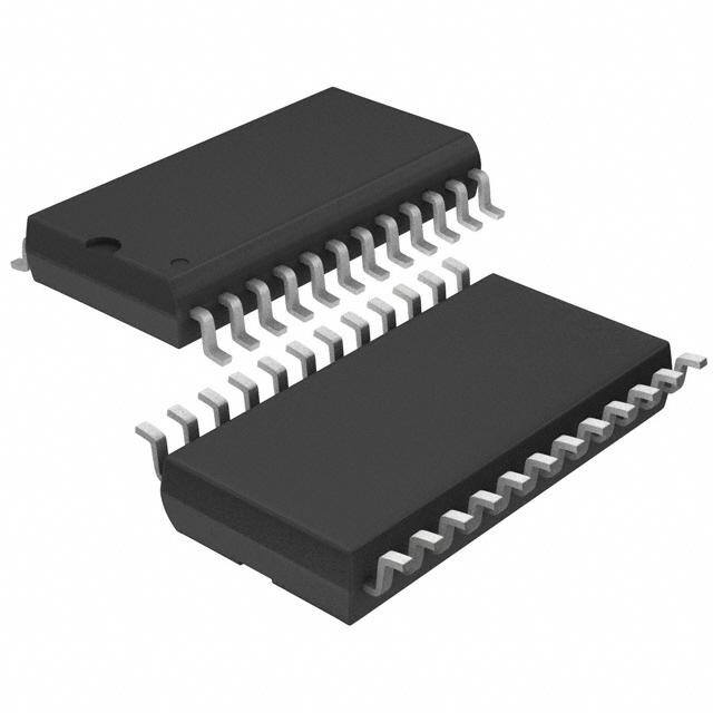
| 描述 | IC A/D CONV 12BIT SAMPLNG 24SOIC |
| 产品分类 | |
| 品牌 | Linear Technology |
| 数据手册 | http://www.linear.com/docs/2239 |
| 产品图片 |
|
| 产品型号 | LTC1272-3ACSW |
| rohs | 含铅 / 不符合限制有害物质指令(RoHS)规范要求 |
| 产品系列 | - |
| 产品目录页面 | |
| 位数 | 12 |
| 供应商器件封装 | 24-SOIC |
| 包装 | 管件 |
| 安装类型 | 表面贴装 |
| 封装/外壳 | 24-SOIC(0.295",7.50mm 宽) |
| 工作温度 | 0°C ~ 70°C |
| 数据接口 | 并联 |
| 标准包装 | 32 |
| 特性 | - |
| 电压源 | 单电源 |
| 转换器数 | 1 |
| 输入数和类型 | 1 个单端,单极 |
| 采样率(每秒) | 250k |


- 商务部:美国ITC正式对集成电路等产品启动337调查
- 曝三星4nm工艺存在良率问题 高通将骁龙8 Gen1或转产台积电
- 太阳诱电将投资9.5亿元在常州建新厂生产MLCC 预计2023年完工
- 英特尔发布欧洲新工厂建设计划 深化IDM 2.0 战略
- 台积电先进制程称霸业界 有大客户加持明年业绩稳了
- 达到5530亿美元!SIA预计今年全球半导体销售额将创下新高
- 英特尔拟将自动驾驶子公司Mobileye上市 估值或超500亿美元
- 三星加码芯片和SET,合并消费电子和移动部门,撤换高东真等 CEO
- 三星电子宣布重大人事变动 还合并消费电子和移动部门
- 海关总署:前11个月进口集成电路产品价值2.52万亿元 增长14.8%


PDF Datasheet 数据手册内容提取
LTC1272 12-Bit, 3µs, 250kHz Sampling A/D Converter FEATURES DESCRIPTION n AD7572 Pinout The LTC1272 is a 3µs, 12-bit, successive approximation n 12-Bit Resolution sampling A/D converter. It has the same pinout as the n 3µs and 8µs Conversion Times industry standard AD7572 and offers faster conversion n On-Chip Sample-and-Hold time, on-chip sample-and-hold, and single supply opera- n Up to 250kHz Sample Rates tion. It uses LTBiCMOS™ switched-capacitor technology n 5V Single Supply Operation to combine a high speed 12-bit ADC with a fast, accurate n No Negative Supply Required sample-and-hold and a precision reference. n On-Chip 25ppm/°C Reference The LTC1272 operates with a single 5V supply but can n 75mW (Typ) Power Consumption also accept the 5V/–15V supplies required by the AD7572 n ESD Protected on All Pins (Pin 23, the negative supply pin of the AD7572, is not con- n 24-Pin Narrow DIP and SOL Packages nected on the LTC1272). The LTC1272 has the same 0V to 5V input range as the AD7572 but, to achieve single supply APPLICATIONS operation, it provides a 2.42V reference output instead of the –5.25V of the AD7572. It plugs in for the AD7572 if the n High Speed Data Acquisition reference capacitor polarity is reversed and a 1µs sample- n Digital Signal Processing (DSP) and-hold acquisition time is allowed between conversions. n Multiplexed Data Acquisition Systems n Single Supply Systems The output data can be read as a 12-bit word or as two 8-bit bytes. This allows easy interface to both 8-bit and L, LT, LTC, LTM, Linear Technology and the Linear logo are registered trademarks and LTBiCMOS is a trademark of Linear Technology Corporation. All other trademarks are the higher processors. The LTC1272 can be used with a crystal property of their respective owners. or an external clock and comes in speed grades of 3ms and 8ms. TYPICAL APPLICATION Single 5V Supply, 3µs, 12-Bit Sampling ADC 1024 Point FFT, f = 250kHz, f = 10kHz S IN LTC1272 5V 0 ANALOG INPUT 2.42V (0V TO 5V) AIN VDD + –20 S VR E F + VREF NC 10µF 0.1µF (N+D)= 72.1 OUTPUT 0.1µF 10µF AGND BUSY –40 B) D11 (MSB) CS µP E (d –60 D D10 RD CONTROL U D9 HBEN LINES PLIT –80 M A D8 CLK OUT –100 D7 CLK IN –120 8 OR 12-BIT D6 D0/8 PARALLEL BUS D5 D1/9 –140 0 20 40 60 80 100 120 D4 D2/10 FREQUENCY (kHz) DGND D3/11 LTC1272 • F02 LTC1272 • F01 1272fc 1 For more information www.linear.com/1272
LTC1272 ABSOLUTE MAXIMUM RATINGS (Notes 1 and 2) Supply Voltage (V ) ..................................................6V Operating Temperature Range DD Analog Input Voltage (Note 3) ....................–0.3V to 15V LTC1272-XAC, CC ....................................0°C to 70°C Digital Input Voltage ...................................–0.3V to 12V Storage Temperature Range ...................–65°C to 150°C Digital Output Voltage .....................–0.3V to V + 0.3V Lead Temperature (Soldering, 10 sec) ..................300°C DD Power Dissipation ...............................................500mW PIN CONFIGURATION TOP VIEW TOP VIEW AIN 1 24 VDD AIN 1 24 VDD VREF 2 23 NC VREF 2 23 NC AGND 3 22 BUSY AGND 3 22 BUSY (MSB) D11 4 21 CS (MSB) D11 4 21 CS D10 5 20 RD D10 5 20 RD D9 6 19 HBEN D9 6 19 HBEN D8 7 18 CLK OUT D8 7 18 CLK OUT D7 8 17 CLK IN D7 8 17 CLK IN D6 9 16 D0/8 D6 9 16 D0/8 D5 10 15 D1/9 D5 10 15 D1/9 D4 11 14 D2/10 D4 11 14 D2/10 DGND 12 13 D3/11 DGND 12 13 D3/11 N PACKAGE SW PACKAGE 24-LEAD PDIP 24-LEAD PLASTIC SO WIDE TJMAX = 110°C, θJA = 100°C/W TJMAX = 110°C, θJA = 130°C/W ORDER INFORMATION LEAD FREE FINISH TAPE AND REEL PART MARKING PACKAGE DESCRIPTION TEMPERATURE RANGE LTC1272ACN-3#PBF LTC1272ACN-3#TRPBF LTC1272-3ACN 24-Lead PDIP 0°C to 70°C LTC1272CCN-3#PBF LTC1272CCN-3#TRPBF LTC1272-3CCN 24-Lead PDIP 0°C to 70°C LTC1272ACN-8#PBF LTC1272ACN-8#TRPBF LTC1272-8ACN 24-Lead PDIP 0°C to 70°C LTC1272CCN-8#PBF LTC1272CCN-8#TRPBF LTC1272-8CCN 24-Lead PDIP 0°C to 70°C LTC1272ACSW-3#PBF LTC1272ACSW-3#TRPBF LTC1272-3ACSW 24-Lead Plastic SO Wide 0°C to 70°C LTC1272CCSW-3#PBF LTC1272CCSW-3#TRPBF LTC1272-3CCSW 24-Lead Plastic SO Wide 0°C to 70°C LTC1272ACSW-8#PBF LTC1272ACSW-8#TRPBF LTC1272-8ACSW 24-Lead Plastic SO Wide 0°C to 70°C LTC1272CCSW-8#PBF LTC1272CCSW-8#TRPBF LTC1272-8CCSW 24-Lead Plastic SO Wide 0°C to 70°C Consult LTC Marketing for parts specified with wider operating temperature ranges. Consult LTC Marketing for information on nonstandard lead based finish parts. For more information on lead free part marking, go to: http://www.linear.com/leadfree/ For more information on tape and reel specifications, go to: http://www.linear.com/tapeandreel/ 1272fc 2 For more information www.linear.com/1272
LTC1272 CONVERTER CHARACTERISTICS The l denotes the specifications which apply over the full operating temperature range, otherwise specifications are at T = 25°C. With Internal Reference (Note 4) A LTC1272-XA LTC1272-XC PARAMETER CONDITIONS MIN TYP MAX MIN TYP MAX UNITS Resolution (No Missing Codes) l 12 12 Bits Integral Linearity Error (Note 5) l ±1/2 ±1 LSB Differential Linearity Error l ±1 ±1 LSB Offset Error ±3 ±4 LSB l ±4 ±6 LSB Gain Error ±10 ±15 LSB Full-Scale Tempco I (Reference) = 0 l ±5 ±25 ±10 ±45 ppm/°C OUT INTERNAL REFERENCE CHARACTERISTICS The l denotes the specifications which apply over the full operating temperature range, otherwise specifications are at T = 25°C. (Note 4) A LTC1272-XA LTC1272-XC PARAMETER CONDITIONS MIN TYP MAX MIN TYP MAX UNITS V Output Voltage (Note 6) I = 0 2.400 2.420 2.440 2.400 2.420 2.440 V REF OUT V Output Tempco I = 0 l 5 25 10 45 ppm/°C REF OUT V Line Regulation 4.75V ≤ V ≤ 5.25V, I = 0 0.01 0.01 LSB/V REF DD OUT VREF Load Regulation (Sourcing Current) 0 ≤ IOUT ≤ 1mA 2 2 LSB/mA DIGITAL AND DC ELECTRICAL CHARACTERISTICS The l denotes the specifications which apply over the full operating temperature range, otherwise specifications are at T = 25°C. (Note 4) A LTC1272-XA/C SYMBOL PARAMETER CONDITIONS MIN TYP MAX UNITS V High Level Input Voltage CS, RD, HBEN, CLK IN V = 5.25V l 2.4 V IH DD V Low Level Input Voltage CS, RD, HBEN, CLK IN V = 4.75V l 0.8 V IL DD I Input Current CS, RD, HBEN V = 0V to V l ±10 µA IN IN DD Input Current CLK IN V = 0V to V l ±20 µA IN DD V High Level Output Voltage All Logic Outputs V = 4.75V I = –10μA 4.7 V OH DD OUT I = –200μA l 4.0 V OUT V Low Level Output Voltage All Logic Outputs V = 4.75V, I = 1.6mA l 0.4 V OL DD OUT I High-Z Output Leakage D11-D0/8 V = 0V to V l ±10 µA OZ OUT DD C High-Z Output Capacitance (Note 7) l 15 pF OZ I Output Source Current V = 0V –10 mA SOURCE OUT I Output Sink Current V = V 10 mA SINK OUT DD I Positive Supply Current CS = RD = V , A = 5V l 15 30 mA DD DD IN P Power Dissipation 75 mW D 1272fc 3 For more information www.linear.com/1272
LTC1272 DYNAMIC ACCURACY (Note 4) f = 250kHz (LTC1272-3), 111kHz (LTC1272-8) SAMPLE LTC1272-XA/C SYMBOL PARAMETER CONDITIONS MIN TYP MAX UNITS S/(N+D) Signal-to-Noise Plus Distortion Ratio 10kHz Input Signal 72 dB THD Total Harmonic Distortion (Up to 5th Harmonic) 10kHz Input Signal –82 dB Peak Harmonic or Spurious Noise 10kHz Input Signal –82 dB ANALOG INPUT The l denotes the specifications which apply over the full operating temperature range, otherwise specifications are at T = 25°C. (Note 4) A LTC1272-XA/B/C SYMBOL PARAMETER CONDITIONS MIN TYP MAX UNITS V Input Voltage Range 4.75V ≤ V ≤ 5.25V l 0 5 V IN DD I Input Current l 3.5 mA IN C Input Capacitance 50 pF IN t Sample-and-Hold Acquisition Time l 0.45 1 µs ACQ TIMING CHARACTERISTICS The l denotes the specifications which apply over the full operating temperature range, otherwise specifications are at T = 25°C. (Note 8) A LTC1272-XA/C SYMBOL PARAMETER CONDITIONS MIN TYP MAX UNITS t CS to RD Setup Time l 0 ns 1 t RD to BUSY Delay C = 50pF 80 190 ns 2 L COM Grade l 230 ns t3 Data Access Time After RD↓ CL = 20pF 50 90 ns COM Grade l 110 ns C = 100pF 70 125 ns L COM Grade l 150 ns t RD Pulse Width t ns 4 3 COM Grade l t ns 3 t CS to RD Hold Time l 0 ns 5 t Data Setup Time After BUSY 40 70 ns 6 COM Grade l 90 ns t Bus Relinquish Time 20 30 75 ns 7 COM Grade l 20 85 ns t HBEN to RD Setup Time l 0 ns 8 t HBEN to RD Hold Time l 0 ns 9 t Delay Between RD Operations l 200 ns 10 t Delay Between Conversions 1 µs 11 t Aperture Delay of Sample and Hold Jitter <50ps 25 ns 12 t CLK to BUSY Delay 80 170 ns 13 COM Grade l 220 ns t Conversion Time l 12 13 CLK CONV CYCLES 1272fc 4 For more information www.linear.com/1272
LTC1272 ELECTRICAL CHARACTERISTICS Note 1: Stresses beyond those listed under Absolute Maximum Ratings Note 5: Linearity error is specified between the actual end points of the may cause permanent damage to the device. Exposure to any Absolute A/D transfer curve. Maximum Rating condition for extended periods may affect device Note 6: The LTC1272 has the same 0V to 5V input range as the AD7572 reliability and lifetime. but, to achieve single supply operation, it provides a 2.42V reference Note 2: All voltage values are with respect to ground with DGND and output instead of the –5.25V of the AD7572. This requires that the polarity AGND wired together, unless otherwise noted. of the reference bypass capacitor be reversed when plugging an LTC1272 Note 3: When the analog input voltage is taken below ground it will be into an AD7572 socket. clamped by an internal diode. This product can handle, with no external Note 7: Guaranteed by design, not subject to test. diode, input currents of greater than 60mA below ground without latch-up. Note 8: VDD = 5V. Timing specifications are sample tested at 25°C to Note 4: V = 5V, f = 4MHz for LTC1272-3, and 1.6MHz for ensure compliance. All input control signals are specified with t = t = 5ns DD CLK r f LTC1272-8, t = t = 5ns unless otherwise specified. For best analog (10% to 90% of 5V) and timed from a voltage level of 1.6V. See Figures 13 r f performance, the LTC1272 clock should be synchronized to the RD and through 17. CS control inputs with at least 40ns separating convert start from the nearest clock edge. 1272fc 5 For more information www.linear.com/1272
LTC1272 PIN FUNCTIONS A (Pin 1): Analog Input, 0V to 5V Unipolar Input. HBEN (Pin 19): High Byte Enable Input. This pin is used IN to multiplex the internal 12-bit conversion result into the V (Pin 2): 2.42V Reference Output. When plugging into REF lower bit outputs (D7 to D0/8). See table below. HBEN an AD7572 socket, reverse the reference bypass capacitor also disables conversion starts when HIGH. polarity and short the 10Ω series resistor. RD (Pin 20): Read Input. This active low signal starts a AGND (Pin 3): Analog Ground. conversion when CS and HBEN are low. RD also enables D11 to D4 (Pins 4-11): Three-State Data Outputs. the output drivers when CS is low. DGND (Pin 12): Digital Ground. CS (Pin 21): The Chip Select Input must be low for the ADC to recognize RD and HBEN inputs. D3/11 to D0/8 (Pins 13-16): Three-State Data Outputs. BUSY (Pin 22): The BUSY Output is low when a conver- CLK IN (Pin 17): Clock Input. An external TTL/CMOS sion is in progress. compatible clock may be applied to this pin or a crystal can be connected between CLK IN and CLK OUT. NC (Pin 23): Not Connected Internally. The LTC1272 does not require negative supply. This pin can accommodate CLK OUT (Pin 18): Clock Output. An inverted CLK IN signal the –15V required by the AD7572 without problems. appears at this pin. V (Pin 24): Positive Supply, 5V. DD Data Bus Output, CS and RD = LOW Pin 4 Pin 5 Pin 6 Pin 7 Pin 8 Pin 9 Pin 10 Pin 11 Pin 13 Pin 14 Pin 15 Pin 16 MNEMONIC* D11 D10 D9 D8 D7 D6 D5 D4 D3/11 D2/10 D1/9 D0/8 HBEN = LOW DB11 DB10 DB9 DB8 DB7 DB6 DB5 DB4 DB3 DB2 DB1 DB0 HBEN = HIGH DB11 DB10 DB9 DB8 LOW LOW LOW LOW DB11 DB10 DB9 DB8 * D11...D0/8 are the ADC data output pins. DB11...DB0 are the 12-bit conversion results, DB11 is the MSB. TYPICAL PERFORMANCE CHARACTERISTICS Integral Nonlinearity 1.0 VDD = 5V fCLK = 4MHz 0.5 s) B S L R ( O 0 R R E L N I –0.5 –1.0 00 512 1024 1536 2048 2560 3072 3584 4096 CODE LTC1272 • G01 1272fc 6 For more information www.linear.com/1272
LTC1272 TYPICAL PERFORMANCE CHARACTERISTICS Differential Nonlinearity 1.0 VDD = 5V fCLK = 4MHz 0.5 s) B S L R ( O 0 R R E L N I –0.5 –1.0 00 512 1024 1536 2048 2560 3072 3584 4096 CODE LTC1272 • G02 V Supply Current vs Minimum Clock Frequency vs Maximum Clock Frequency vs DD Temperature Temperature Temperature 30 600 8 VDD = 5V VDD = 5V A) 25 fCLK = 4MHz 500 7 m (D Hz) Hz) ENT, ID 20 NCY (k400 NCY (M 6 URR 15 QUE300 QUE 5 UPPLY C 10 OCK FRE200 OCK FRE 4 SD CL CL VD 5 100 3 0 0 2 –55 –25 0 25 50 75 100 125 –55 –25 0 25 50 75 100 125 –55 –25 0 25 50 75 100 125 TEMPERATURE (°C) TEMPERATURE (°C) TEMPERATURE (°C) LT1272 • G03 LT1272 • G04 LT1272 • G05 V vs I (mA) LTC1272 ENOBs* vs Frequency REF LOAD 2.435 12 11 2.430 10 9 2.425 8 (V)REF2.420 NOBs* 67 V E 5 2.415 4 3 2.410 2 1 VfSD =D 2=5 50VkHz 2.405 0 –5 –4 –3 –2 –1 0 1 2 0 20 40 60 80 100 120 IL (mA) fIN (kHz) LT1272 • G06 S/(N + D) – 1.76dB *EFFECTIVE NUMBER OF BITS, ENOBs = 6.02 LT1272 • G07 1272fc 7 For more information www.linear.com/1272
LTC1272 APPLICATIONS INFORMATION Conversion Details AIN SAMPLE Conversion start is controlled by the CS, RD and HBEN inputs. At the start of conversion the successive approxi- 300Ω SI SAMPLE CSAMPLE mation register (SAR) is reset and the three-state data – outputs are enabled. Once a conversion cycle has begun HOLD it cannot be restarted. 2.7k + COMPARATOR During conversion, the internal 12-bit capacitive DAC CDAC DAC output is sequenced by the SAR from the most significant VDAC S bit (MSB) to the least significant bit (LSB). Referring to A R Figure 1, the A input connects to the sample-and-hold IN capacitor through a 300Ω/2.7k divider. The voltage divider 12-BIT allows the LTC1272 to convert 0V to 5V input signals LATCH while operating from a 4.5V supply. The conversion has LTC1272 • F01 Figure 1. A Input two phases: the sample phase and the convert phase. IN During the sample phase, the comparator offset is nulled by the feedback switch and the analog input is stored earity and differential nonlinearity. These specs are useful as a charge on the sample-and-hold capacitor, C . for characterizing an ADC’s DC or low frequency signal SAMPLE This phase lasts from the end of the previous conversion performance. until the next conversion is started. A minimum delay These specs alone are not adequate to fully specify the between conversions (t ) of 1µs allows enough time 10 LTC1272 because of its high speed sampling ability. FFT for the analog input to be acquired. During the convert (Fast Fourrier Transform) test techniques are used to phase, the comparator feedback switch opens, putting characterize the LTC1272’s frequency response, distortion the comparator into the compare mode. The sample-and- and noise at the rated throughput. hold capacitor is switched to ground injecting the analog input charge onto the comparator summing junction. This By applying a low distortion sine wave and analyzing the input charge is successively compared to binary weighted digital output using a FFT algorithm, the LTC1272’s spectral charges supplied by the capacitive DAC. Bit decisions are content can be examined for frequencies outside the fun- made by the comparator (zero crossing detector) which damental. Figure 2 shows a typical LTC1272 FFT plot. checks the addition of each successive weighted bit from 0 the DAC output. The MSB decision is made 50ns (typi- –10 cally) after the second falling edge of CLK IN following a –20 conversion start. Similarly, the succeeding bit decisions –30 are made approximately 50ns after a CLK IN edge until dB)–40 the conversion is finished. At the end of a conversion, DE (–50 U the DAC output balances the AIN output charge. The SAR MPLIT––7600 contents (12-bit data word) which represent the A input A IN –80 signal are loaded into a 12-bit latch. –90 –100 Sample-and-Hold and Dynamic Performance –110 0 20 40 60 80 100 120 Traditionally A/D converters have been characterized by FREQUENCY (kHz) LTC1272 • F02 such specs as offset and full-scale errors, integral nonlin- Figure 2. LTC1272 Non-Averaged, 1024 Point FFT Plot. f = 250kHz, f = 10kHz S IN 1272fc 8 For more information www.linear.com/1272
LTC1272 APPLICATIONS INFORMATION Signal-to-Noise Ratio 1.0 The Signal-to-Noise Ratio (SNR) is the ratio between the RMS amplitude of the fundamental input frequency to 0.5 the RMS amplitude of all other frequency components at B) the A/D output. This includes distortion as well as noise LS R ( 0 products and for this reason it is sometimes referred to as O R R Signal-to-Noise + Distortion [S/(N + D)]. The output is band E limited to frequencies from DC to one half the sampling –0.5 frequency. Figure 2 shows spectral content from DC to 125kHz which is 1/2 the 250kHz sampling rate. –1.0 00 1 2 3 4 Effective Number of Bits CODE (THOUSANDS) LTC1272 • F04 The effective number of bits (ENOBs) is a measurement Figure 4. LTC1272 Dynamic DNL. f = 4MHz, CLK of the resolution of an A/D and is directly related to the f = 250kHz, f = 122.25342kHz, V = 5V S IN CC S/(N + D) by the equation: N = [S/(N + D) –1.76]/6.02 Total Harmonic Distortion where N is the effective number of bits of resolution and Total Harmonic Distortion (THD) is the ratio of the RMS S/(N + D) is expressed in dB. At the maximum sampling sum of all harmonics of the input signal to the fundamental rate of 250kHz the LTC1272 maintains 11.5 ENOBs or bet- itself. The harmonics are limited to the frequency band ter to 20kHz. Above 20kHz the ENOBs gradually decline, between DC and one half the sampling frequency. THD is as shown in Figure 3, due to increasing second harmonic expressed as: 20 LOG [√V 2 + V 2 + ... + V 2 /V ] where 2 3 N 1 distortion. The noise floor remains approximately 90dB. V is the RMS amplitude of the fundamental frequency and 1 The dynamic differential nonlinearity remains good out to V through V are the amplitudes of the second through 2 N 120kHz as shown in Figure 4. Nth harmonics. Clock and Control Synchronization 12 For best analog performance, the LTC1272 clock should be 11 synchronized to the CS and RD control inputs as shown in 10 Figure 5, with at least 40ns separating convert start from 9 8 the nearest CLK IN edge. This ensures that transitions at * 7 CLK IN and CLK OUT do not couple to the analog input s NOB 6 and get sampled by the sample-and-hold. The magnitude E 5 of this feedthrough is only a few millivolts, but if CLK and 4 3 convert start (CS and RD) are asynchronous, frequency 2 components caused by mixing the clock and convert 1 VfSD =D 2=5 50VkHz signals may increase the apparent input noise. 0 0 20 40 60 80 100 120 When the clock and convert signals are synchronized, fIN (kHz) LT1272 • F03 small endpoint errors (offset and full-scale) are the most that can be generated by clock feedthrough. Even these Figure 3. LTC1272 Effective Number of Bits (ENOBs) vs Input errors (which can be trimmed out) can be eliminated Frequency. f = 250kHz S by ensuring that the start of a conversion (CS and RD’s falling edge) does not occur within 40ns of a clock edge, 1272fc 9 For more information www.linear.com/1272
LTC1272 APPLICATIONS INFORMATION CS & RD t2 tCONV BUSY ≥ 40ns* t13 CLK IN t14 DB11 DB10 DB1 DB0 (MSB) (LSB) UNCERTAIN CONVERSION TIME FOR 30ns < t14 < 180ns *THE LTC1272 IS ALSO COMPATIBLE WITH THE AD7572 SYNCHRONIZATION MODES. LTC1272 • F05 Figure 5. RD and CLK IN for Synchronous Operation as in Figure 5. Nevertheless, even without observing this CLK OUT guideline, the LTC1272 is still compatible with AD7572 C1 LTC1272 18 synchronization modes, with no increase in linearity error. C2 This means that either the falling or rising edge of CLK IN 17 CLOCK may be near RD’s falling edge. CLK IN 1M Driving the Analog Input NOTES: LTC1272-3 – 4MHz CRYSTAL/CERAMIC RESONATOR The analog input of the LTC1272 is much easier to drive LTC1272-8 – 1.6MHz CRYSTAL/CERAMIC RESONATOR LTC1272 • F06 than that of the AD7572. The input current is not modulated Figure 6. LTC1272 Internal Clock Circuit by the DAC as in the AD7572. It has only one small current spike from charging the sample-and-hold capacitor at the to CLK IN. For an external clock the duty cycle is not end of the conversion. During the conversion the analog critical. An inverted CLK IN signal will appear at the CLK input draws only DC current. The only requirement is that OUT pin as shown in the operating waveforms of Figure 7. the amplifier driving the analog input must settle after the Capacitance on the CLK OUT pin should be minimized for small current spike before the next conversion is started. best analog performance. Any op amp that settles in 1µs to small current transients will allow maximum speed operation. If slower op amps Internal Reference are used, more settling time can be provided by increasing the time between conversions. Suitable devices capable The LTC1272 has an on-chip, temperature compensated, of driving the LTC1272 A input include the LT1006 and curvature corrected, bandgap reference, which is factory IN LT1007 op amps. trimmed to 2.42V ±1%. It is internally connected to the DAC and is also available at pin 2 to provide up to 1mA Internal Clock Oscillator current to an external load. Figure 6 shows the LTC1272 internal clock circuit. A crystal For minimum code transition noise the reference output or ceramic resonator may be connected between CLK IN should be decoupled with a capacitor to filter wideband (Pin 17) and CLK OUT (Pin 18) to provide a clock oscillator noise from the reference (10µF tantalum in parallel with for ADC timing. Alternatively the crystal/resonator may be a 0.1µF ceramic). A simplified schematic of the reference omitted and an external clock source may be connected with its recommended decoupling is shown in Figure 8. 1272fc 10 For more information www.linear.com/1272
LTC1272 APPLICATIONS INFORMATION CS & RD BUSY 50ns TYP CLK IN CLK OUT DB11 DB10 DB1 DB0 (MSB) (LSB) LTC1272 • F07 Figure 7. Operating Waveforms Using an External Clock Source for CLK IN FULL-SCALE 11...111 5V TRANSITION LTC1272 11...110 + CURVATURE 11...101 CORRECTED TO DAC E BANDGAP D O REFERENCE – C T U FS = 5V P T FS U 1LSB =–––– O 4096 AGND VREF 00...011 3 2 00...010 0.1µF 00...001 00...000 0 1 2 3 FS LSB LSBs FS – 1LSB 10µF LSBs + LTC1272 • F08 AIN, INPUT VOLTAGE (IN TERMS OF LSBs) LT1272 • F09 Figure 8. LTC1272 Internal 2.42V Reference Figure 9. LTC1272 Ideal Input/Output Transfer Characteristic Unipolar Operation error must be adjusted before full-scale error. Figure 10 shows the extra components required for full-scale error Figure 9 shows the ideal input/output characteristic for the adjustment. Zero offset is achieved by adjusting the offset 0V to 5V input range of the LTC1272. The code transitions of the op amp driving A (i.e., A1 in Figure 10). For zero occur midway between successive integer LSB values IN offset error apply 0.61mV (i.e., 1/2LBS) at V and adjust (i.e., 1/2LSB, 3/2LSBs, 5/2LSBs . . . FS – 3/2LSBs). The IN the op amp offset voltage until the ADC output code flickers output code is natural binary with 1 LSB = FS/4096 = between 0000 0000 0000 and 0000 0000 0001. (5/4096)V = 1.22mV. For zero full-scale error apply an analog input of 4.99817V Unipolar Offset and Full-Scale Error Adjustment (i.e., FS – 3/2LSBs or last code transition) at V and adjust IN R1 until the ADC output code flickers between 1111 1111 In applications where absolute accuracy is important, then 1110 and 1111 1111 1111. offset and full-scale error can be adjusted to zero. Offset 1272fc 11 For more information www.linear.com/1272
LTC1272 APPLICATIONS INFORMATION sential to low noise operation of the ADC and the foil width 0AVN TAOL O5GV VIN + R3 for these tracks should be as wide as possible. INPUT A1 15Ω LT1007 1 AIN Noise: Input signal leads to AIN and signal return leads – from AGND (pin 3) should be kept as short as possible to LTC1272 minimize input noise coupling. In applications where this R1 200Ω R2 is not possible, a shielded cable between source and ADC 20k 3 AGND is recommended. Also, since any potential difference in *ADDITIONAL PINS OMITTED FOR CLARITY grounds between the signal source and ADC appears as LTC1272 • F10 an error voltage in series with the input signal, attention should be paid to reducing the ground circuit impedances Figure 10. Unipolar 0V to 5V Operation with Gain Error Adjust as much as possible. In applications where the LTC1272 data outputs and Application Hints control signals are connected to a continuously active Wire wrap boards are not recommended for high reso- microprocessor bus, it is possible to get LSB errors in lution or high speed A/D converters. To obtain the best conversion results. These errors are due to feedthrough performance from the LTC1272 a printed circuit board is from the microprocessor to the successive approximation required. Layout for the printed circuit board should en- comparator. The problem can be eliminated by forcing the sure that digital and analog signal lines are separated as microprocessor into a Wait state during conversion (see much as possible. In particular, care should be taken not Slow Memory Mode interfacing), or by using three-state to run any digital track alongside an analog signal track buffers to isolate the LTC1272 data bus. or underneath the LTC1272. The analog input should be screened by AGND. Timing and Control A single point analog ground separate from the logic system Conversion start and data read operations are controlled by ground should be established with an analog ground plane three LTC1272 digital inputs; HBEN, CS and RD. Figure 12 at pin 3 (AGND) or as close as possible to the LTC1272, shows the logic structure associated with these inputs. as shown in Figure 11. Pin 12 (LTC1272 DGND) and all The three signals are internally gated so that a logic “0” is other analog grounds should be connected to this single required on all three inputs to initiate a conversion. Once analog ground point. No other digital grounds should be initiated it cannot be restarted until conversion is complete. connected to this analog ground point. Low impedance Converter status is indicated by the BUSY output, and this analog and digital power supply common returns are es- is low while conversion is in progress. 1 LTC1272 DIGITAL AIN SYSTEM ANALOG + AGND VREF VDD DGND INPUT 3 2 24 12 CIRCUITRY – C1 C2 C3 C4 GROUND CONNECTION TO DIGITAL CIRCUITRY ANALOG GROUND PLANE LTC1272 • F11 Figure 11. Power Supply Grounding Practice 1272fc 12 For more information www.linear.com/1272
LTC1272 APPLICATIONS INFORMATION There are two modes of operation as outlined by the tim- The second is the ROM Mode which does not require ing diagrams of Figures 13 to 17. Slow Memory Mode is microprocessor Wait states. A Read operation brings CS designed for microprocessors which can be driven into a and RD low which initiates a conversion and reads the Wait state, a Read operation brings CS and RD low which previous conversion result. initiates a conversion and data is read when conversion is complete. 5V LTC1272 HBEN 19 D Q CONVERSION START (RISING EDGE TRIGGER) CS 21 FLIP FLOP RD 20 CLEAR BUSY ACTIVE HIGH ENABLE THREE-STATE OUTPUTS D11....D0/8 = DB11....DB0 ACTIVE HIGH ENABLE THREE-STATE OUTPUTS D11....D8 = DB11....DB8 D7....D4 = LOW D3/11....D0/8 = DB11....DB8 D11....D0/8 ARE THE ADC DATA OUTPUT PINS DB11....DB0 ARE THE 12-BIT CONVERSION RESULTS LTC1272 • F12 Figure 12. Internal Logic for Control Inputs CS, RD and HBEN CS & RD t2 tCONV BUSY ≥ 40ns* t13 CLK IN t14 DB11 DB10 DB1 DB0 (MSB) (LSB) UNCERTAIN CONVERSION TIME FOR 30ns < t14 < 180ns *THE LTC1272 IS ALSO COMPATIBLE WITH THE AD7572 SYNCHRONIZATION MODES. LTC1272 • F13 SEE “DIGITAL INTERFACE” TEXT. Figure 13. RD and CLK IN for Synchronous Operation Table 1. Data Bus Output, CS and RD = Low PIN 4 PIN 5 PIN 6 PIN 7 PIN 8 PIN 9 PIN 10 PIN 11 PIN 13 PIN 14 PIN 15 PIN 16 Data Outputs* D11 D10 D9 D8 D7 D6 D5 D4 D3/11 D2/10 D1/9 D0/8 HBEN = LOW DB11 DB10 DB9 DB8 DB7 DB6 DB5 DB4 DB3 DB2 DB1 DB0 HBEN = HIGH DB11 DB10 DB9 DB8 LOW LOW LOW LOW DB11 DB10 DB9 DB8 Note: *D11 . . . D0/8 are the ADC data output pins DB11 . . . DB0 are the 12-bit conversion results, DB11 is the MSB 1272fc 13 For more information www.linear.com/1272
LTC1272 APPLICATIONS INFORMATION CS t1 t5 t1 RRDD t10 t2 t11 tCONV BUSY t3 t6 t7 OLD DATA NEW DATA DATA DB11-DB0 DB11-DB0 t12 HOLD TRACK LTC1272 • F14 Figure 14. Slow Memory Mode, Parallel Read Timing Diagram Table 2. Slow Memory Mode, Parallel Read Data Bus Status Data Outputs D11 D10 D9 D8 D7 D6 D5 D4 D3/11 D2/10 D1/9 D0/8 Read DB11 DB10 DB9 DB8 DB7 DB6 DB5 DB4 DB3 DB2 DB1 DB0 Data Format Slow Memory Mode, Two Byte Read The output data format can be either a complete parallel For a two byte read, only 8 data outputs D7 . . . D0/8 are load for 16-bit microprocessors or a two byte load for used. Conversion start procedure and data output status 8-bit microprocessors. Data is always right justified (i.e., for the first read operation is identical to Slow Memory LSB is the most right-hand bit in a 16-bit word). For a two Mode, Parallel Read. See Figure 15 timing diagram and byte read, only data outputs D7. . . D0/8 are used. Byte Table 3 data bus status. At the end of conversion the low selection is governed by the HBEN input which controls data byte (DB7 . . . DB0) is read from the ADC. A second an internal digital multiplexer. This multiplexes the 12 bits Read operation with HBEN high, places the high byte on of conversion data onto the lower D7. . .D0/8 outputs data outputs D3/11 . . . D0/8 and disables conversion (4MSBs or 8LSBs) where it can be read in two read cycles. start. Note the 4MSBs appear on data outputs D11 . . . The 4MSBs always appear on D11 . . . D8 whenever the D8 during the two Read operations above. three-state output drives are turned on. ROM Mode, Parallel Read (HBEN = Low) Slow Memory Mode, Parallel Read (HBEN = Low) The ROM Mode avoids placing a microprocessor into a Figure 14 and Table 2 show the timing diagram and data Wait state. A conversion is started with a Read operation bus status for Slow Memory Mode, Parallel Read. CS and the 12 bits of data from the previous conversion is and RD going low triggers a conversion and the LTC1272 available on data outputs D11 . . . D0/8 (see Figure 16 and acknowledges by taking BUSY low. Data from the previous Table 4). This data may be disregarded if not required. A conversion appears on the three-state data outputs. BUSY second Read operation reads the new data (DB11 . . . DB0) returns high at the end of conversion when the output and starts another conversion. A delay at least as long latches have been updated and the conversion result is as the LTC1272 conversion time plus the 1µs minimum placed on data outputs D11 . . . D0/8. delay between conversions must be allowed between Read operations. 1272fc 14 For more information www.linear.com/1272
LTC1272 APPLICATIONS INFORMATION HBEN t8 t9 t8 t9 CS t1 t5 t1 t4 t5 RRDD t10 t10 t2 tCONV t11 BUSY t3 t6 t7 t3 t7 OLD DATA NEW DATA NEW DATA DATA DB7-DB0 DB7-DB0 DB11-DB8 t12 t12 HOLD TRACK LTC1272 • F15 Figure 15. Slow Memory Mode, Two Byte Read Timing Diagram Table 3. Slow Memory Mode, Two Byte Read Data Bus Status Data Outputs D7 D6 D5 D4 D3/11 D2/10 D1/9 D0/8 First Read DB7 DB6 DB5 DB4 DB3 DB2 DB1 DB0 Second Read Low Low Low Low DB11 DB10 DB9 DB8 CS t1 t4 t5 t1 t4 t5 RD t11 t2 tCONV t2 tCONV BUSY t3 t7 t3 t7 OLD DATA NEW DATA DATA DB11-DB0 DB11-DB0 t12 t12 HOLD TRACK LTC1272 • F16 Figure 16. ROM Mode, Parallel Read Timing Diagram Table 4. ROM Mode, Parallel Read Data Bus Status Data Outputs D11 D10 D9 D8 D7 D6 D5 D4 D3/11 D2/10 D1/9 D0/8 First Read (Old Data) DB11 DB10 DB9 DB8 DB7 DB6 DB5 DB4 DB3 DB2 DB1 DB0 Second Read DB11 DB10 DB9 DB8 DB7 DB6 DB5 DB4 DB3 DB2 DB1 DB0 1272fc 15 For more information www.linear.com/1272
LTC1272 APPLICATIONS INFORMATION HBEN t8 t9 t8 t9 t8 t9 CS t1 t4 t5 t1 t4 t5 t1 t4 t5 RRDD t10 t2 tCONV t11 t2 BUSY t3 t7 t3 t7 t3 t7 OLD DATA NEW DATA NEW DATA DATA DB7-DB0 DB11-DB8 DB7-DB0 t12 t12 HOLD TRACK LTC1272 • F17 Figure 17. ROM Mode, Two Byte Read Timing Diagram Table 5. ROM Mode, Two Byte Read Data Bus Status Data Outputs D7 D6 D5 D4 D3/11 D2/10 D1/9 D0/8 First Read DB7 DB6 DB5 DB4 DB3 DB2 DB1 DB0 Second Read Low Low Low Low DB11 DB10 DB9 DB8 Third Read DB7 DB6 DB5 DB4 DB3 DB2 DB1 DB0 ROM Mode, Two Byte READ Microprocessor Interfacing As previously mentioned for a two byte read, only data The LTC1272 is designed to interface with microproces- outputs D7 . . . D0/8 are used. Conversion is started in sors as a memory mapped device. The CS and RD control the normal way with a Read operation and the data output inputs are common to all peripheral memory interfacing. status is the same as the ROM Mode, Parallel Read. See The HBEN input serves as a data byte select for 8-bit pro- Figure 17 timing diagram and Table 5 data bus status. cessors and is normally connected to the microprocessor Two more Read operations are required to access the new address bus. conversion result. A delay equal to the LTC1272 conversion time must be allowed between conversion start and the MC68000 Microprocessor second data Read operation. The second Read operation, Figure 18 shows a typical interface for the MC68000. The with HBEN high, disables conversion start and places the LTC1272 is operating in the Slow Memory Mode. Assuming high byte (4 MSBs) on data outputs D3/11 . . . DO18. A the LTC1272 is located at address C000, then the following third read operation accesses the low data byte (DB7 single 16-bit Move instruction both starts a conversion . . . DB0) and starts another conversion. The 4 MSB’s and reads the conversion result: appear on data outputs D11 . . . D8 during all three read Move.W $C000,D0 operations above. 1272fc 16 For more information www.linear.com/1272
LTC1272 APPLICATIONS INFORMATION is accomplished with the single 16-bit Load instruction A23 A1 ADDRESS BUS below: For the 8085A LHLD (B000) ADDRESS AS EN DECODE For the Z80 LDHL, (B000) MC68000 LTC1272 CS This is a two byte read instruction which loads the ADC data DTACK BUSY (address B000) into the HL register pair. During the first R/W RD read operation, BUSY forces the microprocessor to Wait D11 D11 DATA BUS for the LTC1272 conversion. No Wait states are inserted D0 D0/8 HBEN during the second read operation when the microprocessor is reading the high data byte. ADDITIONAL PINS OMITTED FOR CLARITY LTC1272 • F18 Figure 18. LTC1272 MC68000 Interface TMS32010 Microcomputer At the beginning of the instruction cycle when the ADC Figure 20 shows an LTC1272 TMS32010 interface. The address is selected, BUSY and CS assert DTACK, so that LTC1272 is operating in the ROM Mode. The interface is the MC68000 is forced into a Wait state. At the end of designed for a maximum TMS32010 clock frequency of conversion BUSY returns high and the conversion result 18MHz but will typically work over the full TMS32010 is placed in the D0 register of the microprocessor. clock frequency range. 8085A, Z80 Microprocessor The LTC1272 is mapped at a port address. The following I/O instruction starts a conversion and reads the previous Figure 19 shows a LTC1272 interface for the Z80 and conversion result into data memory: 8085A. The LTC1272 is operating in the Slow Memory Mode and a two byte read is required. Not shown in the IN A,PA (PA = PORT ADDRESS) figure is the 8-bit latch required to demultiplex the 8085A common address/data bus. A0 is used to assert HBEN, When conversion is complete, a second I/O instruction so that an even address (HBEN = LOW) to the LTC1272 reads the up-to-date data into memory and starts another will start a conversion and read the low data byte. An odd conversion. A delay at least as long as the ADC conversion address (HBEN = HIGH) will read the high data byte. This time must be allowed between I/O instructions. A15 PA2 ADDRESS BUS A0 PORT ADDRESS BUS A0 PA0 ADDRESS ADDRESS MREQ EN DECODE DEN EN DECODE Z80 HBEN TMS32010 LTC1272 8085A CS CS WAIT BUSY LTC1272 RD RD RD D7 D7 D11 D11 DATA BUS DATA BUS D0 D0/8 D0 D0/8 HBEN LINEAR CIRCUITRY OMITTED FOR CLARITY LINEAR CIRCUITRY OMITTED FOR CLARITY LTC1272 • F19 LTC1272 • F20 Figure 19. LTC1272 8085A/Z80 Interface Figure 20. LTC1272 TMS32010 Interface 1272fc 17 For more information www.linear.com/1272
LTC1272 APPLICATIONS INFORMATION Compatibility with the AD7572 time between conversions must be provided to allow the sample-and-hold to reacquire the analog input. Figure 22 Figure 21 shows the simple, single 5V configuration shows that if the clock is synchronous with CS and RD, recommended for new designs with the LTC1272. If an it is only necessary to short out the 10Ω series resistor AD7572 replacement or upgrade is desired, the LTC1272 and reverse the polarity of the 10µF bypass capacitor on can be plugged into an AD7572 socket with minor modi- the V pin. The –15V supply is not required and can be fications. It can be used as a replacement or to upgrade REF removed, or, because there is no internal connection to with sample-and-hold, single supply operation and reduced pin 23, it can remain unmodified. The clock can be con- power consumption. sidered synchronous with CS and RD in cases where the The LTC1272, while consuming less power overall than the LTC1272 CLK IN signal is derived from the same clock as AD7572, draws more current from the 5V supply (it draws the microprocessor reading the LTC1272. no power from the –15V supply). Also, a 1µs minimum LTC1272 5V ANALOG INPUT 2.42V (0V TO 5V) AIN VDD + VR E F + VREF NC 10µF 0.1µF* OUTPUT 0.1µF 10µF AGND BUSY D11 (MSB) CS µP D10 RD CONTROL LINES D9 HBEN D8 CLK OUT D7 CLK IN 8 OR 12-BIT D6 D0/8 PARALLEL BUS D5 D1/9 D4 D2/10 * DGND D3/11 LTC1272 • 21 *FOR GROUNDING AND BYPASSING HINTS SEE FIGURE 11 AND APPLICATION HINTS SECTION Figure 21. Single 5V Supply, 3µs, 12-Bit Sampling ADC 1272fc 18 For more information www.linear.com/1272
LTC1272 APPLICATIONS INFORMATION LTC1272 ANALOG INPUT 2.42V* (0V TO 5V) 10Ω* AIN VDD + 5V VR E F + VREF NC(cid:31) –15V 0.1µF 10µF OUTPUT 10µF 0.1µF AGND BUSY 0.1µF 10µF + D11 (MSB) CS µP † D10 RD CONTROL LINES D9 HBEN D8 CLK OUT D7 CLK IN** µP D6 D0/8 DATA *THE LTC1272 HAS THE SAME 0V TO 5V INPUT RANGE BUT PROVIDES A 2.42V BUS D5 D1/9 REFERENCE OUTPUT AS OPPOSED TO THE –5.25V OF THE AD7572. FOR PROPER OPERATION, REVERSE THE REFERENCE CAPACITOR POLARITY AND SHORT OUT THE D4 D2/10 10Ω RESISTOR. DGND D3/11 **THE ADC CLOCK SHOULD BE SYNCHRONIZED TO THE CONVERSION START SIGNALS (CS, RD) OR 1-2 LSBs OF OUTPUT CODE NOISE MAY OCCUR. DERIVING THE ADC CLOCK FROM THE µP CLOCK IS ADEQUATE. (cid:31) THE LTC1272 CAN ACCOMMODATE THE –15V SUPPLY OF THE AD7572 BUT DOES NOT REQUIRE IT. PIN 23 OF THE LTC1272 IS NOT INTERNALLY CONNECTED. LTC1272 • F22 Figure 22. Plugging the LTC1272 into an AD7572 Socket Case 1: Clock Synchronous with CS and RD If the clock signal for the AD7572 is derived from a separate the RD is delayed by the flip-flop, the actual conversion crystal or other signal which is not synchronous with the start and the enabling of the LTC1272’s BUSY and data microprocessor clock, then the signals need to be synchro- outputs can take up to one CLK IN cycle to respond to a nized for the LTC1272 to achieve best analog performance RD↓ convert command from the processor. The sampling (see Clock and Control Synchronization). The best way of the analog input no longer occurs at the processor’s to synchronize these signals is to drive the CLK IN pin of falling RD edge but may be delayed as much as one CLK the LTC1272 with a derivative of the processor clock, as IN cycle. Although the LTC1272 will still exhibit excellent mentioned above and shown in Figure 22. Another way, DC performance, the flip-flop will introduce jitter into the shown in Figure 23, is to use a flip-flop to synchronize the sampling which may reduce the usefulness of this method RD to the LTC1272 with the CLK IN signal. This method for AC systems. will work but has two disavantages over the first: because 1272fc 19 For more information www.linear.com/1272
LTC1272 APPLICATIONS INFORMATION 5V + LTC1272 –15V 0.1µF 10µF 0.1µF 10µF 2.42V* ANAL(0OVG TINOP 5UVT) 10Ω* AIN VDD + VR E F + VREF NC(cid:31) † OUTPUT 10µF 0.1µF AGND BUSY D11 (MSB) CS D10 RD µP 74HC04 D9 HBEN S CONTROL LINES D8 CLK OUT Q 1/2 D** RD 74HC74 D7 CLK IN CLK(cid:30) µP D6 D0/8 DATA BUS D5 D1/9 D4 D2/10 DGND D3/11 EXTERNAL ASYNCHRONOUS OR CLOCK *THE LTC1272 HAS THE SAME 0V TO 5V INPUT RANGE BUT PROVIDES A 2.42V REFERENCE OUTPUT AS OPPOSED TO THE –5.25V OF THE AD7572. FOR PROPER OPERATION, REVERSE THE REFERENCE CAPACITOR POLARITY AND SHORT OUT THE 10Ω RESISTOR. **THE D FLIP-FLOP SYNCHRONIZES THE CONVERSION START SIGNAL (RD(cid:30) ) TO THE ADC CLK O U T SIGNAL TO PREVENT OUTPUT CODE NOISE WHICH OCCURS WITH AN ASYNCHRONOUS CLOCK. (cid:31) THE LTC1272 CAN ACCOMMODATE THE –15V SUPPLY OF THE AD7572 BUT DOES NOT REQUIRE IT. PIN 23 OF THE LTC1272 IS NOT INTERNALLY CONNECTED. LTC1272 • F23 Figure 23. Plugging the LTC1272 into an AD7572 Socket Case 2: Clock Not Synchronous with CS and RD 1272fc 20 For more information www.linear.com/1272
LTC1272 REVISION HISTORY (Revision history begins at Rev C) REV DATE DESCRIPTION PAGE NUMBER C 01/13 Edited text in the Dynamic Accuracy table heading to remove reference to the 166kHz (LTC1272-5) version. 3 1272fc 21 Information furnished by Linear Technology Corporation is believed to be accurate and reliable. However, no responsibility is assumed for its use. Linear Technology Corporation makes no representa- tion that the interconnectiFoon ro fm itso creir ciuniftso rams daetsiocrnib wedw hwer.eliinn ewailrl. cnootm in/f1ri2ng7e2 on existing patent rights.
LTC1272 PACKAGE DESCRIPTION Please refer to http://www.linear.com/designtools/packaging/ for the most recent package drawings. N Package 24-Lead PDIP (Narrow .300 Inch) (Reference LTC DWG # 05-08-1510 Rev I) 1.280* (32.512) MAX 24 23 22 21 20 19 18 17 16 15 14 13 .255 ±.015* (6.477 ±0.381) 1 2 3 4 5 6 7 8 9 10 11 12 .300 – .325 .130 ±.005 .045 – .065 (7.620 – 8.255) (3.302 ±0.127) (1.143 – 1.651) .020 (0.508) MIN .065 (1.651) .008 – .015 TYP (0.203 – 0.381) .120 N24 REV I 0711 (8..235255++–0..00.8318559) (3M.0I4N8) (.2B1.S05C04) (0..041587 ±±.00.00376) –0.381 NOTE: INCHES 1. DIMENSIONS ARE MILLIMETERS *THESE DIMENSIONS DO NOT INCLUDE MOLD FLASH OR PROTRUSIONS. MOLD FLASH OR PROTRUSIONS SHALL NOT EXCEED .010 INCH (0.254mm) SW Package 24-Lead Plastic Small Outline (Wide .300 Inch) (Reference LTC DWG # 05-08-1620) .030 ±.005 .050 BSC .045 ±.005 TYP .598 – .614 (15.190 – 15.600) N NOTE 4 24 23 22 21 20 19 18 17 16 15 14 13 N .420 .325 ±.005 MIN NOTE 3 .394 – .419 (10.007 – 10.643) 1 2 3 N/2 N/2 RECOMMENDED SOLDER PAD LAYOUT .291 – .299 1 2 3 4 5 6 7 8 9 10 11 12 (7.391 – 7.595) NOTE 4 .093 – .104 .037 – .045 .010 – .029 × 45° (2.362 – 2.642) (0.940 – 1.143) (0.254 – 0.737) .005 (0.127) RAD MIN 0° – 8° TYP .050 .009 – .013 (1.270) .004 – .012 (0.229 – 0.330) NOTE 3 .016 – .050 BSC .014 – .019 (0.102 – 0.305) (0.406 – 1.270) (0.356 – 0.482) NOTE: TYP 1. DIMENSIONS IN (MILILNICMHEETSERS) S24 (WIDE) 0502 2. DRAWING NOT TO SCALE 3. PIN 1 IDENT, NOTCH ON TOP AND CAVITIES ON THE BOTTOM OF PACKAGES ARE THE MANUFACTURING OPTIONS. THE PART MAY BE SUPPLIED WITH OR WITHOUT ANY OF THE OPTIONS 4. THESE DIMENSIONS DO NOT INCLUDE MOLD FLASH OR PROTRUSIONS. MOLD FLASH OR PROTRUSIONS SHALL NOT EXCEED .006" (0.15mm) 1272fc 22 Linear Technology Corporation LT 0113 REV C • PRINTED IN USA 1630 McCarthy Blvd., Milpitas, CA 95035-7417 For more information www.linear.com/1272 (408) 432-1900 ● FAX: (408) 434-0507 ● www.linear.com/1272 LINEAR TECHNOLOGY CORPORATION 1994