
 Datasheet下载
- 型号: LT6700IS6-1#TRMPBF
- 制造商: LINEAR TECHNOLOGY
- 库位|库存: xxxx|xxxx
- 要求:
| 数量阶梯 | 香港交货 | 国内含税 |
| +xxxx | $xxxx | ¥xxxx |
查看当月历史价格
查看今年历史价格
LT6700IS6-1#TRMPBF产品简介:
ICGOO电子元器件商城为您提供LT6700IS6-1#TRMPBF由LINEAR TECHNOLOGY设计生产,在icgoo商城现货销售,并且可以通过原厂、代理商等渠道进行代购。 LT6700IS6-1#TRMPBF价格参考。LINEAR TECHNOLOGYLT6700IS6-1#TRMPBF封装/规格:线性 - 比较器, 带电压基准 比较器 开路集电极 TSOT-23-6。您可以下载LT6700IS6-1#TRMPBF参考资料、Datasheet数据手册功能说明书,资料中有LT6700IS6-1#TRMPBF 详细功能的应用电路图电压和使用方法及教程。
LT6700IS6-1#TRMPBF 是由 Linear Technology(现已被 Analog Devices 收购)生产的一款线性比较器。该器件具有低功耗、宽电源电压范围和高精度的特点,适用于多种应用场景。

 应用场景:

1. 电源监控与管理:
   LT6700IS6-1#TRMPBF 可用于监控电源电压的高低状态,确保系统在安全范围内工作。例如,在电池供电系统中,它可以检测电池电压是否低于某个阈值,从而触发报警或关闭设备以防止过度放电。

2. 温度监测:
   该比较器可以与温度传感器配合使用,实时监测环境温度。当温度超过设定的上下限时,比较器会输出信号,用于启动风扇、加热器或其他温控装置。

3. 过流保护:
   在电源电路中,LT6700IS6-1#TRMPBF 可用于检测电流是否超过安全限值。一旦检测到过流情况,它会立即发出信号,切断电源或触发保护机制,防止电路损坏。

4. 信号调理与阈值检测:
   该比较器可用于处理模拟信号,将其转换为数字信号。例如,在传感器信号调理电路中,它可以将传感器输出的模拟信号与预设的参考电压进行比较,输出高低电平信号,便于后续处理。

5. 电机控制:
   在电机驱动电路中,LT6700IS6-1#TRMPBF 可用于检测电机的运行状态,如速度、位置等。通过比较实际值与设定值,它可以提供反馈信号,帮助实现精确的电机控制。

6. 通信接口保护:
   在通信接口电路中,该比较器可以用于检测输入信号的电平是否超出正常范围,防止静电或浪涌损坏敏感的通信芯片。

 总结:
LT6700IS6-1#TRMPBF 的低功耗和高精度特性使其非常适合应用于需要长时间稳定工作的系统中,如便携式设备、工业控制系统、智能家居设备等。其广泛的应用领域涵盖了电源管理、信号处理、温度控制等多个方面,是一款功能强大的线性比较器。
| 参数 | 数值 |
| 产品目录 | 集成电路 (IC) |
| CMRR,PSRR(典型值) | - |
| 描述 | IC COMP DUAL 400MV REF TSOT23-6 |
| 产品分类 | |
| 品牌 | Linear Technology |
| 数据手册 | http://www.linear.com/docs/1035 |
| 产品图片 |
|
| 产品型号 | LT6700IS6-1#TRMPBF |
| rohs | 无铅 / 符合限制有害物质指令(RoHS)规范要求 |
| 产品系列 | Over-The-Top® |
| 传播延迟(最大值) | 29µs |
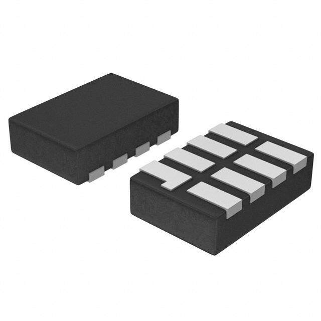
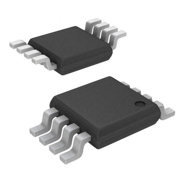
| 供应商器件封装 | TSOT-23-6 |
| 元件数 | 2 |
| 其它名称 | LT6700IS6-1#TRMPBFCT |
| 包装 | 剪切带 (CT) |
| 安装类型 | 表面贴装 |
| 封装/外壳 | SOT-23-6 细型,TSOT-23-6 |
| 工作温度 | -40°C ~ 85°C |
| 标准包装 | 1 |
| 滞后 | 11.5mV |
| 电压-电源,单/双 (±) | 1.4 V ~ 18 V |
| 电压-输入失调(最大值) | - |
| 电流-输入偏置(最大值) | 0.01µA @ 18V |
| 电流-输出(典型值) | - |
| 电流-静态(最大值) | 17µA |
| 类型 | 通用 |
| 输出类型 | 开路集电极 |


- 商务部:美国ITC正式对集成电路等产品启动337调查
- 曝三星4nm工艺存在良率问题 高通将骁龙8 Gen1或转产台积电
- 太阳诱电将投资9.5亿元在常州建新厂生产MLCC 预计2023年完工
- 英特尔发布欧洲新工厂建设计划 深化IDM 2.0 战略
- 台积电先进制程称霸业界 有大客户加持明年业绩稳了
- 达到5530亿美元!SIA预计今年全球半导体销售额将创下新高
- 英特尔拟将自动驾驶子公司Mobileye上市 估值或超500亿美元
- 三星加码芯片和SET,合并消费电子和移动部门,撤换高东真等 CEO
- 三星电子宣布重大人事变动 还合并消费电子和移动部门
- 海关总署:前11个月进口集成电路产品价值2.52万亿元 增长14.8%


PDF Datasheet 数据手册内容提取
LT6700/LT6700HV Micropower, Low Voltage, Dual Comparator with 400mV Reference FEATURES DESCRIPTION n Internal 400mV Reference The LT®6700/LT6700HV combine two micropower, low n Total Threshold Error: ±1.25% Max at 25°C voltage comparators with a 400mV reference in a 6-lead n Inputs and Outputs Operate to 36V SOT-23 or tiny DFN package. Operating with supplies from n Wide Supply Range: 1.4V to 18V 1.4V up to 18V, these devices draw only 6.5µA, making n Specified for –55°C to 125°C Temperature Range them ideal for low voltage system monitoring. Hysteresis n Low Quiescent Current: 6.5µA Typ at 5V is included in the comparators, easing design requirements n Internal Hysteresis: 6.5mV Typ to insure stable output operation. n Low Input Bias Current: ±10nA Max The comparators each have one input available externally; n Over-The-Top® Input also Includes Ground the other inputs are connected internally to the reference. n Open-Collector Outputs Allow Level Translation The comparator outputs are open collector and the output n Choice of Input Polarities: LT6700-1/LT6700-2/ load can be referred to any voltage up to 18V (36V for LT6700-3/LT6700HV-1/LT6700HV-2/LT6700HV-3 LT6700HV), independent of supply voltage. The output n Available in Low Profile (1mm) SOT-23 (ThinSOT™) stage sinking capability is guaranteed to be greater than and 2mm × 3mm DFN Packages 5mA over temperature. APPLICATIONS The three versions of this part differ by the polar- ity of the available comparator inputs. The LT6700-1/ n Battery-Powered System Monitoring LT6700HV-1 has one inverting input and one noninvert- n Threshold Detectors ing input, making it suitable for use as a window com- n Window Comparators parator. The LT6700-2/LT6700HV-2 has two inverting n Relay Driving inputs and the LT6700-3/LT6700HV-3 has two nonin- n Industrial Control Systems verting inputs. All versions are offered in commercial, n Handheld Instruments industrial and automotive temperature ranges. n Automotive Monitor and Controls L, LT, LTC, LTM, Linear Technology, the Linear logo and Over-The-Top are registered trademarks and ThinSOT and PowerPath are trademarks of Linear Technology Corporation. All other trademarks are the property of their respective owners. TYPICAL APPLICATION Micropower Battery Monitor Comparator Thresholds VBATT vs Temperature 1.4V (MIN) 3V (NOM) 1M LT6700-3 1M 1M 406 #1A #2A + COMP B 404 #1B #2B RISING INPUT + 0.1µF 63.4k – VBATT > 1.6V OLTAGE (mV)440002 AALAK CAELLINLSE + VR = 400mV VS OLD V398 REFERENCE SH396 FALLING INPUT RE H394 – COMP A T TWO TYPICAL PARTS 392 COMP A AND B VBATT > 2V VS = 5V + MONITOR CONSUMES ~10µA 390–60–40–20 0 20 40 60 80 100120 261k HYSTERESIS IS APPROXIMATELY TEMPERATURE (°C) 2% OF TRIP VOLTAGE 6700123 TA02 6700123 TA01 6700123fh 1 For more information www.linear.com/LT6700
LT6700/LT6700HV ABSOLUTE MAXIMUM RATINGS (Note 1) Total Supply Voltage (V to GND) ..........................18.5V Specified Temperature Range (Note 5) S Input Voltage (+IN, –IN) LT6700CS6/LT6700HVCS6/ LT6700 (Note 3) ..........................18.5V to (GND – 0.3V) LT6700CDCB-1/-2/-3 ..............................0°C to 70°C LT6700HV (Note 3) ........................40V to (GND – 0.3V) LT6700IS6/LT6700HVIS6/ LT6700 Output Voltage (OUT) .....18.5V to (GND – 0.3V) LT6700IDCB-1/-2/-3 ............................–40°C to 85°C LT6700HV Output Voltage (OUT) ...40V to (GND – 0.3V) LT6700HS6/LT6700HVHS6/ Output Short-Circuit Duration (Note 2) ............Indefinite LT6700HDCB-1/-2/-3 .......................–40°C to 125°C Input Current (Note 3) ..........................................–10mA LT6700MPDCB/ Operating Temperature Range (Note 4) LT6700PMS6-1/-2/-3 .........................–55°C to 125°C LT6700CS6/LT6700HVCS6/ Maximum Junction Temperature LT6700CDCB-1/-2/-3 ...........................–40°C to 85°C S6 Package .......................................................150°C LT6700IS6/LT6700HVIS6/ DCB6 Package ..................................................150°C LT6700IDCB-1/-2/-3 ............................–40°C to 85°C Storage Temperature Range LT6700HS6/LT6700HVHS6/ S6 Package ........................................–65°C to 150°C LT6700HDCB-1/-2/-3 ........................–40°C to 125°C DCB6 Package ...................................–65°C to 150°C LT6700MPDCB/ Lead Temperature, TSOT-23 (Soldering, 10 sec) ...300°C LT6700MPS6-1/-2/-3 .........................–55°C to 125°C PIN CONFIGURATION LT6700-1 LT6700-2 LT6700-3 LT6700HV-1 LT6700HV-2 LT6700HV-3 TOP VIEW TOP VIEW TOP VIEW OUTA 1 6 OUTB OUTA 1 6 OUTB OUTA 1 6 OUTB GND 2 5 VS GND 2 5 VS GND 2 5 VS +INA 3 4 –INB –INA 3 4 –INB +INA 3 4 +INB S6 PACKAGE S6 PACKAGE S6 PACKAGE 6-LEAD PLASTIC TSOT-23 6-LEAD PLASTIC TSOT-23 6-LEAD PLASTIC TSOT-23 TJMAX = 150°C, θJA = 230°C/W TJMAX = 150°C, θJA = 230°C/W TJMAX = 150°C, θJA = 230°C/W LT6700-1 LT6700-2 LT6700-3 TOP VIEW TOP VIEW TOP VIEW OUTA 1 6 + INA OUTA 1 6 – INA OUTA 1 6 + INA OUTB 2 7 5 GND OUTB 2 7 5 GND OUTB 2 7 5 GND VS 3 4 –INB VS 3 4 –INB VS 3 4 +INB DCB6 PACKAGE DCB6 PACKAGE DCB6 PACKAGE 6-LEAD (2mm × 3mm) PLASTIC DFN 6-LEAD (2mm × 3mm) PLASTIC DFN 6-LEAD (2mm × 3mm) PLASTIC DFN TJMAX = 125°C, θJA = 64°C/W TJMAX = 125°C, θJA = 64°C/W TJMAX = 125°C, θJA = 64°C/W SOLDERED EXPOSED PAD (PIN 7) SOLDERED EXPOSED PAD (PIN 7) SOLDERED EXPOSED PAD (PIN 7) INTERNALLY CONNECTED TO GND INTERNALLY CONNECTED TO GND INTERNALLY CONNECTED TO GND (PCB CONNECTION OPTIONAL) (PCB CONNECTION OPTIONAL) (PCB CONNECTION OPTIONAL) 6700123fh 2 For more information www.linear.com/LT6700
LT6700/LT6700HV ORDER INFORMATION Lead Free Finish TAPE AND REEL (MINI) TAPE AND REEL PART MARKING* PACKAGE DESCRIPTION SPECIFIED TEMPERATURE RANGE LT6700CS6-1#TRMPBF LT6700CS6-1#TRPBF LTK7 6-Lead Plastic TSOT-23 0°C to 70°C LT6700HVCS6-1#TRMPBF LT6700HVCS6-1#TRPBF LTK7 6-Lead Plastic TSOT-23 0°C to 70°C LT6700IS6-1#TRMPBF LT6700IS6-1#TRPBF LTK7 6-Lead Plastic TSOT-23 –40°C to 85°C LT6700HVIS6-1#TRMPBF LT6700HVIS6-1#TRPBF LTK7 6-Lead Plastic TSOT-23 –40°C to 85°C LT6700HS6-1#TRMPBF LT6700HS6-1#TRPBF LTK7 6-Lead Plastic TSOT-23 –40°C to 125°C LT6700HVHS6-1#TRMPBF LT6700HVHS6-1#TRPBF LTK7 6-Lead Plastic TSOT-23 –40°C to 125°C LT6700MPS6-1#TRMPBF LT6700MPS6-1#TRPBF LTK7 6-Lead Plastic TSOT-23 –55°C to 125°C LT6700CS6-2#TRMPBF LT6700CS6-2#TRPBF LTADL 6-Lead Plastic TSOT-23 0°C to 70°C LT6700HVCS6-2#TRMPBF LT6700HVCS6-2#TRPBF LTADL 6-Lead Plastic TSOT-23 0°C to 70°C LT6700IS6-2#TRMPBF LT6700IS6-2#TRPBF LTADL 6-Lead Plastic TSOT-23 –40°C to 85°C LT6700HVIS6-2#TRMPBF LT6700HVIS6-2#TRPBF LTADL 6-Lead Plastic TSOT-23 –40°C to 85°C LT6700HS6-2#TRMPBF LT6700HS6-2#TRPBF LTADL 6-Lead Plastic TSOT-23 –40°C to 125°C LT6700HVHS6-2#TRMPBF LT6700HVHS6-2#TRPBF LTADL 6-Lead Plastic TSOT-23 –40°C to 125°C LT6700MPS6-2#TRMPBF LT6700MPS6-2#TRPBF LTADL 6-Lead Plastic TSOT-23 –55°C to 125°C LT6700CS6-3#TRMPBF LT6700CS6-3#TRPBF LTADM 6-Lead Plastic TSOT-23 0°C to 70°C LT6700HVCS6-3#TRMPBF LT6700HVCS6-3#TRPBF LTADM 6-Lead Plastic TSOT-23 0°C to 70°C LT6700IS6-3#TRMPBF LT6700IS6-3#TRPBF LTADM 6-Lead Plastic TSOT-23 –40°C to 85°C LT6700HVIS6-3#TRMPBF LT6700HVIS6-3#TRPBF LTADM 6-Lead Plastic TSOT-23 –40°C to 85°C LT6700HS6-3#TRMPBF LT6700HS6-3#TRPBF LTADM 6-Lead Plastic TSOT-23 –40°C to 125°C LT6700HVHS6-3#TRMPBF LT6700HVHS6-3#TRPBF LTADM 6-Lead Plastic TSOT-23 –40°C to 125°C LT6700MPS6-3#TRMPBF LT6700MPS6-2 #TRPBF LTADM 6-Lead Plastic TSOT-23 –55°C to 125°C LT6700CDCB-1#TRMPBF LT6700CDCB-1#TRPBF LBXW 6-Lead (2mm × 3mm) Plastic DFN 0°C to 70°C LT6700IDCB-1#TRMPBF LT6700IDCB-1#TRPBF LBXW 6-Lead (2mm × 3mm) Plastic DFN –40°C to 85°C LT6700HDCB-1#TRMPBF LT6700HDCB-1#TRPBF LBXW 6-Lead (2mm × 3mm) Plastic DFN –40°C to 125°C LT6700MPDCB-1#TRMPBF LT6700MPDCB-1#TR LDVS 6-Lead (2mm × 3mm) Plastic DFN –55°C to 125°C LT6700CDCB-2#TRMPBF LT6700CDCB-2#TRPBF LBXX 6-Lead (2mm × 3mm) Plastic DFN 0°C to 70°C LT6700IDCB-2#TRMPBF LT6700IDCB-2#TRPBF LBXX 6-Lead (2mm × 3mm) Plastic DFN –40°C to 85°C LT6700HDCB-2#TRMPBF LT6700HDCB-2#TRPBF LBXX 6-Lead (2mm × 3mm) Plastic DFN –40°C to 125°C LT6700MPDCB-2#TRMPBF LT6700MPDCB-2#TR LDVT 6-Lead (2mm × 3mm) Plastic DFN –55°C to 125°C LT6700CDCB-3#TRMPBF LT6700CDCB-3#TRPBF LBXY 6-Lead (2mm × 3mm) Plastic DFN 0°C to 70°C LT6700IDCB-3#TRMPBF LT6700IDCB-3#TRPBF LBXY 6-Lead (2mm × 3mm) Plastic DFN –40°C to 85°C LT6700HDCB-3#TRMPBF LT6700HDCB-3#TRPBF LBXY 6-Lead (2mm × 3mm) Plastic DFN –40°C to 125°C LT6700MPDCB-3#TRMPBF LT6700MPDCB-3#TR LDVV 6-Lead (2mm × 3mm) Plastic DFN –55°C to 125°C TRM = 500 pieces. *Temperature grades are identified by a label on the shipping container. Consult LTC Marketing for parts specified with wider operating temperature ranges. Consult LTC Marketing for information on lead based finish parts. For more information on lead free part marking, go to: http://www.linear.com/leadfree/ For more information on tape and reel specifications, go to: http://www.linear.com/tapeandreel/ 6700123fh 3 For more information www.linear.com/LT6700
LT6700/LT6700HV ELECTRICAL CHARACTERISTICS T = 25°C, (LT6700-1/LT6700-2/LT6700-3) unless otherwise specified. A SYMBOL PARAMETER CONDITIONS MIN TYP MAX UNITS V Rising Input Threshold Voltage (Note 6) R = 100k, V = 2V Swing TH(R) L O V = 1.4V 394 400 406 mV S V = 5V 395 400 405 mV S V = 12V 393 400 407 mV S V = 18V 392 400 408 mV S V Falling Input Threshold Voltage (Note 6) R = 100k, V = 2V Swing TH(F) L O V = 1.4V 386 393.5 401 mV S V = 5V 387 393.5 400 mV S V = 12V 385 393.5 402 mV S V = 18V 384 393.5 403 mV S HYS HYS = V – V V = 1.4V, 5V, 12V, 18V, R = 100k, V = 2V Swing 3.5 6.5 9.5 mV TH(R) TH(F) S L O I Input Bias Current V = 1.4V, 18V, V = V ±0.01 ±10 nA B S IN S V = 1.4V, V = 18V ±0.01 ±10 nA S IN V = 1.4V, 18V, V = 0.1V ±4 ±10 nA S IN V Output Low Voltage 10mV Input Overdrive OL V = 1.4V, I = 0.5mA 55 200 mV S OUT V = 1.6V, I = 3mA 60 200 mV S OUT V = 5V, I = 5mA 70 200 mV S OUT I Output Leakage Current V = 1.4V, 18V, V = V , V = 40mV Overdrive 0.01 0.8 µA OFF S OUT S IN V = 1.4V, V = 18V, V = 40mV Overdrive 0.01 0.8 µA S OUT IN t High-to-Low Propagation Delay V = 5V, 10mV Input Overdrive, R = 10k, 18 µs PD(HL) S L V = 400mV OL t Low-to-High Propagation Delay V = 5V, 10mV Input Overdrive, R = 10k, 29 µs PD(LH) S L V = 0.9 • V OH S t Output Rise Time V = 5V, 10mV Input Overdrive, R = 10k 2.2 µs r S L V = (0.1 to 0.9) • V O S t Output Fall Time V = 5V, 10mV Input Overdrive, R = 10k 0.22 µs f S L V = (0.1 to 0.9) • V O S I Supply Current No Load Current S V = 1.4V 5.7 10.0 µA S V = 5V 6.5 11.0 µA S V = 12V 6.9 12.5 µA S V = 18V 7.1 13.0 µA S The l denotes the specifications which apply over the temperature range of 0°C ≤ T ≤ 70°C, (LT6700C-1/LT6700C-2/LT6700C-3) unless A otherwise specified (Notes 4, 5). SYMBOL PARAMETER CONDITIONS MIN TYP MAX UNITS V Rising Input Threshold Voltage (Note 6) R = 100k, V = 2V Swing TH(R) L O V = 1.4V l 391.0 409.0 mV S V = 5V l 392.5 407.5 mV S V = 12V l 390.0 410.0 mV S V = 18V l 389.0 411.0 mV S V Falling Input Threshold Voltage (Note 6) R = 100k, V = 2V Swing TH(F) L O V = 1.4V l 383.5 403.5 mV S V = 5V l 384.5 402.5 mV S V = 12V l 382.5 404.5 mV S V = 18V l 381.5 405.5 mV S 6700123fh 4 For more information www.linear.com/LT6700
LT6700/LT6700HV ELECTRICAL CHARACTERISTICS The l denotes the specifications which apply over the temperature range of 0°C ≤ T ≤ 70°C, (LT6700C-1/LT6700C-2/LT6700C-3) unless A otherwise specified (Notes 4, 5). SYMBOL PARAMETER CONDITIONS MIN TYP MAX UNITS HYS HYS = V – V V = 1.4V, 5V, 12V, 18V, R = 100k, V = 2V Swing l 3 11 mV TH(R) TH(F) S L O I Input Bias Current V = 1.4V, 18V, V = V l ±15 nA B S IN S V = 1.4V, V = 18V l ±15 nA S IN V = 1.4V, 18V, V = 0.1V l ±15 nA S IN V Output Low Voltage 10mV Input Overdrive OL V = 1.4V, I = 0.5mA l 250 mV S OUT V = 1.6V, I = 3mA l 250 mV S OUT V = 5V, I = 5mA l 250 mV S OUT I Output Leakage Current V = 1.4V, 18V, V = V , V = 40mV Overdrive l 1 µA OFF S OUT S IN V = 1.4V, V = 18V, V = 40mV Overdrive l 1 µA S OUT IN I Supply Current No Load Current S V = 1.4V l 13.0 µA S V = 5V l 14.0 µA S V = 12V l 15.5 µA S VS = 18V l 16.0 µA The l denotes the specifications which apply over the temperature range of –40°C ≤ T ≤ 85°C, (LT6700I-1/LT6700I-2/LT6700I-3) A unless otherwise specified (Notes 4, 5). SYMBOL PARAMETER CONDITIONS MIN TYP MAX UNITS V Rising Input Threshold Voltage (Note 6) R = 100k, V = 2V Swing TH(R) L O V = 1.4V l 390 410 mV S V = 5V l 392 408 mV S V = 12V l 389 411 mV S V = 18V l 388 412 mV S V Falling Input Threshold Voltage (Note 6) R = 100k, V = 2V Swing TH(F) L O V = 1.4V l 382.5 404.5 mV S V = 5V l 383.5 403.5 mV S V = 12V l 381.5 405.5 mV S V = 18V l 380.5 406.5 mV S HYS HYS = V – V V = 1.4V, 5V, 12V, 18V, R = 100k, V = 2V Swing l 2 11.5 mV TH(R) TH(F) S L O I Input Bias Current V = 1.4V, 18V, V = V l ±15 nA B S IN S V = 1.4V, V = 18V l ±15 nA S IN V = 1.4V, 18V, V = 0.1V l ±15 nA S IN V Output Low Voltage 10mV Input Overdrive OL V = 1.4V, I = 0.1mA l 250 mV S OUT V = 1.6V, I = 3mA l 250 mV S OUT V = 5V, I = 5mA l 250 mV S OUT I Output Leakage Current V = 1.4V, 18V, V = V , V = 40mV Overdrive l 1 µA OFF S OUT S IN V = 1.4V, V = 18V, V = 40mV Overdrive l 1 µA S OUT IN I Supply Current No Load Current S V = 1.4V l 14.0 µA S V = 5V l 15.0 µA S V = 12V l 16.5 µA S V = 18V l 17.0 µA S 6700123fh 5 For more information www.linear.com/LT6700
LT6700/LT6700HV ELECTRICAL CHARACTERISTICS The l denotes the specifications which apply over the temperature range of –40°C ≤ T ≤ 125°C, (LT6700H-1/LT6700H-2/LT6700H-3) A unless otherwise specified (Notes 4, 5). LT6700H SYMBOL PARAMETER CONDITIONS MIN TYP MAX UNITS V Rising Input Threshold Voltage (Note 6) R = 100k, V = 2V Swing TH(R) L O V = 1.4V l 390 411 mV S V = 5V l 392 410 mV S V = 12V l 389 412 mV S V = 18V l 388 413 mV S V Falling Input Threshold Voltage (Note 6) R = 100k, V = 2V Swing TH(F) L O V = 1.4V l 381.5 405.5 mV S V = 5V l 382.5 404.5 mV S V = 12V l 380.5 406.5 mV S V = 18V l 379.5 407.5 mV S HYS HYS = V – V V = 1.4V, 5V, 12V, 18V, R = 100k, V = 2V Swing l 2 13.5 mV TH(R) TH(F) S L O I Input Bias Current V = 1.4V, 18V, V = V l ±45 nA B S IN S V = 1.4V, V = 18V l ±45 nA S IN V = 1.4V, 18V, V = 100mV l ±50 nA S IN V Output Low Voltage 10mV Input Overdrive OL V = 1.4V, I = 0.1mA l 250 mV S OUT V = 1.6V, I = 3mA l 250 mV S OUT V = 5V, I = 5mA l 250 mV S OUT I Output Leakage Current V = 1.4V, 18V, V = V , V = 40mV Overdrive l 1 µA OFF S OUT S IN V = 1.4V, V = 18V, V = 40mV Overdrive l 1 µA S OUT IN I Supply Current No Load Current S V = 1.4V l 16.0 µA S V = 5V l 17.0 µA S V = 12V l 18.5 µA S VS = 18V l 19.0 µA The l denotes the specifications which apply over the temperature range of –55°C ≤ T ≤ 125°C, (LT6700MP-1/LT6700MP-2/LT6700MP-3) A unless otherwise specified (Notes 4, 5). LT6700H SYMBOL PARAMETER CONDITIONS MIN TYP MAX UNITS V Rising Input Threshold Voltage (Note 6) R = 100k, V = 2V Swing TH(R) L O V = 1.4V l 390 411 mV S V = 5V l 392 410 mV S V = 12V l 389 412 mV S V = 18V l 388 413 mV S V Falling Input Threshold Voltage (Note 6) R = 100k, V = 2V Swing TH(F) L O V = 1.4V l 381.5 405.5 mV S V = 5V l 382.5 404.5 mV S V = 12V l 380.5 406.5 mV S V = 18V l 379.5 407.5 mV S HYS HYS = V – V V = 1.4V, 5V, 12V, 18V, R = 100k, V = 2V Swing l 2 13.5 mV TH(R) TH(F) S L O I Input Bias Current V = 1.4V, 18V, V = V l ±45 nA B S IN S V = 1.4V, V = 18V l ±45 nA S IN V = 1.4V, 18V, V = 100mV l ±50 nA S IN V Output Low Voltage 10mV Input Overdrive OL V = 1.4V, I = 0.1mA l 250 mV S OUT V = 1.6V, I = 3mA l 250 mV S OUT V = 5V, I = 5mA l 250 mV S OUT 6700123fh 6 For more information www.linear.com/LT6700
LT6700/LT6700HV ELECTRICAL CHARACTERISTICS The l denotes the specifications which apply over the temperature range of –55°C ≤ T ≤ 125°C, (LT6700MP-1/LT6700MP-2/LT6700MP-3) A unless otherwise specified (Notes 4, 5). LT6700H SYMBOL PARAMETER CONDITIONS MIN TYP MAX UNITS I Output Leakage Current V = 1.4V, 18V, V = V , V = 40mV Overdrive l 1 µA OFF S OUT S IN V = 18V, V = 18V, V = 40mV Overdrive l 1 µA S OUT IN I Supply Current No Load Current S V = 1.4V l 16.0 µA S V = 5V l 17.0 µA S V = 12V l 18.5 µA S VS = 18V l 19.0 µA T = 25°C, (LT6700HV-1/LT6700HV-2/LT6700HV-3) unless otherwise specified. A SYMBOL PARAMETER CONDITIONS MIN TYP MAX UNITS V Rising Input Threshold Voltage (Note 6) R = 100k, V = 2V Swing TH(R) L O V = 1.4V 394 400 406 mV S V = 5V 395 400 405 mV S V = 12V 393 400 407 mV S V = 18V 392 400 408 mV S V Falling Input Threshold Voltage (Note 6) R = 100k, V = 2V Swing TH(F) L O V = 1.4V 386 393.5 401 mV S V = 5V 387 393.5 400 mV S V = 12V 385 393.5 402 mV S V = 18V 384 393.5 403 mV S HYS HYS = V – V V = 1.4V, 5V, 12V, 18V, R = 100k, V = 2V Swing 3.5 6.5 9.5 mV TH(R) TH(F) S L O I Input Bias Current V = 1.4V, 18V, V = V ±0.01 ±10 nA B S IN S V = 1.4V, V = 18V, 36V ±0.01 ±10 nA S IN V = 1.4V, 18V, V = 0.1V ±4 ±10 nA S IN V Output Low Voltage 10mV Input Overdrive OL V = 1.4V, I = 0.5mA 55 200 mV S OUT V = 1.6V, I = 3mA 60 200 mV S OUT V = 5V, I = 5mA 70 200 mV S OUT I Output Leakage Current V = 1.4V, 18V, V = V , V = 40mV Overdrive 0.01 0.8 µA OFF S OUT S IN V = 18V, V = 18V, (36V, R = 100k), V = 40mV Overdrive 0.01 0.8 µA S OUT L IN t High-to-Low Propagation Delay V = 5V, 10mV Input Overdrive, R = 10k, 18 µs PD(HL) S L V = 400mV OL t Low-to-High Propagation Delay V = 5V, 10mV Input Overdrive, R = 10k, 29 µs PD(LH) S L V = 0.9 • V OH S t Output Rise Time V = 5V, 10mV Input Overdrive, R = 10k 2.2 µs r S L V = (0.1 to 0.9) • V O S t Output Fall Time V = 5V, 10mV Input Overdrive, R = 10k 0.22 µs f S L V = (0.1 to 0.9) • V O S I Supply Current No Load Current S V = 1.4V 5.7 10.0 µA S V = 5V 6.5 11.0 µA S V = 12V 6.9 12.5 µA S V = 18V 7.1 13.0 µA S 6700123fh 7 For more information www.linear.com/LT6700
LT6700/LT6700HV ELECTRICAL CHARACTERISTICS The l denotes the specifications which apply over the temperature range of 0°C ≤ T ≤ 70°C, (LT6700HVC-1/LT6700HVC-2/LT6700HVC-3) A unless otherwise specified (Notes 4, 5). SYMBOL PARAMETER CONDITIONS MIN TYP MAX UNITS V Rising Input Threshold Voltage R = 100k, V = 2V Swing TH(R) L O (Note 6) V = 1.4V l 391.0 409.0 mV S V = 5V l 392.5 407.5 mV S V = 12V l 390.0 410.0 mV S V = 18V l 389.0 411.0 mV S V Falling Input Threshold Voltage R = 100k, V = 2V Swing TH(F) L O (Note 6) V = 1.4V l 383.5 403.5 mV S V = 5V l 384.5 402.5 mV S V = 12V l 382.5 404.5 mV S V = 18V l 381.5 405.5 mV S HYS HYS = V – V V = 1.4V, 5V, 12V, 18V, R = 100k, V = 2V Swing l 3 11 mV TH(R) TH(F) S L O I Input Bias Current V = 1.4V, 18V, V = V l ±15 nA B S IN S V = 1.4V, V = 18V, 36V l ±15 nA S IN V = 1.4V, 18V, V = 0.1V l ±15 nA S IN V Output Low Voltage 10mV Input Overdrive OL V = 1.4V, I = 0.5mA l 250 mV S OUT V = 1.6V, I = 3mA l 250 mV S OUT V = 5V, I = 5mA l 250 mV S OUT I Output Leakage Current V = 1.4V, 18V, V = V , V = 40mV Overdrive l 1 µA OFF S OUT S IN V = 18V, V = 18V, (36V, R = 100k), V = 40mV Overdrive l 1 µA S OUT L IN I Supply Current No Load Current S V = 1.4V l 13.0 µA S V = 5V l 14.0 µA S V = 12V l 15.5 µA S VS = 18V l 16.0 µA The l denotes the specifications which apply over the temperature range of –40°C ≤ T ≤ 85°C, (LT6700HVI-1/LT6700HVI-2/LT6700HVI-3) A unless otherwise specified (Notes 4, 5). SYMBOL PARAMETER CONDITIONS MIN TYP MAX UNITS V Rising Input Threshold Voltage (Note 6) R = 100k, V = 2V Swing TH(R) L O V = 1.4V l 390 410 mV S V = 5V l 392 408 mV S V = 12V l 389 411 mV S V = 18V l 388 412 mV S V Falling Input Threshold Voltage (Note 6) R = 100k, V = 2V Swing TH(F) L O V = 1.4V l 382.5 404.5 mV S V = 5V l 383.5 403.5 mV S V = 12V l 381.5 405.5 mV S V = 18V l 380.5 406.5 mV S HYS HYS = V – V V = 1.4V, 5V, 12V, 18V, R = 100k, V = 2V Swing l 2 11.5 mV TH(R) TH(F) S L O I Input Bias Current V = 1.4V, 18V, V = V l ±15 nA B S IN S V = 1.4V, V = 18V, 36V l ±15 nA S IN V = 1.4V, 18V, V = 0.1V l ±15 nA S IN V Output Low Voltage 10mV Input Overdrive OL V = 1.4V, I = 0.1mA l 250 mV S OUT V = 1.6V, I = 3mA l 250 mV S OUT V = 5V, I = 5mA l 250 mV S OUT I Output Leakage Current V = 1.4V, 18V, V = V , V = 40mV Overdrive l 1 µA OFF S OUT S IN V = 18V, V = 18V, (36V, R = 100k), V = 40mV Overdrive l 1 µA S OUT L IN 6700123fh 8 For more information www.linear.com/LT6700
LT6700/LT6700HV ELECTRICAL CHARACTERISTICS The l denotes the specifications which apply over the temperature range of –40°C ≤ T ≤ 85°C, (LT6700HVI-1/LT6700HVI-2/LT6700HVI-3) A unless otherwise specified (Notes 4, 5). SYMBOL PARAMETER CONDITIONS MIN TYP MAX UNITS I Supply Current No Load Current S V = 1.4V l 14.0 µA S V = 5V l 15.0 µA S V = 12V l 16.5 µA S V = 18V l 17.0 µA S The l denotes the specifications which apply over the temperature range of –40°C ≤ T ≤ 125°C, (LT6700HVH-1/LT6700HVH-2/ A LT6700HVH-3) unless otherwise specified (Notes 4, 5). LT6700H SYMBOL PARAMETER CONDITIONS MIN TYP MAX UNITS V Rising Input Threshold Voltage R = 100k, V = 2V Swing TH(R) L O (Note 6) V = 1.4V l 390 411 mV S V = 5V l 392 410 mV S V = 12V l 389 412 mV S V = 18V l 388 413 mV S V Falling Input Threshold Voltage R = 100k, V = 2V Swing TH(F) L O (Note 6) V = 1.4V l 381.5 405.5 mV S V = 5V l 382.5 404.5 mV S V = 12V l 380.5 406.5 mV S V = 18V l 379.5 407.5 mV S HYS HYS = V – V V = 1.4V, 5V, 12V, 18V, R = 100k, V = 2V Swing l 2 13.5 mV TH(R) TH(F) S L O I Input Bias Current V = 1.4V, 18V, V = V l ±45 nA B S IN S V = 1.4V, V = 18V, 36V l ±45 nA S IN V = 1.4V, 18V, V = 100mV l ±50 nA S IN V Output Low Voltage 10mV Input Overdrive OL V = 1.4V, I = 0.1mA l 250 mV S OUT V = 1.6V, I = 3mA l 250 mV S OUT V = 5V, I = 5mA l 250 mV S OUT I Output Leakage Current V = 1.4V, 18V, V = V , V = 40mV Overdrive l 1 µA OFF S OUT S IN V = 18V, V = 18V, (36V, R = 100k), V = 40mV Overdrive l 1 µA S OUT L IN I Supply Current No Load Current S V = 1.4V l 16.0 µA S V = 5V l 17.0 µA S V = 12V l 18.5 µA S VS = 18V l 19.0 µA Note 1: Stresses beyond those listed under Absolute Maximum Ratings temperature range of –40°C to 125°C. The LT6700MP-1/-2/-3 is may cause permanent damage to the device. Exposure to any Absolute guaranteed functional over the operating temperature range of –55°C to Maximum Rating condition for extended periods may affect device 125°C. reliability and lifetime. Note 5: The LT6700C-1/-2/-3/LT6700HVC-1/-2/-3 is guaranteed to meet the specified performance from 0°C to 70°C. The LT6700C-1/-2/- Note 2: A heat sink may be required to keep the junction temperature 3/LT6700HVC-1/-2/-3 are designed, characterized and expected to meet below the absolute maximum rating when the output is shorted specified performance from –40°C to 85°C but are not tested or QA indefinitely. sampled at these temperatures. The LT6700I-1/-2/-3/LT6700HVI-1/-2/-3 Note 3: The inputs are protected by ESD diodes to the ground. If the input is guaranteed to meet specified performance from –40°C to 85°C. The voltage exceeds –0.3V below ground, the input current should be limited LT6700H-1/-2/-3/LT6700HVH-1/-2/-3 is guaranteed to meet specified to less than 10mA. performance from –40°C to 125°C.The LT6700MP-1/-2/-3 is guaranteed to Note 4: The LT6700C-1/-2/-3/LT6700HVC-1/-2/-3, and meet specified performance from –55°C to 125°C. LT6700I-1/-2/-3/LT6700HVI-1/-2/-3 are guaranteed functional over the Note 6: V defines the threshold voltage of the comparators and operating temperature range of –40°C to 85°C. The LT6700H-1/-2/-3/ TH combines the effect of offset and reference accuracy. LT6700HVH-1/-2/-3 is guaranteed functional over the operating 6700123fh 9 For more information www.linear.com/LT6700
LT6700/LT6700HV PIN FUNCTIONS VS VS VS LT6700-1 LT6700-2 LT6700-3 LT6700HV-1 LT6700HV-2 LT6700HV-3 –INB – COMP B –INB – COMP B +INB + COMP B OUTB OUTB OUTB + + – 400mV VS 400mV VS 400mV VS REFERENCE REFERENCE REFERENCE – COMP A + COMP A – COMP A OUTA OUTA OUTA +INA + –INA – +INA + 6700123 PF01 6700123 PF02 6700123 PF03 GND GND GND OUTA: Open-Collector Output of Comparator Section A. INB: External Input for Comparator Section B. The volt- This pin provides drive for up to 40mA of load current. Off- age on this pin can range from –0.3V to 18V (36V for state voltage may be as high as 18V (36V for LT6700HV) LT6700HV) with respect to GND regardless of V used. S above GND, regardless of V used. The input is noninverting for the LT6700-3/LT6700HV-3, S and inverting for the LT6700-1/LT6700HV-1 and LT6700-2/ GND: Ground. This pin is also the low side return of the LT6700HV-2. The other section B comparator input is internal 400mV reference. internally connected to the 400mV reference. INA: External Input for Comparator Section A. The volt- V : Comparator Core Supply Voltage. The parts are char- age on this pin can range from –0.3V to 18V (36V for S acterized for operation with 1.4V ≤ V ≤ 18V with respect LT6700HV) with respect to GND regardless of V used. S S to GND. The input is noninverting for the LT6700-1/LT6700HV-1 and LT6700-3/LT6700HV-3, and inverting for the LT6700-2/ OUTB: Open-Collector Output of Comparator Section B. LT6700HV-2. The other section A comparator input is This pin provides drive for up to 40mA of load current. Off- internally connected to the 400mV reference. state voltage may be as high as 18V (36V for LT6700HV) above GND, regardless of V used. S 6700123fh 10 For more information www.linear.com/LT6700
LT6700/LT6700HV TYPICAL PERFORMANCE CHARACTERISTICS Distribution of Rising Input Distribution of Falling Input Threshold Voltage Threshold Voltage Distribution of Hysteresis 18 18 20 VS = 5V VS = 5V VS = 5V 16 TA = 25°C 16 TA = 25°C 18 TA = 25°C 16 14 14 %) %) %) 14 S ( 12 S ( 12 S ( UNIT 10 UNIT 10 UNIT 12 NT OF 8 NT OF 8 NT OF 180 RCE 6 RCE 6 RCE 6 PE PE PE 4 4 4 2 2 2 0 0 0 394 396 398 400 402 404 406 388 390 392 394 396 398 400 4 4.8 5.6 6.4 7.2 8 8.8 RISING INPUT THRESHOLD VOLTAGE (mV) FALLING INPUT THRESHOLD VOLTAGE (mV) HYSTERESIS (mV) 6700123 G01 6700123 G02 6700123 G03 Rising Input Threshold Voltage Rising Input Threshold Voltage Rising Input Threshold Voltage vs Temperature vs Temperature vs Supply Voltage 404 403.0 403.0 V) FOUR TYPICAL PARTS V) VS = 1.4V V) TA = 25°C GE (m 403 #1 VS = 5V GE (m402.5 VVSS == 51V2V GE (m402.5 TTAA == 8152°5C°C OLTA 402 OLTA402.0 VS = 18V OLTA402.0 TA = –55°C V #2 V V D 401 D 401.5 D 401.5 OL OL OL SH 400 SH401.0 SH401.0 RE #3 RE RE H H H UT T 399 UT T400.5 UT T400.5 NP 398 NP400.0 NP400.0 SING I 397 #4 SING I399.5 SING I399.5 RI RI RI 396 399.0 399.0 –60 –40 –20 0 20 40 60 80 100 120 –60 –40 –20 0 20 40 60 80 100 120 2 4 6 8 10 12 14 16 18 TEMPERATURE (°C) TEMPERATURE (°C) SUPPLY VOLTAGE (V) 6700123 G04 6700123 G05 6700123 G06 Hysteresis vs Temperature Hysteresis vs Temperature Hysteresis vs Supply Voltage 10 10 10 FOUR TYPICAL PARTS VS = 1.4V TA = 25°C TA = 125°C 9 VS = 5V 9 VS = 5V 9 TA = 85°C TA = –55°C #1 VS = 12V 8 #2 8 VS = 18V 8 V) #3 V) V) S (m 7 #4 S (m 7 S (m 7 RESI 6 RESI 6 RESI 6 YSTE 5 YSTE 5 YSTE 5 H H H 4 4 4 3 3 3 2 2 2 –60 –40 –20 0 20 40 60 80 100 120 –60 –40 –20 0 20 40 60 80 100 120 2 4 6 8 10 12 14 16 18 TEMPERATURE (°C) TEMPERATURE (°C) SUPPLY VOLTAGE (V) 6700123 G07 6700123 G08 6700123 G09 6700123fh 11 For more information www.linear.com/LT6700
LT6700/LT6700HV TYPICAL PERFORMANCE CHARACTERISTICS Quiescent Supply Current Minimum Supply Voltage vs Supply Voltage Start-Up Supply Current 1 10 50 TA = 25°C TA = 125°C TA = 25°C TA = 85°C TA = –55°C TA = 85°C 0 9 NO LOAD CURRENT 40 TA = 125°C V) A) A) TA = –55°C m µ µ D SHIFT ( ––12 URRENT ( 78 URRENT ( 30 L C C THRESHO –3 TA = 25°C SUPPLY 6 SUPPLY 2100 –4 TA = 85°C 5 TA = 125°C TA = –55°C –5 4 0 0.9 1.1 1.3 1.5 1.7 1.9 1.4 3.4 5.4 7.4 9.4 11.4 13.4 15.4 17.4 0 0.2 0.4 0.6 0.8 1.0 1.2 1.4 SUPPLY VOLTAGE (V) SUPPLY VOLTAGE (V) SUPPLY VOLTAGE (V) 6700123 G10 6700123 G11 6700123 G12 Supply Current Supply Current Supply Current vs Output Sink Current vs Output Sink Current vs Output Sink Current 1000 1000 1000 TA = –40°C TA = 25°C TA = 85°C VS = 1.4V VS = 1.4V VS = 1.4V VS = 5V VS = 5V VS = 5V NT (µA)100 VVSS == 1128VV NT (µA)100 VVSS == 1128VV NT (µA)100 VVSS == 1128VV RE RE RE R R R U U U UPPLY C 10 UPPLY C 10 UPPLY C 10 S S S 1 1 1 0.001 0.01 0.1 1 10 100 0.001 0.01 0.1 1 10 100 0.001 0.01 0.1 1 10 100 OUTPUT SINK CURRENT (mA) OUTPUT SINK CURRENT (mA) OUTPUT SINK CURRENT (mA) 6700123 G13 6700123 G14 6700123 G15 Below Ground Input Bias Current Low Level Input Bias Current High Level Input Bias Current 10000 3 10 VS = 18V CURRENT IS POSITIVE GOING CURRENT IS GOING INTO THE DEVICE –0.3V < VIB < 0V 2 INTO THE DEVICE TA = 25°C 1 A)1000 TA = 85°C A) A) 1 NT (n TTAA == 1–2555°°CC NT (n 0 NT (n RE RE –1 RE R R R CU 100 CU –2 CU 0.1 S S S INPUT BIA 10 INPUT BIA –––435 0VVS =< 1V8IBVTT AA< ==1 V2855°°CC INPUT BIA 0.01 VVSIB => 118VTVA = 25°C –6 TA = 125°C TA = 85°C CURRENT IS GOING OUT OF THE DEVICE TA = –55°C TA = 125°C 1 –7 0.001 –0.3 –0.2 –0.1 0 0 0.1 0.2 0.3 0.4 0.5 0.6 0.7 0.8 0.9 1 1 3 5 7 9 11 13 15 17 INPUT VOLTAGE (V) INPUT VOLTAGE (V) INPUT VOLTAGE (V) 6700123 G16 6700123 G17 6700123 G18 6700123fh 12 For more information www.linear.com/LT6700
LT6700/LT6700HV TYPICAL PERFORMANCE CHARACTERISTICS Output Saturation Voltage Output Saturation Voltage Output Saturation Voltage vs Output Sink Current vs Output Sink Current vs Output Sink Current 1000 1000 1000 TA = –40°C TA = 25°C TA = 85°C V) VS = 1.4V V) VS = 1.4V V) VS = 1.4V GE (m VVSS == 51V2V GE (m VVSS == 51V2V GE (m VVSS == 51V2V LTA100 VS = 18V LTA100 VS = 18V LTA100 VS = 18V O O O V V V N N N O O O TI TI TI A A A R R R U U U AT 10 AT 10 AT 10 S S S T T T U U U P P P T T T U U U O O O 1 1 1 0.001 0.01 0.1 1 10 100 0.001 0.01 0.1 1 10 100 0.001 0.01 0.1 1 10 100 OUTPUT SINK CURRENT (mA) OUTPUT SINK CURRENT (mA) OUTPUT SINK CURRENT (mA) 6700123 G19 6700123 G20 6700123 G21 Output Short-Circuit Current Output Short-Circuit Current Output Leakage Current 80 80 10 70 70 A) A) A) CIRCUIT CURRENT (m 45630000 CIRCUIT CURRENT (m 45630000 T A = 25°VVVVCSSSS ==== 1511.V284VVV LEAKAGE CURRENT (n 0.11 VS = 5VTTAA == 2855°°CC SHORT- 20 VS = 5VTTAA == 2855°°CC SHORT- 20 OUTPUT 0.01 TTAA == 1–2555°°CC 10 TA = 125°C 10 TA = –55°C 0 0 0.001 0 2 4 6 8 10 12 14 16 18 0 2 4 6 8 10 12 14 16 18 0 2 4 6 8 10 12 14 16 18 OUTPUT VOLTAGE (V) OUTPUT VOLTAGE (V) OUTPUT VOLTAGE (V) 6700123 G22 6700123 G23 6700123 G24 Propagation Delay Rise and Fall Times Noninverting and Inverting vs Input Overdrive vs Output Pull-Up Resistor Comparator Propagation Delay 60 100 TA = 25°C LHHL NNOONNIINNVV CVSL == 250VpF VO(NINV) 50 LH INV TA = 25°C 5V/DIV ON DELAY (µs) 4300 HL INV ALL TIME (µs) 110 RISE FALL V5OV(/IDNDDIVCVC) GATI ND F 10mV/DVIIVN PA 20 E A AC O S PR RI 0.1 10 VS = 15V 20µs/DIV 6700123 G27 TA = 25°C 0 0.01 RLOAD = 10k CONNNECTED TO VS 0 20 40 60 80 100 0.1 1 10 100 1000 VIN(OVERDRIVE) = 10mV OVER THE INPUT VOLTAGE THRESHOLDS INPUT OVERDRIVE (mV) OUTPUT PULL-UP RESISTOR (kΩ) 6700123 G25 6700123 G26 6700123fh 13 For more information www.linear.com/LT6700
LT6700/LT6700HV APPLICATIONS INFORMATION The LT6700-1/LT6700-2/LT6700-3/LT6700HV-1/ below ground will not cause comparator malfunction or LT6700HV-2/LT6700HV-3 devices are a family of dual damage (provided the current is limited to 10mA), but micropower comparators with a built-in 400mV refer- the accuracy of the reference cannot be guaranteed, in ence. Features include wide supply voltage range (1.4V to which case the output state of the alternate comparator 18V), Over-The-Top input and output range, 2% accurate may be affected. rising input threshold voltage and 6.5mV typical built-in hysteresis. The comparator’s open-collector outputs can Comparator Outputs sink up to 40mA typical. The comparator outputs are open collector and capable of sinking 40mA typical. Load currents are directed out Internal Reference the GND pin of the part. The output off-state voltage may Each of the comparator sections has one input available range between –0.3V and 18V (36V for LT6700HV) with externally, with the three versions of the part differing by respect to ground, regardless of the supply voltage used. the polarity of those available inputs (i.e., inverting or When the output high state bias voltage is above 18V, a noninverting). The other comparator inputs are connected 100k minimum pull-up resistor is required and total load internally to the 400mV reference. The rising input threshold capacitor must be less than 100nF. If the output high state voltage of the comparators is designed to be equal to that is above 18V, caution must be taken to prevent a short of the reference (i.e., ≈400mV). The reference voltage is from the output directly to the bias voltage, even if the established with respect to the device GND connection. output is in the off state. As with any open-collector device, the outputs may be tied together to implement wire-AND Hysteresis logic functions. Each comparator has built-in 6.5mV (typical) hysteresis to Power Supplies simplify designs, ensure stable operation in the presence of noise at the inputs, and to reject supply rail noise that The comparator family core circuitry operates from a single might be induced by state change load transients. The 1.4V to 18V supply. A minimum 0.1µF bypass capacitor hysteresis is designed such that the falling input threshold is required between the V pin and GND. When an output S voltage is nominally 393.5mV. External positive feedback load is connected to the supply rail near the part and the circuitry can be employed with noninverting comparator output is sinking more than 5mA, a 1µF bypass capaci- inputs to increase effective hysteresis if desired, but such tor is recommended. The voltage reference built into the circuitry will provide an apparent effect on both the rising LT6700 can be susceptible to high noise on the supply and falling input thresholds (the actual internal thresholds line, particularly noise that is less than 50kHz and larger remain unaffected). than 20mVP-P. In order to reduce the probability of a false comparator output in the presence of high supply noise, Comparator Inputs an RC filter should be used to reduce the noise. This filter can be created simply by adding a series R between the A comparator input can swing from ground to 18V (36V system supply and the LT6700 V pin, using the decoupling S for LT6700HV), regardless of the supply voltage used. The capacitor to create a lowpass response. It is recommended typical input current for inputs well above threshold (i.e., that the filter have a time constant: >800mV) is a few pA leaking into an input. With decreasing input voltage, a small bias current begins to be drawn out tRC > VN/100 of the input, reaching a few nA when at ground potential. Where V is the peak-peak supply noise in millivolts and N The input may be forced 100mV below ground without t is milliseconds. RC causing an improper output, though some additional bias This filter will also increase the start-up time of the LT6700 current will begin to flow from the parasitic ESD input pro- by reducing the rate at which the supply can change. When tection diode. Inputs driven further negative than 100mV 6700123fh 14 For more information www.linear.com/LT6700
LT6700/LT6700HV APPLICATIONS INFORMATION using a supply filter, the start-up time of the LT6700 will the nominal resistor values are selected as follows: increase to: R1 ≤ 400k (this sets the divider current >> I of inputs) B t = (0.17ms + 0.25 • t ) • ΔV START RC S R2 = R1 • (1.02 • V /V – 1) H L Where t and t are in milliseconds and ΔV is the START RC S R3 = R1 • (2.54 • V – 1.02 • V /V ) change in supply in volts. The low supply current of the H H L LT6700 should not cause significant voltage drop due to The worst-case variance of the trip-points is related to a 2k maximum series R. the specified threshold limits of the LT6700/LT6700HV device and the basic tolerance of divider resistors used. Flexible Window Comparator For resistor tolerance R (e.g. 0.01 for 1%), the worst- TOL case trip-point voltage (either V or V ) deviations can be Using the LT6700-1/LT6700HV-1 as shown in the circuits H L predicted as follows (italicized values are taken from the of Figure 1, the wire-AND configuration permits high data sheet, expressed in volts): accuracy window functions to be implemented with a simple 3-resistor voltage divider network. The section A Max dev V = ±V • {2 • R • [(V – 0.4) TRIP↑ TRIPnom TOL TRIPnom comparator provides the VL trip-point and the section B / VTRIPnom] + 1.25 • (VTH(R)max – VTH(R)min)} comparator provides the V trip-point, with the built-in H Max dev V = ±V • {2 • R • [(V – 0.39) hysteresis providing about 1.7% recovery level at each TRIP↓ TRIPnom TOL TRIPnom / V ] + 1.27 • (V – V )} trip point to prevent output chatter. TRIPnom TH(F)max TH(F)min For designs that are to be optimized to detect departure Generating an External Reference Signal from a window limit, the nominal resistor divider values In some applications, it would be advantageous to have are selected as follows (refer to the resistor designators access to a signal that is directly related to the internal shown on the first circuit of Figure 1): 400mV reference, even though the reference itself is not R1 ≤ 400k (this sets the divider current >> I of inputs) available externally. This can be accomplished to a reason- B able degree by using an inverting comparator section as R2 = R1 • (0.98 • V /V – 1) H L a “bang-bang” servo, establishing a nominal voltage, on R3 = R1 • (2.5 • V – 0.98 • V /V ) an integration capacitor, that is scaled to the reference. H H L This method is used in Figure 2, where the reference level To create window functions optimized for detecting entry has been doubled to drive a resistor bridge. The section into a window (i.e., where the output is to indicate a “com- B output cycles on and off to swing the section B input ing into spec” condition, as with the examples in Figure 1), between its hysteresis trip points as the load capacitor 3.3V Supply Monitor 5V Supply Monitor 3.3V 5V VL VH R3031k VS VOUT 487k VS 33k 33k +INA OUTA +INA OUTA 0.1µF R2 LT6700-1 VS 0.1µF 6.04k LT6700-1 6.04k –INB OUTB VOUT –INB OUTB VOUT R1 HIGH = (3.1V < VS < 3.5V) HIGH = (4.7V < VS < 5.3V) GND 40.2k GND 40.2k HYSTERESIS ZONES APPROXIMATELY 2% OF TRIP VOLTAGE 6700123 F01 Figure 1. Simple Window Comparator 6700123fh 15 For more information www.linear.com/LT6700
LT6700/LT6700HV APPLICATIONS INFORMATION 0.1µF LT6700HV lends itself nicely to forming a charge-balancing 1.4V TO 18V PWM function. The circuit shown in Figure 3 forms a PWM (IS ≈ 10µA) 2 • VREF that is intended to transmit an isolated representation of a voltage difference, rather like an isolated instrumentation RSET 499k VS 220k 220k* amplifier. The section B comparator is used to generate a +INA OUTA T < TSET 2V reference supply level for the CMOS NOT gate (inverter), LT6700-1 10k which serves as the precision switch element for the charge –INB OUTB GND balancer. The heart of the charge balancer is the section A 3.3µF RTH T 499k 3.3µF comparator, which is detecting slight charge or discharge states on the 0.22µF “integration” capacitor as it remains 6700123 F02 balanced at ≈400mV by feedback through the NOT gate. RTH = 1M (e.g., YSI 44015, 1.00MΩ AT 25°C) RSET = RTH AT TSET The input sense voltage, VIN, is converted to an imbal- *RESISTANCE MAY REQUIRE OPTIMIZATION FOR OPERATION ance current that the NOT gate duty cycle is continually OVER INTENDED RTH AND VSUPPLY RANGES HYSTERESIS ZONE ≈0.4°C correcting for, thus the digital waveform at the section A Figure 2. Micropower Thermostat/Temperature Alarm comparator output is a PWM representation of V with IN respect to the 2V “full scale.” In this particular circuit, the charges and discharges in a shallow, controlled fashion. PWM information drives the LED of an opto-coupler, allow- The multiplied reference signal also contains ripple that is ing the V information to be coupled across a dielectric IN the hysteresis multiplied by the same factor, so additional barrier. As an additional option to the circuit, the feedback filtering is performed at the sense node of the bridge to loop can be broken and a second opto-coupler employed to prevent comparator chatter in the section A comparator, provide the charge balance management. This configura- which is performing the actual conditional decision for tion allows for clocking the comparator output (externally the circuit. to this circuit) and providing synchronous feedback such that a simple Δ∑ voltage-to-frequency conversion can be Instrumentation Grade Pulse Width Modulator (PWM) formed if desired. Approximately 11-bit accuracy and noise Comparators with hysteresis are frequently employed performance was observed in a one second integration to make simple oscillator structures, and the LT6700/ period for duty factors from 1% to 99%. 3V/5V 3V NOM (IS < 3mA) 10k + Lithium 0.1µF 750Ω PWM OUT 10k** COIN CELL (OR ΔΣ SENSE) 1 6 5 • VREF = 2V 470Ω MOC-207 22µF NC7S14 309k* 412k* VS 10k 10k 2 5 +INA OUTA LT6700-1 309k* 10k 3V/5V + –INB OUTB † VIN 0.22µF†† 100k* 100k* GND 0.1µF 750** 0V TO 2V – 6 1 MOC-207** *1% METAL FILM 6700123 F03 5 2 **DELETE FOR PWM MODE †CONNECT FOR PWM MODE ΔΣ ††OPTIMIZED FOR 2kHz ΔΣ SAMPLING, fPWM(MAX) ≈ 0.6kHz SAMPLE IN Figure 3. Isolated PWM or ∆∑ Converter 6700123fh 16 For more information www.linear.com/LT6700
LT6700/LT6700HV PACKAGE INFORMATION DCB Package 6-Lead Plastic DFN (2mm × 3mm) (Reference LTC DWG # 05-08-1715 Rev A) 0.70 ±0.05 1.65 ±0.05 3.55 ±0.05 (2 SIDES) 2.15 ±0.05 PACKAGE OUTLINE 0.25 ± 0.05 0.50 BSC 1.35 ±0.05 (2 SIDES) RECOMMENDED SOLDER PAD PITCH AND DIMENSIONS 2.00 ±0.10 R = 0.115 0.40 ± 0.10 (2 SIDES) TYP R = 0.05 4 6 TYP 3.00 ±0.10 1.65 ± 0.10 (2 SIDES) (2 SIDES) PIN 1 BAR PIN 1 NOTCH TOP MARK R0.20 OR 0.25 (SEE NOTE 6) × 45° CHAMFER 3 1 (DCB6) DFN 0405 0.25 ± 0.05 0.200 REF 0.75 ±0.05 0.50 BSC 1.35 ±0.10 (2 SIDES) 0.00 – 0.05 BOTTOM VIEW—EXPOSED PAD NOTE: 1. DRAWING TO BE MADE A JEDEC PACKAGE OUTLINE M0-229 VARIATION OF (TBD) 2. DRAWING NOT TO SCALE 3. ALL DIMENSIONS ARE IN MILLIMETERS 4. DIMENSIONS OF EXPOSED PAD ON BOTTOM OF PACKAGE DO NOT INCLUDE MOLD FLASH. MOLD FLASH, IF PRESENT, SHALL NOT EXCEED 0.15mm ON ANY SIDE 5. EXPOSED PAD SHALL BE SOLDER PLATED 6. SHADED AREA IS ONLY A REFERENCE FOR PIN 1 LOCATION ON THE TOP AND BOTTOM OF PACKAGE 6700123fh 17 For more information www.linear.com/LT6700
LT6700/LT6700HV PACKAGE INFORMATION S6 Package 6-Lead Plastic TSOT-23 (Reference LTC DWG # 05-08-1636) 2.90 BSC 0.62 0.95 (NOTE 4) MAX REF 1.22 REF 1.50 – 1.75 3.85 MAX 2.62 REF 1.4 MIN 2.80 BSC (NOTE 4) PIN ONE ID RECOMMENDED SOLDER PAD LAYOUT 0.30 – 0.45 0.95 BSC PER IPC CALCULATOR 6 PLCS (NOTE 3) 0.80 – 0.90 0.20 BSC 0.01 – 0.10 1.00 MAX DATUM ‘A’ 0.30 – 0.50 REF 1.90 BSC 0.09 – 0.20 (NOTE 3) S6 TSOT-23 0302 REV B NOTE: 1. DIMENSIONS ARE IN MILLIMETERS 2. DRAWING NOT TO SCALE 3. DIMENSIONS ARE INCLUSIVE OF PLATING 4. DIMENSIONS ARE EXCLUSIVE OF MOLD FLASH AND METAL BURR 5. MOLD FLASH SHALL NOT EXCEED 0.254mm 6. JEDEC PACKAGE REFERENCE IS MO-193 6700123fh 18 For more information www.linear.com/LT6700
LT6700/LT6700HV REVISION HISTORY (Revision history begins at Rev G) REV DATE DESCRIPTION PAGE NUMBER G 5/10 Power Supplies section updated 14 Modified part number header for clarity 1 to 20 H 6/13 Web hyperlinks added 1-20 Addition of MP grade in SOT23 package 2, 3 6700123fh Information furnished by Linear Technology Corporation is believed to be accurate and reliable. 19 However, no responsibility is assumed for its use. Linear Technology Corporation makes no representa- tion that the interconnecFtoiorn mof oitrse c iirncfuoitrsm asa dtieosnc rwibewdw h.elrineiena wr.icllo nmot /iLnTfr6in7g0e 0on existing patent rights.
LT6700/LT6700HV TYPICAL APPLICATIONS PowerPath™ Controller B0520LW “WART” INPUT VSUPPLY 1.6V MIN 3.3V NOM Si2301DS 3V NOM 10k 1k 100k 1M 1M + AALAK CAELLINLSE + VS +INA OUTA VWART > 3.1V LT6700-3 +INB OUTB VBATT > 2V R2 R1 GND 1µF 150k 249k 6700123 TA04 R1 = 400k/(VBATT AT LOW – 0.4) R2 = 400k/(VBATT AT MAX – 0.4) HYSTERESIS ZONES APPROXIMATELY 2% OF TRIP VOLTAGE PowerPath IS A TRADEMARK OF LINEAR TECHNOLOGY CORPORATION 48V Status Monitor + 33k 22V CMPZ5251B 1.74M LED OFF VL VH VS 3V/5V +INA OUTA VOUT VIN 7.87k LT6700-1 27k 33k LED ON VIN –INBGNODUTB 1 6 VLOOUWT = (39V < VIN < 70V) HYSTERESIS ZONES 0.1µF APPROXIMATELY 10k MOC-207 2% OF TRIP VOLTAGE 2 5 5.1V CMPZ5231B – 6700123 TA03 RELATED PARTS PART NUMBER DESCRIPTION COMMENTS LT1017/LT1018 Micropower Dual Comparator 1.1V (Min) Supply Voltage, ±1.4mV (Max) Input Offset LTC1441/LTC1442 Micropower Dual Comparator with 1% Reference 1.182 ±1% Reference, ±10mV (Max) Input Offset LTC1998 Micropower Comparator for Battery Monitoring 2.5µA Typ Supply Current, Adjustable Threshold and Hysteresis LT6703 Micropower Comparator with 400mV Reference 1.4V to 18V Supply Current, 6.5µA Supply Current 6700123fh 20 Linear Technology Corporation LT 0613 REV H • PRINTED IN USA 1630 McCarthy Blvd., Milpitas, CA 95035-7417 For more information www.linear.com/LT6700 (408) 432-1900 ● FAX: (408) 434-0507 ● www.linear.com/LT6700 LINEAR TECHNOLOGY CORPORATION 2003
Mouser Electronics Authorized Distributor Click to View Pricing, Inventory, Delivery & Lifecycle Information: A nalog Devices Inc.: LT6700HDCB-3#TRM LT6700HVIS6-2#TRPBF LT6700HDCB-1#TRMPBF LT6700HVIS6-3#PBF LT6700CS6- 2#PBF LT6700HVHS6-2#TRPBF LT6700CDCB-2#TRPBF LT6700IDCB-1#TR LT6700CDCB-3#PBF LT6700HS6- 3#TRMPBF LT6700HDCB-2#TRM LT6700HS6-1#TRM LT6700IS6-1#TRM LT6700HVHS6-1#TRMPBF LT6700CS6- 3#PBF LT6700IDCB-3#TR LT6700HVHS6-2#PBF LT6700MPDCB-3#TRMPBF LT6700IDCB-2#TRMPBF LT6700IS6-3#TRMPBF LT6700HS6-2#TRPBF LT6700CDCB-2 LT6700IDCB-1#TRM LT6700HVCS6-1#TRPBF LT6700CDCB-1#PBF LT6700MPDCB-1#TRMPBF LT6700IS6-2#PBF LT6700CS6-2#TRMPBF LT6700HVCS6- 2#TRPBF LT6700HVHS6-3#TRPBF LT6700HS6-2#PBF LT6700CDCB-3#TRPBF LT6700IDCB-1#TRMPBF LT6700CDCB-1#TR LT6700HDCB-1#TRPBF LT6700IS6-1#TRMPBF LT6700HS6-2#TRM LT6700HDCB-2#TRMPBF LT6700IS6-3 LT6700HDCB-1 LT6700HDCB-2#TRPBF LT6700MPDCB-3#TRPBF LT6700HS6-1#PBF LT6700HVHS6-3#PBF LT6700CDCB-3#TR LT6700IS6-1 LT6700IS6-3#TRPBF LT6700IDCB-1 LT6700IS6-2#TR LT6700MPS6-1#TRPBF LT6700HDCB-1#TRM LT6700HVIS6-1#TRMPBF LT6700HVCS6-3#PBF LT6700CDCB- 2#PBF LT6700IDCB-2#TRM LT6700IDCB-3#TRPBF LT6700HVCS6-2#PBF LT6700MPS6-3#TRMPBF LT6700CS6- 1#TRM LT6700IDCB-2#PBF LT6700CDCB-1#TRPBF LT6700CS6-3#TRM LT6700IDCB-2#TRPBF LT6700HS6- 3#PBF LT6700HS6-2#TRMPBF LT6700HVCS6-2#TRMPBF LT6700CS6-1#PBF LT6700IDCB-1#PBF LT6700HVHS6-3#TRMPBF LT6700MPDCB-1#TRPBF LT6700CS6-3 LT6700IS6-3#PBF LT6700MPDCB-2#TRPBF LT6700HVIS6-1#TRPBF LT6700CS6-3#TRMPBF LT6700HS6-1#TRMPBF LT6700IDCB-3#TRM LT6700HS6-2 LT6700MPDCB-1#PBF LT6700HS6-3#TRPBF LT6700HVIS6-1#PBF LT6700HDCB-3 LT6700CDCB-2#TR LT6700CS6-1#TRMPBF LT6700HVHS6-1#TRPBF LT6700IS6-1#PBF LT6700IDCB-3 LT6700HS6-1 LT6700HS6- 3#TRM LT6700HDCB-1#PBF LT6700HVIS6-3#TRMPBF LT6700MPDCB-2#PBF LT6700IDCB-1#TRPBF LT6700HS6-3#TR LT6700IS6-2#TRMPBF LT6700HVHS6-1#PBF LT6700MPS6-2#TRMPBF LT6700HVCS6-1#PBF LT6700IS6-3#TR LT6700IDCB-2#TR