ICGOO在线商城 > 集成电路(IC) > PMIC - 电压基准 > LT1021DCS8-10#PBF
/LT1021DCS8-10#PBF.jpg)
 Datasheet下载
- 型号: LT1021DCS8-10#PBF
- 制造商: LINEAR TECHNOLOGY
- 库位|库存: xxxx|xxxx
- 要求:
| 数量阶梯 | 香港交货 | 国内含税 |
| +xxxx | $xxxx | ¥xxxx |
查看当月历史价格
查看今年历史价格
LT1021DCS8-10#PBF产品简介:
ICGOO电子元器件商城为您提供LT1021DCS8-10#PBF由LINEAR TECHNOLOGY设计生产,在icgoo商城现货销售,并且可以通过原厂、代理商等渠道进行代购。 LT1021DCS8-10#PBF价格参考。LINEAR TECHNOLOGYLT1021DCS8-10#PBF封装/规格:PMIC - 电压基准, 串联,旁路,隐埋式齐纳 电压基准 IC ±0.5% 10mA 8-SOIC。您可以下载LT1021DCS8-10#PBF参考资料、Datasheet数据手册功能说明书,资料中有LT1021DCS8-10#PBF 详细功能的应用电路图电压和使用方法及教程。
LT1021DCS8-10#PBF 是由 Linear Technology(现为 Analog Devices)生产的一款精密低压差电压基准芯片,属于 PMIC(电源管理集成电路)中的电压基准类别。该型号的具体应用场景包括但不限于以下领域:

 1. 精密测量与数据采集系统
   - LT1021 提供高精度的电压基准输出(10V),适用于需要稳定参考电压的 ADC(模数转换器)和 DAC(数模转换器)。
   - 在工业自动化、医疗设备或测试仪器中,用于确保信号测量的准确性和一致性。

 2. 电源设计与稳压电路
   - 作为电压基准源,用于设计线性稳压器或开关电源的反馈回路,确保输出电压的稳定性。
   - 应用于电池管理系统(BMS)中,提供精确的电压参考以监测电池状态。

 3. 传感器接口与信号调理
   - 在传感器信号放大或调理电路中,提供稳定的基准电压,确保传感器输出信号的准确性。
   - 常见于压力传感器、温度传感器或光学传感器的应用场景。

 4. 通信设备
   - 在通信基站或射频模块中,用于提供稳定的电压基准,支持高频信号的处理和调制。
   - 确保信号链路中的增益控制和滤波器性能。

 5. 消费电子与便携式设备
   - 用于便携式设备(如手持仪表或可穿戴设备)中的低功耗电路设计,提供高精度的电压基准。
   - 其低压差特性有助于延长电池寿命。

 6. 汽车电子
   - 在汽车电子控制系统(如发动机控制单元 ECU 或车载信息娱乐系统)中,提供可靠的电压基准。
   - 支持严苛环境下的高性能运行需求。

 核心优势:
- 高精度:典型初始误差为 ±0.05%,适合对精度要求较高的应用。
- 低温漂:温度系数低至 5 ppm/°C,确保在宽温范围内保持稳定的性能。
- 低压差:仅需 1 mA 的工作电流,适合低功耗设计。

综上所述,LT1021DCS8-10#PBF 广泛应用于需要高精度、低功耗和稳定电压基准的各种电子系统中,尤其适合对性能和可靠性要求较高的工业、医疗和通信领域。
| 参数 | 数值 |
| 产品目录 | 集成电路 (IC) |
| 描述 | IC VREF SERIES SHUNT ZNR 8-SOIC |
| 产品分类 | |
| 品牌 | Linear Technology |
| 数据手册 | http://www.linear.com/docs/2805 |
| 产品图片 |
|
| 产品型号 | LT1021DCS8-10#PBF |
| rohs | 无铅 / 符合限制有害物质指令(RoHS)规范要求 |
| 产品系列 | - |
| 产品培训模块 | http://www.digikey.cn/PTM/IndividualPTM.page?site=cn&lang=zhs&ptm=19477 |
| 产品目录页面 | |
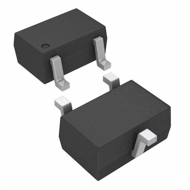
| 供应商器件封装 | 8-SOIC |
| 其它名称 | LT1021DCS810PBF |
| 包装 | 管件 |
| 参考类型 | 串联,旁路,隐埋式齐纳 |
| 安装类型 | 表面贴装 |
| 容差 | ±0.5% |
| 封装/外壳 | 8-SOIC(0.154",3.90mm 宽) |
| 工作温度 | 0°C ~ 70°C |
| 标准包装 | 100 |
| 温度系数 | 20ppm/°C |
| 电压-输入 | 最高 40 V |
| 电压-输出 | 10V |
| 电流-输出 | 10mA |
| 电流-阴极 | - |
| 电流-静态 | 1.7mA |
| 通道数 | 1 |


- 商务部:美国ITC正式对集成电路等产品启动337调查
- 曝三星4nm工艺存在良率问题 高通将骁龙8 Gen1或转产台积电
- 太阳诱电将投资9.5亿元在常州建新厂生产MLCC 预计2023年完工
- 英特尔发布欧洲新工厂建设计划 深化IDM 2.0 战略
- 台积电先进制程称霸业界 有大客户加持明年业绩稳了
- 达到5530亿美元!SIA预计今年全球半导体销售额将创下新高
- 英特尔拟将自动驾驶子公司Mobileye上市 估值或超500亿美元
- 三星加码芯片和SET,合并消费电子和移动部门,撤换高东真等 CEO
- 三星电子宣布重大人事变动 还合并消费电子和移动部门
- 海关总署:前11个月进口集成电路产品价值2.52万亿元 增长14.8%


PDF Datasheet 数据手册内容提取
LT1021 Precision Reference FEATURES DESCRIPTIOU ■ Ultralow Drift: 5ppm/°C Max Slope The LT®1021 is a precision reference with ultralow drift ■ Very Low Noise: <1ppm (0.1Hz to 10Hz) and noise, extremely good long term stability and almost P-P ■ 100% Noise Tested total immunity to input voltage variations. The reference ■ Pin Compatible with Most Bandgap Reference output will both source and sink up to 10mA. Three Applications, Including Ref 01, Ref 02, LM368, voltages are available: 5V, 7V and 10V. The 7V and 10V MC1400 and MC1404 with Greatly Improved units can be used as shunt regulators (two-terminal zeners) Stability, Noise and Drift with the same precision characteristics as the three- ■ Trimmed Output Voltage terminal connection. Special care has been taken to mini- ■ Operates in Series or Shunt Mode mize thermal regulation effects and temperature ■ Output Sinks and Sources in Series Mode induced hysteresis. ■ >100dB Ripple Rejection The LT1021 references are based on a buried zener diode ■ Minimum Input/Output Differential of 1V structure that eliminates noise and stability problems ■ Available in 5-Lead Can, N8 and S8 Packages associated with surface breakdown devices. Further, a subsurface zener exhibits better temperature drift and APPLICATIOUS time stability than even the best bandgap references. Unique circuit design makes the LT1021 the first IC ■ A/D and D/A Converters reference to offer ultralow drift without the use of high ■ Precision Regulators power on-chip heaters. ■ Digital Voltmeters ■ Inertial Navigation Systems The LT1021-7 uses no resistive divider to set output ■ Precision Scales voltage, and therefore exhibits the best long term stability ■ Portable Reference Standard and temperature hysteresis. The LT1021-5 and LT1021- 10 are intended for systems requiring a precise 5V or 10V reference with an initial tolerance as low as ±0.05%. , LTC and LT are registered trademarks of Linear Technology Corporation. All other trademarks are the property of their respective owners. TYPICAL APPLICATIOU Typical Distribution of Temperature Drift 24 Basic Positive and Negative Connections DISTRIBUTION 21 OF THREE RUNS LT1021 LT1021 18 (7 AND 10 ONLY) 15 VIN IN OUT VOUT NC IN OUT %) GND GND S ( 12 T NI –VOUT U 9 R1 = VOUT – (V–) R1 6 ILOAD + 1.5mA 3 –15V (V–) 1021 TA01 – 0 –5 –4 –3 –2 –1 0 1 2 3 4 5 OUTPUT DRIFT (ppm/°C) 1021 TA01 1021fc 1
LT1021 ABSOLUTE WAXIWUW RATIUGS (Note 1) Input Voltage.......................................................... 40V Output Short-Circuit Duration Input/Output Voltage Differential ............................ 35V V = 35V......................................................... 10 sec IN Output-to-Ground Voltage (Shunt Mode Current Limit) V ≤ 20V ................................................... Indefinite IN LT1021-5............................................................. 10V Operating Temperature Range LT1021-7............................................................. 10V Commercial............................................ 0°C to 70°C LT1021-10........................................................... 16V Industrial........................................... –40°C to 85°C Trim Pin-to-Ground Voltage Military............................................ –55°C to 125°C Positive ............................................... Equal to VOUT Storage Temperature Range................ –65°C to 150°C Negative ........................................................... – 20V Lead Temperature (Soldering, 10 sec)................ 300°C PACKAGE/ORDER IUFORWATIOU TOP VIEW TOP VIEW NC* 8 DNC* 1 8 DNC* NC* 1 7 NC* VIN 2 7 DNC* VIN 2 6 VOUT DNC* 3 6 V0UT GND 4 5 TRIM** NC* 3 5 TRIM** 4 N8 PACKAGE S8 PACKAGE GND 8-LEAD PDIP 8-LEAD PLASTIC SO H PACKAGE 8-LEAD TO-5 METAL CAN *CONNECTED INTERNALLY. DO NOT CONNECT EXTERNAL CIRCUITRY TO THESE PINS. **NO TRIM PIN ON LT1021-7. DO NOT CONNECT EXTERNAL CIRCUITRY TO PIN 5 ON LT1021-7 *CONNECTED INTERNALLY. DO NOT CONNECT EXTERNAL CIRCUITRY TO THESE PINS. **NO TRIM PIN ON LT1021-7. DO NOT CONNECT EXTERNAL CIRCUITRY TO PIN 5 ON LT1021-7 TJMAX = 130°C, θJA = 130°C/W (N) TJMAX = 150°C, θJA = 150°C/W,θJC = 45°C/W TJMAX = 130°C, θJA = 150°C/W (S) ORDER PART NUMBER N8 ORDER PART NUMBER LT1021BCH-5 LT1021DCH-5 LT1021BCN8-5 LT1021BMH-5 LT1021DMH-5 LT1021CCN8-5 LT1021CCH-5 LT1021BCH-7 LT1021CIN8-5 LT1021CMH-5 LT1021BMH-7 LT1021DCN8-5 LT1021BMH-10 LT1021DCH-7 LT1021DIN8-5 LT1021DMH-7 LT1021BCN8-7 LT1021BCH-10 LT1021DCN8-7 LT1021CMH-10 LT1021BCN8-10 LT1021DCH-10 LT1021CCN8-10 LT1021DMH-10 LT1021CIN8-10 LT1021DCN8-10 OBSOLETE LT1021DIN8-10 S8 ORDER PART NUMBER S8 PART MARKING LT1021DCS8-5 2105 LT1021DCS8-7 2107 LT1021DCS8-10 2110 Order Options Tape and Reel: Add #TR Lead Free: Add #PBF Lead Free Tape and Reel: Add #TRPBF Lead Free Part Marking: http://www.linear.com/leadfree/ Consult LTC Marketing for parts specified with wider operating temperature ranges. 1021fc 2
LT1021 ELECTRICAL CHARACTERISTICS The ● denotes specifications that apply over the full operating temperature range, otherwise specifications are TA = 25°C. VIN = 10V, IOUT = 0, unless otherwise noted. LT1021-5 PARAMETER CONDITIONS MIN TYP MAX UNITS Output Voltage (Note 2) LT1021C-5 4.9975 5.000 5.0025 V LT1021B-5/LT1021D-5 4.9500 5.000 5.0500 V Output Voltage Temperature Coefficient (Note 3) TMIN ≤ TJ ≤ TMAX LT1021B-5 ● 2 5 ppm/°C LT1021C-5/LT1021D-5 ● 3 20 ppm/°C Line Regulation (Note 4) 7.2V ≤ VIN ≤ 10V 4 12 ppm/V ● 20 ppm/V 10V ≤ VIN ≤ 40V 2 6 ppm/V ● 10 ppm/V Load Regulation (Sourcing Current) 0 ≤ IOUT ≤ 10mA 10 20 ppm/mA (Note 4) ● 35 ppm/mA Load Regulation (Sinking Current) 0 ≤ IOUT ≤ 10mA 60 100 ppm/mA (Note 4) ● 150 ppm/mA Supply Current 0.8 1.2 mA ● 1.5 mA Output Voltage Noise (Note 6) 0.1Hz ≤ f ≤ 10Hz 3.0 µVP-P 10Hz ≤ f ≤ 1kHz 2.2 3.5 µVRMS Long Term Stability of Output Voltage (Note 7) ∆t = 1000Hrs Noncumulative 15 ppm Temperature Hysteresis of Output ∆T = ±25°C 10 ppm The ● denotes specifications that apply over the full operating temperature range, otherwise specifications are TA = 25°C. V = 12V, I = 0, unless otherwise noted. IN OUT LT1021-7 PARAMETER CONDITIONS MIN TYP MAX UNITS Output Voltage (Note 2) 6.95 7.00 7.05 V Output Voltage Temperature Coefficient (Note 3) TMIN ≤ TJ ≤ TMAX LT1021B-7 ● 2 5 ppm/°C LT1021D-7 ● 3 20 ppm/°C Line Regulation (Note 4) 8.5V ≤ VIN ≤ 12V 1.0 4 ppm/V ● 2.0 8 ppm/V 12V ≤ VIN ≤ 40V 0.5 2 ppm/V ● 1.0 4 ppm/V Load Regulation (Sourcing Current) 0 ≤ IOUT ≤ 10mA 12 25 ppm/mA (Note 4) ● 40 ppm/mA Load Regulation (Shunt Mode) 1.2mA ≤ ISHUNT ≤ 10mA 50 100 ppm/mA (Notes 4, 5) ● 150 ppm/mA Supply Current (Series Mode) 0.75 1.2 mA ● 1.5 mA Minimum Current (Shunt Mode) V is Open 0.7 1.0 mA IN ● 1.2 mA Output Voltage Noise (Note 6) 0.1Hz ≤ f ≤ 10Hz 4.0 µVP-P 10Hz ≤ f ≤ 1kHz 2.5 4.0 µVRMS Long Term Stability of Output Voltage (Note 7) ∆t = 1000Hrs Noncumulative 7 ppm Temperature Hysteresis of Output ∆T = ±25°C 3 ppm 1021fc 3
LT1021 ELECTRICAL CHARACTERISTICS The ● denotes specifications that apply over the full operating temperature range, otherwise specifications are TA = 25°C. VIN = 15V, IOUT = 0, unless otherwise noted. LT1021-10 PARAMETER CONDITIONS MIN TYP MAX UNITS Output Voltage (Note 2) LT1021C-10 9.995 10.00 10.005 V LT1021B-10/LT1021D-10 9.950 10.00 10.050 V Output Voltage Temperature Coefficient (Note 3) TMIN ≤ TJ ≤ TMAX LT1021B-10 ● 2 5 ppm/°C LT1021C-10/LT1021D-10 ● 5 20 ppm/°C Line Regulation (Note 4) 11.5V ≤ VIN ≤ 14.5V 1.0 4 ppm/V ● 6 ppm/V 14.5V ≤ VIN ≤ 40V 0.5 2 ppm/V ● 4 ppm/V Load Regulation (Sourcing Current) 0 ≤ IOUT ≤ 10mA 12 25 ppm/mA (Note 4) ● 40 ppm/mA Load Regulation (Shunt Mode) 1.7mA ≤ ISHUNT ≤ 10mA 50 100 ppm/mA (Notes 4, 5) ● 150 ppm/mA Supply Current (Series Mode) 1.2 1.7 mA ● 2.0 mA Minimum Current (Shunt Mode) V is Open 1.1 1.5 mA IN ● 1.7 mA Output Voltage Noise (Note 6) 0.1Hz ≤ f ≤ 10Hz 6.0 µVP-P 10Hz ≤ f ≤ 1kHz 3.5 6 µVRMS Long Term Stability of Output Voltage (Note 7) ∆t = 1000Hrs Noncumulative 15 ppm Temperature Hysteresis of Output ∆T = ±25°C 5 ppm Note 1: Absolute Maximum Ratings are those values beyond which the life Note 5: Shunt mode regulation is measured with the input open. With the of a device may be impaired. input connected, shunt mode current can be reduced to 0mA. Load Note 2: Output voltage is measured immediately after turn-on. Changes regulation will remain the same. due to chip warm-up are typically less than 0.005%. Note 6: RMS noise is measured with a 2-pole highpass filter at 10Hz and a Note 3: Temperature coefficient is measured by dividing the change in 2-pole lowpass filter at 1kHz. The resulting output is full-wave rectified and output voltage over the temperature range by the change in temperature. then integrated for a fixed period, making the final reading an average as Separate tests are done for hot and cold; TMIN to 25°C and 25°C to TMAX. opposed to RMS. Correction factors are used to convert from average to Incremental slope is also measured at 25°C. RMS and correct for the non-ideal bandpass of the filters. Note 4: Line and load regulation are measured on a pulse basis. Output Peak-to-peak noise is measured with a single highpass filter at 0.1Hz and a changes due to die temperature change must be taken into account 2-pole lowpass filter at 10Hz. The unit is enclosed in a still-air environment separately. Package thermal resistance is 150°C/W for TO-5 (H), 130°C/W to eliminate thermocouple effects on the leads. Test time is 10 seconds. for N and 150°C/W for the SO-8. Note 7: Consult factory for units with long term stability data. 1021fc 4
LT1021 TYPICAL PERFORWAUCE CHARACTERISTICS Minimum Input/Output Differential Ripple Rejection Ripple Rejection LT1021-7, LT1021-10 115 130 1.6 f = 150Hz LT1021-7 VIN = 15V TJ = 125 °C 120 COUT = 0 1.4 110 LT1021-10 110 LT1021-7 E (V) 1.2 TJ = –55 °C G N (dB)105 N (dB) 100 LT1021-10 VOLTA 1.0 TJ = 25 °C CTIO100 LT1021-5 CTIO 90 LT1021-5 PUT 0.8 REJE 95 REJE 80 T/OUT 0.6 70 PU 0.4 N 90 I 60 0.2 85 50 0 0 5 10 15 20 25 30 35 40 10 100 1k 10k 0 2 4 6 8 10 12 14 16 18 20 INPUT VOLTAGE (V) FREQUENCY (Hz) OUTPUT CURRENT (mA) LT1021 G01 LT1021 G02 1021 G03 Start-Up (Shunt Mode) Start-Up (Series Mode) LT1021-7, LT1021-10 Output Voltage Noise Spectrum 13 11 400 VIN = 0V TO 12V 12 LT1021-10 350 10 11 OLTAGE (V) 1980 LT1021-10 OLTAGE (V) 89 0VVOUT + 2VNC 1kINGO NUDT VOUT AGE (nV/Hz)√223050000 OUTPUT V 67 LLTT11002211--57 OUTPUT V 7 LT1021-7 NOISE VOLT110500 LLTT11002211--170 5 6 50 LT1021-5 4 3 5 0 0 2 4 6 8 10 12 14 0 2 4 6 8 10 12 10 100 1k 10k TIME (µs) TIME (µs) FREQUENCY (Hz) LT1021 G04 LT1021 G05 LT1021 G06 Output Voltage Temperature Drift Output Voltage Noise LT1021-5 Load Regulation LT1021-5 16 5.006 5 COUT = 0 VIN = 8V FILTER = 1 POLE 4 14 fLOW = 0.1Hz 5.004 3 12 E (V)µ 10 TAGE (V)5.002 NGE (mV) 21 RMS NOIS 68 LTL1T012012-110-7 UTPUT VOL 54..090908 UTPUT CHA ––021 4 O O LT1021-5 4.996 –3 2 –4 0 4.994 –5 10 100 1k 10k –50 –25 0 25 50 75 100 125 –10 –8 –6 –4 –2 0 2 4 6 8 10 BANDWIDTH (Hz) TEMPERATURE (°C) SOURCING SINKING LT1021 G07 LT1021 G08 OUTPUT CURRENT (mA) LT1021 G09 1021fc 5
LT1021 TYPICAL PERFORWAUCE CHARACTERISTICS Sink Mode* Current Limit Quiescent Current LT1021-5 LT1021-5 Thermal Regulation LT1021-5 1.8 60 IOUT = 0 VIN = 8V VIN = 25V 1.6 ∆POWER = 200mW 50 PUT CURRENT (mA) 01110.....80246 TTTJJJ === –1225555°°C°CC ENT INTO OUTPUT (mA) 423000 UTPUT CHANGE (mV) ––10..050 LROEAGDULATION TRHEEGRUMLAATLI ON N R O I 0.4 CUR 10 ILOAD = 10mA 0.2 0 0 0 5 10 15 20 25 30 35 40 0 2 4 6 8 10 12 14 16 18 0 20 40 60 80 100 120 140 INPUT VOLTAGE (V) OUTPUT VOLTAGE (V) TIME (ms) LT1021 G10 *NOTE THAT AN INPUT VOLTAGE IS REQUIRED LT1021 G12 FOR 5V UNITS. LT1021 G11 Load Transient Response Load Transient Response Output Noise 0.1Hz to 10Hz LT1021-5, C = 0 LT1021-5, C = 1000pF LT1021-5 LOAD LOAD ISOURCE = 0 ISINK = 0 FILTERING = 1 ZERO AT 0.1Hz E (50mV/DIV) ISOURCE 5=0 0mV ISINK5 =0 m0V E (20mV/DIV) 20mV 20mV NOISE (5V/DIV)µ 5µV (1pp2m P)OLES AT 10Hz CHANG ISOURCE = 0.5mA ISINK = 0.2mA CHANG ISOURCE = 0.2mA ISINK = 0.2mA LTAGE TPUT ISOURCE = 2-10mA ISINK = 2-10mA TPUT ISOURCE = 2-10mA ISINK = 2-10mA UT VO U U P O O T U O ∆ISOURCE = 100µAP-P ∆ISINK = 100µAP-P ∆ISOURCE = 100µAP-P ∆ISINK = 100µAP-P 0 1 2 3 4 0 1 2 3 4 0 5 10 15 20 0 5 10 15 20 0 1 2 3 4 5 6 TIME (µs) TIME (µs) TIME (MINUTES) LT1021 G13 LT1021 G14 LT1021 G15 Output Voltage Temperature Load Regulation Drift LT1021-7 LT1021-7, LT1021-10 Quiescent Current LT1021-7 7.003 5 1.8 VIN = 12V IOUT = 0 4 1.6 7.002 3 1.4 OUTPUT VOLTAGE (V)776...009009109 OUTPUT CHANGE (mV) –––320211 INPUT CURRENT (mA) 01010.....80426 TTTJJJ === 2–1525°55C°°CC 6.998 –4 0.2 6.997 –5 0 –50 –25 0 25 50 75 100 125 –10 –8 –6 –4 –2 0 2 4 6 8 10 0 5 10 15 20 25 30 35 40 TEMPERATURE (°C) SOURCING SINKING INPUT VOLTAGE (V) LT1021 G16 OUTPUT CURRENT (mA) LT1021 G17 LT1021 G18 1021fc 6
LT1021 TYPICAL PERFORWAUCE CHARACTERISTICS Shunt Mode Current Limit Shunt Characteristics LT1021-7 LT1021-7 Thermal Regulation LT1021-7 1.2 60 INPUT PIN OPEN INPUT PIN OPEN VIN = 27V ∆POWER = 200mW 1.0 50 A) A) LOAD TPUT (m 0.8 TJ = –55°C TPUT (m 40 GE (mV) –0.50 REGULATION OU TJ = 25°C OU AN THERMAL NTO 0.6 NTO 30 T CH –1.0 REGULATION* T I T I PU –1.5 N 0.4 N 20 T E E U R R O R R CU 0.2 TJ = 125°C CU 10 ILOAD = 10mA 0 0 0 1 2 3 4 5 6 7 8 9 0 2 4 6 8 10 12 14 16 18 0 20 40 60 80 100 120 140 OUTPUT TO GROUND VOLTAGE (V) OUTPUT VOLTAGE (V) TIME (ms) 1021 G19 LT1021 G20 *INDEPENDENT OF TEMPERATURE COEFFICIENT LT1021 G21 Load Transient Response Load Transient Response Output Noise 0.1Hz to 10Hz LT1021-7, C = 0 LT1021-7, C = 1000pF LT1021-7 LOAD LOAD ISINK = 0.8mA ISOURCE = 0 ISINK = 0.6mA FILTERING = 1 ZERO AT 0.1Hz ISOURCE = 0 DIV) 2 POLES AT 10Hz HANGE 5mV ISINK = 1.2mA HANGE 5mV 20mV E (5V/µ 5µV (0.7ppm) C C S E E OI G 50mV G N OLTA ISOURCE = 0.5mA OLTA ISOURCE = 0.5mA ISINK = 0.8mA AGE UTPUT V ISINK = 1.4mA UTPUT V ISINK = 1mA UT VOLT O O TP ISOURCE = 2-10mA ISINK = 2-10mA ISOURCE = 2-10mA ISINK = 2-10mA OU ∆ISOURCE = 100µAP-P ∆ISINK = 100µAP-P ∆ISOURCE = 100µAP-P ∆ISINK = 100µAP-P 0 1 2 3 4 0 1 2 3 4 0 5 10 15 20 0 5 10 15 20 0 1 2 3 4 5 6 TIME (µs) 5µs/DIV TIME (MINUTES) NOTE VERTICAL SCALE CHANGE NOTE VERTICAL SCALE CHANGE LT1021 G24 BETWEEN SOURCING AND SINKING BETWEEN SOURCING AND SINKING LT1021 G22 LT1021 G23 Output Voltage Temperature Load Regulation Drift LT1021-10 LT1021-7, LT1021-10 Input Supply Current LT1021-10 10.006 5 1.8 4 VIN = 12V 1.6 IOUT = 0 TJ = –55°C 10.004 3 OUTPUT VOLTAGE (V)11009...009009208 OUTPUT CHANGE (mV) ––20211 INPUT CURRENT (mA) 010110......480246 TTJJ = = 1 2255°°CC –3 9.996 –4 0.2 9.994 –5 0 –50 –25 0 25 50 75 100 125 –10 –8 –6 –4 –2 0 2 4 6 8 10 0 5 10 15 20 25 30 35 40 TEMPERATURE (°C) SOURCING SINKING INPUT VOLTAGE (V) LT1021 G25 OUTPUT CURRENT (mA) 1021 G26 1021 G27 1021fc 7
LT1021 TYPICAL PERFORWAUCE CHARACTERISTICS Shunt Mode Current Limit Shunt Characteristics LT1021-10 LT1021-10 Thermal Regulation LT1021-10 1.8 60 INPUT PIN OPEN INPUT PIN OPEN VIN = 30V 1.6 ∆POWER = 200mW 50 A) 1.4 A) LOAD PUT (m 1.2 PUT (m 40 E (mV) –0.50 REGULATION T T G OU 1.0 TJ = –55°C OU AN NTO 0.8 NTO 30 T CH –1.0 TRHEEGRUMLAATLI ON* ENT I 0.6 TJ = 25°C ENT I 20 UTPU –1.5 R R O CUR 0.4 TJ = 125°C CUR 10 ILOAD = 10mA 0.2 0 0 0 2 4 6 8 10 12 0 2 4 6 8 10 12 14 16 18 0 20 40 60 80 100 120 140 OUTPUT TO GROUND VOLTAGE (V) OUTPUT VOLTAGE (V) TIME (ms) 1021 G28 1021 G29 *INDEPENDENT OF TEMPERATURE COEFFICIENT 1021 G30 Load Transient Response Load Transient Response Output Noise 0.1Hz to 10Hz LT1021-10, C = 0 LT1021-10, C = 1000pF LT1021-10 LOAD LOAD ISINK = 0.6mA ISINK = 0.8mA FILTERING = 1 ZERO AT 0.1Hz ISOURCE = 0 ISOURCE = 0 DIV) 2 POLES AT 10Hz GE 50mV GE 20mV V/µ N N 0 10µV (1ppm) UTPUT VOLTAGE CHA ISOU1R0CmEV = 0.2mA IISSIINNKK == 10m.8AmA UTPUT VOLTAGE CHA ISOU5RmCVE = 0.5mAISINK = 1.2mAISINK = 1.4mA UT VOLTAGE NOISE (1 O O P ISOURCE = 2-10mA ISINK = 2-10mA ISOURCE = 2-10mA ISINK = 2-10mA OUT ∆ISOURCE = 100µAP-P ∆ISINK = 100µAP-P ∆ISOURCE = 100µAP-P ∆ISINK = 100µAP-P 0 1 2 3 4 0 1 2 3 4 0 1 2 3 4 0 1 2 3 4 0 1 2 3 4 5 6 TIME (µs) TIME (µs) TIME (MINUTES) NOTE VERTICAL SCALE CHANGE NOTE VERTICAL SCALE CHANGE 1021 G33 BETWEEN SOURCING AND SINKING BETWEEN SOURCING AND SINKING 1021 G31 1021 G32 1021fc 8
LT1021 APPLICATIOUNS INUFORWMATIOUN Effect of Reference Drift on System Accuracy The LT1021-10 “C” version is pre-trimmed to ±5mV and therefore can utilize a restricted trim range. A 75k resistor A large portion of the temperature drift error budget in in series with a 20kΩ potentiometer will give ±10mV trim many systems is the system reference voltage. This graph range. Effect on the output TC will be only 1ppm/°C for the indicates the maximum temperature coefficient allowable ±5mV trim needed to set the “C” device to 10.000V. if the reference is to contribute no more than 0.5LSB error to the overall system performance. The example shown is LT1021-5 a 12-bit system designed to operate over a temperature range from 25°C to 65°C. Assuming the system calibra- The LT1021-5 does have an output voltage trim pin, but tion is performed at 25°C, the temperature span is 40°C. the TC of the nominal 4V open-circuit voltage at this pin is It can be seen from the graph that the temperature coeffi- about –1.7mV/°C. For the voltage trimming not to affect cient of the reference must be no worse than 3ppm/°C if reference output TC, the external trim voltage must track it is to contribute less than 0.5LSB error. For this reason, the voltage on the trim pin. Input impedance of the trim pin the LT1021 family has been optimized for low drift. is about 100kΩ and attenuation to the output is 13:1. The technique shown below is suggested for trimming the Maximum Allowable Reference Drift output of the LT1021-5 while maintaining minimum shift in output temperature coefficient. The R1/R2 ratio is 100 R chosen to minimize interaction of trimming and TC shifts, O F NT 8-BIT so the exact values shown should be used. E EFFICIm/C)° URE COOR (pp 10 10-BIT LT1021-5 TR AR UM TEMPER0.5LSB E 14-BIT 12-BIT ING ND TROIUMT R271k R2VOUT M 50k XI 1N4148 A M 1.0 0 10 20 30 40 50 60 70 80 90 100 TEMPERATURE SPAN (°C) 1021 AI02 LT1021 AI01 LT1021-7 Trimming Output Voltage The 7V version of the LT1021 has no trim pin because the internal architecture does not have a point which could be LT1021-10 driven conveniently from the output. Trimming must therefore be done externally, as is the case with ordinary The LT1021-10 has a trim pin for adjusting output voltage. reference diodes. Unlike these diodes, however, the out- The impedance of the trim pin is about 12kΩ with a put of the LT1021 can be loaded with a trim potentiometer. nominal open-circuit voltage of 5V. It is designed to be The following trim techniques are suggested; one for driven from a source impedance of 3kΩ or less to mini- voltage output and one for current output. The voltage mize changes in the LT1021 TC with output trimming. output is trimmed for 6.95V. Current output is 1mA, as Attenuation between the trim pin and the output is 70:1. shown, into a summing junction, but all resistors may be This allows ±70mV trim range when the trim pin is tied to scaled for currents up to 10mA. the wiper of a potentiometer connected between the output and ground. A 10kΩ potentiometer is recom- Both of these circuits use the trimmers in a true potentio- mended, preferably a 20 turn cermet type with stable metric mode to reduce the effects of trimmer TC. The characteristics over time and temperature. voltage output has a 200Ω impedance, so loading must be 1021fc 9
LT1021 APPLICATIOUNS INUFORWMATIOUN minimized. In the current output circuit, R1 determines Kelvin Connections output current. It should have a TC commensurate with the Although the LT1021 does not have true force/sense LT1021 or track closely with the feedback resistor around capability at its outputs, significant improvements in ground the op amp. loop and line loss problems can be achieved with proper hook-up. In series mode operation, the ground pin of the LT1021 carries only ≈1mA and can be used as a sense LT1021-7 line, greatly reducing ground loop and loss problems on IN OUT the low side of the reference. The high side supplies load GND R2* R1* 14k 200Ω current so line resistance must be kept low. Twelve feet of 1% 1% R3 VOUT #22 gauge hook-up wire or 1 foot of 0.025 inch printed 10k 6.950V circuit trace will create 2mV loss at 10mA output current. TC TRACKING TO 50ppm/°C This is equivalent to 1LSB in a 10V, 12-bit system. 1021 AI03 The following circuits show proper hook-up to minimize errors due to ground loops and line losses. Losses in the LT1021-7 output lead can be greatly reduced by adding a PNP boost IN OUT GND R1* transistor if load currents are 5mA or higher. R2 can be R2** 7.15k added to further reduce current in the output sense lead. 182k R3 50k 1.000mA Standard Series Mode – OP AMP LT1021 + KEEP THIS LINE RESISTANCE LOW INPUT IN OUT 1021 AI04 + GND LOAD *RESISTOR TC DETERMINES IOUT TC **TC ≤ (10 • R1) TC. R2 AND R3 SCALE WITH R1 FOR DIFFERENT OUTPUT CURRENTS GROUND RETURN 1021 AI05 Capacitive Loading and Transient Response The LT1021 is stable with all capacitive loads, but for Series Mode with Boost Transistor optimum settling with load transients, output capacitance should be under 1000pF. The output stage of the reference is class AB with a fairly low idling current. This makes INPUT R1 transient response worst-case at light load currents. Be- 220Ω cause of internal current drain on the output, actual worst- 2N3906 case occurs at I = 0 on LT1021-5, I = LOAD LOAD –0.8mA (sinking) on LT1021-7 and I = 1.4mA (sink- IN LOAD LT1021 ing) on LT1021-10. Significantly better load transient OUT response is obtained by moving slightly away from these GND LOAD R2* points. See Load Transient Response curves for details. In general, best transient response is obtained when the output is sourcing current. In critical applications, a 10µF GROUND RETURN 1021 AI06 solid tantalum capacitor with several ohms in series *OPTIONAL—REDUCES CURRENT IN OUTPUT SENSE LEAD provides optimum output bypass. R2 = 2.4k (LT1021-5), 3k (LT1021-7), 5.6k (LT1021-10) 1021fc 10
LT1021 APPLICATIOUNS INUFORWMATIOUN Effects of Air Movement on Low Frequency Noise copper lead frames used on dual-in-line packages are not nearly as sensitive to thermally generated noise because The LT1021 has very low noise because of the buried zener they are intrinsically matched. used in its design. In the 0.1Hz to 10Hz band, peak-to-peak noise is about 0.5ppm of the DC output. To achieve this There is nothing magical about foam cups—any enclo- low noise, however, care must be taken to shield the sure which blocks air flow from the reference will do. reference from ambient air turbulence. Air movement can Smaller enclosures are better since they do not allow the create noise because of thermoelectric differences build-up of internally generated air movement. Naturally, between IC package leads (especially kovar lead TO-5) and heat generating components external to the reference printed circuit board materials and/or sockets. Power itself should not be included inside the enclosure. dissipation in the reference, even though it rarely exceeds 20mW, is enough to cause small temperature gradients in Noise Induced By Air Turbulence (TO-5 Package) the package leads. Variations in thermal resistance, caused by uneven air flow, create differential lead temperatures, LT1021-7 (TO-5 PACKAGE) thereby causing thermoelectric voltage noise at the output V) f = 0.01Hz TO 10Hz DI of the reference. The following XY plotter trace dramati- V/ µ 20 20µV cally illustrates this effect. The first half of the plot was E ( FOAM CUP S REMOVED done with the LT1021 shielded from ambient air with a OI N E small foam cup. The cup was then removed for the second G A T L half of the trace. Ambient in both cases was a lab environ- O V T ment with no excessive air turbulence from air condition- U P T ers, opening/closing doors, etc. Removing the foam cup OU increases the output noise by almost an order of magni- 0 2 4 6 8 10 12 tude in the 0.01Hz to 1Hz band! The kovar leads of the TIME (MINUTES) TO-5 (H) package are the primary culprit. Alloy 42 and 1021 AI07 TYPICAL APPLICATIONUS Restricted Trim Range for Improved Resolution, 10V, “C” Version Only LT1021-10 Full Trim Range (±0.7%) Negative Series Reference 15V LT1021C-10 LT1021-10 R1 VIN IN OUT 10.000V VIN IN OUT VOUT 4.7k LT1021-10 GND TRIM GND TRIM IN OUT R1 D1 75k R1* R2 15V GND R2 10k 4.7k 50k –15V –10V AT 50mA TRIM RANGE ≈ ±10mV 1021 TA11 *CAN BE RAISED TO 20k 1F02O1 RTA03 2NQ21905 LT1021 TA04 LESS CRITICAL APPLICATIONS 1021fc 11
LT1021 TYPICAL APPLICATIONUS Boosted Output Current Boosted Output Current with No Current Limit with Current Limit Ultraprecise Current Source V+ ≥ (VOUT + 1.8V) V+ ≥ VOUT + 2.8V R2210Ω DLE1D* R2210Ω 8.2Ω LT1021-7 15V IN OUT 2N2905 GND 17.4k 2N2905 1% IN TRIM LT1021 IN 100Ω OUT 10V AT LT1021 6.98k* 100mA 10V AT 0.1% GND + 2µF OUT 100mA 15V STAONLITD GND + 2µF 7 – 2 *LOW TC SOLID 6 TANT LT1001 3 1021 TA05 + 1021 TA06 4 *GLOWS IN CURRENT LIMIT, –15V IOUT = 1mA DO NOT OMIT REGULATION < 1ppm/V COMPLIANCE = –13V TO 7V 1021 TA07 2-Pole Lowpass Filtered Reference Operating 5V Reference from 5V Supply 5V LOGIC SUPPLY M1YµLFAR VIN CMOS LOGIC GATE** 1N914 LT1021-5 – + 1N914 ≈8.5V 5V fIN ≥ 2kHz* IN OUT REFERENCE LT1021 LT1001 VREF C1* + VIN IN OUT + 5µF C5µ2*F GND R1 R2 GND 36k 36k 0.5µF TOTAL NOISE f = 10Hz MYLAR ≤2µVRMS *FOR HIGHER FREQUENCIES C1 AND C2 MAY BE DECREASED 1Hz ≤ f ≤ 10kHz **PARALLEL GATES FOR HIGHER REFERENCE CURRENT LOADING 1021 TA16 –VREF 1021 TA13 Trimming 10V Units to 10.24V CMOS DAC with Low Drift Full-Scale Trimming** LT1021-10 R3 VIN IN OUT VOUT = 10.24V OUT 4.02K 1% TRIM GND LT1021-10 R4* 100Ω TRIM FB FULL-SCALE GND R1 CMOS 30pF ADJUST 4.99k DAC IOUT – 4.32k 1% 7520, ETC REF LT1007C 10V 5k F.S. R2 + 40.2Ω 1% V– = –15V* 1.2k *TC LESS THAN 200ppm/°C *MUST BE WELL REGULATED **NO ZERO ADJUST REQUIRED dVOUT=15mV –15V WITH LT1007 (V0S ≤ 60µV) LT1236 TA15 dV– V 1021 TA12 1021fc 12
LT1021 TYPICAL APPLICATIONUS Strain Gauge Conditioner for 350Ω Bridge Negative Shunt Reference Driven by Current Source R1 357Ω 1/2W LT1021-10 OUT 28mA LT1021-10 28.5mA GND 15V IN OUT 5V 350Ω STRAIN R3 –10V (ILOAD ≤ 1mA) GND GAUGE BRIDGE** 2M 2.5mA R2 + 3 20k 2 – LM334 6 LM301A† R4 LT1012C 6 VOUT 2 20k 3 ×100 1 – + R5 27Ω 100pF 8 2M R6* 2M –11V TO –40V 1021 TA14 –5V 1021 TA09 357Ω 1/2W –15V *THIS RESISTOR PROVIDES POSITIVE FEEDBACK TO **BRIDGE IS ULTRALINEAR WHEN ALL LEGS ARE THE BRIDGE TO ELIMINATE LOADING EFFECT OF ACTIVE, TWO IN COMPRESSION AND TWO IN TENSION, THE AMPLIFIER. EFFECTIVE ZIN OF AMPLIFIER OR WHEN ONE SIDE IS ACTIVE WITH ONE COMPRESSED STAGE IS ≥1MΩ. IF R2 TO R5 ARE CHANGED, AND ONE TENSIONED LEG SET R6 = R3 †OFFSET AND DRIFT OF LM301A ARE VIRTUALLY ELIMINATED BY DIFFERENTIAL CONNECTION OF LT1012C Precision DAC Reference with System TC Trim Handling Higher Load Currents 15V 30mA LT1021-10 15V IN OUT 8.87k IN R1* GND 1% LT1021-10 169Ω OUT VOUT 50k 10V D1 ROOM TEMP GND 1N457 10k TRIM 1.24k TC 5T0RkI M* 1% 110%.36k RL TCYUPRIRCEANLT L =O A3D0mA 1% 10k D2 200k 1021 TA08 1% 1N457 1% *SELECT R1 TO DELIVER TYPICAL LOAD CURRENT. LT1021 WILL THEN SOURCE OR SINK AS NECESSARY TO MAINTAIN PROPER OUTPUT. DO NOT REMOVE LOAD 50k 1mA 8.45k AS OUTPUT WILL BE DRIVEN UNREGULATED HIGH. LINE REGULATION IS DEGRADED IN THIS APPLICATION *TRIMS 1mA REFERENCE CURRENT DAC TC BY ±40ppm/°C. THIS TRIM SCHEME HAS VERY LITTLE EFFECT ON ROOM TEMPERATURE CURRENT TO MINIMIZE ITERATIVE TRIMMING 1021 TA17 1021fc 13
LT1021 TYPICAL APPLICATIONUS Ultralinear Platinum Temperature Sensor* LT1021-10 OUT IN 20V R2* GND R10 5k 182k 1% R1** R14 253k 5k R11 6.65M R15 1% 10k R8 RF** 10M 654k R9 R12 100k 1k R13 20V 24.3k R5 2 – 7 R5k3** 41.R7%45k 210%0k 3 +LT1001 6 V–O5U0T°C = 1≤0 T0 m≤ V1/5°0C°C 4 RS† 100Ω AT R6 –15V 0°C 619k †STANDARD INDUSTRIAL 100Ω PLATINUM 4-WIRE SENSOR, 1% ROSEMOUNT 78S OR EQUIVALENT. α = 0.00385 R319%72k TTTRRRIIIMMM RRR911 24F OFFOORRR V VVOOOUUUT TT= == 0 15V0V AV AT AT 0T 5° C10°0C0°C –15V USE TRIM SEQUENCE AS SHOWN. TRIMS ARE NONINTERACTIVE SO THAT ONLY ONE TRIM SEQUENCE IS NORMALLY REQUIRED. *FEEDBACK LINEARIZES OUTPUT TO ±0.005°C FROM –50°C TO 150°C **WIREWOUND RESISTORS WITH LOW TC 1021 TA10 EQUIVALEU T SCHEW ATIC INPUT Q3 D1 D2 OUTPUT D3 R1 Q1 – + A1 R2 D4 6.3V Q2 GND LT1021 ES 1021fc 14
LT1021 PACKAGE DESCRIPTIOUN H Package 8-Lead TO-5 Metal Can (.200 Inch PCD) (Reference LTC DWG # 05-08-1320) .335 – .370 (8.509 – 9.398) DIA .305 – .335 (7.747 – 8.509) .040 (1.016) .050 MAX (1.270) .165 – .185 MAX (4.191 – 4.699) REFERENCE SEATING PLANE PLANE GPLAAUNGEE .500 – .750 .010 – .045* (12.700 – 19.050) (0.254 – 1.143) .016 – .021** (0.406 – 0.533) .027 – .045 (0.686 – 1.143) 45° PIN 1 .028 – .034 (0.711 – 0.864) .200 (5.080) TYP .110 – .160 (2.794 – 4.064) INSULATING STANDOFF *LEAD DIAMETER IS UNCONTROLLED BETWEEN THE REFERENCE PLANE AND THE SEATING PLANE .016 – .024 **FOR SOLDER DIP LEAD FINISH, LEAD DIAMETER IS (0.406 – 0.610) H8(TO-5) 0.200 PCD 0204 N8 Package 8-Lead PDIP (Narrow .300 Inch) (Reference LTC DWG # 05-08-1510) .400* (10.160) MAX 8 7 6 5 .255 ± .015* (6.477 ± 0.381) 1 2 3 4 .300 – .325 .045 – .065 .130 ± .005 (7.620 – 8.255) (1.143 – 1.651) (3.302 ± 0.127) .065 (1.651) .008 – .015 TYP (0.203 – 0.381) .120 (3.048) .020 (8..322555–++–00..00..8331885591) (.2B1.S05C04) (0..041587 ±± .00M.00I37N6) (0MN.85 I10N0082) NOTE: INCHES 1. DIMENSIONS ARE MILLIMETERS *THESE DIMENSIONS DO NOT INCLUDE MOLD FLASH OR PROTRUSIONS. MOLD FLASH OR PROTRUSIONS SHALL NOT EXCEED .010 INCH (0.254mm) 1021fc Information furnished by Linear Technology Corporation is believed to be accurate and reliable. 15 However, no responsibility is assumed for its use. Linear Technology Corporation makes no represen- tation that the interconnection of its circuits as described herein will not infringe on existing patent rights.
LT1021 PACKAGE DESCRIPTIOUN S8 Package 8-Lead Plastic Small Outline (Narrow .150 Inch) (Reference LTC DWG # 05-08-1610) .189 – .197 .045 ±.005 (4.801 – 5.004) .050 BSC NOTE 3 8 7 6 5 .245 MIN .160 ±.005 .150 – .157 .228 – .244 (3.810 – 3.988) (5.791 – 6.197) NOTE 3 .030 ±.005 TYP 1 2 3 4 RECOMMENDED SOLDER PAD LAYOUT .010 – .020 × 45°(cid:31) .053 – .069 (0.254 – 0.508) (1.346 – 1.752) .004 – .010 .008 – .010 (0.203 – 0.254) 0°– 8° TYP (0.101 – 0.254) .016 – .050 .014 – .019 .050 (0.406 – 1.270) (0.355 – 0.483) (1.270) NOTE: INCHES TYP BSC 1. DIMENSIONS IN (MILLIMETERS) 2. DRAWING NOT TO SCALE 3. THESE DIMENSIONS DO NOT INCLUDE MOLD FLASH OR PROTRUSIONS. MOLD FLASH OR PROTRUSIONS SHALL NOT EXCEED .006" (0.15mm) SO8 0303 RELATED PARTS PART NUMBER DESCRIPTION COMMENTS LT1019 Precision Bandgap Reference 0.05%, 5ppm/°C LT1027 Precision 5V Reference 0.02%, 2ppm/°C LT1236 Precision Reference SO-8, 5V and 10V, 0.05%, 5ppm/°C LTC®1258 Micropower Reference 200mV Dropout, MSOP LT1389 Nanopower Shunt Reference 800nA Operating Current LT1460 Micropower Reference SOT-23, 2.5V, 5V, 10V LT1634 Micropower Shunt Reference 0.05%, 10ppm/°C, MSOP 1021fc 16 Linear Technology Corporation LT 1005 REV C • PRINTED IN USA 1630 McCarthy Blvd., Milpitas, CA 95035-7417 (408) 432-1900 ● FAX: (408) 434-0507 ● www.linear.com © LINEAR TECHNOLOGY CORPORATION 1995
Mouser Electronics Authorized Distributor Click to View Pricing, Inventory, Delivery & Lifecycle Information: A nalog Devices Inc.: LT1021CIN8-5#PBF LT1021DCN8-7 LT1021DCS8-7#TRPBF LT1021DCS8-10#PBF LT1021CCN8-5#PBF LT1021BMH-5 LT1021CCN8-10 LT1021DCS8-5 LT1021DIN8-5 LT1021BCN8-5 LT1021DCN8-10 LT1021CCN8- 10#PBF LT1021BCN8-7 LT1021DCS8-10#TR LT1021BCN8-7#PBF LT1021DIN8-10 LT1021DCS8-5#PBF LT1021DCS8-7 LT1021DIN8-5#PBF LT1021CIN8-10#PBF LT1021DCN8-10#PBF LT1021DCS8-5#TR LT1021CCN8-5 LT1021CIN8-10 LT1021DCN8-5 LT1021BCH-5 LT1021DCS8-7#PBF LT1021CIN8-5 LT1021CMH- 5 LT1021DCS8-5#TRPBF LT1021DCN8-5#PBF LT1021DCS8-10 LT1021BCN8-10 LT1021DCS8-7#TR LT1021DCS8-10#TRPBF LT1021DIN8-10#PBF LT1021BCN8-5#PBF LT1021DCN8-7#PBF LT1021BCN8-10#PBF LT1021CCH-5 LT1021BMH-10