 Datasheet下载
- 型号: LPS331APTR
- 制造商: STMicroelectronics
- 库位|库存: xxxx|xxxx
- 要求:
| 数量阶梯 | 香港交货 | 国内含税 |
| +xxxx | $xxxx | ¥xxxx |
查看当月历史价格
查看今年历史价格
LPS331APTR产品简介:
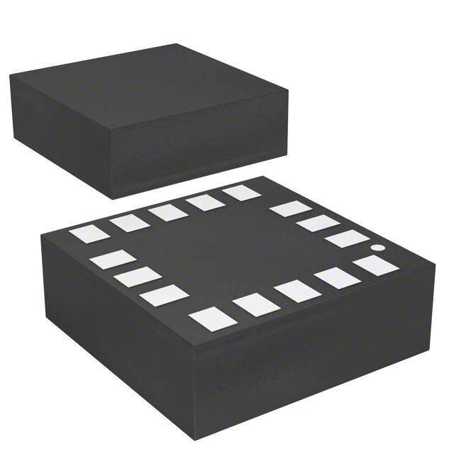
ICGOO电子元器件商城为您提供LPS331APTR由STMicroelectronics设计生产,在icgoo商城现货销售,并且可以通过原厂、代理商等渠道进行代购。 LPS331APTR价格参考¥29.07-¥32.70。STMicroelectronicsLPS331APTR封装/规格:压力传感器,变送器, 绝对 压力 传感器 3.77 PSI ~ 18.27 PSI(26 kPa ~ 126 kPa) 24 b 16-VFLGA。您可以下载LPS331APTR参考资料、Datasheet数据手册功能说明书,资料中有LPS331APTR 详细功能的应用电路图电压和使用方法及教程。
STMicroelectronics的LPS331APTR是一款高性能压阻式压力传感器,主要应用于需要高精度气压和海拔测量的场景。该传感器广泛用于便携式设备,如智能手机、平板电脑和可穿戴设备,用于实现气压计功能和室内导航。此外,它也适用于气象监测设备、无人机飞行控制系统以及车载导航系统,用于提供精准的高度变化检测和环境压力监测。其高分辨率和低功耗特性使其在物联网(IoT)设备中也具有广泛应用前景。
| 参数 | 数值 |
| 产品目录 | |
| 描述 | IC PRESSURE SENSOR PIEZO 16HCLGA板机接口压力传感器 MEMS 260 -1260 mbar 0.020 RMS 5.5uA 30uA |
| 产品分类 | |
| 品牌 | STMicroelectronics |
| 产品手册 | |
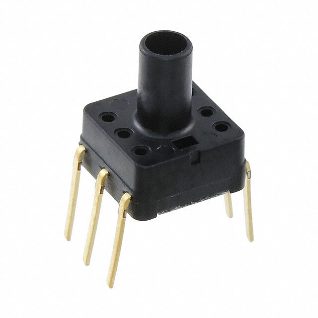
| 产品图片 |
|
| rohs | 符合RoHS无铅 / 符合限制有害物质指令(RoHS)规范要求 |
| 产品系列 | 板机接口压力传感器,STMicroelectronics LPS331APTR- |
| 数据手册 | |
| 产品型号 | LPS331APTR |
| 产品培训模块 | http://www.digikey.cn/PTM/IndividualPTM.page?site=cn&lang=zhs&ptm=30015http://www.digikey.cn/PTM/IndividualPTM.page?site=cn&lang=zhs&ptm=30339http://www.digikey.cn/PTM/IndividualPTM.page?site=cn&lang=zhs&ptm=30444 |
| 产品种类 | 板机接口压力传感器 |
| 其它名称 | 497-12927-6 |
| 其它有关文件 | http://www.st.com/web/catalog/sense_power/FM89/SC1316/PF251601?referrer=70071840 |
| 出厂设置 | - |
| 压力类型 | 绝对 |
| 商标 | STMicroelectronics |
| 安装风格 | SMD/SMT |
| 封装 | Reel |
| 封装/外壳 | 16-VFLGA |
| 封装/箱体 | HCLGA-16 |
| 工作压力 | 260 ~ 1260 mbar |
| 工作温度 | -40°C ~ 85°C |
| 工作电源电压 | 1.71 V to 3.6 V |
| 工厂包装数量 | 4000 |
| 最大工作温度 | + 85 C |
| 最小工作温度 | - 40 C |
| 标准包装 | 1 |
| 特色产品 | http://www.digikey.cn/product-highlights/cn/zh/stmicroelectronics-lsp331ap-pressure-sensor/3392 |
| 电压-电源 | 1.71 V ~ 3.6 V |
| 电源电压-最大 | 3.6 V |
| 电源电压-最小 | 1.71 V |
| 电源电流 | 0.5 uA |
| 端口尺寸 | 母型,0.016"(0.4mm)孔 |
| 端子类型 | 表面贴装型 |
| 精度 | ±2mbar |
| 系列 | LPS331AP |
| 输出 | 数字 |


- 商务部:美国ITC正式对集成电路等产品启动337调查
- 曝三星4nm工艺存在良率问题 高通将骁龙8 Gen1或转产台积电
- 太阳诱电将投资9.5亿元在常州建新厂生产MLCC 预计2023年完工
- 英特尔发布欧洲新工厂建设计划 深化IDM 2.0 战略
- 台积电先进制程称霸业界 有大客户加持明年业绩稳了
- 达到5530亿美元!SIA预计今年全球半导体销售额将创下新高
- 英特尔拟将自动驾驶子公司Mobileye上市 估值或超500亿美元
- 三星加码芯片和SET,合并消费电子和移动部门,撤换高东真等 CEO
- 三星电子宣布重大人事变动 还合并消费电子和移动部门
- 海关总署:前11个月进口集成电路产品价值2.52万亿元 增长14.8%

PDF Datasheet 数据手册内容提取
LPS331AP MEMS pressure sensor: 260-1260 mbar absolute digital output barometer − Datasheet production data Features ■ 260 to 1260 mbar absolute pressure range ■ High-resolution mode: 0.020 mbar RMS ■ Low power consumption: – Low resolution mode: 5.5 µA – High resolution mode: 30 µA ■ High overpressure capability: 20x full scale HCLGA-16L ■ Embedded temperature compensation (3 x 3 x1mm) ■ Embedded 24-bit ADC The sensing element consists of a suspended ■ Selectable ODR from 1 Hz to 25 Hz membrane realized inside a single mono-silicon ■ SPI and I2C interfaces substrate. It is capable to detecting pressure and ■ Supply voltage: 1.71 to 3.6 V is manufactured using a dedicated process developed by ST, called VENSENS. ■ High shock survivability: 10,000 g ■ Small and thin package The VENSENS process allows to build a mono- silicon membrane above an air cavity with ■ ECOPACK® lead-free compliant controlled gap and defined pressure. The membrane is very small compared to the Applications traditionally built silicon micromachined membranes. Membrane breakage is prevented by ■ Indoor and outdoor navigation an intrinsic mechanical stopper. ■ Enhanced GPS for dead-reckoning The IC interface is manufactured using a standard ■ Altimeter and barometer for portable devices CMOS process that allows a high level of ■ Weather station equipment integration to design a dedicated circuit which is trimmed to better match the sensing element ■ Sport watches characteristics. Description The LPS331AP is available in a small holed cap land grid array (HCLGA) package and it is The LPS331AP is an ultra compact absolute guaranteed to operate over a temperature range piezoresistive pressure sensor. It includes a extending from -40 °C to +85 °C. The package is monolithic sensing element and an IC interface holed to allow external pressure to reach the able to take the information from the sensing sensing element. element and to provide a digital signal to the external world. Table 1. Device summary Order codes Temperature range [°C] Package Packing LPS331APY Tray -40 to +85 HCLGA-16L LPS331APTR Tape and reel March 2012 Doc ID 022112 Rev 7 1/36 This is information on a product in full production. www.st.com 36
Contents LPS331AP Contents 1 Block diagram and pin description . . . . . . . . . . . . . . . . . . . . . . . . . . . . . 3 1.1 LPS331AP block diagram . . . . . . . . . . . . . . . . . . . . . . . . . . . . . . . . . . . . . . 3 1.2 Pin description . . . . . . . . . . . . . . . . . . . . . . . . . . . . . . . . . . . . . . . . . . . . . . 3 2 Mechanical and electrical specifications . . . . . . . . . . . . . . . . . . . . . . . . 5 2.1 Mechanical characteristics . . . . . . . . . . . . . . . . . . . . . . . . . . . . . . . . . . . . . 5 2.2 Electrical characteristics . . . . . . . . . . . . . . . . . . . . . . . . . . . . . . . . . . . . . . . 6 2.3 Absolute maximum ratings . . . . . . . . . . . . . . . . . . . . . . . . . . . . . . . . . . . . . 7 3 Functionality . . . . . . . . . . . . . . . . . . . . . . . . . . . . . . . . . . . . . . . . . . . . . . . 8 3.1 Sensing element . . . . . . . . . . . . . . . . . . . . . . . . . . . . . . . . . . . . . . . . . . . . . 8 3.2 IC interface . . . . . . . . . . . . . . . . . . . . . . . . . . . . . . . . . . . . . . . . . . . . . . . . . 8 3.3 Factory calibration . . . . . . . . . . . . . . . . . . . . . . . . . . . . . . . . . . . . . . . . . . . 8 4 Application hints . . . . . . . . . . . . . . . . . . . . . . . . . . . . . . . . . . . . . . . . . . . . 9 4.1 Soldering information . . . . . . . . . . . . . . . . . . . . . . . . . . . . . . . . . . . . . . . . . 9 5 Digital interfaces . . . . . . . . . . . . . . . . . . . . . . . . . . . . . . . . . . . . . . . . . . . 10 5.1 I2C serial interface . . . . . . . . . . . . . . . . . . . . . . . . . . . . . . . . . . . . . . . . . . 10 5.2 I2C serial interface . . . . . . . . . . . . . . . . . . . . . . . . . . . . . . . . . . . . . . . . . . 10 5.2.1 I2C operation . . . . . . . . . . . . . . . . . . . . . . . . . . . . . . . . . . . . . . . . . . . . . 11 5.3 SPI bus interface . . . . . . . . . . . . . . . . . . . . . . . . . . . . . . . . . . . . . . . . . . . 12 5.3.1 SPI read . . . . . . . . . . . . . . . . . . . . . . . . . . . . . . . . . . . . . . . . . . . . . . . . . 13 5.3.2 SPI write . . . . . . . . . . . . . . . . . . . . . . . . . . . . . . . . . . . . . . . . . . . . . . . . 14 5.3.3 SPI read in 3-wires mode . . . . . . . . . . . . . . . . . . . . . . . . . . . . . . . . . . . 15 6 Register mapping . . . . . . . . . . . . . . . . . . . . . . . . . . . . . . . . . . . . . . . . . . 16 7 Register description . . . . . . . . . . . . . . . . . . . . . . . . . . . . . . . . . . . . . . . . 17 8 Package mechanical section . . . . . . . . . . . . . . . . . . . . . . . . . . . . . . . . . 32 9 Revision history . . . . . . . . . . . . . . . . . . . . . . . . . . . . . . . . . . . . . . . . . . . 35 2/36 Doc ID 022112 Rev 7
LPS331AP Block diagram and pin description 1 Block diagram and pin description 1.1 LPS331AP block diagram Figure 1. LPS331AP block diagram p e CS d ur Rs VupRsVout MUX Low noise analog front en ADC+ digital filter SP for temperatcompensation IS2PCI SSSCDALA0///SSSPDDOCO/SDI Rs Rs D Vdown Temperature Sensing sensor element Voltage and Clock and timing current bias Sensor bias AM08736V1 1.2 Pin description Figure 2. Pin connection Pin 1 indicator 13 1 9 5 Bottom view AM08737V1 Doc ID 022112 Rev 7 3/36
Block diagram and pin description LPS331AP T able 2. Pin description Pin# Name Function 1 Vdd_IO Power supply for I/O pins 2 NC Not connected 3 NC Not connected SCL I2C serial clock (SCL) 4 SPC SPI serial port clock (SPC) 5 GND 0 V supply SDA I2C serial data (SDA) 6 SDI SPI serial data input (SDI) SDO 3-wire interface serial data output (SDO) SDO SPI serial data output (SDO) 7 SA0 I2C less significant bit of the device address (SA0) SPI enable 8 CS I2C/SPI mode selection (1: I2C mode; 0: SPI enabled) 9 INT2 Interrupt 2 (or data ready) 10 Reserved Connect to GND 11 INT1 Interrupt 1 (or data ready) 12 GND 0 V supply 13 GND 0 V supply 14 VDD Power supply 15 VCCA Analog power supply 16 GND 0 V supply 4/36 Doc ID 022112 Rev 7
LPS331AP Mechanical and electrical specifications 2 Mechanical and electrical specifications Conditions at V = 2.5 V, T = 25 °C, unless otherwise noted. DD 2.1 Mechanical characteristics T a. ble 3. Mechanical characteristics Symbol Parameter Test condition Min. Typ.(1) Max. Unit Top Operating temperature range -40 – 85 °C Full accuracy temperature Tfull 0 – 80 °C range Pop Operating pressure range 260 – 1260 mbar Pbits Pressure output data – 24 – bits LSB/ Pres Pressure sensitivity – 4096 – mbar Relative accuracy over P=800 to 1100 mbar Paccrel – ± 0.1 ± 0.2 mbar pressure(2) T= 25°C Absolute accuracy pressure P=800 to 1100 mbar PaccT - 3.2 ±2 2.6 mbar over temperature(3) T = 0 ∼ +80 °C mbar Pnoise Pressure noise See Table 17. RMS Tbits Temperature output data – 16 – bits Tres Temperature sensitivity – 480 – LSB/°C Tacc Absolute accuracy temperature T= 0~+80 °C – ±2 – °C 1. Typical specifications are not guaranteed. 2. Characterization data. Parameter not tested at final test 3. Embedded pwl compensation. Doc ID 022112 Rev 7 5/36
Mechanical and electrical specifications LPS331AP 2.2 Electrical characteristics T able 4. Electrical characteristics Symbol Parameter Test condition Min. Typ.(1) Max. Unit Vdd Supply voltage 1.71 – 3.6 V Vdd_IO IO supply voltage 1.71 – 3.6 V Supply current @ ODRp 1 Hz and Idd see Table5 µA ODRt = 1Hz Supply current in power-down mode IddPdn – 0.5 – µA T = 25 °C 1. Typical specifications are not guaranteed. T able 5. Supply current at ODRp 1 Hz, ODRt 1 Hz Symbol RES_CONF (hex) Min. Typ. Max. Unit 73 – 5.5 – 75 – 6.6 – Idd 77 – 11.5 – µA 78 – 17.5 – 7A – 30.0 – 6/36 Doc ID 022112 Rev 7
LPS331AP Mechanical and electrical specifications 2.3 Absolute maximum ratings Stress above those listed as “Absolute maximum ratings” may cause permanent damage to the device. This is a stress rating only and functional operation of the device under these conditions is not implied. Exposure to maximum rating conditions for extended periods may affect device reliability. T able 6. Absolute maximum ratings Symbol Ratings Maximum value Unit Vdd Supply voltage -0.3 to 4.8 V Vdd_IO I/O pins supply voltage -0.3 to 4.8 V Vin Input voltage on any control pin -0.3 to Vdd_IO +0.3 V P Overpressure 20 bar T Storage temperature range -40 to +125 °C STG ESD Electrostatic discharge protection 2 (HBM) kV Note: Supply voltage on any pin should never exceed 4.8V. This is a mechanical shock sensitive device, improper handling can cause permanent damage to the part. This is an ESD sensitive device, improper handling can cause permanent damage to the part. Doc ID 022112 Rev 7 7/36
Functionality LPS331AP 3 Functionality The LPS331AP is a high resolution, digital output pressure sensor packaged in an HCLGA holed package. The complete device includes a sensing element based on a piezoresistive Wheatstone bridge approach, and an IC interface able to take the information from the sensing element to the external world, as a digital signal. 3.1 Sensing element An ST proprietary process is used to obtain a mono-silicon µ-sized membrane for MEMS pressure sensors, without requiring substrate to substrate bonding. When pressure is applied, the membrane deflection induces an imbalance in the Wheatstone bridge piezoresistances, whose output signal is converted by the IC interface. Intrinsic mechanical stoppers prevent breakage in case of pressure overstress, ensuring measurement repeatability. The pressure inside the buried cavity under the membrane is constant and controlled by process parameters. 3.2 IC interface The complete measurement chain consists of a low-noise capacitive amplifier, which converts the resistive unbalance of the MEMS sensor into an analog voltage signal, and of an analog-to-digital converter, which translates the produced signal into a digital bitstream. The converter is coupled with a dedicated reconstruction filter which removes the high frequency components of the quantization noise and provides low rate and high resolution digital words. The pressure data can be accessed through an I2C/SPI interface making the device particularly suitable for direct interfacing with a microcontroller. 3.3 Factory calibration The IC interface is factory calibrated at three temperatures and two pressures for sensitivity and accuracy. The trimming values are stored inside the device by a non-volatile structure. Whenever the device is turned on, the trimming parameters are downloaded into the registers to be employed during normal operation. This allows the user to employ the device without requiring any further calibration. 8/36 Doc ID 022112 Rev 7
LPS331AP Application hints 4 Application hints Figure 3. LPS331AP electrical connection Vdd 16 14 10¬µ Vdd_IO 1 13 TOP VIEW Res 100nF 55 99 6 8 Res O D SCL/SPC SDA/SDI/S SDO/SA0 CS GND Digital signal from/to signal controller. Signal levels are defined through proper selection of Vdd_ The device core is supplied through the Vdd line. Power supply decoupling capacitors (100 nF ceramic, 10 µF aluminum) should be placed as near as possible to the supply pad of the device (common design practice). The functionality of the device and the measured data outputs are selectable and accessible through the I2C/SPI interface. When using the I2C, CS must be tied high (i.e. connected to Vdd_IO). 4.1 Soldering information The HCLGA package is compliant with the ECOPACK® standard and it is qualified for soldering heat resistance according to JEDEC J-STD-020. Doc ID 022112 Rev 7 9/36
Digital interfaces LPS331AP 5 Digital interfaces 2 5.1 I C serial interface The registers embedded in the LPS331AP may be accessed through both the I2C and SPI serial interfaces. The latter may be SW configured to operate either in 3-wire or 4-wire interface mode. The serial interfaces are mapped onto the same pads. To select/exploit the I2C interface, CS line must be tied high (i.e. connected to Vdd_IO). T able 7. Serial interface pin description Pin name Pin description SPI enable CS I2C/SPI mode selection (1: I2C mode; 0: SPI enabled) SCL/ I2C serial clock (SCL) SPC SPI serial port clock (SPC) SDA/ I2C serial data (SDA) SDI/ SPI serial data input (SDI) SDO 3-wire interface serial data output (SDO) SA0/ I2C less significant bit of the device address (SA0) SDO SPI serial data output (SDO) 2 5.2 I C serial interface The LPS331AP I2C is a bus slave. The I2C is employed to write data into registers whose content can also be read back. The relevant I2C terminology is given in Table 8. T able 8. Serial interface pin description Term Description Transmitter The device which sends data to the bus Receiver The device which receives data from the bus The device which initiates a transfer, generates clock signals and terminates a Master transfer Slave The device addressed by the master There are two signals associated with the I2C bus: the serial clock line (SCL) and the serial data line (SDA). The latter is a bi-directional line used for sending and receiving the data to/from the interface. Both lines have to be connected to Vdd_IO through pull-up resistors. The I2C interface is compliant with fast mode (400 kHz) I2C standards as well as with the normal mode. 10/36 Doc ID 022112 Rev 7
LPS331AP Digital interfaces 5.2.1 I2C operation The transaction on the bus is started through a START (ST) signal. A start condition is defined as a HIGH to LOW transition on the data line while the SCL line is held HIGH. After this has been transmitted by the master, the bus is considered busy. The next byte of data transmitted after the start condition contains the address of the slave in the first 7 bits and the eighth bit tells whether the master is receiving data from the slave or transmitting data to the slave. When an address is sent, each device in the system compares the first seven bits after a start condition with its address. If they match, the device considers itself addressed by the master. The slave address (SAD) associated to the LPS331AP is 101110xb. The SDO/SA0 pad can be used to modify the less significant bit of the device address. If the SA0 pad is connected to voltage supply, LSb is ‘1’ (address 1011101b), otherwise if the SA0 pad is connected to ground, the LSb value is ‘0’ (address 1011100b). This solution permits to connect and address two different LPS331APs to the same I2C lines. Data transfer with acknowledge is mandatory. The transmitter must release the SDA line during the acknowledge pulse. The receiver must then pull the data line LOW so that it remains stable low during the HIGH period of the acknowledge clock pulse. A receiver which has been addressed is obliged to generate an acknowledge after each byte of data received. The I2C embedded in the LPS331AP behaves like a slave device and the following protocol must be adhered to. After the start condition (ST) a slave address is sent, once a slave acknowledge (SAK) has been returned, a 8-bit sub-address (SUB) will be transmitted: the 7 LSB represents the actual register address while the MSB enables address auto increment. If the MSb of the SUB field is ‘1’, the SUB (register address) will be automatically increased to allow multiple data read/write. The slave address is completed with a Read/Write bit. If the bit was ‘1’ (Read), a repeated START (SR) condition must be issued after the two sub-address bytes; if the bit is ‘0’ (Write) the master will transmit to the slave with direction unchanged. Table9 explains how the SAD+read/write bit pattern is composed, listing all the possible configurations. Table 9. SAD+Read/Write patterns Command SAD[6:1] SAD[0] = SA0 R/W SAD+R/W Read 101110 0 1 10111001 (B9h) Write 101110 0 0 10111000 (B8h) Read 101110 1 1 10111011 (BBh) Write 101110 1 0 10111010 (BAh) Table 10. Transfer when master is writing one byte to slave Master ST SAD + W SUB DATA SP Slave SAK SAK SAK Table 11. Transfer when master is writing multiple bytes to slave Master ST SAD + W SUB DATA DATA SP Slave SAK SAK SAK SAK Doc ID 022112 Rev 7 11/36
Digital interfaces LPS331AP Table 12. Transfer when master is receiving (reading) one byte of data from slave Master ST SAD + W SUB SR SAD + R NMAK SP Slave SAK SAK SAK DATA Table 13. Transfer when master is receiving (reading) multiple bytes of data from slave Master ST SAD+W SUB SR SAD+R MAK MAK NMAK SP Slave SAK SAK SAK DATA DATA DATA Data are transmitted in byte format (DATA). Each data transfer contains 8 bits. The number of bytes transferred per transfer is unlimited. Data is transferred with the most significant bit (MSb) first. If a receiver can’t receive another complete byte of data until it has performed some other functions, it can hold the clock line, SCL LOW to force the transmitter into a wait state. Data transfer only continues when the receiver is ready for another byte and releases the data line. If a slave receiver does not acknowledge the slave address (i.e. it is not able to receive because it is performing some real time function) the data line must be kept HIGH by the slave. The master can then abort the transfer. A LOW to HIGH transition on the SDA line while the SCL line is HIGH is defined as a STOP condition. Each data transfer must be terminated by the generation of a STOP (SP) condition. In order to read multiple bytes incrementing the register address, it is necessary to assert the most significant bit of the sub-address field. In other words, SUB(7) must be equal to 1 while SUB(6-0) represents the address of the first register to be read. In the presented communication format MAK is Master acknowledge and NMAK is no master acknowledge. 5.3 SPI bus interface The LPS331AP SPI is a bus slave. The SPI allows to write and read the registers of the device. The serial interface interacts with the outside world with 4 wires: CS, SPC, SDI and SDO. Figure 4. Read and write protocol CS SPC SDI RW DI7 DI6 DI5 DI4 DI3 DI2 DI1 DI0 MS AD5 AD4AD3 AD2 AD1 AD0 SDO DO7DO6DO5DO4DO3DO2DO1DO0 CS is the serial port enable and it is controlled by the SPI master. It goes low at the start of the transmission and returns to high at the end. SPC is the serial port clock and it is controlled by the SPI master. It is stopped high when CS is high (no transmission). SDI and 12/36 Doc ID 022112 Rev 7
LPS331AP Digital interfaces SDO are respectively the serial port data input and output. Those lines are driven at the falling edge of SPC and should be captured at the rising edge of SPC. Both the read register and write register commands are completed in 16 clock pulses or in multiples of 8 in the case of multiple bytes read/write. Bit duration is the time between two falling edges of SPC. The first bit (bit 0) starts at the first falling edge of SPC after the falling edge of CS while the last bit (bit 15, bit 23, ...) starts at the last falling edge of SPC just before the rising edge of CS. bit 0: RW bit. When 0, the data DI(7:0) is written into the device. When 1, the data DO(7:0) from the device is read. In the latter case, the chip will drive SDO at the start of bit 8. bit 1: MS bit. When 0, the address will remain unchanged in multiple read/write commands. When 1, the address will be auto incremented in multiple read/write commands. bit 2-7: address AD(5:0). This is the address field of the indexed register. bit 8-15: data DI(7:0) (write mode). This is the data that is written into the device (MSb first). bit 8-15: data DO(7:0) (read mode). This is the data that is read from the device (MSb first). In multiple read/write commands further blocks of 8 clock periods are added. When the MS bit is 0 the address used to read/write data remains the same for every block. When MS bit is 1 the address used to read/write data is increased at every block. The function and the behavior of SDI and SDO remain unchanged. 5.3.1 SPI read Figure 5. SPI read protocol CS SPC SDI RW MSAD5AD4AD3AD2AD1AD0 SDO DO7DO6DO5DO4DO3DO2DO1DO0 The SPI Read command is performed with 16 clock pulses. The multiple byte read command is performed adding blocks of 8 clock pulses at the previous one. bit 0: READ bit. The value is 1. bit 1: MS bit. When 0 do not increment address, when 1 increment address in multiple reading. bit 2-7: address AD(5:0). This is the address field of the indexed register. bit 8-15: data DO(7:0) (read mode). This is the data that is read from the device (MSb first). bit 16-... : data DO(...-8). Further data in multiple byte readings. Doc ID 022112 Rev 7 13/36
Digital interfaces LPS331AP Figure 6. Multiple bytes SPI read protocol (2 bytes example) CS SPC SDI RW MS AD5AD4AD3AD2AD1AD0 SDO DO7DO6DO5DO4DO3DO2DO1DO0DO15D O14D O13D O12D O11D O10D O9DO8 5.3.2 SPI write Figure 7. SPI write protocol CS SPC SDI RW DI7 DI6 DI5 DI4 DI3 DI2 DI1 DI0 MS AD5 AD4AD3 AD2 AD1 AD0 The SPI Write command is performed with 16 clock pulses. The multiple byte write command is performed adding blocks of 8 clock pulses at the previous one. bit 0: WRITE bit. The value is 0. bit 1: MS bit. When 0 do not increment the address, when 1 increment the address in multiple writings. bit 2 -7: address AD(5:0). This is the address field of the indexed register. bit 8-15: data DI(7:0) (write mode). This is the data that is written in the device (MSb first). bit 16-... : data DI(...-8). Further data in multiple byte writings. Figure 8. Multiple bytes SPI write protocol (2 bytes example) CS SPC SDI DI7 DI6 DI5 DI4 DI3 DI2 DI1 DI0 DI15 DI14 DI13 DI12 DI11 DI10 DI9 DI8 RW MSAD5AD4AD3AD2AD1AD0 14/36 Doc ID 022112 Rev 7
LPS331AP Digital interfaces 5.3.3 SPI read in 3-wires mode A 3-wires mode is entered by setting to ‘1’ bit SIM (SPI serial interface mode selection) in CTRL_REG4. Figure 9. SPI read protocol in 3-wires mode CS SPC SDI/O RW DO7 DO6 DO5 DO4 DO3 DO2 DO1 DO0 MS AD5 AD4 AD3 AD2 AD1 AD0 The SPI read command is performed with 16 clock pulses: bit 0: READ bit. The value is 1. bit 1: MS bit. When 0, do not increment the address, when 1, increment the address in multiple readings. bit 2-7: address AD(5:0). This is the address field of the indexed register. bit 8-15: data DO(7:0) (read mode). This is the data that is read from the device (MSb first). Multiple read command is also available in 3-wires mode. Doc ID 022112 Rev 7 15/36
Register mapping LPS331AP 6 Register mapping Table14 provides a list of the 8-bit registers embedded in the device and the related addresses. T a. ble 14. Registers address map Register Address Function and Name Type Default comment Hex Binary 00-07 Reserved (Do not modify) Reserved 0D - 0E REF_P_XL R/W 08 0001000 00000000 REF_P_L R/W 09 0001001 00000000 REF_P_H R/W 0A 0001010 00000000 WHO_AM_I R 0F 0001111 10111011 Dummy register RES_CONF R/W 10 0010000 011111010 Reserved (Do not modify) 11-1F Reserved CTRL_REG1 R/W 20 010 0000 00000000 CTRL_REG2 R/W 21 010 0001 00000000 CTRL_REG3 R/W 22 010 0010 00000000 INT_CFG_REG R/W 23 0100011 00000000 INT_SOURCE_REG R 24 0100100 00000000 THS_P_LOW_REG R/W 25 0100101 0000000 THS_P_HIGH_REG R/W 26 0100110 0000000 STATUS_REG R 27 010 0111 00000000 PRESS_POUT_XL_REH R 28 010 1000 output PRESS_OUT_L R 29 010 1001 output PRESS_OUT_H R 2A 010 1010 output TEMP_OUT_L R 2B 010 1011 output TEMP_OUT_H R 2C 010 1100 output Reserved (Do not modify) 2D-2F Reserved AMP_CTRL R/W 30 011 0000 Partially reserved Registers marked as Reserved must not be changed. The writing to those registers may cause permanent damages to the device. The content of the registers that are loaded at boot should not be changed. They contain the factory calibration values. Their content is automatically restored when the device is powered-up. 16/36 Doc ID 022112 Rev 7
LPS331AP Register description 7 Register description The device contains a set of registers which are used to control its behavior and to retrieve pressure and temperature data. The register address, made up of 7 bits, is used to identify them and to read/write the data through the serial interface. REF_P_XL Reference pressure (LSB data) 7 6 5 4 3 2 1 0 REFL7 REFL6 REFL5 REFL4 REFL3 REFL2 REFL1 REFL0 Address: 08h Type: R/W Reset: 00h Description: This reference pressure register contains the lower part of the reference pressure that is sum to the sensor output pressure. The full value is REF_P_XL & REF_P_H & REF_P_L and is represented as 2’s complement. [7:0] REFL7 - REFL0: Reference pressure LSB data. Default value: 00h REF_P_L Reference pressure (middle part) 16 15 14 13 12 11 10 9 REFL15 REFL14 REFL13 REFL12 REFL11 REFL10 REFL9 REFL8 Address: 09h Type: R/W Reset: 00h Description: This register contains the middle part of the reference pressure that is sum to the sensor output pressure. The full value is REF_P_XL & REF_P_H & REF_P_L and is represented as 2’s complement. [16:9] REFL15 - REFL8: Default value: 00h Doc ID 022112 Rev 7 17/36
Register description LPS331AP REF_P_H Reference pressure (MSB data) 24 23 22 21 20 19 18 17 REFL23 REFL22 REFL21 REFL20 REFL19 REFL18 REFL17 REFL16 Address: 0Ah Type: R/W Reset: 00h Description: This register contains the higher part of the reference pressure that is sum to the sensor output pressure. The full value is REF_P_XL & REF_P_H & REF_P_L and is represented as 2’s complement. [24:17] REFL23 - REFL16: Reference pressure MSB data. Default value: 00h. RES_CONF(10h) Pressure resolution mode 7 6 5 4 3 2 1 0 RFU AVGT2 AVGT1 AVGT0 AVGP3 AVGP2 AVGP1 AVGP0 Address: 10h Type: R/W Reset: 7Ah Description: AVGP3-AVGP0 allow to select the pressure internal average. AVGT2-AVGT0 allow to select the temperature internal average. AVGP3-AVGP0 bits can be configured as described in Table15. AVGT2-AVGT0 bits can be configured as described in Table16. Table 15. Pressure resolution configuration AVGP3 AVGP2 AVGP1 AVGP0 Nr. internal average 0 0 0 0 1 0 0 0 1 2 0 0 1 0 4 0 0 1 1 8 0 1 0 0 16 0 1 0 1 32 0 1 1 0 64 0 1 1 1 128 1 0 0 0 256 18/36 Doc ID 022112 Rev 7
LPS331AP Register description Table 15. Pressure resolution configuration AVGP3 AVGP2 AVGP1 AVGP0 Nr. internal average 1 0 0 1 384 1 0 1 0 512(1) 1. Register configuration 7Ah not allowed with ODR = 25Hz/25Hz (Register CTRL_REG1). For ORD 25Hz/25Hz the suggested configuration for RES_CONF is 6Ah. Table 16. Temperature resolution configuration AVGT2 AVGT1 AVGT1 Nr. internal average 0 0 0 1 0 0 1 2 0 1 0 4 0 1 1 8 1 0 0 16 1 0 1 32 1 1 0 64 1 1 1 128(1) 1. Register configuration 7Ah not allowed with ODR = 25Hz/25Hz (Register CTRL_REG1). For ORD 25Hz/25Hz the suggested configuration for RES_CONF is 6Ah. Table 17. Pressure resolution RES_CONF (hex) RMS noise(1) Unit 70 0.450 71 0.320 72 0.230 73 0.160 74 0.110 75 0.080 mbar 76 0.060 77 0.040 78 0.030 79 0.025 7A(2) 0.020 1. Rms noise is calculated as standard deviation of 10 data points. 2. This configuration is not allowed for ODR = 25Hz/25HZ (register CTRL_REG1). For ORD = 25Hz/25Hz the suggested configuration for RES_CONF is 6Ah. Doc ID 022112 Rev 7 19/36
Register description LPS331AP WHO_AM_I Device identification 7 6 5 4 3 2 1 0 1 0 1 1 1 0 1 1 Address: 0Fh Type: R Description: This read-only register contains the device identifier that, for LPS331AP, is set to BBh. CTRL_REG1 Control register 1 7 6 5 4 3 2 1 0 PD ODR2 ODR1 ODR0 DIFF_EN DBDU DELTA_EN SIM Address: 20h Type: R/W Description: Control register. [7] PD: power down control. Default value: 0 (0: power-down mode; 1: active mode) [6:4] ODR2, ODR1, ODR0: output data rate selection. Default value: 00 (see Table18) [3] DIFF_EN: Interrupt circuit enable. Default value: 0 (0: interrupt generation disabled; 1: interrupt circuit enabled) [2] BDU: block data update. Default value: 0 (0: continuous update; 1: output registers not updated until MSB and LSB reading) [1] DELTA_EN: delta pressure enable (1: delta pressure registers enabled. 0: disable) [0] SIM: SPI Serial Interface Mode selection. Default value: 0 (0: 4-wire interface; 1: 3-wire interface) PD bit allows to turn on the device. The device is in power-down mode when PD = ‘0’ (default value after boot). The device is active when PD is set to ‘1’. ODR2- ODR1 - ODR0 bits allow to change the output data rates of pressure and temperature samples. The default value is “000” which corresponds to “one shot configuration” for both pressure and temperature output. ODR2, ODR1 and ODR0 bits can be configured as described in Table18. Note: Before changing the ODR it is necessary to power down the device (CTRL_REG1[7]). 20/36 Doc ID 022112 Rev 7
LPS331AP Register description T able 18. Output data rate bit configurations Temperature output data ODR2 ODR1 ODR0 Pressure output data rate rate 0 0 0 One shot One shot 0 0 1 1Hz 1Hz 0 1 0 7Hz 1Hz 0 1 1 12.5Hz 1Hz 1 0 0 25Hz 1Hz 1 0 1 7Hz 7Hz 1 1 0 12.5Hz 12.5Hz 1 1 1 25Hz 25Hz DIFF_EN bit is used to enable the circuitry for the computing of differential pressure output. In default mode (DIF_EN=’0’) the circuitry is turned off. It is suggested to turn on the circuitry only after the configuration of REF_P_x and THS_P_x. BDU bit is used to inhibit the output registers update between the reading of upper and lower register parts. In default mode (BDU = ‘0’), the lower and upper register parts are updated continuously. If it is not sure to read faster than output data rate, it is recommended to set BDU bit to ‘1’. In this way, after the reading of the lower (upper) register part, the content of that output registers is not updated until the upper (lower) part is read too. This feature avoids reading LSB and MSB related to different samples. SIM bit selects the SPI serial interface mode. When SIM is ‘0’ (default value) the 4-wire interface mode is selected and data coming from the device are sent to pin #7 (SDO). In 3-wire interface mode, output data are sent to pin #6 (SDI/SDO). Doc ID 022112 Rev 7 21/36
Register description LPS331AP CTRL_REG2 Control register 2 7 6 5 4 3 2 1 0 BOOT RESERVED SWRESET AUTO_ZERO ONE_SHOT Address: 21h Type: R/W Description: Control register. [7] BOOT: Reboot memory content. Default value: 0 (0: normal mode; 1: reboot memory content) [6:3] RESERVED [2] Software reset. Default value: 0 (0: normal mode; 1: software reset) [1] Autozero enable. Default value: 0 (0: normal mode; 1: autozero enable) [0] One shot enable. Default value: 0 (0: waiting for start of conversion; 1: start for a new dataset) BOOT bit is used to refresh the content of the internal registers stored in the Flash memory block. At the device power-up the content of the Flash memory block is transferred to the internal registers related to trimming functions to permit a good behavior of the device itself. If for any reason, the content of the trimming registers is modified, it is sufficient to use this bit to restore the correct values. When BOOT bit is set to ‘1’ the content of the internal Flash is copied inside the corresponding internal registers and is used to calibrate the device. These values are factory trimmed and they are different for every device. They permit good behavior of the device and normally they should not be changed. At the end of the boot process the BOOT bit is set again to ‘0’. BOOT bit takes effect after one ODR clock cycle. SWRESET is the software reset bit. The device is reset to the power on configuration if the SWRESET bit is set to ‘1’ and BOOT is set to ‘1’. AUTO_ZERO, when set to ‘1’, the actual pressure output is copied in the REF_P_H & REF_P_L & REF_P_XL and kept as reference and the PRESS_OUT_H & PRESS_OUT_L & PRESS _OUT_XL is the difference between this reference and the pressure sensor value. ONE_SHOT bit is used to start a new conversion when ODR1-ODR0 bits in CTRL_REG1 are set to “000”. In this situation a single acquisition of temperature and pressure is started when ONE_SHOT bit is set to ‘1’. At the end of conversion the new data are available in the output registers, the STAUS_REG[0] and STAUS_REG[1] bits are set to ‘1’ and the ONE_SHOT bit comes back to ‘0’ by hardware. 22/36 Doc ID 022112 Rev 7
LPS331AP Register description CTRL_REG3 Interrupt control 7 6 5 4 3 2 1 0 INT_H_L PP_OD INT2_S3 INT2_S2 INT2_S1 INT1_S3 INT1_S2 INT1S1 Address: 22h Type: R/W Description: Control register. [7] INT_H_L: Interrupt active high, low. Default value: 0 (0: active high; 1: active low) [6] PP_OD: Push-pull/open drain selection on interrupt pads. Default value: 0 (0: push-pull; 1: open drain) [5:3] INT2_S3, INT2_S2, INT2_S1: data signal on INT2 pad control bits. Default value: 00 (see Table 19.) [2:0 INT1_S3, INT1_S2, INT1_S1: data signal on INT1 pad control bits. Default value: 00 (see Table 19.) Table 19. Interrupt configurations INT1(2)_S3 INT1(2)_S2 INT1(2)S1 INT1(2) pin 0 0 0 GND 0 0 1 Pressure high (P_high) 0 1 0 Pressure low (P_low) 0 1 1 P_low OR P_high 1 0 0 Data ready 1 0 1 Reserved 1 1 0 Reserved 1 1 1 Tri-state The device features two fully-programmable interrupt sources (INT1 and INT2) which may be configured to trigger different pressure events. Figure10 shows the block diagram of the interrupt generation block and output pressure data. The device may also be configured to generate, through interrupt pins, a Data Ready signal (Drdy) which indicates when a new measured pressure data is available, thus simplifying data synchronization in digital systems. Doc ID 022112 Rev 7 23/36
Register description LPS331AP Figure 10. Interrupt generation block and output pressure data. + Sensor output pressure PRESS_OUT_H & PRESS_OUT_L & PRESS_OUT_XL - + Low Press Interrupt Reference Pressure - PL REF_P_H & REF_P_L & REF_P_XL + High Press Interrupt Pressure Threshold -1 - PH THS_P_H & THS_P_L High press int Positive Press Threshold Reference Press Press Threshold Negative Low press int AM08738V1 INTERRUPT_CFG Interrupt configuration 7 6 5 4 3 2 1 0 RESERVED LIR PL_E PH_E Address: 23h Type: R/W Reset: 00h Description: Interrupt configuration. [7:3] RESERVED [2] LIR: Latch Interrupt request into INT_SOURCE register. Default value: 0. (0: interrupt request not latched; 1: interrupt request latched) [1] PL_E: Enable interrupt generation on differential pressure low event. Default value: 0. (0: disable interrupt request; 1: enable interrupt request on measured differential pressure value lower than preset threshold) [0] PH_E: Enable interrupt generation on differential pressure high event. Default value: 0 (0: disable interrupt request; 1:enable interrupt request on measured differential pressure value higher than preset threshold) 24/36 Doc ID 022112 Rev 7
LPS331AP Register description INT_SOURCE Interrupt source 7 6 5 4 3 2 1 0 0 0 0 0 0 IA PL PH Address: 24h Type: R Reset: 00h Description: INT_SOURCE register is cleared by reading INT_ACK register. [7:3] 0 [2] IA: Interrupt Active. (0: no interrupt has been generated; 1: one or more interrupt events have been generated). [1] PL: Differential pressure Low. (0: no interrupt has been generated; 1: Low differential pressure event has occurred). [0] PH: Differential pressure High. (0: no interrupt has been generated; 1: High differential pressure event has occurred). THS_P_L Threshold pressure (LSB) 7 6 5 4 3 2 1 0 THS7 THS6 THS5 THS4 THS3 THS2 THS1 THS0 Address: 25h Type: R/W Reset: 00h Description: This register contains the low part of threshold value for pressure interrupt generation. The complete threshold value is given by THS_P_H & THS_P_L and is expressed as unsigned number. [7:0] THS7 - THS0: Threshold pressure LSB. Default value: 00h. Doc ID 022112 Rev 7 25/36
Register description LPS331AP THS_P_H Threshold pressure (MSB) 15 14 13 12 11 10 9 8 THS15 THS14 THS13 THS12 THS11 THS10 THS9 THS8 Address: 26h Type: R/W Reset: 00h Description: This register contains the high part of the threshold value for pressure interrupt generation. The complete threshold value is given by THS_P_H & THS_P_L and is expressed as unsigned number. P_ths(mbar)=(THS_P_H & THS_P_L)[dec]/16. [15:8] THS7 - THS0: Threshold pressure MSB. Default value: 00h. STATUS_REG Status register 7 6 5 4 3 2 1 0 0 0 P_OR T_OR 0 0 P_DA T_DA Address: 27h Type: R Reset: 00h Description: The content of this register is updated every ODR cycle, regardless of BDU value in CTRL_REG1. P_DA is set to 1 whenever a new pressure sample is available. P_DA is cleared anytime PRESS_OUT_H (29h) register is read. T_DA is set to 1 whenever a new temperature sample is available. T_DA is cleared anytime TEMP_OUT_H (2Bh) register is read. P_OR bit is set to '1' whenever new pressure data is available and P_DA was set in the previous ODR cycle and not cleared. P_OR is cleared anytime PRESS_OUT_H (29h) register is read. T_OR is set to ‘1’ whenever new temperature data is available and T_DA was set in the previous ODR cycle and not cleared. T_OR is cleared anytime TEMP_OUT_H (2Bh) register is read. [7:6] 0 [5] P_OR: Pressure data overrun. Default value: 0 (0: no overrun has occurred; 1: new data for pressure has overwritten the previous one) [4] T_OR: Temperature data overrun. Default value: 0 (0: no overrun has occurred; 1: a new data for temperature has overwritten the previous one) 26/36 Doc ID 022112 Rev 7
LPS331AP Register description [3:2] 0 [1] P_DA: Pressure data available. Default value: 0 (0: new data for pressure is not yet available; 1: new data for pressure is available) [0] T_DA: Temperature data available. Default value: 0 (0: new data for temperature is not yet available; 1: new data for temperature is available) PRESS_OUT_XL Pressure data (LSB) 7 6 5 4 3 2 1 0 POUT7 POUT6 POUT5 POUT4 POUT3 POUT2 POUT1 POUT0 Address: 28h Type: R Reset: 00h Description: Pressure data. [7:0] POUT7 - POUT0: Pressure data LSB PRESS_OUT_L Pressure data 15 14 13 12 11 10 9 8 POUT15 POUT14 POUT13 POUT12 POUT11 POUT10 POUT9 POUT8 Address: 29h Type: R Reset: 80 Description: Pressure data. [15:8] POUT15 - POUT8: Pressure data Doc ID 022112 Rev 7 27/36
Register description LPS331AP PRESS_OUT_H (2Ah) Pressure data (MSB) 24 23 22 21 20 19 18 17 POUT23 POUT22 POUT21 POUT20 POUT19 POUT18 POUT17 POUT16 Address: 2Ah Type: R Reset: 2F Description: Pressure data are expressed as PRESS_OUT_H & PRESS_OUT_L & PRESS_OUT_XL in 2’s complement. Values exceeding the operating pressure Range (see Table 3) are clipped. Pressure output data: Pout(mbar)=(PRESS_OUT_H & PRESS_OUT_L & PRESS_OUT_XL)[dec]/4096 [24:17] POUT23 - POUT16: Pressure data MSB 28/36 Doc ID 022112 Rev 7
LPS331AP Register description TEMP_OUT_L (2Bh) Temperature data (LSB) 7 6 5 4 3 2 1 0 TOUT7 TOUT6 TOUT5 TOUT4 TOUT3 TOUT2 TOUT1 TOUT0 Address: 2Bh Type: R Reset: 00h [7:0] TOUT7 - TOUT0: temperature data LSBl TEMP_OUT_H (2Ch) Temperature data (MSB) 15 14 13 12 11 10 9 8 TOUT15 TOUT14 TOUT13 TOUT12 TOUT11 TOUT10 TOUT9 TOUT8 Address: 2Ch Type: R Reset: 00h [15:8] TOUT15 - TOUT8: temperature data MSB. Temperature data are expressed as TEMP_OUT_H & TEMP_OUT_L as 2’s complement numbers. Temperature output data: T(degC) = 42.5 + (Temp_OUTH & TEMP_OUT_L)[dec]/480 Doc ID 022112 Rev 7 29/36
Register description LPS331AP AMP_CTRL Analog front end control 7 6 5 4 3 2 1 0 RESERVED SELMAIN Address: 2Dh Type: R/W Reset: 00h [7:1] RESERVED [0] SELMAIN: Current of operational amplifier selector ‘1’ always high current ‘0’ high current during pressure acquisition and low current during temperature acquisition DELTA_PRESS_XL (3Ch) Pressure offset 7 6 5 4 3 2 1 0 DELTA7 DELTA6 DELTA5 DELTA4 DELTA3 DELTA2 DELTA1 DELTA0 Address: 3Ch Type: R/W Reset: 00h [7:0] DELTA0 - DELTA7: Delta pressure register for One Point calibration DELTA_PRESS_L (3Dh) Pressure offset 15 14 13 12 11 10 9 8 DELTA15 DELTA14 DELTA13 DELTA12 DELTA11 DELTA10 DELTA9 DELTA8 Address: 3Dh Type: R/W Reset: 00h [15:8] DELTA15-DELTA8: Delta pressure register for One Point calibration 30/36 Doc ID 022112 Rev 7
LPS331AP Register description DELTA_PRESS_L (3Eh) Pressure offset 24 23 22 21 20 19 18 17 DELTA23 DELTA22 DELTA21 DELTA20 DELTA19 DELTA18 DELTA17 DELTA16 Address: 3Eh Type: R/W Reset: 00h [23:16] DELTA23-DELTA16: Delta pressure register for One Point calibration DELTA_PRESS registers are used to store the one point calibration value to eliminate accuracy shift after soldering. DELTA_PRESS acts on the output pressure when CTRL_REG1[1] DELTA_EN is set to ‘1’. Doc ID 022112 Rev 7 31/36
Package mechanical section LPS331AP 8 Package mechanical section In order to meet environmental requirements, ST offers these devices in different grades of ECOPACK® packages, depending on their level of environmental compliance. ECOPACK® specifications, grade definitions and product status are available at: www.st.com. ECOPACK is an ST trademark. Figure 11. Package outline for HCLGA-16L (3 x 3 x 1 mm) 32/36 Doc ID 022112 Rev 7
LPS331AP Package mechanical section Table 20. HCLGA-16L (3 x 3 x 1 mm) mechanical data Millimeters Symbol Min Typ Max E1 2.850 3.000 3.150 E3 – 0 – D1 2.850 3.000 3.150 D3 – 0.700 – R1 – 0.400 – A1 – 1.000 – L1 – 1.000 – N1 – 0.500 – L2 – 2.000 – N2 – 1.000 – P1 – 0.875 – P2 – 1.275 – T1 – 0.350 – T2 – 0.250 – d – 0.150 – K – 0.050 – M – 0.100 – Figure 12. Tray information Doc ID 022112 Rev 7 33/36
Package mechanical section LPS331AP Figure 13. Tape information 34/36 Doc ID 022112 Rev 7
LPS331AP Revision history 9 Revision history Table 21. Document revision history Date Revision Changes 12-Aug-2011 1 Initial release. – Updated order code in Table1: Device summary 16-Aug-2011 2 – Minor formatting and text modifications throughout the document – Updated: features list, Table3, Table6, Section4 and Section7. 20-Oct-2011 3 – Added: Table17, Figure12 and Figure13. – Modified: minor text updates in the Features section, Table3, 15-Dec-2011 4 Table4, Table5, Section3.1: Sensing element and Figure11. Modified: – Temperature range in Table1 from “-20 to +105” to “-40 to +85”. – Temperature output data in register TEMP_OUT_H (2Ch) from “42.5” to “22.5”. 13-Jan-2012 5 – PaccT test condition data in Table3 from “P=260 to 1260 mbar” to “P=800 to 1100 mbar” – Device operating range in Description on page1 from “-20 °C to +105 °C” to “-40 °C to +85 °C” Document status promoted from preliminary data to datasheet. Modified: – Temperature output data in register TEMP_OUT_H (2Ch) from 27-Feb-2012 6 “22.5” to “42.5” – Added register address in register DELTA_PRESS_XL (3Ch) and modified register address in DELTA_PRESS_L from “3Dh” to “3Eh”. Modified the description for pin 14 inTable2 and the list of 29-Mar-2012 7 applications in the cover page. Doc ID 022112 Rev 7 35/36
LPS331AP Please Read Carefully: Information in this document is provided solely in connection with ST products. STMicroelectronics NV and its subsidiaries (“ST”) reserve the right to make changes, corrections, modifications or improvements, to this document, and the products and services described herein at any time, without notice. All ST products are sold pursuant to ST’s terms and conditions of sale. Purchasers are solely responsible for the choice, selection and use of the ST products and services described herein, and ST assumes no liability whatsoever relating to the choice, selection or use of the ST products and services described herein. No license, express or implied, by estoppel or otherwise, to any intellectual property rights is granted under this document. If any part of this document refers to any third party products or services it shall not be deemed a license grant by ST for the use of such third party products or services, or any intellectual property contained therein or considered as a warranty covering the use in any manner whatsoever of such third party products or services or any intellectual property contained therein. UNLESS OTHERWISE SET FORTH IN ST’S TERMS AND CONDITIONS OF SALE ST DISCLAIMS ANY EXPRESS OR IMPLIED WARRANTY WITH RESPECT TO THE USE AND/OR SALE OF ST PRODUCTS INCLUDING WITHOUT LIMITATION IMPLIED WARRANTIES OF MERCHANTABILITY, FITNESS FOR A PARTICULAR PURPOSE (AND THEIR EQUIVALENTS UNDER THE LAWS OF ANY JURISDICTION), OR INFRINGEMENT OF ANY PATENT, COPYRIGHT OR OTHER INTELLECTUAL PROPERTY RIGHT. UNLESS EXPRESSLY APPROVED IN WRITING BY TWO AUTHORIZED ST REPRESENTATIVES, ST PRODUCTS ARE NOT RECOMMENDED, AUTHORIZED OR WARRANTED FOR USE IN MILITARY, AIR CRAFT, SPACE, LIFE SAVING, OR LIFE SUSTAINING APPLICATIONS, NOR IN PRODUCTS OR SYSTEMS WHERE FAILURE OR MALFUNCTION MAY RESULT IN PERSONAL INJURY, DEATH, OR SEVERE PROPERTY OR ENVIRONMENTAL DAMAGE. ST PRODUCTS WHICH ARE NOT SPECIFIED AS "AUTOMOTIVE GRADE" MAY ONLY BE USED IN AUTOMOTIVE APPLICATIONS AT USER’S OWN RISK. Resale of ST products with provisions different from the statements and/or technical features set forth in this document shall immediately void any warranty granted by ST for the ST product or service described herein and shall not create or extend in any manner whatsoever, any liability of ST. ST and the ST logo are trademarks or registered trademarks of ST in various countries. Information in this document supersedes and replaces all information previously supplied. The ST logo is a registered trademark of STMicroelectronics. All other names are the property of their respective owners. © 2012 STMicroelectronics - All rights reserved STMicroelectronics group of companies Australia - Belgium - Brazil - Canada - China - Czech Republic - Finland - France - Germany - Hong Kong - India - Israel - Italy - Japan - Malaysia - Malta - Morocco - Philippines - Singapore - Spain - Sweden - Switzerland - United Kingdom - United States of America www.st.com 36/36 Doc ID 022112 Rev 7