ICGOO在线商城 > 集成电路(IC) > 嵌入式 - 微控制器 > LPC812M101JDH20FP
 Datasheet下载
- 型号: LPC812M101JDH20FP
- 制造商: NXP Semiconductors
- 库位|库存: xxxx|xxxx
- 要求:
| 数量阶梯 | 香港交货 | 国内含税 |
| +xxxx | $xxxx | ¥xxxx |
查看当月历史价格
查看今年历史价格
LPC812M101JDH20FP产品简介:
ICGOO电子元器件商城为您提供LPC812M101JDH20FP由NXP Semiconductors设计生产,在icgoo商城现货销售,并且可以通过原厂、代理商等渠道进行代购。 LPC812M101JDH20FP价格参考¥18.26-¥18.26。NXP SemiconductorsLPC812M101JDH20FP封装/规格:嵌入式 - 微控制器, ARM® Cortex®-M0+ 微控制器 IC LPC81xM 32-位 30MHz 16KB(16K x 8) 闪存 20-TSSOP。您可以下载LPC812M101JDH20FP参考资料、Datasheet数据手册功能说明书,资料中有LPC812M101JDH20FP 详细功能的应用电路图电压和使用方法及教程。
NXP USA Inc.生产的LPC812M101JDH20FP是一款基于ARM Cortex-M0+内核的低功耗微控制器,属于嵌入式微控制器系列。其应用场景广泛,适用于多种需要高性能、低功耗和小尺寸设计的领域。以下是该型号微控制器的主要应用场景:

1. 消费电子:可用于智能家居设备(如智能插座、灯光控制模块)、家用电器(如咖啡机、电风扇)等,提供高效的控制功能和低功耗特性。

2. 工业自动化:在传感器数据采集、电机控制、小型工业设备的监控与管理中发挥重要作用。其丰富的外设接口(如UART、SPI、I2C)便于连接各种传感器和执行器。

3. 物联网(IoT)设备:作为小型物联网节点的核心,支持低功耗运行,适合电池供电的无线传感网络设备或环境监测装置。

4. 便携式设备:由于其低功耗特性和较小的封装尺寸,非常适合应用于便携式医疗设备(如血糖仪、脉搏血氧仪)或个人健康追踪器。

5. 汽车电子:可用于简单的车载诊断系统、车内照明控制、车窗升降控制等对成本敏感但可靠性要求较高的场景。

6. 教育与开发:因其易于使用且开发资源丰富,常被用作教学工具或开发板的核心组件,帮助学生和工程师学习嵌入式系统设计。

LPC812M101JDH20FP具备20引脚的QFN封装,内置16KB闪存和4KB SRAM,集成多种模拟和数字外设,能够满足许多基础及中端应用需求,同时保持较低的成本和功耗。这些特点使其成为众多嵌入式项目中的理想选择。
| 参数 | 数值 |
| A/D位大小 | No ADC |
| 产品目录 | 集成电路 (IC)半导体 |
| 描述 | IC MCU ARM 16KB FLASH 20TSSOPARM微控制器 - MCU 32-bit ARM CortexM0+ Microcontroller |
| EEPROM容量 | - |
| 产品分类 | |
| I/O数 | 18 |
| 品牌 | NXP Semiconductors |
| 产品手册 | |
| 产品图片 |
|
| rohs | 符合RoHS无铅 / 符合限制有害物质指令(RoHS)规范要求 |
| 产品系列 | 嵌入式处理器和控制器,微控制器 - MCU,ARM微控制器 - MCU,NXP Semiconductors LPC812M101JDH20FPLPC81xM |
| 数据手册 | |
| 产品型号 | LPC812M101JDH20FP |
| PCN封装 | |
| RAM容量 | 4K x 8 |
| 产品培训模块 | http://www.digikey.cn/PTM/IndividualPTM.page?site=cn&lang=zhs&ptm=30449 |
| 产品种类 | ARM微控制器 - MCU |
| 供应商器件封装 | 20-TSSOP |
| 其它名称 | 568-10437-5 |
| 包装 | 管件 |
| 可编程输入/输出端数量 | 18 |
| 商标 | NXP Semiconductors |
| 商标名 | LPC |
| 处理器系列 | LPC81xM |
| 外设 | 欠压检测/复位,POR,PWM,WDT |
| 安装风格 | SMD/SMT |
| 定时器数量 | 3 Timer |
| 封装 | Tube |
| 封装/外壳 | 20-TSSOP(0.173",4.40mm 宽) |
| 封装/箱体 | TSSOP-20 |
| 工作温度 | -40°C ~ 105°C |
| 工作电源电压 | 1.8 V to 3.6 V |
| 工厂包装数量 | 750 |
| 振荡器类型 | 内部 |
| 接口类型 | I2C, SPI, USART |
| 数据RAM大小 | 4 kB |
| 数据Ram类型 | SRAM |
| 数据总线宽度 | 32 bit |
| 数据转换器 | - |
| 最大工作温度 | + 105 C |
| 最大时钟频率 | 30 MHz |
| 最小工作温度 | - 40 C |
| 标准包装 | 75 |
| 核心 | ARM Cortex M0 |
| 核心处理器 | ARM® Cortex™-M0+ |
| 核心尺寸 | 32-位 |
| 片上ADC | No |
| 电压-电源(Vcc/Vdd) | 1.8 V ~ 3.6 V |
| 程序存储器大小 | 16 kB |
| 程序存储器类型 | Flash |
| 程序存储容量 | 16KB(16K x 8) |
| 系列 | LPC800 |
| 输入/输出端数量 | 18 I/O |
| 连接性 | I²C, SPI, UART/USART |
| 速度 | 30MHz |


- 商务部:美国ITC正式对集成电路等产品启动337调查
- 曝三星4nm工艺存在良率问题 高通将骁龙8 Gen1或转产台积电
- 太阳诱电将投资9.5亿元在常州建新厂生产MLCC 预计2023年完工
- 英特尔发布欧洲新工厂建设计划 深化IDM 2.0 战略
- 台积电先进制程称霸业界 有大客户加持明年业绩稳了
- 达到5530亿美元!SIA预计今年全球半导体销售额将创下新高
- 英特尔拟将自动驾驶子公司Mobileye上市 估值或超500亿美元
- 三星加码芯片和SET,合并消费电子和移动部门,撤换高东真等 CEO
- 三星电子宣布重大人事变动 还合并消费电子和移动部门
- 海关总署:前11个月进口集成电路产品价值2.52万亿元 增长14.8%


PDF Datasheet 数据手册内容提取
LPC81xM 32-bit ARM® Cortex®-M0+ microcontroller; up to 16 kB flash and 4 kB SRAM Rev. 4.6 — 4 April 2018 Product data sheet 1. General description The LPC81xM are an ARM Cortex-M0+ based, low-cost 32-bit MCU family operating at CPU frequencies of up to 30MHz. The LPC81xM support up to 16 kB of flash memory and 4 kB of SRAM. The peripheral complement of the LPC81xM includes a CRC engine, one I2C-bus interface, up to three USARTs, up to two SPI interfaces, one multi-rate timer, self wake-up timer, and state-configurable timer, one comparator, function-configurable I/O ports through a switch matrix, an input pattern match engine, and up to 18 general-purpose I/O pins. 2. Features and benefits System: ARM Cortex-M0+ processor, running at frequencies of up to 30MHz with single-cycle multiplier and fast single-cycle I/O port. ARM Cortex-M0+ built-in Nested Vectored Interrupt Controller (NVIC). System tick timer. Serial Wire Debug (SWD) and JTAG boundary scan modes supported. Micro Trace Buffer (MTB) supported. Memory: Up to 16kB on-chip flash programming memory with 64 Byte page write and erase. Up to 4 kB SRAM. ROM API support: Boot loader. USART drivers. I2C drivers. Power profiles. Flash In-Application Programming (IAP) and In-System Programming (ISP). Digital peripherals: High-speed GPIO interface connected to the ARM Cortex-M0+ IO bus with up to 18 General-Purpose I/O (GPIO) pins with configurable pull-up/pull-down resistors, programmable open-drain mode, input inverter, and glitch filter. High-current source output driver (20 mA) on four pins. High-current sink driver (20 mA) on two true open-drain pins. GPIO interrupt generation capability with boolean pattern-matching feature on eight GPIO inputs. Switch matrix for flexible configuration of each I/O pin function.
LPC81xM NXP Semiconductors 32-bit ARM Cortex-M0+ microcontroller State Configurable Timer/PWM (SCTimer/PWM) with input and output functions (including capture and match) assigned to pins through the switch matrix. Multiple-channel multi-rate timer (MRT) for repetitive interrupt generation at up to four programmable, fixed rates. Self Wake-up Timer (WKT) clocked from either the IRC or a low-power, low-frequency internal oscillator. CRC engine. Windowed Watchdog timer (WWDT). Analog peripherals: Comparator with internal and external voltage references with pin functions assigned or enabled through the switch matrix. Serial interfaces: Three USART interfaces with pin functions assigned through the switch matrix. Two SPI controllers with pin functions assigned through the switch matrix. One I2C-bus interface with pin functions assigned through the switch matrix. Clock generation: 12MHz internal RC oscillator trimmed to 1.5% accuracy that can optionally be used as a system clock. Crystal oscillator with an operating range of 1MHz to 25MHz. Programmable watchdog oscillator with a frequency range of 9.4 kHz to 2.3MHz. 10 kHz low-power oscillator for the WKT. PLL allows CPU operation up to the maximum CPU rate without the need for a high-frequency crystal. May be run from the system oscillator, the external clock input CLKIN, or the internal RC oscillator. Clock output function with divider that can reflect the crystal oscillator, the main clock, the IRC, or the watchdog oscillator. Power control: Integrated PMU (Power Management Unit) to minimize power consumption. Reduced power modes: Sleep mode, Deep-sleep mode, Power-down mode, and Deep power-down mode. Wake-up from Deep-sleep and Power-down modes on activity on USART, SPI, and I2C peripherals. Timer-controlled self wake-up from Deep power-down mode. Power-On Reset (POR). Brownout detect. Unique device serial number for identification. Single power supply. Operating temperature range 40 °C to 105 °C except for the DIP8 package, which is available for a temperature range of 40 °C to 85 °C. Available as DIP8, TSSOP16, SO20, TSSOP20, and XSON16 package. 3. Applications 8/16-bit applications Lighting Consumer Motor control Climate control Fire and security applications LPC81XM All information provided in this document is subject to legal disclaimers. © NXP Semiconductors N.V. 2018. All rights reserved. Product data sheet Rev. 4.6 — 4 April 2018 2 of 78
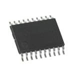
LPC81xM NXP Semiconductors 32-bit ARM Cortex-M0+ microcontroller 4. Ordering information Table 1. Ordering info rmation Type number Package Name Description Version LPC810M021FN8 DIP8 plastic dual in-line package; 8 leads (300 mil) SOT097-2 LPC811M001JDH16 TSSOP16 plastic thin shrink small outline package; 16 leads; body width 4.4 mm SOT403-1 LPC812M101JDH16 TSSOP16 plastic thin shrink small outline package; 16 leads; body width 4.4 mm SOT403-1 LPC812M101JD20 SO20 plastic small outline package; 20 leads; body width 7.5 mm SOT163-1 LPC812M101JDH20 TSSOP20 plastic thin shrink small outline package; 20 leads; body width 4.4 mm SOT360-1 LPC812M101JTB16 XSON16 plastic extremely thin small outline package; no leads; 16 terminals; SOT1341-1 body 2.5 3.2 0.5 mm 4.1 Ordering options Table 2. Ordering opt ions Type number Flash/kB SRAM/kB USART I2C-bus SPI Comparator GPIO Package LPC810M021FN8 4 1 2 1 1 1 6 DIP8 LPC811M001JDH16 8 2 2 1 1 1 14 TSSOP16 LPC812M101JDH16 16 4 3 1 2 1 14 TSSOP16 LPC812M101JD20 16 4 2 1 1 1 18 SO20 LPC812M101JDH20 16 4 3 1 2 1 18 TSSOP20 LPC812M101JTB16 16 4 3 1 2 1 14 XSON16 LPC81XM All information provided in this document is subject to legal disclaimers. © NXP Semiconductors N.V. 2018. All rights reserved. Product data sheet Rev. 4.6 — 4 April 2018 3 of 78
LPC81xM NXP Semiconductors 32-bit ARM Cortex-M0+ microcontroller 5. Marking The LPC81xM devices typically have the following top-side marking: LPC81x xxxxx xxxxxxxx xxYWWxR[x] The last two letters in the last line (field ‘xR’) identify the boot code version and device revision. Table 3. Device revision table Revision identifier (xR) Revision description ‘1A’ Initial device revision with boot code version 13.1 ‘2A’ Device revision with boot code version 13.2 ’4C’ Device revision with boot code version 13.4 Field ‘Y’ states the year the device was manufactured. Field ‘WW’ states the week the device was manufactured during that year. Remark: On the TSSOP16 package, the last line includes only the date code xxYWW. LPC81XM All information provided in this document is subject to legal disclaimers. © NXP Semiconductors N.V. 2018. All rights reserved. Product data sheet Rev. 4.6 — 4 April 2018 4 of 78
LPC81xM NXP Semiconductors 32-bit ARM Cortex-M0+ microcontroller 6. Block diagram (cid:47)(cid:51)(cid:38)(cid:27)(cid:20)(cid:91)(cid:48) (cid:54)(cid:58)(cid:38)(cid:47)(cid:46)(cid:15)(cid:3)(cid:54)(cid:58)(cid:39) (cid:55)(cid:40)(cid:54)(cid:55)(cid:18)(cid:39)(cid:40)(cid:37)(cid:56)(cid:42) (cid:20)(cid:27)(cid:3)(cid:91)(cid:3) (cid:44)(cid:49)(cid:55)(cid:40)(cid:53)(cid:41)(cid:36)(cid:38)(cid:40) (cid:51)(cid:44)(cid:50)(cid:19) (cid:43)(cid:44)(cid:42)(cid:43)(cid:16)(cid:54)(cid:51)(cid:40)(cid:40)(cid:39) (cid:42)(cid:51)(cid:44)(cid:50) (cid:36)(cid:53)(cid:48) (cid:38)(cid:50)(cid:53)(cid:55)(cid:40)(cid:59)(cid:16)(cid:48)(cid:19)(cid:14) (cid:41)(cid:47)(cid:36)(cid:54)(cid:43) (cid:54)(cid:53)(cid:36)(cid:48) (cid:51)(cid:44)(cid:49)(cid:3)(cid:44)(cid:49)(cid:55)(cid:40)(cid:53)(cid:53)(cid:56)(cid:51)(cid:55)(cid:54)(cid:18) (cid:23)(cid:18)(cid:27)(cid:18)(cid:20)(cid:25)(cid:3)(cid:78)(cid:37) (cid:20)(cid:18)(cid:21)(cid:18)(cid:23)(cid:3)(cid:78)(cid:37) (cid:53)(cid:50)(cid:48) (cid:51)(cid:36)(cid:55)(cid:55)(cid:40)(cid:53)(cid:49)(cid:3)(cid:48)(cid:36)(cid:55)(cid:38)(cid:43) (cid:86)(cid:79)(cid:68)(cid:89)(cid:72) (cid:86)(cid:79)(cid:68)(cid:89)(cid:72) (cid:86)(cid:79)(cid:68)(cid:89)(cid:72) (cid:38)(cid:55)(cid:50)(cid:56)(cid:55)(cid:66)(cid:62)(cid:22)(cid:29)(cid:19)(cid:64) (cid:54)(cid:38)(cid:55)(cid:44)(cid:48)(cid:40)(cid:53)(cid:18) (cid:38)(cid:55)(cid:44)(cid:49)(cid:66)(cid:62)(cid:22)(cid:29)(cid:19)(cid:64) (cid:51)(cid:58)(cid:48) (cid:36)(cid:43)(cid:37)(cid:16)(cid:47)(cid:44)(cid:55)(cid:40)(cid:3)(cid:3)(cid:37)(cid:56)(cid:54) (cid:86)(cid:79)(cid:68)(cid:89)(cid:72) (cid:86)(cid:79)(cid:68)(cid:89)(cid:72) (cid:36)(cid:43)(cid:37)(cid:3)(cid:55)(cid:50)(cid:3)(cid:36)(cid:51)(cid:37) (cid:38)(cid:53)(cid:38) (cid:37)(cid:53)(cid:44)(cid:39)(cid:42)(cid:40)(cid:3) (cid:55)(cid:59)(cid:39)(cid:15)(cid:3)(cid:53)(cid:55)(cid:54) (cid:58)(cid:58)(cid:39)(cid:55) (cid:53)(cid:59)(cid:39)(cid:15)(cid:3)(cid:38)(cid:55)(cid:54) (cid:56)(cid:54)(cid:36)(cid:53)(cid:55)(cid:19) (cid:54)(cid:38)(cid:47)(cid:46) (cid:44)(cid:50)(cid:38)(cid:50)(cid:49) (cid:55)(cid:59)(cid:39)(cid:15)(cid:3)(cid:53)(cid:55)(cid:54) (cid:20)(cid:27)(cid:3)(cid:91)(cid:3) (cid:54)(cid:58)(cid:44)(cid:55)(cid:38)(cid:43) (cid:53)(cid:59)(cid:39)(cid:15)(cid:3)(cid:38)(cid:55)(cid:54) (cid:48)(cid:56)(cid:47)(cid:55)(cid:44)(cid:16)(cid:53)(cid:36)(cid:55)(cid:40)(cid:3)(cid:55)(cid:44)(cid:48)(cid:40)(cid:53) (cid:48)(cid:36)(cid:55)(cid:53)(cid:44)(cid:59) (cid:54)(cid:38)(cid:47)(cid:46) (cid:56)(cid:54)(cid:36)(cid:53)(cid:55)(cid:20) (cid:55)(cid:59)(cid:39)(cid:15)(cid:3)(cid:53)(cid:55)(cid:54) (cid:53)(cid:59)(cid:39)(cid:15)(cid:3)(cid:38)(cid:55)(cid:54) (cid:56)(cid:54)(cid:36)(cid:53)(cid:55)(cid:21) (cid:54)(cid:38)(cid:47)(cid:46) (cid:54)(cid:38)(cid:46)(cid:15)(cid:3)(cid:54)(cid:54)(cid:40)(cid:47) (cid:51)(cid:48)(cid:56) (cid:48)(cid:44)(cid:54)(cid:50)(cid:15)(cid:3)(cid:48)(cid:50)(cid:54)(cid:44) (cid:54)(cid:51)(cid:44)(cid:19) (cid:54)(cid:38)(cid:46)(cid:15)(cid:3)(cid:54)(cid:54)(cid:40)(cid:47) (cid:54)(cid:40)(cid:47)(cid:41) (cid:48)(cid:44)(cid:54)(cid:50)(cid:15)(cid:3)(cid:48)(cid:50)(cid:54)(cid:44) (cid:54)(cid:51)(cid:44)(cid:20) (cid:58)(cid:36)(cid:46)(cid:40)(cid:16)(cid:56)(cid:51)(cid:3)(cid:55)(cid:44)(cid:48)(cid:40)(cid:53) (cid:54)(cid:38)(cid:47) (cid:36)(cid:47)(cid:58)(cid:36)(cid:60)(cid:54)(cid:16)(cid:50)(cid:49)(cid:3)(cid:51)(cid:50)(cid:58)(cid:40)(cid:53)(cid:3)(cid:39)(cid:50)(cid:48)(cid:36)(cid:44)(cid:49) (cid:54)(cid:39)(cid:36) (cid:44)(cid:21)(cid:38)(cid:16)(cid:37)(cid:56)(cid:54) (cid:59)(cid:55)(cid:36)(cid:47)(cid:50)(cid:56)(cid:55) (cid:59)(cid:55)(cid:36)(cid:47)(cid:44)(cid:49) (cid:59)(cid:55)(cid:36)(cid:47) (cid:44)(cid:53)(cid:38) (cid:54)(cid:60)(cid:54)(cid:38)(cid:50)(cid:49) (cid:38)(cid:47)(cid:50)(cid:38)(cid:46) (cid:53)(cid:40)(cid:54)(cid:40)(cid:55)(cid:15)(cid:3)(cid:38)(cid:47)(cid:46)(cid:44)(cid:49) (cid:58)(cid:39)(cid:50)(cid:86)(cid:70) (cid:42)(cid:40)(cid:49)(cid:40)(cid:53)(cid:36)(cid:55)(cid:44)(cid:50)(cid:49)(cid:15) (cid:38)(cid:47)(cid:46)(cid:50)(cid:56)(cid:55) (cid:51)(cid:50)(cid:58)(cid:40)(cid:53)(cid:3)(cid:38)(cid:50)(cid:49)(cid:55)(cid:53)(cid:50)(cid:47)(cid:15) (cid:37)(cid:50)(cid:39) (cid:54)(cid:60)(cid:54)(cid:55)(cid:40)(cid:48)(cid:3) (cid:41)(cid:56)(cid:49)(cid:38)(cid:55)(cid:44)(cid:50)(cid:49)(cid:54) (cid:36)(cid:38)(cid:48)(cid:51)(cid:66)(cid:44)(cid:20)(cid:18)(cid:21) (cid:51)(cid:50)(cid:53) (cid:57)(cid:39)(cid:39)(cid:38)(cid:48)(cid:51) (cid:38)(cid:50)(cid:48)(cid:51)(cid:36)(cid:53)(cid:36)(cid:55)(cid:50)(cid:53) (cid:70)(cid:79)(cid:82)(cid:70)(cid:78)(cid:86)(cid:3)(cid:68)(cid:81)(cid:71)(cid:3) (cid:36)(cid:38)(cid:48)(cid:51)(cid:66)(cid:50) (cid:70)(cid:82)(cid:81)(cid:87)(cid:85)(cid:82)(cid:79)(cid:86) (cid:68)(cid:68)(cid:68)(cid:16)(cid:19)(cid:19)(cid:24)(cid:26)(cid:23)(cid:25) Fig 1. LPC81xM block diagram LPC81XM All information provided in this document is subject to legal disclaimers. © NXP Semiconductors N.V. 2018. All rights reserved. Product data sheet Rev. 4.6 — 4 April 2018 5 of 78
LPC81xM NXP Semiconductors 32-bit ARM Cortex-M0+ microcontroller 7. Pinning information 7.1 Pinning (cid:53)(cid:40)(cid:54)(cid:40)(cid:55)(cid:18)(cid:51)(cid:44)(cid:50)(cid:19)(cid:66)(cid:24) (cid:20) (cid:27) (cid:51)(cid:44)(cid:50)(cid:19)(cid:66)(cid:19)(cid:18)(cid:36)(cid:38)(cid:48)(cid:51)(cid:66)(cid:44)(cid:20)(cid:18)(cid:55)(cid:39)(cid:50) (cid:51)(cid:44)(cid:50)(cid:19)(cid:66)(cid:23)(cid:18)(cid:58)(cid:36)(cid:46)(cid:40)(cid:56)(cid:51)(cid:18)(cid:55)(cid:53)(cid:54)(cid:55) (cid:21) (cid:26) (cid:57)(cid:54)(cid:54) (cid:39)(cid:44)(cid:51)(cid:27) (cid:54)(cid:58)(cid:38)(cid:47)(cid:46)(cid:18)(cid:51)(cid:44)(cid:50)(cid:19)(cid:66)(cid:22)(cid:18)(cid:55)(cid:38)(cid:46) (cid:22) (cid:25) (cid:57)(cid:39)(cid:39) (cid:54)(cid:58)(cid:39)(cid:44)(cid:50)(cid:18)(cid:51)(cid:44)(cid:50)(cid:19)(cid:66)(cid:21)(cid:18)(cid:55)(cid:48)(cid:54) (cid:23) (cid:24) (cid:51)(cid:44)(cid:50)(cid:19)(cid:66)(cid:20)(cid:18)(cid:36)(cid:38)(cid:48)(cid:51)(cid:66)(cid:44)(cid:21)(cid:18)(cid:38)(cid:47)(cid:46)(cid:44)(cid:49)(cid:18)(cid:55)(cid:39)(cid:44) (cid:68)(cid:68)(cid:68)(cid:16)(cid:19)(cid:19)(cid:24)(cid:26)(cid:23)(cid:26) Fig 2. Pin configuration DIP8 package (LPC810M021JN8) (cid:51)(cid:44)(cid:50)(cid:19)(cid:66)(cid:20)(cid:22) (cid:20) (cid:20)(cid:25) (cid:51)(cid:44)(cid:50)(cid:19)(cid:66)(cid:19)(cid:18)(cid:36)(cid:38)(cid:48)(cid:51)(cid:66)(cid:44)(cid:20)(cid:18)(cid:55)(cid:39)(cid:50) (cid:51)(cid:44)(cid:50)(cid:19)(cid:66)(cid:20)(cid:21) (cid:21) (cid:20)(cid:24) (cid:51)(cid:44)(cid:50)(cid:19)(cid:66)(cid:25)(cid:18)(cid:57)(cid:39)(cid:39)(cid:38)(cid:48)(cid:51) (cid:53)(cid:40)(cid:54)(cid:40)(cid:55)(cid:18)(cid:51)(cid:44)(cid:50)(cid:19)(cid:66)(cid:24) (cid:22) (cid:20)(cid:23) (cid:51)(cid:44)(cid:50)(cid:19)(cid:66)(cid:26) (cid:51)(cid:44)(cid:50)(cid:19)(cid:66)(cid:23)(cid:18)(cid:58)(cid:36)(cid:46)(cid:40)(cid:56)(cid:51)(cid:18)(cid:55)(cid:53)(cid:54)(cid:55) (cid:23) (cid:55)(cid:54)(cid:54)(cid:50)(cid:51)(cid:20)(cid:25) (cid:20)(cid:22) (cid:57)(cid:54)(cid:54) (cid:54)(cid:58)(cid:38)(cid:47)(cid:46)(cid:18)(cid:51)(cid:44)(cid:50)(cid:19)(cid:66)(cid:22)(cid:18)(cid:55)(cid:38)(cid:46) (cid:24) (cid:20)(cid:21) (cid:57)(cid:39)(cid:39) (cid:54)(cid:58)(cid:39)(cid:44)(cid:50)(cid:18)(cid:51)(cid:44)(cid:50)(cid:19)(cid:66)(cid:21)(cid:18)(cid:55)(cid:48)(cid:54) (cid:25) (cid:20)(cid:20) (cid:51)(cid:44)(cid:50)(cid:19)(cid:66)(cid:27)(cid:18)(cid:59)(cid:55)(cid:36)(cid:47)(cid:44)(cid:49) (cid:51)(cid:44)(cid:50)(cid:19)(cid:66)(cid:20)(cid:20) (cid:26) (cid:20)(cid:19) (cid:51)(cid:44)(cid:50)(cid:19)(cid:66)(cid:28)(cid:18)(cid:59)(cid:55)(cid:36)(cid:47)(cid:50)(cid:56)(cid:55) (cid:51)(cid:44)(cid:50)(cid:19)(cid:66)(cid:20)(cid:19) (cid:27) (cid:28) (cid:51)(cid:44)(cid:50)(cid:19)(cid:66)(cid:20)(cid:18)(cid:36)(cid:38)(cid:48)(cid:51)(cid:66)(cid:44)(cid:21)(cid:18)(cid:38)(cid:47)(cid:46)(cid:44)(cid:49)(cid:18)(cid:55)(cid:39)(cid:44) (cid:68)(cid:68)(cid:68)(cid:16)(cid:19)(cid:19)(cid:22)(cid:26)(cid:19)(cid:26) Fig 3. Pin configuration TSSOP16 package (LPC811M001JDH16 and LPC812M101JDH16) (cid:51)(cid:44)(cid:50)(cid:19)(cid:66)(cid:20)(cid:26) (cid:20) (cid:21)(cid:19) (cid:51)(cid:44)(cid:50)(cid:19)(cid:66)(cid:20)(cid:23) (cid:51)(cid:44)(cid:50)(cid:19)(cid:66)(cid:20)(cid:22) (cid:21) (cid:20)(cid:28) (cid:51)(cid:44)(cid:50)(cid:19)(cid:66)(cid:19)(cid:18)(cid:36)(cid:38)(cid:48)(cid:51)(cid:66)(cid:44)(cid:20)(cid:18)(cid:55)(cid:39)(cid:50) (cid:51)(cid:44)(cid:50)(cid:19)(cid:66)(cid:20)(cid:21) (cid:22) (cid:20)(cid:27) (cid:51)(cid:44)(cid:50)(cid:19)(cid:66)(cid:25)(cid:18)(cid:57)(cid:39)(cid:39)(cid:38)(cid:48)(cid:51) (cid:53)(cid:40)(cid:54)(cid:40)(cid:55)(cid:18)(cid:51)(cid:44)(cid:50)(cid:19)(cid:66)(cid:24) (cid:23) (cid:20)(cid:26) (cid:51)(cid:44)(cid:50)(cid:19)(cid:66)(cid:26) (cid:51)(cid:44)(cid:50)(cid:19)(cid:66)(cid:23)(cid:18)(cid:58)(cid:36)(cid:46)(cid:40)(cid:56)(cid:51)(cid:18)(cid:55)(cid:53)(cid:54)(cid:55) (cid:24) (cid:54)(cid:50)(cid:21)(cid:19) (cid:20)(cid:25) (cid:57)(cid:54)(cid:54) (cid:54)(cid:58)(cid:38)(cid:47)(cid:46)(cid:18)(cid:51)(cid:44)(cid:50)(cid:19)(cid:66)(cid:22)(cid:18)(cid:55)(cid:38)(cid:46) (cid:25) (cid:20)(cid:24) (cid:57)(cid:39)(cid:39) (cid:54)(cid:58)(cid:39)(cid:44)(cid:50)(cid:18)(cid:51)(cid:44)(cid:50)(cid:19)(cid:66)(cid:21)(cid:18)(cid:55)(cid:48)(cid:54) (cid:26) (cid:20)(cid:23) (cid:51)(cid:44)(cid:50)(cid:19)(cid:66)(cid:27)(cid:18)(cid:59)(cid:55)(cid:36)(cid:47)(cid:44)(cid:49) (cid:51)(cid:44)(cid:50)(cid:19)(cid:66)(cid:20)(cid:20) (cid:27) (cid:20)(cid:22) (cid:51)(cid:44)(cid:50)(cid:19)(cid:66)(cid:28)(cid:18)(cid:59)(cid:55)(cid:36)(cid:47)(cid:50)(cid:56)(cid:55) (cid:51)(cid:44)(cid:50)(cid:19)(cid:66)(cid:20)(cid:19) (cid:28) (cid:20)(cid:21) (cid:51)(cid:44)(cid:50)(cid:19)(cid:66)(cid:20)(cid:18)(cid:36)(cid:38)(cid:48)(cid:51)(cid:66)(cid:44)(cid:21)(cid:18)(cid:38)(cid:47)(cid:46)(cid:44)(cid:49)(cid:18)(cid:55)(cid:39)(cid:44) (cid:51)(cid:44)(cid:50)(cid:19)(cid:66)(cid:20)(cid:25) (cid:20)(cid:19) (cid:20)(cid:20) (cid:51)(cid:44)(cid:50)(cid:19)(cid:66)(cid:20)(cid:24) (cid:68)(cid:68)(cid:68)(cid:16)(cid:19)(cid:19)(cid:22)(cid:26)(cid:24)(cid:25) Fig 4. Pin configuration SO20 package (LPC812M101JD20) LPC81XM All information provided in this document is subject to legal disclaimers. © NXP Semiconductors N.V. 2018. All rights reserved. Product data sheet Rev. 4.6 — 4 April 2018 6 of 78
LPC81xM NXP Semiconductors 32-bit ARM Cortex-M0+ microcontroller (cid:51)(cid:44)(cid:50)(cid:19)(cid:66)(cid:20)(cid:26) (cid:20) (cid:21)(cid:19) (cid:51)(cid:44)(cid:50)(cid:19)(cid:66)(cid:20)(cid:23) (cid:51)(cid:44)(cid:50)(cid:19)(cid:66)(cid:20)(cid:22) (cid:21) (cid:20)(cid:28) (cid:51)(cid:44)(cid:50)(cid:19)(cid:66)(cid:19)(cid:18)(cid:36)(cid:38)(cid:48)(cid:51)(cid:66)(cid:44)(cid:20)(cid:18)(cid:55)(cid:39)(cid:50) (cid:51)(cid:44)(cid:50)(cid:19)(cid:66)(cid:20)(cid:21) (cid:22) (cid:20)(cid:27) (cid:51)(cid:44)(cid:50)(cid:19)(cid:66)(cid:25)(cid:18)(cid:57)(cid:39)(cid:39)(cid:38)(cid:48)(cid:51) (cid:53)(cid:40)(cid:54)(cid:40)(cid:55)(cid:18)(cid:51)(cid:44)(cid:50)(cid:19)(cid:66)(cid:24) (cid:23) (cid:20)(cid:26) (cid:51)(cid:44)(cid:50)(cid:19)(cid:66)(cid:26) (cid:51)(cid:44)(cid:50)(cid:19)(cid:66)(cid:23)(cid:18)(cid:58)(cid:36)(cid:46)(cid:40)(cid:56)(cid:51)(cid:18)(cid:55)(cid:53)(cid:54)(cid:55) (cid:24) (cid:55)(cid:54)(cid:54)(cid:50)(cid:51)(cid:21)(cid:19) (cid:20)(cid:25) (cid:57)(cid:54)(cid:54) (cid:54)(cid:58)(cid:38)(cid:47)(cid:46)(cid:18)(cid:51)(cid:44)(cid:50)(cid:19)(cid:66)(cid:22)(cid:18)(cid:55)(cid:38)(cid:46) (cid:25) (cid:20)(cid:24) (cid:57)(cid:39)(cid:39) (cid:54)(cid:58)(cid:39)(cid:44)(cid:50)(cid:18)(cid:51)(cid:44)(cid:50)(cid:19)(cid:66)(cid:21)(cid:18)(cid:55)(cid:48)(cid:54) (cid:26) (cid:20)(cid:23) (cid:51)(cid:44)(cid:50)(cid:19)(cid:66)(cid:27)(cid:18)(cid:59)(cid:55)(cid:36)(cid:47)(cid:44)(cid:49) (cid:51)(cid:44)(cid:50)(cid:19)(cid:66)(cid:20)(cid:20) (cid:27) (cid:20)(cid:22) (cid:51)(cid:44)(cid:50)(cid:19)(cid:66)(cid:28)(cid:18)(cid:59)(cid:55)(cid:36)(cid:47)(cid:50)(cid:56)(cid:55) (cid:51)(cid:44)(cid:50)(cid:19)(cid:66)(cid:20)(cid:19) (cid:28) (cid:20)(cid:21) (cid:51)(cid:44)(cid:50)(cid:19)(cid:66)(cid:20)(cid:18)(cid:36)(cid:38)(cid:48)(cid:51)(cid:66)(cid:44)(cid:21)(cid:18)(cid:38)(cid:47)(cid:46)(cid:44)(cid:49)(cid:18)(cid:55)(cid:39)(cid:44) (cid:51)(cid:44)(cid:50)(cid:19)(cid:66)(cid:20)(cid:25) (cid:20)(cid:19) (cid:20)(cid:20) (cid:51)(cid:44)(cid:50)(cid:19)(cid:66)(cid:20)(cid:24) (cid:68)(cid:68)(cid:68)(cid:16)(cid:19)(cid:19)(cid:22)(cid:26)(cid:26)(cid:24) Fig 5. Pin configuration TSSOP20 package (LPC812M101JDH20) terminal 1 XSON16 index area PIO0_13 1 16 PIO0_0/ACMP_I1/TDO PIO0_12 2 15 PIO0_6/VDDCMP RESET/PIO0_5 3 14 PIO0_7 PIO0_4/WAKEUP/TRST 4 13 VSS SWCLK/PIO0_3/TCK 5 12 VDD SWDIO/PIO0_2/TMS 6 11 PIO0_8/XTALIN PIO0_11 7 10 PIO0_9/XTALOUT PIO0_10 8 9 PIO0_1/ACMP_I2/CLKIN/TDI aaa-009570 Transparent top view Fig 6. Pin configuration XSON16 package (LPC812M101JTB16) LPC81XM All information provided in this document is subject to legal disclaimers. © NXP Semiconductors N.V. 2018. All rights reserved. Product data sheet Rev. 4.6 — 4 April 2018 7 of 78
LPC81xM NXP Semiconductors 32-bit ARM Cortex-M0+ microcontroller 7.2 Pin description The pin description consists of two parts showing pin functions that are fixed to a certain package pin (see Table4) and showing pin functions that can be assigned to any pin on the package through the switch matrix (see Table5). The pin description table in Table4 shows the pin functions that are fixed to specific pins on each package. These fixed-pin functions are selectable between GPIO and the comparator inputs, SWD, RESET, and the XTAL pins. By default, the GPIO function is selected except on pins PIO0_2, PIO0_3, and PIO0_5. JTAG functions are available in boundary scan mode only. Table5 shows the the I2C, USART, SPI, and SCT pin functions, which can be assigned through the switch matrix to any pin that is not power or ground in place of the pin’s fixed functions. The following exceptions apply: For full I2C-bus compatibility, assign the I2C functions to the open-drain pins PIO0_11 and PIO0_10. Do not assign more than one output to any pin. However, more than one input can be assigned to a pin. Once any function is assigned to a pin, the pin’s GPIO functionality is disabled. Pin PIO0_4 triggers a wake-up from Deep power-down mode. If you need to wake up from Deep power-down mode via an external pin, do not assign any movable function to this pin. The JTAG functions TDO, TDI, TCK, TMS, and TRST are selected on pins PIO0_0 to PIO0_4 by hardware when the part is in boundary scan mode. Table 4. Pin descripti on table (fixed pins) Symbol P20 P16 16 Type Rsteasteet Description SO20/TSSO TSSO XSON DIP8 [1] PIO0_0/ACMP_I1/ 19 16 16 8 [5] I/O I; PU PIO0_0 — General purpose digital input/output port 0 pin 0. TDO In ISP mode, this is the USART0 receive pin U0_RXD. In boundary scan mode: TDO (Test Data Out). AI - ACMP_I1 — Analog comparator input 1. PIO0_1/ACMP_I2/ 12 9 9 5 [5] I/O I; PU PIO0_1 — General purpose digital input/output pin. CLKIN/TDI In boundary scan mode: TDI (Test Data In). ISP entry pin on chip versions 1A and 2A and on the DIP8 package (see Table6). For these chip versions and packages, a LOW level on this pin during reset starts the ISP command handler. See PIO0_12 for all other packages. AI - ACMP_I2 — Analog comparator input 2. I - CLKIN — External clock input. LPC81XM All information provided in this document is subject to legal disclaimers. © NXP Semiconductors N.V. 2018. All rights reserved. Product data sheet Rev. 4.6 — 4 April 2018 8 of 78
LPC81xM NXP Semiconductors 32-bit ARM Cortex-M0+ microcontroller Table 4. Pin description table (fixed pins) Symbol P20 P16 16 Type Rsteasteet Description SO20/TSSO TSSO XSON DIP8 [1] SWDIO/PIO0_2/TMS 7 6 6 4 [2] I/O I; PU SWDIO — Serial Wire Debug I/O. SWDIO is enabled by default on this pin. In boundary scan mode: TMS (Test Mode Select). I/O - PIO0_2 — General purpose digital input/output pin. SWCLK/PIO0_3/ 6 5 5 3 [2] I/O I; PU SWCLK — Serial Wire Clock. SWCLK is enabled by default TCK on this pin. In boundary scan mode: TCK (Test Clock). I/O - PIO0_3 — General purpose digital input/output pin. PIO0_4/WAKEUP/ 5 4 4 2 [6] I/O I; PU PIO0_4 — General purpose digital input/output pin. TRST In ISP mode, this is the USART0 transmit pin U0_TXD. In boundary scan mode: TRST (Test Reset). This pin triggers a wake-up from Deep power-down mode. If you need to wake up from Deep power-down mode via an external pin, do not assign any movable function to this pin. This pin should be pulled HIGH externally before entering Deep power-down mode. A LOW-going pulse as short as 50 ns causes the chip to exit Deep power-down mode and wakes up the part. RESET/PIO0_5 4 3 3 1 [4] I/O I; PU RESET — External reset input: A LOW-going pulse as short as 50 ns on this pin resets the device, causing I/O ports and peripherals to take on their default states, and processor execution to begin at address 0. In deep power-down mode, this pin must be pulled HIGH externally. The RESET pin can be left unconnected or be used as a GPIO or for any movable function if an external RESET function is not needed and the Deep power-down mode is not used. I - PIO0_5 — General purpose digital input/output pin. PIO0_6/VDDCMP 18 15 15 - [9] I/O I; PU PIO0_6 — General purpose digital input/output pin. AI - VDDCMP — Alternate reference voltage for the analog comparator. PIO0_7 17 14 14 - [2] I/O I; PU PIO0_7 — General purpose digital input/output pin. PIO0_8/XTALIN 14 11 11 - [8] I/O I; PU PIO0_8 — General purpose digital input/output pin. I - XTALIN — Input to the oscillator circuit and internal clock generator circuits. Input voltage must not exceed 1.95 V. PIO0_9/XTALOUT 13 10 10 - [8] I/O I; PU PIO0_9 — General purpose digital input/output pin. O - XTALOUT — Output from the oscillator circuit. PIO0_10 9 8 8 - [3] I IA PIO0_10 — General purpose digital input/output pin. Assign I2C functions to this pin when true open-drain pins are needed for a signal compliant with the full I2C specification. PIO0_11 8 7 7 - [3] I IA PIO0_11 — General purpose digital input/output pin. Assign I2C functions to this pin when true open-drain pins are needed for a signal compliant with the full I2C specification. LPC81XM All information provided in this document is subject to legal disclaimers. © NXP Semiconductors N.V. 2018. All rights reserved. Product data sheet Rev. 4.6 — 4 April 2018 9 of 78
LPC81xM NXP Semiconductors 32-bit ARM Cortex-M0+ microcontroller Table 4. Pin description table (fixed pins) Symbol P20 P16 16 Type Rsteasteet Description SO20/TSSO TSSO XSON DIP8 [1] PIO0_12 3 2 2 - [2] I/O I; PU PIO0_12 — General purpose digital input/output pin. ISP entry pin on the SO20/TSSOP20/TSSOP16/XSON16 packages starting with chip version 4C (see Table6). A LOW level on this pin during reset starts the ISP command handler. See pin PIO0_1 for the DIP8 package and chip versions 1A and 2A. PIO0_13 2 1 1 - [2] I/O I; PU PIO0_13 — General purpose digital input/output pin. PIO0_14 20 - - - [7] I/O I; PU PIO0_14 — General purpose digital input/output pin. PIO0_15 11 - - - [7] I/O I; PU PIO0_15 — General purpose digital input/output pin. PIO0_16 10 - - - [7] I/O I; PU PIO0_16 — General purpose digital input/output pin. PIO0_17 1 - - - [7] I/O I; PU PIO0_17 — General purpose digital input/output pin. V 15 12 12 6 - - 3.3 V supply voltage. DD V 16 13 13 7 - - Ground. SS [1] Pin state at reset for default function: I = Input; AI = Analog Input; O = Output; PU = internal pull-up enabled (pins pulled up to full V DD level); IA = inactive, no pull-up/down enabled. [2] 5 V tolerant pad providing digital I/O functions with configurable pull-up/pull-down resistors and configurable hysteresis; includes high-current output driver. [3] True open-drain pin. I2C-bus pins compliant with the I2C-bus specification for I2C standard mode, I2C Fast-mode, and I2C Fast-mode Plus. Do not use this pad for high-speed applications such as SPI or USART. The pin requires an external pull-up to provide output functionality. When power is switched off, this pin is floating and does not disturb the I2C lines. Open-drain configuration applies to all functions on this pin. Remark: If this pin is not available on the package, prevent it from internally floating as follows: Set bits 10 and 11 in the GPIO DIR0 register to 1 to enable the output driver and write 1 to bits 10 and 11 in the GPIO CLR0 register to drive the outputs LOW internally. [4] See Figure11 for the reset pad configuration. RESET functionality is not available in Deep power-down mode. Use the WAKEUP pin to reset the chip and wake up from Deep power-down mode. An external pull-up resistor is required on this pin for the Deep power-down mode. [5] 5 V tolerant pin providing standard digital I/O functions with configurable modes, configurable hysteresis, and analog input. When configured as an analog input, the digital section of the pin is disabled, and the pin is not 5 V tolerant. [6] 5 V tolerant pad providing digital I/O functions with configurable pull-up/pull-down resistors and configurable hysteresis. In Deep power-down mode, pulling this pin LOW wakes up the chip. The wake-up pin function can be disabled and the pin can be used for other purposes, if the WKT low power oscillator is enabled for waking up the part from Deep power-down mode. [7] 5 V tolerant pad providing digital I/O functions with configurable pull-up/pull-down resistors and configurable hysteresis. [8] 5 V tolerant pin providing standard digital I/O functions with configurable modes, configurable hysteresis, and analog I/O for the system oscillator. When configured as an analog I/O, the digital section of the pin is disabled, and the pin is not 5 V tolerant. [9] The digital part of this pin is 3 V tolerant pin due to special analog functionality. Pin provides standard digital I/O functions with configurable modes, configurable hysteresis, and an analog input. When configured as an analog input, the digital section of the pin is disabled. Table 5. Movable functions (assign to pins PIO0_0 to PIO_17 through switch matrix) Function name Type Description U0_TXD O Transmitter output for USART0. U0_RXD I Receiver input for USART0. U0_RTS O Request To Send output for USART0. U0_CTS I Clear To Send input for USART0. LPC81XM All information provided in this document is subject to legal disclaimers. © NXP Semiconductors N.V. 2018. All rights reserved. Product data sheet Rev. 4.6 — 4 April 2018 10 of 78
LPC81xM NXP Semiconductors 32-bit ARM Cortex-M0+ microcontroller Table 5. Movable functions (assign to pins PIO0_0 to PIO_17 through switch matrix) Function name Type Description U0_SCLK I/O Serial clock input/output for USART0 in synchronous mode. U1_TXD O Transmitter output for USART1. U1_RXD I Receiver input for USART1. U1_RTS O Request To Send output for USART1. U1_CTS I Clear To Send input for USART1. U1_SCLK I/O Serial clock input/output for USART1 in synchronous mode. U2_TXD O Transmitter output for USART2. U2_RXD I Receiver input for USART2. U2_RTS O Request To Send output for USART2. U2_CTS I Clear To Send input for USART2. U2_SCLK I/O Serial clock input/output for USART2 in synchronous mode. SPI0_SCK I/O Serial clock for SPI0. SPI0_MOSI I/O Master Out Slave In for SPI0. SPI0_MISO I/O Master In Slave Out for SPI0. SPI0_SSEL I/O Slave select for SPI0. SPI1_SCK I/O Serial clock for SPI1. SPI1_MOSI I/O Master Out Slave In for SPI1. SPI1_MISO I/O Master In Slave Out for SPI1. SPI1_SSEL I/O Slave select for SPI1. CTIN_0 I SCT input 0. CTIN_1 I SCT input 1. CTIN_2 I SCT input 2. CTIN_3 I SCT input 3. CTOUT_0 O SCT output 0. CTOUT_1 O SCT output 1. CTOUT_2 O SCT output 2. CTOUT_3 O SCT output 3. I2C0_SCL I/O I2C-bus clock input/output (open-drain if assigned to pin PIO0_10). High-current sink only if assigned to PIO0_10 and if I2C Fast-mode Plus is selected in the I/O configuration register. I2C0_SDA I/O I2C-bus data input/output (open-drain if assigned to pin PIO0_11). High-current sink only if assigned to pin PIO0_11 and if I2C Fast-mode Plus is selected in the I/O configuration register. ACMP_O O Analog comparator digital output. CLKOUT O Clock output. GPIO_INT_BMAT O Output of the pattern match engine. LPC81XM All information provided in this document is subject to legal disclaimers. © NXP Semiconductors N.V. 2018. All rights reserved. Product data sheet Rev. 4.6 — 4 April 2018 11 of 78
LPC81xM NXP Semiconductors 32-bit ARM Cortex-M0+ microcontroller Table 6. Pin location in ISP mode ISP entry pin USART RXD USART TXD Marking Boot loader Package version PIO0_1 PIO0_0 PIO0_4 1A v 13.1 TSSOP20; SO20; TSSOP16; DIP8; XSON16 PIO0_1 PIO0_0 PIO0_4 2A v 13.2 TSSOP20; SO20; TSSOP16; DIP8; XSON16 PIO0_1 PIO0_0 PIO0_4 4C and v 13.4 and DIP8 later later PIO0_12 PIO0_0 PIO0_4 4C and v 13.4 and TSSOP20; SO20; later later TSSOP16; XSON16 LPC81XM All information provided in this document is subject to legal disclaimers. © NXP Semiconductors N.V. 2018. All rights reserved. Product data sheet Rev. 4.6 — 4 April 2018 12 of 78
LPC81xM NXP Semiconductors 32-bit ARM Cortex-M0+ microcontroller 8. Functional description 8.1 ARM Cortex-M0+ core The ARM Cortex-M0+ core runs at an operating frequency of up to 30 MHz using a two-stage pipeline. Integrated in the core are the NVIC and Serial Wire Debug with four breakpoints and two watchpoints. The ARM Cortex-M0+ core supports a single-cycle I/O enabled port for fast GPIO access. The core includes a single-cycle multiplier and a system tick timer. 8.2 On-chip flash program memory The LPC81xM contain up to 16 kB of on-chip flash program memory. The flash memory supports a 64 Byte page size with page write and erase. 8.3 On-chip SRAM The LPC81xM contain a total of up to 4 kB on-chip static RAM data memory. 8.4 On-chip ROM The 8 kB on-chip ROM contains the boot loader and the following Application Programming Interfaces (API): • In-System Programming (ISP) and In-Application Programming (IAP) support for flash programming • Power profiles for configuring power consumption and PLL settings • USART driver API routines • I2C-bus driver API routines 8.5 Nested Vectored Interrupt Controller (NVIC) The Nested Vectored Interrupt Controller (NVIC) is an integral part of the Cortex-M0+. The tight coupling to the CPU allows for low interrupt latency and efficient processing of late arriving interrupts. 8.5.1 Features • Controls system exceptions and peripheral interrupts. • On the LPC81xM, the NVIC supports 32 vectored interrupts including up to 8 external interrupt inputs selectable from all GPIO pins. • Four programmable interrupt priority levels with hardware priority level masking. • Software interrupt generation using the ARM exceptions SVCall and PendSV. • Relocatable interrupt vector table using vector table offset register. 8.5.2 Interrupt sources Each peripheral device has one interrupt line connected to the NVIC but may have several interrupt flags. Individual interrupt flags may also represent more than one interrupt source. LPC81XM All information provided in this document is subject to legal disclaimers. © NXP Semiconductors N.V. 2018. All rights reserved. Product data sheet Rev. 4.6 — 4 April 2018 13 of 78
LPC81xM NXP Semiconductors 32-bit ARM Cortex-M0+ microcontroller Up to eight pins, regardless of the selected function, can be programmed to generate an interrupt on a level, a rising or falling edge, or both. The interrupt generating pins can be selected from all digital or mixed digital/analog pins. The pin interrupt/pattern match block controls the edge or level detection mechanism. 8.6 System tick timer The ARM Cortex-M0+ includes a 24-bit system tick timer (SysTick) that is intended to generate a dedicated SysTick exception at a fixed time interval (typically 10 ms). 8.7 Memory map The LPC81xM incorporates several distinct memory regions. Figure7 shows the overall map of the entire address space from the user program viewpoint following reset. The interrupt vector area supports address remapping. The ARM private peripheral bus includes the ARM core registers for controlling the NVIC, the system tick timer (SysTick), and the reduced power modes. LPC81XM All information provided in this document is subject to legal disclaimers. © NXP Semiconductors N.V. 2018. All rights reserved. Product data sheet Rev. 4.6 — 4 April 2018 14 of 78
LPC81xM NXP Semiconductors 32-bit ARM Cortex-M0+ microcontroller (cid:36)(cid:51)(cid:37)(cid:3)(cid:83)(cid:72)(cid:85)(cid:76)(cid:83)(cid:75)(cid:72)(cid:85)(cid:68)(cid:79)(cid:86) (cid:19)(cid:91)(cid:23)(cid:19)(cid:19)(cid:27)(cid:3)(cid:19)(cid:19)(cid:19)(cid:19) (cid:47)(cid:51)(cid:38)(cid:27)(cid:20)(cid:91)(cid:48) (cid:23)(cid:3)(cid:42)(cid:37) (cid:19)(cid:91)(cid:41)(cid:41)(cid:41)(cid:41)(cid:3)(cid:41)(cid:41)(cid:41)(cid:41) (cid:22)(cid:20)(cid:3)(cid:16)(cid:3)(cid:21)(cid:27)(cid:3)(cid:85)(cid:72)(cid:86)(cid:72)(cid:85)(cid:89)(cid:72)(cid:71) (cid:85)(cid:72)(cid:86)(cid:72)(cid:85)(cid:89)(cid:72)(cid:71) (cid:19)(cid:91)(cid:40)(cid:19)(cid:20)(cid:19)(cid:3)(cid:19)(cid:19)(cid:19)(cid:19) (cid:19)(cid:91)(cid:23)(cid:19)(cid:19)(cid:26)(cid:3)(cid:19)(cid:19)(cid:19)(cid:19) (cid:83)(cid:85)(cid:76)(cid:89)(cid:68)(cid:87)(cid:72)(cid:3)(cid:83)(cid:72)(cid:85)(cid:76)(cid:83)(cid:75)(cid:72)(cid:85)(cid:68)(cid:79)(cid:3)(cid:69)(cid:88)(cid:86) (cid:21)(cid:26) (cid:19)(cid:91)(cid:40)(cid:19)(cid:19)(cid:19)(cid:3)(cid:19)(cid:19)(cid:19)(cid:19) (cid:56)(cid:54)(cid:36)(cid:53)(cid:55)(cid:21) (cid:19)(cid:91)(cid:23)(cid:19)(cid:19)(cid:25)(cid:3)(cid:38)(cid:19)(cid:19)(cid:19) (cid:21)(cid:25) (cid:56)(cid:54)(cid:36)(cid:53)(cid:55)(cid:20) (cid:85)(cid:72)(cid:86)(cid:72)(cid:85)(cid:89)(cid:72)(cid:71) (cid:19)(cid:91)(cid:23)(cid:19)(cid:19)(cid:25)(cid:3)(cid:27)(cid:19)(cid:19)(cid:19) (cid:19)(cid:91)(cid:36)(cid:19)(cid:19)(cid:19)(cid:3)(cid:27)(cid:19)(cid:19)(cid:19) (cid:21)(cid:24) (cid:56)(cid:54)(cid:36)(cid:53)(cid:55)(cid:19) (cid:19)(cid:91)(cid:23)(cid:19)(cid:19)(cid:25)(cid:3)(cid:23)(cid:19)(cid:19)(cid:19) (cid:83)(cid:76)(cid:81)(cid:3)(cid:76)(cid:81)(cid:87)(cid:72)(cid:85)(cid:85)(cid:88)(cid:83)(cid:87)(cid:86)(cid:18)(cid:83)(cid:68)(cid:87)(cid:87)(cid:72)(cid:85)(cid:81)(cid:3)(cid:80)(cid:68)(cid:87)(cid:70)(cid:75) (cid:19)(cid:91)(cid:36)(cid:19)(cid:19)(cid:19)(cid:3)(cid:23)(cid:19)(cid:19)(cid:19) (cid:21)(cid:23) (cid:85)(cid:72)(cid:86)(cid:72)(cid:85)(cid:89)(cid:72)(cid:71) (cid:19)(cid:91)(cid:23)(cid:19)(cid:19)(cid:25)(cid:3)(cid:19)(cid:19)(cid:19)(cid:19) (cid:42)(cid:51)(cid:44)(cid:50) (cid:21)(cid:22) (cid:54)(cid:51)(cid:44)(cid:20) (cid:19)(cid:91)(cid:23)(cid:19)(cid:19)(cid:24)(cid:3)(cid:38)(cid:19)(cid:19)(cid:19) (cid:19)(cid:91)(cid:36)(cid:19)(cid:19)(cid:19)(cid:3)(cid:19)(cid:19)(cid:19)(cid:19) (cid:85)(cid:72)(cid:86)(cid:72)(cid:85)(cid:89)(cid:72)(cid:71) (cid:21)(cid:21) (cid:54)(cid:51)(cid:44)(cid:19) (cid:19)(cid:91)(cid:23)(cid:19)(cid:19)(cid:24)(cid:3)(cid:27)(cid:19)(cid:19)(cid:19) (cid:19)(cid:91)(cid:24)(cid:19)(cid:19)(cid:19)(cid:3)(cid:27)(cid:19)(cid:19)(cid:19) (cid:21)(cid:20) (cid:85)(cid:72)(cid:86)(cid:72)(cid:85)(cid:89)(cid:72)(cid:71) (cid:19)(cid:91)(cid:23)(cid:19)(cid:19)(cid:24)(cid:3)(cid:23)(cid:19)(cid:19)(cid:19) (cid:54)(cid:38)(cid:55)(cid:76)(cid:80)(cid:72)(cid:85)(cid:18)(cid:51)(cid:58)(cid:48) (cid:21)(cid:19) (cid:44)(cid:21)(cid:38) (cid:19)(cid:91)(cid:24)(cid:19)(cid:19)(cid:19)(cid:3)(cid:23)(cid:19)(cid:19)(cid:19) (cid:19)(cid:91)(cid:23)(cid:19)(cid:19)(cid:24)(cid:3)(cid:19)(cid:19)(cid:19)(cid:19) (cid:38)(cid:53)(cid:38) (cid:20)(cid:28) (cid:85)(cid:72)(cid:86)(cid:72)(cid:85)(cid:89)(cid:72)(cid:71) (cid:19)(cid:91)(cid:24)(cid:19)(cid:19)(cid:19)(cid:3)(cid:19)(cid:19)(cid:19)(cid:19) (cid:19)(cid:91)(cid:23)(cid:19)(cid:19)(cid:23)(cid:3)(cid:38)(cid:19)(cid:19)(cid:19) (cid:20)(cid:27) (cid:54)(cid:60)(cid:54)(cid:38)(cid:50)(cid:49) (cid:19)(cid:91)(cid:23)(cid:19)(cid:19)(cid:23)(cid:3)(cid:27)(cid:19)(cid:19)(cid:19) (cid:85)(cid:72)(cid:86)(cid:72)(cid:85)(cid:89)(cid:72)(cid:71) (cid:20)(cid:26) (cid:44)(cid:50)(cid:38)(cid:50)(cid:49) (cid:19)(cid:91)(cid:23)(cid:19)(cid:19)(cid:23)(cid:3)(cid:23)(cid:19)(cid:19)(cid:19) (cid:19)(cid:91)(cid:23)(cid:19)(cid:19)(cid:27)(cid:3)(cid:19)(cid:19)(cid:19)(cid:19) (cid:36)(cid:51)(cid:37)(cid:3)(cid:83)(cid:72)(cid:85)(cid:76)(cid:83)(cid:75)(cid:72)(cid:85)(cid:68)(cid:79)(cid:86) (cid:20)(cid:25) (cid:73)(cid:79)(cid:68)(cid:86)(cid:75)(cid:3)(cid:70)(cid:82)(cid:81)(cid:87)(cid:85)(cid:82)(cid:79)(cid:79)(cid:72)(cid:85) (cid:19)(cid:91)(cid:23)(cid:19)(cid:19)(cid:23)(cid:3)(cid:19)(cid:19)(cid:19)(cid:19) (cid:20)(cid:3)(cid:42)(cid:37) (cid:19)(cid:91)(cid:23)(cid:19)(cid:19)(cid:19)(cid:3)(cid:19)(cid:19)(cid:19)(cid:19) (cid:20)(cid:24) (cid:85)(cid:72)(cid:86)(cid:72)(cid:85)(cid:89)(cid:72)(cid:71) (cid:19)(cid:91)(cid:23)(cid:19)(cid:19)(cid:22)(cid:3)(cid:38)(cid:19)(cid:19)(cid:19) (cid:20)(cid:23) (cid:85)(cid:72)(cid:86)(cid:72)(cid:85)(cid:89)(cid:72)(cid:71) (cid:19)(cid:91)(cid:23)(cid:19)(cid:19)(cid:22)(cid:3)(cid:27)(cid:19)(cid:19)(cid:19) (cid:85)(cid:72)(cid:86)(cid:72)(cid:85)(cid:89)(cid:72)(cid:71) (cid:20)(cid:22) (cid:85)(cid:72)(cid:86)(cid:72)(cid:85)(cid:89)(cid:72)(cid:71) (cid:19)(cid:17)(cid:24)(cid:3)(cid:42)(cid:37) (cid:19)(cid:91)(cid:21)(cid:19)(cid:19)(cid:19)(cid:3)(cid:19)(cid:19)(cid:19)(cid:19) (cid:19)(cid:91)(cid:23)(cid:19)(cid:19)(cid:22)(cid:3)(cid:23)(cid:19)(cid:19)(cid:19) (cid:85)(cid:72)(cid:86)(cid:72)(cid:85)(cid:89)(cid:72)(cid:71) (cid:20)(cid:21) (cid:85)(cid:72)(cid:86)(cid:72)(cid:85)(cid:89)(cid:72)(cid:71) (cid:19)(cid:91)(cid:23)(cid:19)(cid:19)(cid:22)(cid:3)(cid:19)(cid:19)(cid:19)(cid:19) (cid:19)(cid:91)(cid:20)(cid:41)(cid:41)(cid:41)(cid:3)(cid:21)(cid:19)(cid:19)(cid:19) (cid:20)(cid:20) (cid:85)(cid:72)(cid:86)(cid:72)(cid:85)(cid:89)(cid:72)(cid:71) (cid:27)(cid:3)(cid:78)(cid:37)(cid:3)(cid:69)(cid:82)(cid:82)(cid:87)(cid:3)(cid:53)(cid:50)(cid:48) (cid:19)(cid:91)(cid:23)(cid:19)(cid:19)(cid:21)(cid:3)(cid:38)(cid:19)(cid:19)(cid:19) (cid:19)(cid:91)(cid:20)(cid:41)(cid:41)(cid:41)(cid:3)(cid:19)(cid:19)(cid:19)(cid:19) (cid:20)(cid:19) (cid:85)(cid:72)(cid:86)(cid:72)(cid:85)(cid:89)(cid:72)(cid:71) (cid:19)(cid:91)(cid:23)(cid:19)(cid:19)(cid:21)(cid:3)(cid:27)(cid:19)(cid:19)(cid:19) (cid:85)(cid:72)(cid:86)(cid:72)(cid:85)(cid:89)(cid:72)(cid:71) (cid:28) (cid:68)(cid:81)(cid:68)(cid:79)(cid:82)(cid:74)(cid:3)(cid:70)(cid:82)(cid:80)(cid:83)(cid:68)(cid:85)(cid:68)(cid:87)(cid:82)(cid:85) (cid:19)(cid:91)(cid:23)(cid:19)(cid:19)(cid:21)(cid:3)(cid:23)(cid:19)(cid:19)(cid:19) (cid:19)(cid:91)(cid:20)(cid:23)(cid:19)(cid:19)(cid:3)(cid:19)(cid:23)(cid:19)(cid:19) (cid:20)(cid:3)(cid:78)(cid:37)(cid:3)(cid:48)(cid:55)(cid:37)(cid:3)(cid:85)(cid:72)(cid:74)(cid:76)(cid:86)(cid:87)(cid:72)(cid:85)(cid:86) (cid:27) (cid:51)(cid:48)(cid:56) (cid:19)(cid:91)(cid:23)(cid:19)(cid:19)(cid:21)(cid:3)(cid:19)(cid:19)(cid:19)(cid:19) (cid:19)(cid:91)(cid:20)(cid:23)(cid:19)(cid:19)(cid:3)(cid:19)(cid:19)(cid:19)(cid:19) (cid:26) (cid:85)(cid:72)(cid:86)(cid:72)(cid:85)(cid:89)(cid:72)(cid:71) (cid:19)(cid:91)(cid:23)(cid:19)(cid:19)(cid:20)(cid:3)(cid:38)(cid:19)(cid:19)(cid:19) (cid:85)(cid:72)(cid:86)(cid:72)(cid:85)(cid:89)(cid:72)(cid:71) (cid:25) (cid:85)(cid:72)(cid:86)(cid:72)(cid:85)(cid:89)(cid:72)(cid:71) (cid:19)(cid:91)(cid:23)(cid:19)(cid:19)(cid:20)(cid:3)(cid:27)(cid:19)(cid:19)(cid:19) (cid:23)(cid:3)(cid:78)(cid:37)(cid:3)(cid:3)(cid:54)(cid:53)(cid:36)(cid:48)(cid:3)(cid:11)(cid:47)(cid:51)(cid:38)(cid:27)(cid:20)(cid:21)(cid:12) (cid:19)(cid:91)(cid:20)(cid:19)(cid:19)(cid:19)(cid:3)(cid:20)(cid:19)(cid:19)(cid:19) (cid:24) (cid:85)(cid:72)(cid:86)(cid:72)(cid:85)(cid:89)(cid:72)(cid:71) (cid:19)(cid:91)(cid:23)(cid:19)(cid:19)(cid:20)(cid:3)(cid:23)(cid:19)(cid:19)(cid:19) (cid:19)(cid:91)(cid:20)(cid:19)(cid:19)(cid:19)(cid:3)(cid:19)(cid:27)(cid:19)(cid:19) (cid:85)(cid:72)(cid:86)(cid:72)(cid:85)(cid:89)(cid:72)(cid:71) (cid:21)(cid:3)(cid:78)(cid:37)(cid:3)(cid:3)(cid:54)(cid:53)(cid:36)(cid:48)(cid:3)(cid:11)(cid:47)(cid:51)(cid:38)(cid:27)(cid:20)(cid:20)(cid:12) (cid:23) (cid:19)(cid:91)(cid:23)(cid:19)(cid:19)(cid:20)(cid:3)(cid:19)(cid:19)(cid:19)(cid:19) (cid:20)(cid:3)(cid:78)(cid:37)(cid:3)(cid:3)(cid:54)(cid:53)(cid:36)(cid:48)(cid:3)(cid:11)(cid:47)(cid:51)(cid:38)(cid:27)(cid:20)(cid:19)(cid:12) (cid:19)(cid:91)(cid:20)(cid:19)(cid:19)(cid:19)(cid:3)(cid:19)(cid:23)(cid:19)(cid:19) (cid:22) (cid:86)(cid:90)(cid:76)(cid:87)(cid:70)(cid:75)(cid:3)(cid:80)(cid:68)(cid:87)(cid:85)(cid:76)(cid:91) (cid:19)(cid:91)(cid:23)(cid:19)(cid:19)(cid:19)(cid:3)(cid:38)(cid:19)(cid:19)(cid:19) (cid:19)(cid:91)(cid:20)(cid:19)(cid:19)(cid:19)(cid:3)(cid:19)(cid:19)(cid:19)(cid:19) (cid:21) (cid:3)(cid:86)(cid:72)(cid:79)(cid:73)(cid:3)(cid:90)(cid:68)(cid:78)(cid:72)(cid:16)(cid:88)(cid:83)(cid:3)(cid:87)(cid:76)(cid:80)(cid:72)(cid:85) (cid:19)(cid:91)(cid:23)(cid:19)(cid:19)(cid:19)(cid:3)(cid:27)(cid:19)(cid:19)(cid:19) (cid:85)(cid:72)(cid:86)(cid:72)(cid:85)(cid:89)(cid:72)(cid:71) (cid:20) (cid:48)(cid:53)(cid:55) (cid:19)(cid:91)(cid:23)(cid:19)(cid:19)(cid:19)(cid:3)(cid:23)(cid:19)(cid:19)(cid:19) (cid:19)(cid:91)(cid:19)(cid:19)(cid:19)(cid:19)(cid:3)(cid:23)(cid:19)(cid:19)(cid:19) (cid:19) (cid:58)(cid:58)(cid:39)(cid:55) (cid:19)(cid:91)(cid:23)(cid:19)(cid:19)(cid:19)(cid:3)(cid:19)(cid:19)(cid:19)(cid:19) (cid:20)(cid:25)(cid:3)(cid:78)(cid:37)(cid:3)(cid:82)(cid:81)(cid:16)(cid:70)(cid:75)(cid:76)(cid:83)(cid:3)(cid:73)(cid:79)(cid:68)(cid:86)(cid:75)(cid:3)(cid:11)(cid:47)(cid:51)(cid:38)(cid:27)(cid:20)(cid:21)(cid:12) (cid:19)(cid:91)(cid:19)(cid:19)(cid:19)(cid:19)(cid:3)(cid:21)(cid:19)(cid:19)(cid:19) (cid:27)(cid:3)(cid:78)(cid:37)(cid:3)(cid:82)(cid:81)(cid:16)(cid:70)(cid:75)(cid:76)(cid:83)(cid:3)(cid:73)(cid:79)(cid:68)(cid:86)(cid:75)(cid:3)(cid:11)(cid:47)(cid:51)(cid:38)(cid:27)(cid:20)(cid:20)(cid:12) (cid:19)(cid:91)(cid:19)(cid:19)(cid:19)(cid:19)(cid:3)(cid:19)(cid:19)(cid:38)(cid:19) (cid:19)(cid:91)(cid:19)(cid:19)(cid:19)(cid:19)(cid:3)(cid:20)(cid:19)(cid:19)(cid:19) (cid:68)(cid:70)(cid:87)(cid:76)(cid:89)(cid:72)(cid:3)(cid:76)(cid:81)(cid:87)(cid:72)(cid:85)(cid:85)(cid:88)(cid:83)(cid:87)(cid:3)(cid:89)(cid:72)(cid:70)(cid:87)(cid:82)(cid:85)(cid:86) (cid:23)(cid:3)(cid:78)(cid:37)(cid:3)(cid:82)(cid:81)(cid:16)(cid:70)(cid:75)(cid:76)(cid:83)(cid:3)(cid:73)(cid:79)(cid:68)(cid:86)(cid:75)(cid:3)(cid:11)(cid:47)(cid:51)(cid:38)(cid:27)(cid:20)(cid:19)(cid:12) (cid:19)(cid:91)(cid:19)(cid:19)(cid:19)(cid:19)(cid:3)(cid:19)(cid:19)(cid:19)(cid:19) (cid:19)(cid:3)(cid:42)(cid:37) (cid:19)(cid:91)(cid:19)(cid:19)(cid:19)(cid:19)(cid:3)(cid:19)(cid:19)(cid:19)(cid:19) (cid:68)(cid:68)(cid:68)(cid:16)(cid:19)(cid:19)(cid:24)(cid:26)(cid:23)(cid:27) Fig 7. LPC81xM Memory map 8.8 I/O configuration The IOCON block controls the configuration of the I/O pins. Each digital or mixed digital/analog pin with the PIO0_n designator (except the true open-drain pins PIO0_10 and PIO0_11) in Table4 can be configured as follows: • Enable or disable the weak internal pull-up and pull-down resistors. • Select a pseudo open-drain mode. The input cannot be pulled up above V . This pin DD is not 5 V tolerant when V = 0. DD LPC81XM All information provided in this document is subject to legal disclaimers. © NXP Semiconductors N.V. 2018. All rights reserved. Product data sheet Rev. 4.6 — 4 April 2018 15 of 78
LPC81xM NXP Semiconductors 32-bit ARM Cortex-M0+ microcontroller • Program the input glitch filter with different filter constants using one of the IOCON divided clock signals (IOCONCLKCDIV, see Figure 10 “LPC81xM clock generation”). You can also bypass the glitch filter. • Invert the input signal. • Hysteresis can be enabled or disabled. • For pins PIO0_10 and PIO0_11, select the I2C-mode and output driver for standard digital operation, for I2C standard and fast modes, or for I2C Fast mode+. • On mixed digital/analog pins, enable the analog input mode. Enabling the analog mode disconnects the digital functionality. Remark: The functionality of each I/O pin is flexible and is determined entirely through the switch matrix. See Section8.9 for details. 8.8.1 Standard I/O pad configuration Figure8 shows the possible pin modes for standard I/O pins with analog input function: • Digital output driver with configurable open-drain output • Digital input: Weak pull-up resistor (PMOS device) enabled/disabled • Digital input: Weak pull-down resistor (NMOS device) enabled/disabled • Digital input: Repeater mode enabled/disabled • Digital input: Input glitch filter selectable on all pins • Analog input LPC81XM All information provided in this document is subject to legal disclaimers. © NXP Semiconductors N.V. 2018. All rights reserved. Product data sheet Rev. 4.6 — 4 April 2018 16 of 78
LPC81xM NXP Semiconductors 32-bit ARM Cortex-M0+ microcontroller (cid:57)(cid:39)(cid:39) (cid:57)(cid:39)(cid:39) (cid:82)(cid:83)(cid:72)(cid:81)(cid:16)(cid:71)(cid:85)(cid:68)(cid:76)(cid:81)(cid:3)(cid:72)(cid:81)(cid:68)(cid:69)(cid:79)(cid:72) (cid:86)(cid:87)(cid:85)(cid:82)(cid:81)(cid:74) (cid:83)(cid:76)(cid:81)(cid:3)(cid:70)(cid:82)(cid:81)(cid:73)(cid:76)(cid:74)(cid:88)(cid:85)(cid:72)(cid:71) (cid:82)(cid:88)(cid:87)(cid:83)(cid:88)(cid:87)(cid:3)(cid:72)(cid:81)(cid:68)(cid:69)(cid:79)(cid:72) (cid:40)(cid:54)(cid:39) (cid:83)(cid:88)(cid:79)(cid:79)(cid:16)(cid:88)(cid:83) (cid:68)(cid:86)(cid:3)(cid:71)(cid:76)(cid:74)(cid:76)(cid:87)(cid:68)(cid:79)(cid:3)(cid:82)(cid:88)(cid:87)(cid:83)(cid:88)(cid:87) (cid:71)(cid:85)(cid:76)(cid:89)(cid:72)(cid:85) (cid:71)(cid:68)(cid:87)(cid:68)(cid:3)(cid:82)(cid:88)(cid:87)(cid:83)(cid:88)(cid:87) (cid:51)(cid:44)(cid:49) (cid:86)(cid:87)(cid:85)(cid:82)(cid:81)(cid:74) (cid:83)(cid:88)(cid:79)(cid:79)(cid:16)(cid:71)(cid:82)(cid:90)(cid:81) (cid:40)(cid:54)(cid:39) (cid:57)(cid:54)(cid:54) (cid:57)(cid:39)(cid:39) (cid:90)(cid:72)(cid:68)(cid:78) (cid:83)(cid:88)(cid:79)(cid:79)(cid:16)(cid:88)(cid:83) (cid:83)(cid:88)(cid:79)(cid:79)(cid:16)(cid:88)(cid:83)(cid:3)(cid:72)(cid:81)(cid:68)(cid:69)(cid:79)(cid:72) (cid:90)(cid:72)(cid:68)(cid:78) (cid:85)(cid:72)(cid:83)(cid:72)(cid:68)(cid:87)(cid:72)(cid:85)(cid:3)(cid:80)(cid:82)(cid:71)(cid:72) (cid:83)(cid:76)(cid:81)(cid:3)(cid:70)(cid:82)(cid:81)(cid:73)(cid:76)(cid:74)(cid:88)(cid:85)(cid:72)(cid:71) (cid:72)(cid:81)(cid:68)(cid:69)(cid:79)(cid:72) (cid:83)(cid:88)(cid:79)(cid:79)(cid:16)(cid:71)(cid:82)(cid:90)(cid:81) (cid:68)(cid:86)(cid:3)(cid:71)(cid:76)(cid:74)(cid:76)(cid:87)(cid:68)(cid:79)(cid:3)(cid:76)(cid:81)(cid:83)(cid:88)(cid:87) (cid:83)(cid:88)(cid:79)(cid:79)(cid:16)(cid:71)(cid:82)(cid:90)(cid:81)(cid:3)(cid:72)(cid:81)(cid:68)(cid:69)(cid:79)(cid:72) (cid:71)(cid:68)(cid:87)(cid:68)(cid:3)(cid:76)(cid:81)(cid:83)(cid:88)(cid:87) (cid:51)(cid:53)(cid:50)(cid:42)(cid:53)(cid:36)(cid:48)(cid:48)(cid:36)(cid:37)(cid:47)(cid:40) (cid:42)(cid:47)(cid:44)(cid:55)(cid:38)(cid:43)(cid:3)(cid:41)(cid:44)(cid:47)(cid:55)(cid:40)(cid:53) (cid:86)(cid:72)(cid:79)(cid:72)(cid:70)(cid:87)(cid:3)(cid:71)(cid:68)(cid:87)(cid:68) (cid:76)(cid:81)(cid:89)(cid:72)(cid:85)(cid:87)(cid:72)(cid:85) (cid:86)(cid:72)(cid:79)(cid:72)(cid:70)(cid:87)(cid:3)(cid:74)(cid:79)(cid:76)(cid:87)(cid:70)(cid:75) (cid:73)(cid:76)(cid:79)(cid:87)(cid:72)(cid:85) (cid:86)(cid:72)(cid:79)(cid:72)(cid:70)(cid:87)(cid:3)(cid:68)(cid:81)(cid:68)(cid:79)(cid:82)(cid:74)(cid:3)(cid:76)(cid:81)(cid:83)(cid:88)(cid:87) (cid:83)(cid:76)(cid:81)(cid:3)(cid:70)(cid:82)(cid:81)(cid:73)(cid:76)(cid:74)(cid:88)(cid:85)(cid:72)(cid:71) (cid:68)(cid:81)(cid:68)(cid:79)(cid:82)(cid:74)(cid:3)(cid:76)(cid:81)(cid:83)(cid:88)(cid:87) (cid:68)(cid:86)(cid:3)(cid:68)(cid:81)(cid:68)(cid:79)(cid:82)(cid:74)(cid:3)(cid:76)(cid:81)(cid:83)(cid:88)(cid:87) (cid:68)(cid:68)(cid:68)(cid:16)(cid:19)(cid:19)(cid:23)(cid:22)(cid:26)(cid:26) Fig 8. Standard I/O pad configuration 8.9 Switch Matrix (SWM) The switch matrix controls the function of each digital or mixed analog/digital pin in a highly flexible way by allowing to connect many functions like the USART, SPI, SCT, and I2C functions to any pin that is not power or ground. These functions are called movable functions and are listed in Table5. Functions that need specialized pads like the oscillator pins XTALIN and XTALOUT can be enabled or disabled through the switch matrix. These functions are called fixed-pin functions and cannot move to other pins. The fixed-pin functions are listed in Table4. If a fixed-pin function is disabled, any other movable function can be assigned to this pin. 8.10 Fast General-Purpose parallel I/O (GPIO) Device pins that are not connected to a specific peripheral function are controlled by the GPIO registers. Pins may be dynamically configured as inputs or outputs. Multiple outputs can be set or cleared in one write operation. LPC81xM use accelerated GPIO functions: • GPIO registers are located on the ARM Cortex M0+ IO bus for fastest possible single-cycle I/O timing, allowing GPIO toggling with rates of up to 15 MHz. LPC81XM All information provided in this document is subject to legal disclaimers. © NXP Semiconductors N.V. 2018. All rights reserved. Product data sheet Rev. 4.6 — 4 April 2018 17 of 78
LPC81xM NXP Semiconductors 32-bit ARM Cortex-M0+ microcontroller • An entire port value can be written in one instruction. • Mask, set, and clear operations are supported for the entire port. All GPIO port pins are fixed-pin functions that are enabled or disabled on the pins by the switch matrix. Therefore each GPIO port pin is assigned to one specific pin and cannot be moved to another pin. Except for pins SWDIO/PIO0_2, SWCLK/PIO0_3, and RESET/PIO0_5, the switch matrix enables the GPIO port pin function by default. 8.10.1 Features • Bit level port registers allow a single instruction to set and clear any number of bits in one write operation. • Direction control of individual bits. • All I/O default to inputs with internal pull-up resistors enabled after reset - except for the I2C-bus true open-drain pins PIO0_2 and PIO0_3. • Pull-up/pull-down configuration, repeater, and open-drain modes can be programmed through the IOCON block for each GPIO pin (see Figure8). • 8.11 Pin interrupt/pattern match engine The pin interrupt block configures up to eight pins from all digital pins for providing eight external interrupts connected to the NVIC. The pattern match engine can be used, in conjunction with software, to create complex state machines based on pin inputs. Any digital pin, independently of the function selected through the switch matrix, can be configured through the SYSCON block as input to the pin interrupt or pattern match engine. The registers that control the pin interrupt or pattern match engine are located on the IO+ bus for fast single-cycle access. 8.11.1 Features • Pin interrupts – Up to eight pins can be selected from all digital pins as edge- or level-sensitive interrupt requests. Each request creates a separate interrupt in the NVIC. – Edge-sensitive interrupt pins can interrupt on rising or falling edges or both. – Level-sensitive interrupt pins can be HIGH- or LOW-active. – Pin interrupts can wake up the LPC81xM from sleep mode, deep-sleep mode, and power-down mode. • Pin interrupt pattern match engine – Up to eight pins can be selected from all digital pins to contribute to a boolean expression. The boolean expression consists of specified levels and/or transitions on various combinations of these pins. – Each minterm (product term) comprising the specified boolean expression can generate its own, dedicated interrupt request. – Any occurrence of a pattern match can be programmed to also generate an RXEV notification to the ARM CPU. The RXEV signal can be connected to a pin. LPC81XM All information provided in this document is subject to legal disclaimers. © NXP Semiconductors N.V. 2018. All rights reserved. Product data sheet Rev. 4.6 — 4 April 2018 18 of 78
LPC81xM NXP Semiconductors 32-bit ARM Cortex-M0+ microcontroller – The pattern match engine does not facilitate wake-up. 8.12 USART0/1/2 Remark: USART0 and USART1 are available on all LPC800 parts. USART2 is available on parts LPC812M101JTB16, LPC812M101JDH16, and LPC812M101JDH20 only. All USART functions are movable functions and are assigned to pins through the switch matrix. 8.12.1 Features • Maximum bit rates of 1.875 Mbit/s in asynchronous mode and 10 Mbit/s in synchronous mode for USART functions connected to all digital pins except PIO0_10 and PIO0_11. • 7, 8, or 9 data bits and 1 or 2 stop bits • Synchronous mode with master or slave operation. Includes data phase selection and continuous clock option. • Multiprocessor/multidrop (9-bit) mode with software address compare. (RS-485 possible with software address detection and transceiver direction control.) • Parity generation and checking: odd, even, or none. • One transmit and one receive data buffer. • RTS/CTS for hardware signaling for automatic flow control. Software flow control can be performed using Delta CTS detect, Transmit Disable control, and any GPIO as an RTS output. • Received data and status can optionally be read from a single register • Break generation and detection. • Receive data is 2 of 3 sample "voting". Status flag set when one sample differs. • Built-in Baud Rate Generator. • A fractional rate divider is shared among all UARTs. • Interrupts available for Receiver Ready, Transmitter Ready, Receiver Idle, change in receiver break detect, Framing error, Parity error, Overrun, Underrun, Delta CTS detect, and receiver sample noise detected. • Separate data and flow control loopback modes for testing. • Supported by on-chip ROM API. 8.13 SPI0/1 Remark: SPI0 is available on all LPC800 parts. SPI1 is available on parts LPC812M101JDH16 and LPC812M101JDH20 only. All SPI functions are movable functions and are assigned to pins through the switch matrix. 8.13.1 Features • Maximum data rates of 30 Mbit/s in master mode and 25 Mbit/s in slave mode for SPI functions connected to all digital pins except PIO0_10 and PIO0_11. LPC81XM All information provided in this document is subject to legal disclaimers. © NXP Semiconductors N.V. 2018. All rights reserved. Product data sheet Rev. 4.6 — 4 April 2018 19 of 78
LPC81xM NXP Semiconductors 32-bit ARM Cortex-M0+ microcontroller • Data frames of 1 to 16 bits supported directly. Larger frames supported by software. • Master and slave operation. • Data can be transmitted to a slave without the need to read incoming data. This can be useful while setting up an SPI memory. • Control information can optionally be written along with data. This allows very versatile operation, including “any length” frames. • One Slave Select input/output with selectable polarity and flexible usage. Remark: Texas Instruments SSI and National Microwire modes are not supported. 8.14 I2C-bus interface The I2C-bus is bidirectional for inter-IC control using only two wires: a serial clock line (SCL) and a serial data line (SDA). Each device is recognized by a unique address and can operate as either a receiver-only device (e.g., an LCD driver) or a transmitter with the capability to both receive and send information (such as memory). Transmitters and/or receivers can operate in either master or slave mode, depending on whether the chip has to initiate a data transfer or is only addressed. The I2C is a multi-master bus and can be controlled by more than one bus master connected to it. The I2C-bus functions are movable functions and can be assigned through the switch matrix to any pin. However, only the true open-drain PIO0_10 and PIO0_11 provide the electrical characteristics to support the full I2C-bus specification (see Ref.1). 8.14.1 Features • Supports standard and fast mode with data rates of up to 400 kbit/s. • Independent Master, Slave, and Monitor functions. • Supports both Multi-master and Multi-master with Slave functions. • Multiple I2C slave addresses supported in hardware. • One slave address can be selectively qualified with a bit mask or an address range in order to respond to multiple I2C bus addresses. • 10-bit addressing supported with software assist. • Supports SMBus. • Supported by on-chip ROM API. • If the I2C functions are connected to the true open-drain pins (PIO0_10 and PIO0_11), the I2C supports the full I2C-bus specification: – Fail-safe operation: When the power to an I2C-bus device is switched off, the SDA and SCL pins connected to the I2C-bus are floating and do not disturb the bus. – Supports Fast-mode Plus with bit rates up to 1 Mbit/s. 8.15 State-Configurable Timer/PWM (SCTimer/PWM) The state configurable timer (SCTimer/PWM or SCT) can perform basic 16-bit and 32-bit timer/counter functions with match outputs and external and internal capture inputs. In addition, the SCTimer/PWM can employ up to two different programmable states, which can change under the control of events, to provide complex timing patterns. LPC81XM All information provided in this document is subject to legal disclaimers. © NXP Semiconductors N.V. 2018. All rights reserved. Product data sheet Rev. 4.6 — 4 April 2018 20 of 78
LPC81xM NXP Semiconductors 32-bit ARM Cortex-M0+ microcontroller All inputs and outputs of the SCTimer/PWM are movable functions and are assigned to pins through the switch matrix. 8.15.1 Features • Two 16-bit counters or one 32-bit counter. • Counters clocked by bus clock or selected input. • Up counters or up-down counters. • State variable allows sequencing across multiple counter cycles. • The following conditions define an event: a counter match condition, an input (or output) condition, a combination of a match and/or and input/output condition in a specified state, and the count direction. • Events control outputs, interrupts, and the SCT states. – Match register 0 can be used as an automatic limit. – In bi-directional mode, events can be enabled based on the count direction. – Match events can be held until another qualifying event occurs. • Selected events can limit, halt, start, or stop a counter. • Supports: – 4 inputs – 4 outputs – 5 match/capture registers – 6 events – 2 states 8.16 Multi-Rate Timer (MRT) The Multi-Rate Timer (MRT) provides a repetitive interrupt timer with four channels. Each channel can be programmed with an independent time interval, and each channel operates independently from the other channels. 8.16.1 Features • 31-bit interrupt timer • Four channels independently counting down from individually set values • Bus stall, repeat and one-shot interrupt modes 8.17 Windowed WatchDog Timer (WWDT) The watchdog timer resets the controller if software fails to periodically service it within a programmable time window. 8.17.1 Features • Internally resets chip if not periodically reloaded during the programmable time-out period. • Optional windowed operation requires reload to occur between a minimum and maximum time period, both programmable. LPC81XM All information provided in this document is subject to legal disclaimers. © NXP Semiconductors N.V. 2018. All rights reserved. Product data sheet Rev. 4.6 — 4 April 2018 21 of 78
LPC81xM NXP Semiconductors 32-bit ARM Cortex-M0+ microcontroller • Optional warning interrupt can be generated at a programmable time prior to watchdog time-out. • Enabled by software but requires a hardware reset or a watchdog reset/interrupt to be disabled. • Incorrect feed sequence causes reset or interrupt if enabled. • Flag to indicate watchdog reset. • Programmable 24-bit timer with internal prescaler. • Selectable time period from (T 2564) to (T 2244) in cy(WDCLK) cy(WDCLK) multiples of T 4. cy(WDCLK) • The Watchdog Clock (WDCLK)is generated by a the dedicated watchdog oscillator (WDOSC). 8.18 Self Wake-up Timer (WKT) The self wake-up timer is a 32-bit, loadable down-counter. Writing any non-zero value to this timer automatically enables the counter and launches a count-down sequence. When the counter is used as a wake-up timer, this write can occur just prior to entering a reduced power mode. 8.18.1 Features • 32-bit loadable down-counter. Counter starts automatically when a count value is loaded. Time-out generates an interrupt/wake up request. • The WKT resides in a separate, always-on power domain. • The WKT supports two clock sources: the low-power oscillator and the IRC. The low-power oscillator is located in the always-on power domain, so it can be used as the clock source in Deep power-down mode. • The WKT can be used for waking up the part from any reduced power mode, including Deep power-down mode, or for general-purpose timing. 8.19 Analog comparator (ACMP) The analog comparator with selectable hysteresis can compare voltage levels on external pins and internal voltages. After power-up and after switching the input channels of the comparator, the output of the voltage ladder must be allowed to settle to its stable value before it can be used as a comparator reference input. Settling times are given in Table23. The analog comparator output is a movable function and is assigned to a pin through the switch matrix. The comparator inputs and the voltage reference are enabled or disabled on pins PIO0_0 and PIO0_1 through the switch matrix. LPC81XM All information provided in this document is subject to legal disclaimers. © NXP Semiconductors N.V. 2018. All rights reserved. Product data sheet Rev. 4.6 — 4 April 2018 22 of 78
LPC81xM NXP Semiconductors 32-bit ARM Cortex-M0+ microcontroller (cid:38)(cid:50)(cid:48)(cid:51)(cid:36)(cid:53)(cid:36)(cid:55)(cid:50)(cid:53)(cid:3)(cid:36)(cid:49)(cid:36)(cid:47)(cid:50)(cid:42)(cid:3)(cid:37)(cid:47)(cid:50)(cid:38)(cid:46) (cid:38)(cid:50)(cid:48)(cid:51)(cid:36)(cid:53)(cid:36)(cid:55)(cid:50)(cid:53)(cid:3)(cid:39)(cid:44)(cid:42)(cid:44)(cid:55)(cid:36)(cid:47)(cid:3)(cid:37)(cid:47)(cid:50)(cid:38)(cid:46) (cid:57)(cid:39)(cid:39) (cid:57)(cid:39)(cid:39)(cid:38)(cid:48)(cid:51) (cid:21) (cid:22)(cid:21) (cid:70)(cid:82)(cid:80)(cid:83)(cid:68)(cid:85)(cid:68)(cid:87)(cid:82)(cid:85) (cid:79)(cid:72)(cid:89)(cid:72)(cid:79)(cid:3)(cid:36)(cid:38)(cid:48)(cid:51)(cid:66)(cid:50) (cid:86)(cid:92)(cid:81)(cid:70) (cid:72)(cid:71)(cid:74)(cid:72)(cid:3)(cid:71)(cid:72)(cid:87)(cid:72)(cid:70)(cid:87) (cid:70)(cid:82)(cid:80)(cid:83)(cid:68)(cid:85)(cid:68)(cid:87)(cid:82)(cid:85) (cid:72)(cid:71)(cid:74)(cid:72)(cid:3)(cid:49)(cid:57)(cid:44)(cid:38) (cid:76)(cid:81)(cid:87)(cid:72)(cid:85)(cid:81)(cid:68)(cid:79) (cid:89)(cid:82)(cid:79)(cid:87)(cid:68)(cid:74)(cid:72) (cid:85)(cid:72)(cid:73)(cid:72)(cid:85)(cid:72)(cid:81)(cid:70)(cid:72) (cid:21) (cid:36)(cid:38)(cid:48)(cid:51)(cid:66)(cid:44)(cid:62)(cid:21)(cid:29)(cid:20)(cid:64) (cid:68)(cid:68)(cid:68)(cid:16)(cid:19)(cid:19)(cid:23)(cid:24)(cid:19)(cid:27) Fig 9. Comparator block diagram 8.19.1 Features • Selectable 0 mV, 10 mV ( 5 mV), and 20 mV ( 10 mV), 40 mV ( 20 mV) input hysteresis. • Two selectable external voltages (V or VDDCMP on pin PIO0_6); fully configurable DD on either positive or negative input channel. • Internal voltage reference from band gap selectable on either positive or negative input channel. • 32-stage voltage ladder with the internal reference voltage selectable on either the positive or the negative input channel. • Voltage ladder source voltage is selectable from an external pin or the main 3.3V supply voltage rail. • Voltage ladder can be separately powered down for applications only requiring the comparator function. • Interrupt output is connected to NVIC. • Comparator level output is connected to output pin ACMP_O. • The comparator output can be routed internally to the SCT input through the switch matrix. LPC81XM All information provided in this document is subject to legal disclaimers. © NXP Semiconductors N.V. 2018. All rights reserved. Product data sheet Rev. 4.6 — 4 April 2018 23 of 78
LPC81xM NXP Semiconductors 32-bit ARM Cortex-M0+ microcontroller 8.20 Clocking and power control (cid:54)(cid:60)(cid:54)(cid:38)(cid:50)(cid:49) (cid:36)(cid:43)(cid:37)(cid:3)(cid:70)(cid:79)(cid:82)(cid:70)(cid:78)(cid:3)(cid:19) (cid:11)(cid:70)(cid:82)(cid:85)(cid:72)(cid:15)(cid:3)(cid:86)(cid:92)(cid:86)(cid:87)(cid:72)(cid:80)(cid:30)(cid:3) (cid:80)(cid:68)(cid:76)(cid:81)(cid:3)(cid:70)(cid:79)(cid:82)(cid:70)(cid:78) (cid:38)(cid:47)(cid:50)(cid:38)(cid:46)(cid:3)(cid:39)(cid:44)(cid:57)(cid:44)(cid:39)(cid:40)(cid:53) (cid:86)(cid:92)(cid:86)(cid:87)(cid:72)(cid:80)(cid:3)(cid:70)(cid:79)(cid:82)(cid:70)(cid:78) (cid:68)(cid:79)(cid:90)(cid:68)(cid:92)(cid:86)(cid:16)(cid:82)(cid:81)(cid:12) (cid:54)(cid:60)(cid:54)(cid:36)(cid:43)(cid:37)(cid:38)(cid:47)(cid:46)(cid:39)(cid:44)(cid:57) (cid:20)(cid:28) (cid:80)(cid:72)(cid:80)(cid:82)(cid:85)(cid:76)(cid:72)(cid:86) (cid:68)(cid:81)(cid:71)(cid:3)(cid:83)(cid:72)(cid:85)(cid:76)(cid:83)(cid:75)(cid:72)(cid:85)(cid:68)(cid:79)(cid:86)(cid:15) (cid:83)(cid:72)(cid:85)(cid:76)(cid:83)(cid:75)(cid:72)(cid:85)(cid:68)(cid:79)(cid:3)(cid:70)(cid:79)(cid:82)(cid:70)(cid:78)(cid:86) (cid:54)(cid:60)(cid:54)(cid:36)(cid:43)(cid:37)(cid:38)(cid:47)(cid:46)(cid:38)(cid:55)(cid:53)(cid:47)(cid:62)(cid:20)(cid:29)(cid:20)(cid:28)(cid:64) (cid:11)(cid:86)(cid:92)(cid:86)(cid:87)(cid:72)(cid:80)(cid:3)(cid:70)(cid:79)(cid:82)(cid:70)(cid:78)(cid:3)(cid:72)(cid:81)(cid:68)(cid:69)(cid:79)(cid:72)(cid:12) (cid:56)(cid:54)(cid:36)(cid:53)(cid:55)(cid:19) (cid:38)(cid:47)(cid:50)(cid:38)(cid:46)(cid:3)(cid:39)(cid:44)(cid:57)(cid:44)(cid:39)(cid:40)(cid:53) (cid:41)(cid:53)(cid:36)(cid:38)(cid:55)(cid:44)(cid:50)(cid:49)(cid:36)(cid:47)(cid:3)(cid:53)(cid:36)(cid:55)(cid:40) (cid:56)(cid:36)(cid:53)(cid:55)(cid:38)(cid:47)(cid:46)(cid:39)(cid:44)(cid:57) (cid:42)(cid:40)(cid:49)(cid:40)(cid:53)(cid:36)(cid:55)(cid:50)(cid:53) (cid:56)(cid:54)(cid:36)(cid:53)(cid:55)(cid:20) (cid:56)(cid:54)(cid:36)(cid:53)(cid:55)(cid:21) (cid:44)(cid:53)(cid:38)(cid:3)(cid:82)(cid:86)(cid:70)(cid:76)(cid:79)(cid:79)(cid:68)(cid:87)(cid:82)(cid:85) (cid:26) (cid:38)(cid:47)(cid:50)(cid:38)(cid:46)(cid:3)(cid:39)(cid:44)(cid:57)(cid:44)(cid:39)(cid:40)(cid:53) (cid:44)(cid:50)(cid:38)(cid:50)(cid:49)(cid:3) (cid:44)(cid:50)(cid:38)(cid:50)(cid:49)(cid:38)(cid:47)(cid:46)(cid:39)(cid:44)(cid:57) (cid:74)(cid:79)(cid:76)(cid:87)(cid:70)(cid:75)(cid:3)(cid:73)(cid:76)(cid:79)(cid:87)(cid:72)(cid:85) (cid:90)(cid:68)(cid:87)(cid:70)(cid:75)(cid:71)(cid:82)(cid:74)(cid:3)(cid:82)(cid:86)(cid:70)(cid:76)(cid:79)(cid:79)(cid:68)(cid:87)(cid:82)(cid:85) (cid:48)(cid:36)(cid:44)(cid:49)(cid:38)(cid:47)(cid:46)(cid:54)(cid:40)(cid:47) (cid:11)(cid:80)(cid:68)(cid:76)(cid:81)(cid:3)(cid:70)(cid:79)(cid:82)(cid:70)(cid:78)(cid:3)(cid:86)(cid:72)(cid:79)(cid:72)(cid:70)(cid:87)(cid:12) (cid:44)(cid:53)(cid:38)(cid:3)(cid:82)(cid:86)(cid:70)(cid:76)(cid:79)(cid:79)(cid:68)(cid:87)(cid:82)(cid:85) (cid:44)(cid:53)(cid:38)(cid:3)(cid:82)(cid:86)(cid:70)(cid:76)(cid:79)(cid:79)(cid:68)(cid:87)(cid:82)(cid:85) (cid:59)(cid:55)(cid:59)(cid:36)(cid:55)(cid:47)(cid:36)(cid:50)(cid:47)(cid:56)(cid:44)(cid:49)(cid:55) (cid:50)(cid:54)(cid:54)(cid:38)(cid:60)(cid:44)(cid:47)(cid:54)(cid:47)(cid:55)(cid:36)(cid:40)(cid:55)(cid:48)(cid:50)(cid:53) (cid:54)(cid:60)(cid:54)(cid:55)(cid:40)(cid:48)(cid:3)(cid:3)(cid:51)(cid:47)(cid:47) (cid:90)(cid:68)(cid:86)(cid:87)(cid:70)(cid:92)(cid:75)(cid:86)(cid:71)(cid:87)(cid:72)(cid:82)(cid:80)(cid:74)(cid:3)(cid:3)(cid:82)(cid:82)(cid:86)(cid:86)(cid:70)(cid:70)(cid:76)(cid:76)(cid:79)(cid:79)(cid:79)(cid:79)(cid:68)(cid:68)(cid:87)(cid:87)(cid:82)(cid:82)(cid:85)(cid:85) (cid:38)(cid:47)(cid:50)(cid:38)(cid:47)(cid:38)(cid:46)(cid:46)(cid:50)(cid:3)(cid:39)(cid:56)(cid:44)(cid:57)(cid:55)(cid:39)(cid:44)(cid:39)(cid:44)(cid:57)(cid:40)(cid:53) (cid:38)(cid:47)(cid:46)(cid:50)(cid:56)(cid:55)(cid:3)(cid:83)(cid:76)(cid:81) (cid:38)(cid:47)(cid:46)(cid:44)(cid:49) (cid:38)(cid:47)(cid:46)(cid:50)(cid:56)(cid:55)(cid:54)(cid:40)(cid:47) (cid:11)(cid:38)(cid:47)(cid:46)(cid:50)(cid:56)(cid:55)(cid:3)(cid:70)(cid:79)(cid:82)(cid:70)(cid:78)(cid:3)(cid:86)(cid:72)(cid:79)(cid:72)(cid:70)(cid:87)(cid:12) (cid:54)(cid:60)(cid:54)(cid:51)(cid:47)(cid:47)(cid:38)(cid:47)(cid:46)(cid:54)(cid:40)(cid:47) (cid:86)(cid:92)(cid:86)(cid:87)(cid:72)(cid:80)(cid:3)(cid:51)(cid:47)(cid:47)(cid:3)(cid:70)(cid:79)(cid:82)(cid:70)(cid:78)(cid:3)(cid:86)(cid:72)(cid:79)(cid:72)(cid:70)(cid:87) (cid:90)(cid:68)(cid:87)(cid:70)(cid:75)(cid:71)(cid:82)(cid:74)(cid:3)(cid:82)(cid:86)(cid:70)(cid:76)(cid:79)(cid:79)(cid:68)(cid:87)(cid:82)(cid:85) (cid:58)(cid:58)(cid:39)(cid:55) (cid:44)(cid:53)(cid:38)(cid:3)(cid:82)(cid:86)(cid:70)(cid:76)(cid:79)(cid:79)(cid:68)(cid:87)(cid:82)(cid:85) (cid:58)(cid:46)(cid:55) (cid:51)(cid:48)(cid:56) (cid:79)(cid:82)(cid:90)(cid:16)(cid:83)(cid:82)(cid:90)(cid:72)(cid:85)(cid:3)(cid:82)(cid:86)(cid:70)(cid:76)(cid:79)(cid:79)(cid:68)(cid:87)(cid:82)(cid:85) (cid:58)(cid:46)(cid:55) (cid:68)(cid:68)(cid:68)(cid:16)(cid:19)(cid:19)(cid:24)(cid:26)(cid:23)(cid:28) Fig 10. LPC81xM clock generation 8.20.1 Crystal and internal oscillators The LPC81xM include four independent oscillators: 1. The crystal oscillator (SysOsc) operating at frequencies between 1 MHz and 25 MHz. 2. The internal RC Oscillator (IRC) with a fixed frequency of 12 MHz, trimmed to 1% accuracy. 3. The internal low-power, low-frequency Oscillator with a nominal frequency of 10kHz with 40% accuracy for use with the self wake-up timer. 4. The dedicated Watchdog Oscillator (WDOsc) with a programmable nominal frequency between 9.4 kHz and 2.3 MHz with 40% accuracy. LPC81XM All information provided in this document is subject to legal disclaimers. © NXP Semiconductors N.V. 2018. All rights reserved. Product data sheet Rev. 4.6 — 4 April 2018 24 of 78
LPC81xM NXP Semiconductors 32-bit ARM Cortex-M0+ microcontroller Each oscillator, except the low-frequency oscillator, can be used for more than one purpose as required in a particular application. Following reset, the LPC81xM will operate from the IRC until switched by software. This allows systems to operate without any external crystal and the bootloader code to operate at a known frequency. See Figure10 for an overview of the LPC81xM clock generation. 8.20.1.1 Internal RC Oscillator (IRC) The IRC may be used as the clock source for the WWDT, and/or as the clock that drives the PLL and subsequently the CPU. The nominal IRC frequency is 12MHz. The IRC is trimmed to 1.5% accuracy over the entire voltage and temperature range. The IRC can be used as a clock source for the CPU with or without using the PLL. The IRC frequency can be boosted to a higher frequency, up to the maximum CPU operating frequency, by the system PLL. Upon power-up or any chip reset, the LPC81xM use the IRC as the clock source. Software may later switch to one of the other available clock sources. 8.20.1.2 Crystal Oscillator (SysOsc) The crystal oscillator can be used as the clock source for the CPU, with or without using the PLL. The SysOsc operates at frequencies of 1MHz to 25MHz. This frequency can be boosted to a higher frequency, up to the maximum CPU operating frequency, by the system PLL. 8.20.1.3 Internal Low-power Oscillator and Watchdog Oscillator (WDOsc) The nominal frequency of the WDOsc is programmable between 9.4 kHz and 2.3 MHz. The frequency spread over silicon process variations is 40%. The WDOsc is a dedicated oscillator for the windowed WWDT. The internal low-power 10 kHz ( 40% accuracy) oscillator serves a the clock input to the WKT. This oscillator can be configured to run in all low power modes. 8.20.2 Clock input An external clock source can be supplied on the selected CLKIN pin. When selecting a clock signal for the CLKIN pin, follow the specifications for digital I/O pins in Table 9 “Static characteristics” and Table 16 “Dynamic characteristics: I/O pins[1]”. An 1.8V external clock source can be supplied on the XTALIN pins to the system oscillator limiting the voltage of this signal ((see Section14.2). The maximum frequency for both clock signals is 25 MHz. 8.20.3 System PLL The PLL accepts an input clock frequency in the range of 10MHz to 25MHz. The input frequency is multiplied up to a high frequency with a Current Controlled Oscillator (CCO). The multiplier can be an integer value from 1 to 32. The CCO operates in the range of 156MHz to 320MHz, so there is an additional divider in the loop to keep the CCO within its frequency range while the PLL is providing the desired output frequency. The output LPC81XM All information provided in this document is subject to legal disclaimers. © NXP Semiconductors N.V. 2018. All rights reserved. Product data sheet Rev. 4.6 — 4 April 2018 25 of 78
LPC81xM NXP Semiconductors 32-bit ARM Cortex-M0+ microcontroller divider may be set to divide by 2, 4, 8, or 16 to produce the output clock. Since the minimum output divider value is 2, it is insured that the PLL output has a 50% duty cycle. The PLL is turned off and bypassed following a chip reset and may be enabled by software. The program must configure and activate the PLL, wait for the PLL to lock, and then connect to the PLL as a clock source. The PLL settling time is nominally 100s. 8.20.4 Clock output The LPC81xM features a clock output function that routes the IRC, the SysOsc, the watchdog oscillator, or the main clock to the CLKOUT function. The CLKOUT function can be connected to any digital pin through the switch matrix. 8.20.5 Wake-up process The LPC81xM begin operation at power-up by using the IRC as the clock source. This allows chip operation to resume quickly. If the SysOsc, the external clock source, or the PLL is needed by the application, software must enable these features and wait for them to stabilize before they are used as a clock source. 8.20.6 Power control The LPC81xM supports the ARM Cortex-M0 Sleep mode. The CPU clock rate may also be controlled as needed by changing clock sources, reconfiguring PLL values, and/or altering the CPU clock divider value. This allows a trade-off of power versus processing speed based on application requirements. In addition, a register is provided for shutting down the clocks to individual on-chip peripherals, allowing to fine-tune power consumption by eliminating all dynamic power use in any peripherals that are not required for the application. Selected peripherals have their own clock divider which provides even better power control. 8.20.6.1 Power profiles The power consumption in Active and Sleep modes can be optimized for the application through simple calls to the power profile API. The API is accessible through the on-chip ROM. The power configuration routine configures the LPC81xM for one of the following power modes: • Default mode corresponding to power configuration after reset. • CPU performance mode corresponding to optimized processing capability. • Efficiency mode corresponding to optimized balance of current consumption and CPU performance. • Low-current mode corresponding to lowest power consumption. In addition, the power profile includes routines to select the optimal PLL settings for a given system clock and PLL input clock. 8.20.6.2 Sleep mode When Sleep mode is entered, the clock to the core is stopped. Resumption from the Sleep mode does not need any special sequence but re-enabling the clock to the ARM core. LPC81XM All information provided in this document is subject to legal disclaimers. © NXP Semiconductors N.V. 2018. All rights reserved. Product data sheet Rev. 4.6 — 4 April 2018 26 of 78
LPC81xM NXP Semiconductors 32-bit ARM Cortex-M0+ microcontroller In Sleep mode, execution of instructions is suspended until either a reset or interrupt occurs. Peripheral functions continue operation during Sleep mode and may generate interrupts to cause the processor to resume execution. Sleep mode eliminates dynamic power used by the processor itself, memory systems and related controllers, and internal buses. 8.20.6.3 Deep-sleep mode In Deep-sleep mode, the LPC81xM is in Sleep-mode and all peripheral clocks and all clock sources are off except for the IRC and watchdog oscillator or low-power oscillator if selected. The IRC output is disabled. In addition all analog blocks are shut down and the flash is in stand-by mode. In Deep-sleep mode, the application can keep the watchdog oscillator and the BOD circuit running for self-timed wake-up and BOD protection. The LPC81xM can wake up from Deep-sleep mode via a reset, digital pins selected as inputs to the pin interrupt block, a watchdog timer interrupt, or an interrupt from the USART (if the USART is configured in synchronous slave mode), the SPI, or the I2C blocks (in slave mode). Any interrupt used for waking up from Deep-sleep mode must be enabled in one of the SYSCON wake-up enable registers and the NVIC. Deep-sleep mode saves power and allows for short wake-up times. 8.20.6.4 Power-down mode In Power-down mode, the LPC81xM is in Sleep-mode and all peripheral clocks and all clock sources are off except for watchdog oscillator or low-power oscillator if selected. In addition all analog blocks and the flash are shut down. In Power-down mode, the application can keep the watchdog oscillator and the BOD circuit running for self-timed wake-up and BOD protection. The LPC81xM can wake up from Power-down mode via a reset, digital pins selected as inputs to the pin interrupt block, a watchdog timer interrupt, or an interrupt from the USART (if the USART is configured in synchronous slave mode), the SPI, or the I2C blocks (in slave mode). Any interrupt used for waking up from Power-down mode must be enabled in one of the SYSCON wake-up enable registers and the NVIC. Power-down mode reduces power consumption compared to Deep-sleep mode at the expense of longer wake-up times. 8.20.6.5 Deep power-down mode In Deep power-down mode, power is shut off to the entire chip except for the WAKEUP pin and the self wake-up timer if enabled. Four general-purpose registers are available to store information during Deep power-down mode. The LPC81xM can wake up from Deep power-down mode via the WAKEUP pin, or without an external signal by using the time-out of the self wake-up timer (see Section8.18). The LPC81xM can be prevented from entering Deep power-down mode by setting a lock bit in the PMU block. Locking out Deep power-down mode enables the application to keep the watchdog timer or the BOD running at all times. LPC81XM All information provided in this document is subject to legal disclaimers. © NXP Semiconductors N.V. 2018. All rights reserved. Product data sheet Rev. 4.6 — 4 April 2018 27 of 78
LPC81xM NXP Semiconductors 32-bit ARM Cortex-M0+ microcontroller When entering Deep power-down mode, an external pull-up resistor is required on the WAKEUP pin to hold it HIGH. Pull the RESET pin HIGH to prevent it from floating while in Deep power-down mode. 8.21 System control 8.21.1 Reset Reset has four sources on the LPC81xM: the RESET pin, the Watchdog reset, power-on reset (POR), and the BrownOut Detection (BOD) circuit. The RESET pin is a Schmitt trigger input pin. Assertion of chip reset by any source, once the operating voltage attains a usable level, starts the IRC and initializes the flash controller. A LOW-going pulse as short as 50 ns resets the part. When the internal Reset is removed, the processor begins executing at address 0, which is initially the Reset vector mapped from the boot block. At that point, all of the processor and peripheral registers have been initialized to predetermined values. In Deep power-down mode, an external pull-up resistor is required on the RESET pin. (cid:57)(cid:39)(cid:39) (cid:57)(cid:39)(cid:39) (cid:57)(cid:39)(cid:39) (cid:53)(cid:83)(cid:88) (cid:40)(cid:54)(cid:39) (cid:21)(cid:19)(cid:3)(cid:81)(cid:86)(cid:3)(cid:53)(cid:38) (cid:85)(cid:72)(cid:86)(cid:72)(cid:87) (cid:51)(cid:44)(cid:49) (cid:42)(cid:47)(cid:44)(cid:55)(cid:38)(cid:43)(cid:3)(cid:41)(cid:44)(cid:47)(cid:55)(cid:40)(cid:53) (cid:40)(cid:54)(cid:39) (cid:57)(cid:54)(cid:54) (cid:68)(cid:68)(cid:68)(cid:16)(cid:19)(cid:19)(cid:23)(cid:25)(cid:20)(cid:22) Fig 11. Reset pad configuration 8.21.2 Brownout detection The LPC81xM includes up to four levels for monitoring the voltage on the V pin. If this DD voltage falls below one of the selected levels, the BOD asserts an interrupt signal to the NVIC. This signal can be enabled for interrupt in the Interrupt Enable Register in the NVIC to cause a CPU interrupt. Alternatively, software can monitor the signal by reading a dedicated status register. Four threshold levels can be selected to cause a forced reset of the chip. LPC81XM All information provided in this document is subject to legal disclaimers. © NXP Semiconductors N.V. 2018. All rights reserved. Product data sheet Rev. 4.6 — 4 April 2018 28 of 78
LPC81xM NXP Semiconductors 32-bit ARM Cortex-M0+ microcontroller 8.21.3 Code security (Code Read Protection - CRP) CRP provides different levels of security in the system so that access to the on-chip flash and use of the Serial Wire Debugger (SWD) and In-System Programming (ISP) can be restricted. Programming a specific pattern into a dedicated flash location invokes CRP. IAP commands are not affected by the CRP. In addition, ISP entry via the ISP entry pin can be disabled without enabling CRP. For details, see the LPC800 user manual. There are three levels of Code Read Protection: 1. CRP1 disables access to the chip via the SWD and allows partial flash update (excluding flash sector 0) using a limited set of the ISP commands. This mode is useful when CRP is required and flash field updates are needed but all sectors cannot be erased. 2. CRP2 disables access to the chip via the SWD and only allows full flash erase and update using a reduced set of the ISP commands. 3. Running an application with level CRP3 selected, fully disables any access to the chip via the SWD pins and the ISP. This mode effectively disables ISP override using the ISP entry pin as well. If necessary, the application must provide a flash update mechanism using IAP calls or using a call to the reinvoke ISP command to enable flash update via the USART. CAUTION If level three Code Read Protection (CRP3) is selected, no future factory testing can be performed on the device. In addition to the three CRP levels, sampling of the ISP entry pin for valid user code can be disabled. For details, see the LPC800 user manual. 8.21.4 APB interface The APB peripherals are located on one APB bus. 8.21.5 AHBLite The AHBLite connects the CPU bus of the ARM Cortex-M0+ to the flash memory, the main static RAM, the CRC, and the ROM. LPC81XM All information provided in this document is subject to legal disclaimers. © NXP Semiconductors N.V. 2018. All rights reserved. Product data sheet Rev. 4.6 — 4 April 2018 29 of 78
LPC81xM NXP Semiconductors 32-bit ARM Cortex-M0+ microcontroller 8.22 Emulation and debugging Debug functions are integrated into the ARM Cortex-M0+. Serial wire debug functions are supported in addition to a standard JTAG boundary scan. The ARM Cortex-M0+ is configured to support up to four breakpoints and two watch points. The Micro Trace Buffer is implemented on the LPC81xM. The RESET pin selects between the JTAG boundary scan (RESET = LOW) and the ARM SWD debug (RESET = HIGH). The ARM SWD debug port is disabled while the LPC81xM is in reset. The JTAG boundary scan pins are selected by hardware when the part is in boundary scan mode on pins PIO0_0 to PIO0_3 (see Table4). To perform boundary scan testing, follow these steps: 1. Erase any user code residing in flash. 2. Power up the part with the RESET pin pulled HIGH externally. 3. Wait for at least 250 s. 4. Pull the RESET pin LOW externally. 5. Perform boundary scan operations. 6. Once the boundary scan operations are completed, assert the TRST pin to enable the SWD debug mode, and release the RESET pin (pull HIGH). Remark: The JTAG interface cannot be used for debug purposes. (cid:57)(cid:39)(cid:39) (cid:47)(cid:51)(cid:38)(cid:27)(cid:19)(cid:19) (cid:57)(cid:55)(cid:53)(cid:40)(cid:41) (cid:54)(cid:58)(cid:39)(cid:44)(cid:50) (cid:54)(cid:58)(cid:39)(cid:44)(cid:50) (cid:73)(cid:85)(cid:82)(cid:80)(cid:3)(cid:54)(cid:58)(cid:39) (cid:54)(cid:58)(cid:38)(cid:47)(cid:46) (cid:54)(cid:58)(cid:38)(cid:47)(cid:46) (cid:70)(cid:82)(cid:81)(cid:81)(cid:72)(cid:70)(cid:87)(cid:82)(cid:85) (cid:81)(cid:53)(cid:40)(cid:54)(cid:40)(cid:55) (cid:53)(cid:40)(cid:54)(cid:40)(cid:55) (cid:42)(cid:49)(cid:39) (cid:51)(cid:44)(cid:50)(cid:19)(cid:66)(cid:20)(cid:21)(cid:3) (cid:3) (cid:44)(cid:54)(cid:51)(cid:3)(cid:72)(cid:81)(cid:87)(cid:85)(cid:92) (cid:3) (cid:68)(cid:68)(cid:68)(cid:16)(cid:19)(cid:19)(cid:25)(cid:19)(cid:27)(cid:25) Fig 12. Connecting the SWD pins to a standard SWD connector LPC81XM All information provided in this document is subject to legal disclaimers. © NXP Semiconductors N.V. 2018. All rights reserved. Product data sheet Rev. 4.6 — 4 April 2018 30 of 78
LPC81xM NXP Semiconductors 32-bit ARM Cortex-M0+ microcontroller 9. Limiting values Table 7. Limiting valu es In accordance with the Absolute Maximum Rating System (IEC 60134).[1] Symbol Parameter Conditions Min Max Unit V supply voltage (core and external rail) [2] 0.5 +4.6 V DD V input voltage 5V tolerant I/O pins; V 1.8 V [3] 0.5 +5.5 V I DD 5 V tolerant open-drain pins PIO0_10 [4] 0.5 +5.5 V and PIO0_11 3 V tolerant I/O pin PIO0_6 [5] 0.5 +3.6 V V analog input voltage [6] 0.5 4.6 V IA [7] V crystal input voltage [2] 0.5 +2.5 V i(xtal) I supply current per supply pin - 100 mA DD I ground current per ground pin - 100 mA SS I I/O latch-up current (0.5V ) < V < (1.5V ); - 100 mA latch DD I DD T < 125C j T storage temperature non-operating [8] 65 +150 C stg T maximum junction temperature - 150 C j(max) P total power dissipation (per package) based on package heat transfer, not - 1.5 W tot(pack) device power consumption V electrostatic discharge voltage human body model; all pins [9] - 5500 V ESD charged device model; TSSOP20 and - 1200 V SOP20 packages charged device model; TSSOP16 - 1000 V package charged device model; XSON16 - 800 V package [1] The following applies to the limiting values: a) This product includes circuitry specifically designed for the protection of its internal devices from the damaging effects of excessive static charge. Nonetheless, it is suggested that conventional precautions be taken to avoid applying greater than the rated maximum. b) Parameters are valid over operating temperature range unless otherwise specified. All voltages are with respect to V unless SS otherwise noted. c) The limiting values are stress ratings only. Operating the part at these values is not recommended and proper operation is not guaranteed. The conditions for functional operation are specified in Table9. [2] Maximum/minimum voltage above the maximum operating voltage (see Table9) and below ground that can be applied for a short time (< 10 ms) to a device without leading to irrecoverable failure. Failure includes the loss of reliability and shorter lifetime of the device. [3] Including voltage on outputs in tri-state mode. Does not apply to pin PIO0_6. [4] V present or not present. Compliant with the I2C-bus standard. 5.5 V can be applied to this pin when V is powered down. DD DD [5] V present or not present. DD [6] If the comparator is configured with the common mode input V = V , the other comparator input can be up to 0.2 V above or below IC DD V without affecting the hysteresis range of the comparator function. DD [7] It is recommended to connect an overvoltage protection diode between the analog input pin and the voltage supply pin. [8] The maximum non-operating storage temperature is different than the temperature for required shelf life which should be determined based on required shelf lifetime. Please refer to the JEDEC spec (J-STD-033B.1) for further details. [9] Human body model: equivalent to discharging a 100pF capacitor through a 1.5k series resistor. LPC81XM All information provided in this document is subject to legal disclaimers. © NXP Semiconductors N.V. 2018. All rights reserved. Product data sheet Rev. 4.6 — 4 April 2018 31 of 78
LPC81xM NXP Semiconductors 32-bit ARM Cortex-M0+ microcontroller 10. Thermal characteristics The average chip junction temperature, T (C), can be calculated using the following j equation: Tj = Tamb+PDRthj–a (1) • T = ambient temperature (C), amb • R = the package junction-to-ambient thermal resistance (C/W) th(j-a) • P = sum of internal and I/O power dissipation D The internal power dissipation is the product of I and V . The I/O power dissipation of DD DD the I/O pins is often small and many times can be negligible. However it can be significant in some applications. Table 8. Thermal resistance Symbol Parameter Conditions Max/Min Unit DIP8 R thermal resistance from JEDEC (4.5 in 4 in); still air 60 ± 15% C/W th(j-a) junction to ambient Single-layer (4.5in 3 in); still air 81 ± 15% C/W R thermal resistance from 38 ± 15% C/W th(j-c) junction to case TSSOP16 R thermal resistance from JEDEC (4.5 in 4 in); still air 133 ± 15% C/W th(j-a) junction to ambient Single-layer (4.5in 3 in); still air 182 ± 15% C/W R thermal resistance from 33 ± 15% C/W th(j-c) junction to case TSSOP20 R thermal resistance from JEDEC (4.5 in 4 in); still air 110 ± 15% C/W th(j-a) junction to ambient Single-layer (4.5in 3 in); still air 153 ± 15% C/W R thermal resistance from 23 ± 15% C/W th(j-c) junction to case SO20 R thermal resistance from JEDEC (4.5 in 4 in); still air 87 ± 15% C/W th(j-a) junction to ambient Single-layer (4.5in 3 in); still air 112 ± 15% C/W R thermal resistance from 50 ± 15% C/W th(j-c) junction to case XSON16 R thermal resistance from JEDEC (4.5 in 4 in); still air 92 ± 15% C/W th(j-a) junction to ambient Single-layer (4.5in 3 in); still air 180 ± 15% C/W R thermal resistance from 27 ± 15% C/W th(j-c) junction to case LPC81XM All information provided in this document is subject to legal disclaimers. © NXP Semiconductors N.V. 2018. All rights reserved. Product data sheet Rev. 4.6 — 4 April 2018 32 of 78
LPC81xM NXP Semiconductors 32-bit ARM Cortex-M0+ microcontroller 11. Static characteristics Table 9. Static charac teristics T =40C to +105C, unless otherwise specified. amb Symbol Parameter Conditions Min Typ[1] Max Unit V supply voltage (core 1.8 3.3 3.6 V DD and external rail) I supply current Active mode; code DD while(1){} executed from flash; system clock=12MHz; default [2][3][4][5] - 1.4 - mA mode; V = 3.3V DD system clock=12MHz; [2][3][4][5] - 1.0 - mA low-current mode; V = 3.3V [6] DD system clock=24MHz; [2][4][5][6] - 2.2 - mA low-current mode; V = 3.3V [7] DD system clock=30MHz; default [2][4][5][8] - 3.3 - mA mode; V = 3.3V DD system clock=30MHz; [2][4][5][6] - 3 - mA low-current mode; V = 3.3V [8] DD Sleep mode system clock = 12 MHz; default [2][3][4][5] - 0.8 - mA mode; V = 3.3V DD system clock = 12 MHz; [2][3][4][5] - 0.7 - mA low-current mode; V = 3.3V [6] DD system clock = 24 MHz; [2][4][5][6] - 1.3 - mA low-current mode; V = 3.3V [7] DD system clock=30 MHz; default [2][4][5][8] - 1.8 - mA mode; V = 3.3V DD system clock=30 MHz; [2][4][5][6] - 1.7 - mA low-current mode; V = 3.3V [8] DD Deep-sleep mode V = 3.3V, T = 25 °C [2][9] - 150 300 A DD amb V = 3.3V, T = 105 °C [2][9] - - 400 A DD amb Power-down mode V = 3.3V, T = 25 °C [2][9] - 0.9 5 A DD amb V = 3.3V, T = 105 °C [2][9] - - 40 A DD amb Deep power-down mode; Low-power oscillator and self wakeup timer (WKT) disabled V = 3.3V, T = 25 °C [10] - 170 1000 nA DD amb V = 3.3V, T = 105 °C [10] - - 4 A DD amb Deep power-down mode; - 1 - A Low-power oscillator and self wakeup timer (WKT) enabled LPC81XM All information provided in this document is subject to legal disclaimers. © NXP Semiconductors N.V. 2018. All rights reserved. Product data sheet Rev. 4.6 — 4 April 2018 33 of 78
LPC81xM NXP Semiconductors 32-bit ARM Cortex-M0+ microcontroller Table 9. Static characteristics …continued T =40C to +105C, unless otherwise specified. amb Symbol Parameter Conditions Min Typ[1] Max Unit Standard port pins configured as digital pins, RESET; see Figure13 I LOW-level input current V =0V; on-chip pull-up resistor - 0.5 10 nA IL I disabled I HIGH-level input V =V ; on-chip pull-down - 0.5 10 nA IH I DD current resistor disabled I OFF-state output V =0V; V =V ; on-chip - 0.5 10 nA OZ O O DD current pull-up/down resistors disabled V input voltage V 1.8 V; 5 V tolerant pins [11] 0 - 5.0 V I DD except PIO0_6 [12] V 1.8 V; on 3 V tolerant pin 0 - 3.6 DD PIO0_6 V = 0 V 0 - 3.6 V DD V output voltage output active 0 - V V O DD V HIGH-level input 0.7V - - V IH DD voltage V LOW-level input voltage - - 0.3V V IL DD V hysteresis voltage - 0.4 - V hys V HIGH-level output 2.5 V V 3.6 V; I =4 mA V 0.4 - - V OH DD OH DD voltage 1.8 V V < 2.5 V; I =3 mA V 0.4 - - V DD OH DD V LOW-level output 2.5 V V 3.6 V; I =4 mA - - 0.4 V OL DD OL voltage 1.8 V V < 2.5 V; I =3 mA - - 0.4 V DD OL I HIGH-level output V =V 0.4V; 4 - - mA OH OH DD current 2.5 V V 3.6 V DD 1.8 V V < 2.5 V 3 - - mA DD I LOW-level output V =0.4V 4 - - mA OL OL current 2.5 V V 3.6 V DD 1.8 V V < 2.5 V 3 - - mA DD I HIGH-level short-circuit V =0V [13] - - 45 mA OHS OH output current I LOW-level short-circuit V =V [13] - - 50 mA OLS OL DD output current I pull-down current V =5V 10 50 150 A pd I I pull-up current V =0V; 15 50 85 A pu I 2.0 V V 3.6 V DD 1.8 V V < 2.0 V 10 50 85 A DD V <V <5V 0 0 0 A DD I High-drive output pins configured as digital pins (PIO0_2, PIO0_3, PIO0_7, PIO0_12, PIO0_13); see Figure13 I LOW-level input current V =0V; on-chip pull-up resistor - 0.5 10 nA IL I disabled I HIGH-level input V =V ; on-chip pull-down - 0.5 10 nA IH I DD current resistor disabled I OFF-state output V =0V; V =V ; on-chip - 0.5 10 nA OZ O O DD current pull-up/down resistors disabled LPC81XM All information provided in this document is subject to legal disclaimers. © NXP Semiconductors N.V. 2018. All rights reserved. Product data sheet Rev. 4.6 — 4 April 2018 34 of 78
LPC81xM NXP Semiconductors 32-bit ARM Cortex-M0+ microcontroller Table 9. Static characteristics …continued T =40C to +105C, unless otherwise specified. amb Symbol Parameter Conditions Min Typ[1] Max Unit V input voltage V 1.8 V [11] 0 - 5.0 V I DD [12] V = 0 V 0 - 3.6 V DD V output voltage output active 0 - V V O DD V HIGH-level input 0.7V - - V IH DD voltage V LOW-level input voltage - - 0.3V V IL DD V hysteresis voltage 0.4 - - V hys V HIGH-level output 2.5 V V 3.6 V; I =20 mA V 0.4 - - V OH DD OH DD voltage 1.8 V V < 2.5 V; I =12 mA V 0.4 - - V DD OH DD V LOW-level output 2.5 V V 3.6 V; I =4 mA - - 0.4 V OL DD OL voltage 1.8 V V < 2.5 V; I =3 mA - - 0.4 V DD OL I HIGH-level output V =V 0.4V; 20 - - mA OH OH DD current 2.5 V V 3.6 V DD 1.8 V V < 2.5 V 12 - - mA DD I LOW-level output V =0.4V 4 - - mA OL OL current 2.5 V V 3.6 V DD 1.8 V V < 2.5 V 3 - - mA DD I LOW-level short-circuit V =V [13] - - 50 mA OLS OL DD output current I pull-down current V =5V [14] 10 50 150 A pd I I pull-up current V =0V [14] 15 50 85 A pu I 2.0 V V 3.6 V DD 1.8 V V < 2.0 V 10 50 85 A DD V <V <5V 0 0 0 A DD I I2C-bus pins (PIO0_10 and PIO0_11); see Figure13 V HIGH-level input 0.7V - - V IH DD voltage V LOW-level input voltage - - 0.3V V IL DD V hysteresis voltage - 0.05V - V hys DD I LOW-level output V =0.4V; I2C-bus pins 3.5 - - mA OL OL current configured as standard mode pins 2.5 V V 3.6 V DD 1.8 V V < 2.5 V 3 - - DD I LOW-level output V =0.4V; I2C-bus pins 20 - - mA OL OL current configured as Fast-mode Plus pins 2.5 V V 3.6 V DD 1.8 V V < 2.5 V 16 - - DD I input leakage current V =V [15] - 2 4 A LI I DD V =5V - 10 22 A I LPC81XM All information provided in this document is subject to legal disclaimers. © NXP Semiconductors N.V. 2018. All rights reserved. Product data sheet Rev. 4.6 — 4 April 2018 35 of 78
LPC81xM NXP Semiconductors 32-bit ARM Cortex-M0+ microcontroller Table 9. Static characteristics …continued T =40C to +105C, unless otherwise specified. amb Symbol Parameter Conditions Min Typ[1] Max Unit Oscillator input pins (PIO0_8 and PIO0_9) V crystal input voltage 0.5 1.8 1.95 V i(xtal) V crystal output voltage 0.5 1.8 1.95 V o(xtal) [1] Typical ratings are not guaranteed. The values listed are for room temperature (25C), nominal supply voltages. [2] I measurements were performed with all pins configured as GPIO outputs driven LOW and pull-up resistors disabled. DD [3] IRC enabled; system oscillator disabled; system PLL disabled. [4] BOD disabled. [5] All peripherals disabled in the SYSAHBCLKCTRL register. Peripheral clocks to USART, CLKOUT, and IOCON disabled in system configuration block. [6] Low-current mode PWR_LOW_CURRENT selected when running the set_power routine in the power profiles. [7] IRC enabled; system oscillator disabled; system PLL enabled. [8] IRC disabled; system oscillator enabled; system PLL enabled. [9] All oscillators and analog blocks turned off in the PDSLEEPCFG register; PDSLEEPCFG = 0x0000 18FF. [10] WAKEUP pin pulled HIGH externally. [11] Including voltage on outputs in tri-state mode. [12] 3-state outputs go into tri-state mode in Deep power-down mode. [13] Allowed as long as the current limit does not exceed the maximum current allowed by the device. [14] Pull-up and pull-down currents are measured across the weak internal pull-up/pull-down resistors. See Figure8. [15] To V . SS (cid:47)(cid:51)(cid:38)(cid:27)(cid:19)(cid:19) (cid:57)(cid:39)(cid:39) (cid:44)(cid:50)(cid:47) (cid:44)(cid:83)(cid:71) (cid:16) (cid:14) (cid:83)(cid:76)(cid:81)(cid:3)(cid:51)(cid:44)(cid:50)(cid:19)(cid:66)(cid:81) (cid:36) (cid:44)(cid:50)(cid:43) (cid:44)(cid:83)(cid:88) (cid:14) (cid:16) (cid:83)(cid:76)(cid:81)(cid:3)(cid:51)(cid:44)(cid:50)(cid:19)(cid:66)(cid:81) (cid:36) (cid:68)(cid:68)(cid:68)(cid:16)(cid:19)(cid:19)(cid:23)(cid:25)(cid:23)(cid:19) Fig 13. Pin input/output current measurement LPC81XM All information provided in this document is subject to legal disclaimers. © NXP Semiconductors N.V. 2018. All rights reserved. Product data sheet Rev. 4.6 — 4 April 2018 36 of 78
LPC81xM NXP Semiconductors 32-bit ARM Cortex-M0+ microcontroller 11.1 Power consumption Power measurements in Active, Sleep, Deep-sleep,and Power-down modes were performed under the following conditions: • Configure all pins as GPIO with pull-up resistor disabled in the IOCON block. • Configure GPIO pins as outputs using the GPIO DIR register. • Write 1 to the GPIO CLR register to drive the outputs LOW. (cid:68)(cid:68)(cid:68)(cid:16)(cid:19)(cid:19)(cid:26)(cid:28)(cid:27)(cid:23) (cid:22) (cid:44)(cid:44)(cid:39)(cid:39)(cid:39)(cid:39)(cid:39)(cid:39) (cid:11)(cid:11)(cid:11)(cid:80)(cid:80)(cid:80)(cid:36)(cid:36)(cid:36)(cid:12)(cid:12)(cid:12) (cid:21)(cid:17)(cid:23) (cid:20)(cid:17)(cid:27) (cid:22)(cid:22)(cid:22)(cid:19)(cid:19)(cid:19)(cid:3)(cid:3)(cid:3)(cid:48)(cid:48)(cid:48)(cid:43)(cid:43)(cid:43)(cid:93)(cid:93)(cid:93) (cid:21)(cid:21)(cid:21)(cid:23)(cid:23)(cid:23)(cid:3)(cid:3)(cid:3)(cid:48)(cid:48)(cid:48)(cid:43)(cid:43)(cid:43)(cid:93)(cid:93)(cid:93) (cid:20)(cid:20)(cid:20)(cid:21)(cid:21)(cid:21)(cid:3)(cid:3)(cid:3)(cid:48)(cid:48)(cid:48)(cid:43)(cid:43)(cid:43)(cid:93)(cid:93)(cid:93) (cid:20)(cid:17)(cid:21) (cid:25)(cid:25)(cid:25)(cid:3)(cid:3)(cid:3)(cid:48)(cid:48)(cid:48)(cid:43)(cid:43)(cid:43)(cid:93)(cid:93)(cid:93) (cid:23)(cid:23)(cid:23)(cid:3)(cid:3)(cid:3)(cid:48)(cid:48)(cid:48)(cid:43)(cid:43)(cid:43)(cid:93)(cid:93)(cid:93) (cid:22)(cid:22)(cid:22)(cid:3)(cid:3)(cid:3)(cid:48)(cid:48)(cid:48)(cid:43)(cid:43)(cid:43)(cid:93)(cid:93)(cid:93) (cid:21)(cid:21)(cid:21)(cid:3)(cid:3)(cid:3)(cid:48)(cid:48)(cid:48)(cid:43)(cid:43)(cid:43)(cid:93)(cid:93)(cid:93) (cid:19)(cid:17)(cid:25) (cid:20)(cid:20)(cid:20)(cid:3)(cid:3)(cid:3)(cid:48)(cid:48)(cid:48)(cid:43)(cid:43)(cid:43)(cid:93)(cid:93)(cid:93) (cid:19) (cid:20)(cid:17)(cid:27) (cid:21)(cid:17)(cid:20)(cid:25) (cid:21)(cid:17)(cid:24)(cid:21) (cid:21)(cid:17)(cid:27)(cid:27) (cid:22)(cid:17)(cid:21)(cid:23) (cid:22)(cid:17)(cid:25) (cid:57)(cid:39)(cid:39)(cid:3)(cid:11)(cid:57)(cid:12) Conditions: Tamb = 25 C; active mode entered executing code while(1){} from flash; all peripherals disabled in the SYSAHBCLKCTRL register (SYSAHBCLKCTRL =0x1F); all peripheral clocks disabled; internal pull-up resistors disabled; BOD disabled; low-current mode. 1 MHz - 6 MHz: IRC enabled; PLL disabled. 12 MHz: IRC enabled; PLL disabled. 24 MHz: IRC enabled; PLL enabled. 30 MHz: IRC disabled; SYSOSC enabled; PLL enabled. Fig 14. Active mode: Typical supply current I versus supply voltage V DD DD LPC81XM All information provided in this document is subject to legal disclaimers. © NXP Semiconductors N.V. 2018. All rights reserved. Product data sheet Rev. 4.6 — 4 April 2018 37 of 78
LPC81xM NXP Semiconductors 32-bit ARM Cortex-M0+ microcontroller (cid:68)(cid:68)(cid:68)(cid:16)(cid:19)(cid:19)(cid:26)(cid:28)(cid:27)(cid:22) (cid:22) (cid:44)(cid:44)(cid:39)(cid:39)(cid:39)(cid:39)(cid:39)(cid:39) (cid:11)(cid:11)(cid:11)(cid:80)(cid:80)(cid:80)(cid:36)(cid:36)(cid:36)(cid:12)(cid:12)(cid:12) (cid:21)(cid:17)(cid:23) (cid:20)(cid:17)(cid:27) (cid:22)(cid:22)(cid:22)(cid:19)(cid:19)(cid:19)(cid:3)(cid:3)(cid:3)(cid:48)(cid:48)(cid:48)(cid:43)(cid:43)(cid:43)(cid:93)(cid:93)(cid:93) (cid:21)(cid:21)(cid:21)(cid:23)(cid:23)(cid:23)(cid:3)(cid:3)(cid:3)(cid:48)(cid:48)(cid:48)(cid:43)(cid:43)(cid:43)(cid:93)(cid:93)(cid:93) (cid:20)(cid:20)(cid:20)(cid:21)(cid:21)(cid:21)(cid:3)(cid:3)(cid:3)(cid:48)(cid:48)(cid:48)(cid:43)(cid:43)(cid:43)(cid:93)(cid:93)(cid:93) (cid:20)(cid:17)(cid:21) (cid:25)(cid:25)(cid:25)(cid:3)(cid:3)(cid:3)(cid:48)(cid:48)(cid:48)(cid:43)(cid:43)(cid:43)(cid:93)(cid:93)(cid:93) (cid:23)(cid:23)(cid:23)(cid:3)(cid:3)(cid:3)(cid:48)(cid:48)(cid:48)(cid:43)(cid:43)(cid:43)(cid:93)(cid:93)(cid:93) (cid:22)(cid:22)(cid:22)(cid:3)(cid:3)(cid:3)(cid:48)(cid:48)(cid:48)(cid:43)(cid:43)(cid:43)(cid:93)(cid:93)(cid:93) (cid:21)(cid:21)(cid:21)(cid:3)(cid:3)(cid:3)(cid:48)(cid:48)(cid:48)(cid:43)(cid:43)(cid:43)(cid:93)(cid:93)(cid:93) (cid:19)(cid:17)(cid:25) (cid:20)(cid:20)(cid:20)(cid:3)(cid:3)(cid:3)(cid:48)(cid:48)(cid:48)(cid:43)(cid:43)(cid:43)(cid:93)(cid:93)(cid:93) (cid:19) (cid:16)(cid:23)(cid:19) (cid:16)(cid:20)(cid:20) (cid:20)(cid:27) (cid:23)(cid:26) (cid:26)(cid:25) (cid:20)(cid:19)(cid:24) (cid:87)(cid:72)(cid:80)(cid:83)(cid:72)(cid:85)(cid:68)(cid:87)(cid:88)(cid:85)(cid:72)(cid:3)(cid:11)(cid:131)(cid:38)(cid:12) Conditions: V = 3.3 V; active mode entered executing code while(1){} from flash; all DD peripherals disabled in the SYSAHBCLKCTRL register (SYSAHBCLKCTRL = 0x1F); all peripheral clocks disabled; internal pull-up resistors disabled; BOD disabled; low-current mode. 1 MHz - 6 MHz: IRC enabled; PLL disabled. 12 MHz: IRC enabled; PLL disabled. 24 MHz: IRC enabled; PLL enabled. 30 MHz: IRC disabled; SYSOSC enabled; PLL enabled. Fig 15. Active mode: Typical supply current I versus temperature DD LPC81XM All information provided in this document is subject to legal disclaimers. © NXP Semiconductors N.V. 2018. All rights reserved. Product data sheet Rev. 4.6 — 4 April 2018 38 of 78
LPC81xM NXP Semiconductors 32-bit ARM Cortex-M0+ microcontroller (cid:68)(cid:68)(cid:68)(cid:16)(cid:19)(cid:19)(cid:26)(cid:28)(cid:27)(cid:24) (cid:21) (cid:44)(cid:44)(cid:39)(cid:39)(cid:39)(cid:39)(cid:39)(cid:39) (cid:11)(cid:11)(cid:11)(cid:80)(cid:80)(cid:80)(cid:36)(cid:36)(cid:36)(cid:12)(cid:12)(cid:12) (cid:20)(cid:17)(cid:25) (cid:20)(cid:17)(cid:21) (cid:22)(cid:22)(cid:22)(cid:19)(cid:19)(cid:19)(cid:3)(cid:3)(cid:3)(cid:48)(cid:48)(cid:48)(cid:43)(cid:43)(cid:43)(cid:93)(cid:93)(cid:93) (cid:21)(cid:21)(cid:21)(cid:23)(cid:23)(cid:23)(cid:3)(cid:3)(cid:3)(cid:48)(cid:48)(cid:48)(cid:43)(cid:43)(cid:43)(cid:93)(cid:93)(cid:93) (cid:20)(cid:20)(cid:20)(cid:21)(cid:21)(cid:21)(cid:3)(cid:3)(cid:3)(cid:48)(cid:48)(cid:48)(cid:43)(cid:43)(cid:43)(cid:93)(cid:93)(cid:93) (cid:19)(cid:17)(cid:27) (cid:25)(cid:25)(cid:25)(cid:3)(cid:3)(cid:3)(cid:48)(cid:48)(cid:48)(cid:43)(cid:43)(cid:43)(cid:93)(cid:93)(cid:93) (cid:23)(cid:23)(cid:23)(cid:3)(cid:3)(cid:3)(cid:48)(cid:48)(cid:48)(cid:43)(cid:43)(cid:43)(cid:93)(cid:93)(cid:93) (cid:22)(cid:22)(cid:22)(cid:3)(cid:3)(cid:3)(cid:48)(cid:48)(cid:48)(cid:43)(cid:43)(cid:43)(cid:93)(cid:93)(cid:93) (cid:21)(cid:21)(cid:21)(cid:3)(cid:3)(cid:3)(cid:48)(cid:48)(cid:48)(cid:43)(cid:43)(cid:43)(cid:93)(cid:93)(cid:93) (cid:19)(cid:17)(cid:23) (cid:20)(cid:20)(cid:20)(cid:3)(cid:3)(cid:3)(cid:48)(cid:48)(cid:48)(cid:43)(cid:43)(cid:43)(cid:93)(cid:93)(cid:93) (cid:19) (cid:16)(cid:23)(cid:19) (cid:16)(cid:20)(cid:20) (cid:20)(cid:27) (cid:23)(cid:26) (cid:26)(cid:25) (cid:20)(cid:19)(cid:24) (cid:87)(cid:72)(cid:80)(cid:83)(cid:72)(cid:85)(cid:68)(cid:87)(cid:88)(cid:85)(cid:72)(cid:3)(cid:11)(cid:131)(cid:38)(cid:12) Conditions: V = 3.3 V; sleep mode entered from flash; all peripherals disabled in the DD SYSAHBCLKCTRL register (SYSAHBCLKCTRL = 0x1F); all peripheral clocks disabled; internal pull-up resistors disabled; BOD disabled; low-current mode. 1 MHz - 6 MHz: IRC enabled; PLL disabled. 12 MHz: IRC enabled; PLL disabled. 24 MHz: IRC enabled; PLL enabled. 30 MHz: IRC disabled; SYSOSC enabled; PLL enabled. Fig 16. Sleep mode: Typical supply current I versus temperature for different system DD clock frequencies (cid:68)(cid:68)(cid:68)(cid:16)(cid:19)(cid:19)(cid:26)(cid:28)(cid:25)(cid:23) (cid:21)(cid:19)(cid:19) (cid:22)(cid:22)(cid:22)(cid:17)(cid:17)(cid:17)(cid:25)(cid:25)(cid:25)(cid:3)(cid:3)(cid:3)(cid:57)(cid:57)(cid:57) (cid:44)(cid:44)(cid:44)(cid:39)(cid:39)(cid:39)(cid:39)(cid:39)(cid:39) (cid:22)(cid:22)(cid:22)(cid:17)(cid:17)(cid:17)(cid:19)(cid:19)(cid:19)(cid:3)(cid:3)(cid:3)(cid:57)(cid:57)(cid:57) (cid:11)(cid:11)(cid:11)(cid:541)(cid:541)(cid:541)(cid:36)(cid:36)(cid:36)(cid:12)(cid:12)(cid:12) (cid:20)(cid:20)(cid:20)(cid:17)(cid:17)(cid:17)(cid:27)(cid:27)(cid:27)(cid:3)(cid:3)(cid:3)(cid:57)(cid:57)(cid:57) (cid:20)(cid:27)(cid:19) (cid:20)(cid:25)(cid:19) (cid:20)(cid:23)(cid:19) (cid:20)(cid:21)(cid:19) (cid:20)(cid:19)(cid:19) (cid:16)(cid:23)(cid:19) (cid:16)(cid:20)(cid:24) (cid:20)(cid:19) (cid:22)(cid:24) (cid:25)(cid:19) (cid:27)(cid:24) (cid:20)(cid:20)(cid:19) (cid:87)(cid:72)(cid:80)(cid:83)(cid:72)(cid:85)(cid:68)(cid:87)(cid:88)(cid:85)(cid:72)(cid:3)(cid:11)(cid:131)(cid:3)(cid:38)(cid:12) Conditions: BOD disabled; all oscillators and analog blocks disabled in the PDSLEEPCFG register (PDSLEEPCFG = 0x0000 18FF). Fig 17. Deep-sleep mode: Typical supply current I versus temperature for different DD supply voltages V DD LPC81XM All information provided in this document is subject to legal disclaimers. © NXP Semiconductors N.V. 2018. All rights reserved. Product data sheet Rev. 4.6 — 4 April 2018 39 of 78
LPC81xM NXP Semiconductors 32-bit ARM Cortex-M0+ microcontroller (cid:68)(cid:68)(cid:68)(cid:16)(cid:19)(cid:19)(cid:26)(cid:28)(cid:25)(cid:22) (cid:22)(cid:24) (cid:44)(cid:44)(cid:44)(cid:39)(cid:39)(cid:39)(cid:39)(cid:39)(cid:39) (cid:11)(cid:11)(cid:11)(cid:541)(cid:541)(cid:541)(cid:36)(cid:36)(cid:36)(cid:12)(cid:12)(cid:12) (cid:21)(cid:27) (cid:21)(cid:20) (cid:22)(cid:22)(cid:22)(cid:17)(cid:17)(cid:17)(cid:25)(cid:25)(cid:25)(cid:3)(cid:3)(cid:3)(cid:57)(cid:57)(cid:57) (cid:22)(cid:22)(cid:22)(cid:17)(cid:17)(cid:17)(cid:22)(cid:22)(cid:22)(cid:3)(cid:3)(cid:3)(cid:57)(cid:57)(cid:57) (cid:20)(cid:20)(cid:20)(cid:17)(cid:17)(cid:17)(cid:27)(cid:27)(cid:27)(cid:3)(cid:3)(cid:3)(cid:57)(cid:57)(cid:57) (cid:20)(cid:23) (cid:26) (cid:19) (cid:16)(cid:23)(cid:19) (cid:16)(cid:20)(cid:24) (cid:20)(cid:19) (cid:22)(cid:24) (cid:25)(cid:19) (cid:27)(cid:24) (cid:20)(cid:20)(cid:19) (cid:87)(cid:72)(cid:80)(cid:83)(cid:72)(cid:85)(cid:68)(cid:87)(cid:88)(cid:85)(cid:72)(cid:3)(cid:11)(cid:131)(cid:3)(cid:38)(cid:12) Conditions: BOD disabled; all oscillators and analog blocks disabled in the PDSLEEPCFG register (PDSLEEPCFG = 0x0000 18FF). Fig 18. Power-down mode: Typical supply current I versus temperature for different DD supply voltages V DD (cid:68)(cid:68)(cid:68)(cid:16)(cid:19)(cid:19)(cid:26)(cid:28)(cid:25)(cid:21) (cid:22) (cid:44)(cid:44)(cid:44)(cid:39)(cid:39)(cid:39)(cid:39)(cid:39)(cid:39) (cid:11)(cid:11)(cid:11)(cid:541)(cid:541)(cid:541)(cid:36)(cid:36)(cid:36)(cid:12)(cid:12)(cid:12) (cid:21)(cid:17)(cid:24) (cid:21) (cid:22)(cid:22)(cid:22)(cid:17)(cid:17)(cid:17)(cid:25)(cid:25)(cid:25)(cid:3)(cid:3)(cid:3)(cid:57)(cid:57)(cid:57) (cid:20)(cid:17)(cid:24) (cid:22)(cid:22)(cid:22)(cid:17)(cid:17)(cid:17)(cid:19)(cid:19)(cid:19)(cid:3)(cid:3)(cid:3)(cid:57)(cid:57)(cid:57) (cid:20)(cid:20)(cid:20)(cid:17)(cid:17)(cid:17)(cid:27)(cid:27)(cid:27)(cid:3)(cid:3)(cid:3)(cid:57)(cid:57)(cid:57) (cid:20) (cid:19)(cid:17)(cid:24) (cid:19) (cid:16)(cid:23)(cid:19) (cid:16)(cid:20)(cid:24) (cid:20)(cid:19) (cid:22)(cid:24) (cid:25)(cid:19) (cid:27)(cid:24) (cid:20)(cid:20)(cid:19) (cid:87)(cid:72)(cid:80)(cid:83)(cid:72)(cid:85)(cid:68)(cid:87)(cid:88)(cid:85)(cid:72)(cid:3)(cid:11)(cid:131)(cid:3)(cid:38)(cid:12) WKT not running. Fig 19. Deep power-down mode: Typical supply current I versus temperature for DD different supply voltages V DD LPC81XM All information provided in this document is subject to legal disclaimers. © NXP Semiconductors N.V. 2018. All rights reserved. Product data sheet Rev. 4.6 — 4 April 2018 40 of 78
LPC81xM NXP Semiconductors 32-bit ARM Cortex-M0+ microcontroller 11.2 CoreMark data (cid:68)(cid:68)(cid:68)(cid:16)(cid:19)(cid:19)(cid:26)(cid:28)(cid:27)(cid:25) (cid:24) (cid:44)(cid:44)(cid:44)(cid:39)(cid:39)(cid:39)(cid:39)(cid:39)(cid:39) (cid:11)(cid:11)(cid:11)(cid:80)(cid:80)(cid:80)(cid:36)(cid:36)(cid:36)(cid:12)(cid:12)(cid:12) (cid:23) (cid:39)(cid:39)(cid:39)(cid:72)(cid:72)(cid:72)(cid:73)(cid:73)(cid:73)(cid:68)(cid:68)(cid:68)(cid:88)(cid:88)(cid:88)(cid:79)(cid:79)(cid:79)(cid:87)(cid:87)(cid:87) (cid:38)(cid:38)(cid:38)(cid:51)(cid:51)(cid:51)(cid:56)(cid:56)(cid:56)(cid:18)(cid:18)(cid:18)(cid:72)(cid:72)(cid:72)(cid:73)(cid:73)(cid:73)(cid:73)(cid:73)(cid:73)(cid:76)(cid:76)(cid:76)(cid:70)(cid:70)(cid:70)(cid:76)(cid:76)(cid:76)(cid:72)(cid:72)(cid:72)(cid:81)(cid:81)(cid:81)(cid:70)(cid:70)(cid:70)(cid:92)(cid:92)(cid:92) (cid:47)(cid:47)(cid:47)(cid:82)(cid:82)(cid:82)(cid:90)(cid:90)(cid:90)(cid:16)(cid:16)(cid:16)(cid:70)(cid:70)(cid:70)(cid:88)(cid:88)(cid:88)(cid:85)(cid:85)(cid:85)(cid:85)(cid:85)(cid:85)(cid:72)(cid:72)(cid:72)(cid:81)(cid:81)(cid:81)(cid:87)(cid:87)(cid:87) (cid:22) (cid:21) (cid:20) (cid:19) (cid:19) (cid:23) (cid:27) (cid:20)(cid:21) (cid:20)(cid:25) (cid:21)(cid:19) (cid:21)(cid:23) (cid:86)(cid:92)(cid:86)(cid:87)(cid:72)(cid:80)(cid:3)(cid:70)(cid:79)(cid:82)(cid:70)(cid:78)(cid:3)(cid:73)(cid:85)(cid:72)(cid:84)(cid:88)(cid:72)(cid:81)(cid:70)(cid:92)(cid:3)(cid:11)(cid:48)(cid:43)(cid:93)(cid:12) Conditions: VDD = 3.3 V; Tamb = 25 C; active mode; all peripherals except one UART and the SCT disabled in the SYSAHBCLKCTRL register; system clock derived from the IRC; system oscillator disabled; internal pull-up resistors enabled; BOD disabled. Measured with Keil uVision v.4.7. Fig 20. Active mode: CoreMark power consumption I DD (cid:68)(cid:68)(cid:68)(cid:16)(cid:19)(cid:19)(cid:26)(cid:28)(cid:27)(cid:26) (cid:21)(cid:17)(cid:24) (cid:38)(cid:48) (cid:11)(cid:11)(cid:76)(cid:11)(cid:11)(cid:87)(cid:80)(cid:80)(cid:72)(cid:85)(cid:36)(cid:36)(cid:68)(cid:12)(cid:12)(cid:87)(cid:76)(cid:82)(cid:81)(cid:86)(cid:18)(cid:86)(cid:12)(cid:18)(cid:48)(cid:43)(cid:93)(cid:12)(cid:12) (cid:38)(cid:38)(cid:38)(cid:51)(cid:51)(cid:51)(cid:56)(cid:56)(cid:56)(cid:18)(cid:18)(cid:18)(cid:72)(cid:72)(cid:72)(cid:73)(cid:73)(cid:73)(cid:73)(cid:73)(cid:73)(cid:76)(cid:76)(cid:76)(cid:70)(cid:70)(cid:70)(cid:76)(cid:76)(cid:76)(cid:72)(cid:72)(cid:72)(cid:81)(cid:81)(cid:81)(cid:70)(cid:70)(cid:70)(cid:92)(cid:92)(cid:92) (cid:21) (cid:20)(cid:17)(cid:24) (cid:39)(cid:39)(cid:39)(cid:72)(cid:72)(cid:72)(cid:73)(cid:73)(cid:73)(cid:68)(cid:68)(cid:68)(cid:88)(cid:88)(cid:88)(cid:79)(cid:79)(cid:79)(cid:87)(cid:87)(cid:87) (cid:47)(cid:47)(cid:47)(cid:82)(cid:82)(cid:82)(cid:90)(cid:90)(cid:90)(cid:16)(cid:16)(cid:16)(cid:70)(cid:70)(cid:70)(cid:88)(cid:88)(cid:88)(cid:85)(cid:85)(cid:85)(cid:85)(cid:85)(cid:85)(cid:72)(cid:72)(cid:72)(cid:81)(cid:81)(cid:81)(cid:87)(cid:87)(cid:87) (cid:20) (cid:19)(cid:17)(cid:24) (cid:19) (cid:19) (cid:23) (cid:27) (cid:20)(cid:21) (cid:20)(cid:25) (cid:21)(cid:19) (cid:21)(cid:23) (cid:86)(cid:92)(cid:86)(cid:87)(cid:72)(cid:80)(cid:3)(cid:70)(cid:79)(cid:82)(cid:70)(cid:78)(cid:3)(cid:73)(cid:85)(cid:72)(cid:84)(cid:88)(cid:72)(cid:81)(cid:70)(cid:92)(cid:3)(cid:11)(cid:48)(cid:43)(cid:93)(cid:12) Conditions: V = 3.3 V; active mode; all peripherals except one UART and the SCT disabled in DD the SYSAHBCLKCTRL register; internal pull-up resistors enabled; BOD disabled. Measured with Keil uVision v.4.7. Fig 21. CoreMark score LPC81XM All information provided in this document is subject to legal disclaimers. © NXP Semiconductors N.V. 2018. All rights reserved. Product data sheet Rev. 4.6 — 4 April 2018 41 of 78
LPC81xM NXP Semiconductors 32-bit ARM Cortex-M0+ microcontroller 11.3 Peripheral power consumption The supply current per peripheral is measured as the difference in supply current between the peripheral block enabled and the peripheral block disabled in the SYSAHBCLKCFG and PDRUNCFG (for analog blocks) registers. All other blocks are disabled in both registers and no code is executed. Measured on a typical sample at T =25 C. Unless amb noted otherwise, the system oscillator and PLL are running in both measurements. The supply currents are shown for system clock frequencies of 12 MHz and 30 MHz. Table 10. Power consu mption for individual analog and digital blocks Peripheral Typical supply current in mA Notes n/a 12 MHz 30 MHz IRC 0.21 - - System oscillator running; PLL off; independent of main clock frequency. System oscillator at 12 MHz 0.28 - - IRC running; PLL off; independent of main clock frequency. Watchdog oscillator at 0.002 - - System oscillator running; PLL off; independent 500kHz/2 of main clock frequency. BOD 0.05 - - Independent of main clock frequency. Main PLL - 0.31 - - CLKOUT - 0.06 0.09 Main clock divided by 4 in the CLKOUTDIV register. ROM - 0.08 0.19 - I2C - 0.06 0.15 - GPIO + pin interrupt/pattern - 0.09 0.23 GPIO pins configured as outputs and set to match LOW. Direction and pin state are maintained if the GPIO is disabled in the SYSAHBCLKCFG register. SWM - 0.03 0.07 - SCT - 0.17 0.42 - WKT - 0.01 0.03 - MRT - 0.09 0.21 - SPI0 - 0.05 0.13 - SPI1 - 0.06 0.14 - CRC - 0.03 0.07 - USART0 - 0.04 0.10 - USART1 - 0.04 0.11 - USART2 - 0.04 0.10 - WWDT - 0.04 0.10 Main clock selected as clock source for the WDT. IOCON - 0.03 0.08 - Comparator - 0.04 0.09 - LPC81XM All information provided in this document is subject to legal disclaimers. © NXP Semiconductors N.V. 2018. All rights reserved. Product data sheet Rev. 4.6 — 4 April 2018 42 of 78
LPC81xM NXP Semiconductors 32-bit ARM Cortex-M0+ microcontroller 11.4 Electrical pin characteristics (cid:68)(cid:68)(cid:68)(cid:16)(cid:19)(cid:19)(cid:26)(cid:27)(cid:25)(cid:19) (cid:22)(cid:17)(cid:25) (cid:16)(cid:16)(cid:16)(cid:23)(cid:23)(cid:23)(cid:19)(cid:19)(cid:19)(cid:3)(cid:3)(cid:3)(cid:0)(cid:0)(cid:161)(cid:38)(cid:38)(cid:38)(cid:18)(cid:18)(cid:18)(cid:22)(cid:22)(cid:22)(cid:17)(cid:17)(cid:17)(cid:22)(cid:22)(cid:22)(cid:3)(cid:3)(cid:3)(cid:57)(cid:89)(cid:89) (cid:57)(cid:57)(cid:57)(cid:50)(cid:50)(cid:50)(cid:43)(cid:43)(cid:43) (cid:21)(cid:21)(cid:21)(cid:24)(cid:24)(cid:24)(cid:3)(cid:3)(cid:3)(cid:0)(cid:0)(cid:161)(cid:38)(cid:38)(cid:38)(cid:18)(cid:18)(cid:18)(cid:22)(cid:22)(cid:22)(cid:17)(cid:17)(cid:17)(cid:22)(cid:22)(cid:22)(cid:3)(cid:3)(cid:3)(cid:57)(cid:57)(cid:57) (cid:11)(cid:11)(cid:11)(cid:80)(cid:80)(cid:80)(cid:36)(cid:36)(cid:36)(cid:12)(cid:12)(cid:12) (cid:27)(cid:27)(cid:27)(cid:24)(cid:24)(cid:24)(cid:3)(cid:3)(cid:3)(cid:0)(cid:0)(cid:161)(cid:38)(cid:38)(cid:38)(cid:18)(cid:18)(cid:18)(cid:22)(cid:22)(cid:22)(cid:17)(cid:17)(cid:17)(cid:22)(cid:22)(cid:22)(cid:3)(cid:3)(cid:3)(cid:57)(cid:57)(cid:57) (cid:22)(cid:17)(cid:21) (cid:20)(cid:20)(cid:20)(cid:19)(cid:19)(cid:19)(cid:24)(cid:24)(cid:24)(cid:3)(cid:3)(cid:3)(cid:0)(cid:0)(cid:161)(cid:38)(cid:38)(cid:38)(cid:18)(cid:18)(cid:18)(cid:22)(cid:22)(cid:22)(cid:17)(cid:17)(cid:17)(cid:22)(cid:22)(cid:22)(cid:3)(cid:3)(cid:3)(cid:57)(cid:57)(cid:57) (cid:21)(cid:17)(cid:27) (cid:21)(cid:17)(cid:23) (cid:16)(cid:16)(cid:16)(cid:23)(cid:23)(cid:23)(cid:19)(cid:19)(cid:19)(cid:3)(cid:3)(cid:3)(cid:0)(cid:0)(cid:161)(cid:38)(cid:38)(cid:38)(cid:18)(cid:18)(cid:18)(cid:20)(cid:22)(cid:22)(cid:17)(cid:17)(cid:17)(cid:27)(cid:22)(cid:22)(cid:3)(cid:3)(cid:3)(cid:57)(cid:89)(cid:89) (cid:21)(cid:21)(cid:21)(cid:24)(cid:24)(cid:24)(cid:3)(cid:3)(cid:3)(cid:0)(cid:0)(cid:161)(cid:38)(cid:38)(cid:38)(cid:18)(cid:18)(cid:18)(cid:20)(cid:22)(cid:22)(cid:17)(cid:17)(cid:17)(cid:27)(cid:22)(cid:22)(cid:3)(cid:3)(cid:3)(cid:57)(cid:57)(cid:57) (cid:21) (cid:27)(cid:27)(cid:27)(cid:24)(cid:24)(cid:24)(cid:3)(cid:3)(cid:3)(cid:0)(cid:0)(cid:161)(cid:38)(cid:38)(cid:38)(cid:18)(cid:18)(cid:18)(cid:20)(cid:22)(cid:22)(cid:17)(cid:17)(cid:17)(cid:27)(cid:22)(cid:22)(cid:3)(cid:3)(cid:3)(cid:57)(cid:57)(cid:57) (cid:20)(cid:20)(cid:20)(cid:19)(cid:19)(cid:19)(cid:24)(cid:24)(cid:24)(cid:3)(cid:3)(cid:3)(cid:0)(cid:0)(cid:161)(cid:38)(cid:38)(cid:38)(cid:18)(cid:18)(cid:18)(cid:20)(cid:22)(cid:22)(cid:17)(cid:17)(cid:17)(cid:27)(cid:22)(cid:22)(cid:3)(cid:3)(cid:3)(cid:57)(cid:57)(cid:57) (cid:20)(cid:17)(cid:25) (cid:20)(cid:17)(cid:21) (cid:19) (cid:20)(cid:19) (cid:21)(cid:19) (cid:22)(cid:19) (cid:23)(cid:19) (cid:24)(cid:19) (cid:25)(cid:19) (cid:26)(cid:19) (cid:27)(cid:19) (cid:44)(cid:50)(cid:43)(cid:3)(cid:11)(cid:80)(cid:36)(cid:12) Conditions: V = 3.3 V and V = 1.8 V; on pins PIO0_2, PIO0_3, PIO0_7, PIO0_12, PIO0_13. DD DD Fig 22. High-drive output: Typical HIGH-level output voltage V versus HIGH-level OH output current I OH (cid:68)(cid:68)(cid:68)(cid:16)(cid:19)(cid:19)(cid:26)(cid:27)(cid:24)(cid:28) (cid:25)(cid:19) (cid:16)(cid:16)(cid:16)(cid:23)(cid:23)(cid:23)(cid:19)(cid:19)(cid:19)(cid:3)(cid:3)(cid:3)(cid:34)(cid:34)(cid:131)(cid:38)(cid:38)(cid:38)(cid:18)(cid:18)(cid:18)(cid:22)(cid:22)(cid:22)(cid:17)(cid:17)(cid:17)(cid:22)(cid:22)(cid:22)(cid:3)(cid:3)(cid:3)(cid:57)(cid:57)(cid:57) (cid:44)(cid:44)(cid:44)(cid:50)(cid:50)(cid:50)(cid:47)(cid:47)(cid:47) (cid:21)(cid:21)(cid:21)(cid:24)(cid:24)(cid:24)(cid:3)(cid:3)(cid:3)(cid:34)(cid:34)(cid:131)(cid:38)(cid:38)(cid:38)(cid:18)(cid:18)(cid:18)(cid:22)(cid:22)(cid:22)(cid:17)(cid:17)(cid:17)(cid:22)(cid:22)(cid:22)(cid:3)(cid:3)(cid:3)(cid:57)(cid:57)(cid:57) (cid:11)(cid:11)(cid:11)(cid:80)(cid:80)(cid:80)(cid:36)(cid:36)(cid:36)(cid:12)(cid:12)(cid:12) (cid:27)(cid:27)(cid:27)(cid:24)(cid:24)(cid:24)(cid:3)(cid:3)(cid:3)(cid:34)(cid:34)(cid:131)(cid:38)(cid:38)(cid:38)(cid:18)(cid:18)(cid:18)(cid:3)(cid:3)(cid:3)(cid:22)(cid:22)(cid:22)(cid:17)(cid:17)(cid:17)(cid:22)(cid:22)(cid:22)(cid:3)(cid:3)(cid:3)(cid:57)(cid:57)(cid:57) (cid:20)(cid:20)(cid:20)(cid:19)(cid:19)(cid:19)(cid:24)(cid:24)(cid:24)(cid:3)(cid:3)(cid:3)(cid:34)(cid:34)(cid:131)(cid:38)(cid:38)(cid:38)(cid:18)(cid:18)(cid:18)(cid:3)(cid:3)(cid:3)(cid:22)(cid:22)(cid:22)(cid:17)(cid:17)(cid:17)(cid:22)(cid:22)(cid:22)(cid:3)(cid:3)(cid:3)(cid:57)(cid:57)(cid:57) (cid:23)(cid:24) (cid:16)(cid:16)(cid:16)(cid:23)(cid:23)(cid:23)(cid:19)(cid:19)(cid:19)(cid:3)(cid:3)(cid:3)(cid:34)(cid:34)(cid:131)(cid:38)(cid:38)(cid:38)(cid:18)(cid:18)(cid:18)(cid:20)(cid:20)(cid:20)(cid:17)(cid:17)(cid:17)(cid:27)(cid:27)(cid:27)(cid:3)(cid:3)(cid:3)(cid:57)(cid:57)(cid:57) (cid:21)(cid:21)(cid:21)(cid:24)(cid:24)(cid:24)(cid:3)(cid:3)(cid:3)(cid:34)(cid:34)(cid:131)(cid:38)(cid:38)(cid:38)(cid:18)(cid:18)(cid:18)(cid:20)(cid:20)(cid:20)(cid:17)(cid:17)(cid:17)(cid:27)(cid:27)(cid:27)(cid:3)(cid:3)(cid:3)(cid:57)(cid:57)(cid:57) (cid:27)(cid:27)(cid:27)(cid:24)(cid:24)(cid:24)(cid:3)(cid:3)(cid:3)(cid:34)(cid:34)(cid:131)(cid:38)(cid:38)(cid:38)(cid:18)(cid:18)(cid:18)(cid:20)(cid:20)(cid:20)(cid:17)(cid:17)(cid:17)(cid:27)(cid:27)(cid:27)(cid:3)(cid:3)(cid:3)(cid:57)(cid:57)(cid:57) (cid:20)(cid:20)(cid:20)(cid:19)(cid:19)(cid:19)(cid:24)(cid:24)(cid:24)(cid:3)(cid:3)(cid:3)(cid:34)(cid:34)(cid:131)(cid:38)(cid:38)(cid:38)(cid:18)(cid:18)(cid:18)(cid:3)(cid:3)(cid:3)(cid:20)(cid:20)(cid:20)(cid:17)(cid:17)(cid:17)(cid:27)(cid:27)(cid:27)(cid:3)(cid:3)(cid:3)(cid:57)(cid:57)(cid:57) (cid:22)(cid:19) (cid:20)(cid:24) (cid:19) (cid:19) (cid:19)(cid:17)(cid:20) (cid:19)(cid:17)(cid:21) (cid:19)(cid:17)(cid:22) (cid:19)(cid:17)(cid:23) (cid:19)(cid:17)(cid:24) (cid:19)(cid:17)(cid:25) (cid:57)(cid:50)(cid:47)(cid:3)(cid:11)(cid:57)(cid:12) Conditions: V = 3.3 V and V = 1.8 V; on pins PIO0_10 and PIO0_11. DD DD Fig 23. I2C-bus pins (high current sink): Typical LOW-level output current I versus OL LOW-level output voltage V OL LPC81XM All information provided in this document is subject to legal disclaimers. © NXP Semiconductors N.V. 2018. All rights reserved. Product data sheet Rev. 4.6 — 4 April 2018 43 of 78
LPC81xM NXP Semiconductors 32-bit ARM Cortex-M0+ microcontroller (cid:68)(cid:68)(cid:68)(cid:16)(cid:19)(cid:19)(cid:26)(cid:27)(cid:24)(cid:27) (cid:20)(cid:24) (cid:16)(cid:16)(cid:16)(cid:23)(cid:23)(cid:23)(cid:19)(cid:19)(cid:19)(cid:3)(cid:3)(cid:3)(cid:0)(cid:0)(cid:161)(cid:38)(cid:38)(cid:38)(cid:18)(cid:18)(cid:18)(cid:22)(cid:22)(cid:22)(cid:17)(cid:17)(cid:17)(cid:22)(cid:22)(cid:22)(cid:3)(cid:3)(cid:3)(cid:57)(cid:57)(cid:57) (cid:44)(cid:44)(cid:44)(cid:50)(cid:50)(cid:50)(cid:47)(cid:47)(cid:47) (cid:21)(cid:21)(cid:21)(cid:24)(cid:24)(cid:24)(cid:3)(cid:3)(cid:3)(cid:0)(cid:0)(cid:161)(cid:38)(cid:38)(cid:38)(cid:18)(cid:18)(cid:18)(cid:22)(cid:22)(cid:22)(cid:17)(cid:17)(cid:17)(cid:22)(cid:22)(cid:22)(cid:3)(cid:3)(cid:3)(cid:57)(cid:57)(cid:57) (cid:11)(cid:11)(cid:11)(cid:80)(cid:80)(cid:80)(cid:36)(cid:36)(cid:36)(cid:12)(cid:12)(cid:12) (cid:27)(cid:27)(cid:27)(cid:24)(cid:24)(cid:24)(cid:3)(cid:3)(cid:3)(cid:0)(cid:0)(cid:161)(cid:38)(cid:38)(cid:38)(cid:18)(cid:18)(cid:18)(cid:3)(cid:3)(cid:3)(cid:22)(cid:22)(cid:22)(cid:17)(cid:17)(cid:17)(cid:22)(cid:22)(cid:22)(cid:3)(cid:3)(cid:3)(cid:57)(cid:57)(cid:57) (cid:20)(cid:21) (cid:20)(cid:20)(cid:20)(cid:19)(cid:19)(cid:19)(cid:24)(cid:24)(cid:24)(cid:3)(cid:3)(cid:3)(cid:0)(cid:161)(cid:0)(cid:38)(cid:38)(cid:38)(cid:18)(cid:18)(cid:18)(cid:3)(cid:3)(cid:3)(cid:22)(cid:22)(cid:22)(cid:17)(cid:17)(cid:17)(cid:22)(cid:22)(cid:22)(cid:3)(cid:3)(cid:3)(cid:57)(cid:57)(cid:57) (cid:16)(cid:16)(cid:16)(cid:23)(cid:23)(cid:23)(cid:19)(cid:19)(cid:19)(cid:3)(cid:3)(cid:3)(cid:0)(cid:0)(cid:161)(cid:38)(cid:38)(cid:38)(cid:18)(cid:18)(cid:18)(cid:20)(cid:22)(cid:22)(cid:17)(cid:17)(cid:17)(cid:27)(cid:22)(cid:22)(cid:3)(cid:3)(cid:3)(cid:57)(cid:57)(cid:57) (cid:21)(cid:21)(cid:21)(cid:24)(cid:24)(cid:24)(cid:3)(cid:3)(cid:3)(cid:0)(cid:0)(cid:161)(cid:38)(cid:38)(cid:38)(cid:18)(cid:18)(cid:18)(cid:20)(cid:22)(cid:22)(cid:17)(cid:17)(cid:17)(cid:27)(cid:22)(cid:22)(cid:3)(cid:3)(cid:3)(cid:57)(cid:57)(cid:57) (cid:27)(cid:27)(cid:27)(cid:24)(cid:24)(cid:24)(cid:3)(cid:3)(cid:3)(cid:0)(cid:0)(cid:161)(cid:38)(cid:38)(cid:38)(cid:18)(cid:18)(cid:18)(cid:3)(cid:3)(cid:3)(cid:20)(cid:22)(cid:22)(cid:17)(cid:17)(cid:17)(cid:27)(cid:22)(cid:22)(cid:3)(cid:3)(cid:3)(cid:57)(cid:57)(cid:57) (cid:28) (cid:20)(cid:20)(cid:20)(cid:19)(cid:19)(cid:19)(cid:24)(cid:24)(cid:24)(cid:3)(cid:3)(cid:3)(cid:0)(cid:161)(cid:0)(cid:38)(cid:38)(cid:38)(cid:18)(cid:18)(cid:18)(cid:3)(cid:3)(cid:3)(cid:20)(cid:22)(cid:22)(cid:17)(cid:17)(cid:17)(cid:27)(cid:22)(cid:22)(cid:3)(cid:3)(cid:3)(cid:57)(cid:57)(cid:57) (cid:25) (cid:22) (cid:19) (cid:19) (cid:19)(cid:17)(cid:20) (cid:19)(cid:17)(cid:21) (cid:19)(cid:17)(cid:22) (cid:19)(cid:17)(cid:23) (cid:19)(cid:17)(cid:24) (cid:19)(cid:17)(cid:25) (cid:57)(cid:50)(cid:47)(cid:3)(cid:11)(cid:57)(cid:12) Conditions: V = 3.3 V and V = 1.8 V; standard port pins and high-drive pins PIO0_2, PIO0_3, DD DD PIO0_7, PIO0_12, PIO0_13. Fig 24. Typical LOW-level output current I versus LOW-level output voltage V OL OL (cid:68)(cid:68)(cid:68)(cid:16)(cid:19)(cid:19)(cid:26)(cid:26)(cid:28)(cid:22) (cid:22)(cid:17)(cid:25) (cid:57)(cid:57)(cid:57)(cid:50)(cid:50)(cid:50)(cid:43)(cid:43)(cid:43) (cid:11)(cid:11)(cid:11)(cid:57)(cid:57)(cid:57)(cid:12)(cid:12)(cid:12) (cid:22)(cid:17)(cid:21) (cid:57)(cid:39)(cid:39)(cid:3)(cid:32)(cid:3)(cid:22)(cid:17)(cid:22)(cid:3)(cid:57)(cid:30) (cid:55)(cid:3)(cid:32)(cid:3)(cid:3)(cid:16)(cid:23)(cid:19)(cid:3)(cid:131)(cid:38) (cid:55)(cid:3)(cid:32)(cid:3)(cid:21)(cid:24)(cid:3)(cid:131)(cid:38) (cid:21)(cid:17)(cid:27) (cid:55)(cid:3)(cid:32)(cid:3)(cid:27)(cid:24)(cid:3)(cid:131)(cid:38) (cid:55)(cid:3)(cid:32)(cid:3)(cid:20)(cid:19)(cid:24)(cid:3)(cid:131)(cid:38) (cid:21)(cid:17)(cid:23) (cid:21) (cid:57)(cid:39)(cid:39)(cid:3)(cid:32)(cid:3)(cid:20)(cid:17)(cid:27)(cid:3)(cid:57)(cid:30) (cid:55)(cid:3)(cid:32)(cid:3)(cid:3)(cid:16)(cid:23)(cid:19)(cid:3)(cid:131)(cid:38) (cid:55)(cid:3)(cid:32)(cid:3)(cid:21)(cid:24)(cid:3)(cid:131)(cid:38) (cid:20)(cid:17)(cid:25) (cid:55)(cid:3)(cid:32)(cid:3)(cid:27)(cid:24)(cid:3)(cid:131)(cid:38) (cid:55)(cid:3)(cid:32)(cid:3)(cid:20)(cid:19)(cid:24)(cid:3)(cid:131)(cid:38) (cid:20)(cid:17)(cid:21) (cid:19) (cid:22) (cid:25) (cid:28) (cid:20)(cid:21) (cid:20)(cid:24) (cid:20)(cid:27) (cid:21)(cid:20) (cid:44)(cid:50)(cid:43)(cid:3)(cid:11)(cid:80)(cid:36)(cid:12) Conditions: V = 3.3 V and V = 1.8 V; standard port pins. DD DD Fig 25. Typical HIGH-level output voltage V versus HIGH-level output source current OH I OH LPC81XM All information provided in this document is subject to legal disclaimers. © NXP Semiconductors N.V. 2018. All rights reserved. Product data sheet Rev. 4.6 — 4 April 2018 44 of 78
LPC81xM NXP Semiconductors 32-bit ARM Cortex-M0+ microcontroller (cid:68)(cid:68)(cid:68)(cid:16)(cid:19)(cid:19)(cid:26)(cid:27)(cid:27)(cid:25) (cid:19)(cid:17)(cid:19)(cid:20) (cid:44)(cid:44)(cid:44)(cid:83)(cid:83)(cid:83)(cid:88)(cid:88)(cid:88) (cid:11)(cid:11)(cid:11)(cid:80)(cid:80)(cid:80)(cid:36)(cid:36)(cid:36)(cid:12)(cid:12)(cid:12) (cid:57)(cid:39)(cid:39)(cid:3)(cid:32)(cid:3)(cid:20)(cid:17)(cid:27)(cid:3)(cid:57) (cid:19) (cid:20)(cid:20)(cid:20)(cid:19)(cid:19)(cid:19)(cid:24)(cid:24)(cid:24)(cid:3)(cid:3)(cid:3)(cid:3)(cid:3)(cid:3)(cid:0)(cid:0)(cid:161)(cid:38)(cid:38)(cid:38) (cid:28)(cid:28)(cid:28)(cid:19)(cid:19)(cid:19)(cid:3)(cid:3)(cid:3)(cid:3)(cid:3)(cid:3)(cid:0)(cid:0)(cid:161)(cid:38)(cid:38)(cid:38) (cid:16)(cid:19)(cid:17)(cid:19)(cid:21) (cid:27)(cid:27)(cid:27)(cid:24)(cid:24)(cid:24)(cid:3)(cid:3)(cid:3)(cid:3)(cid:3)(cid:3)(cid:0)(cid:0)(cid:161)(cid:38)(cid:38)(cid:38) (cid:21)(cid:21)(cid:21)(cid:24)(cid:24)(cid:24)(cid:3)(cid:3)(cid:3)(cid:3)(cid:3)(cid:3)(cid:0)(cid:0)(cid:161)(cid:38)(cid:38)(cid:38) (cid:16)(cid:16)(cid:16)(cid:23)(cid:23)(cid:23)(cid:19)(cid:19)(cid:19)(cid:3)(cid:3)(cid:3)(cid:3)(cid:3)(cid:3)(cid:0)(cid:0)(cid:161)(cid:38)(cid:38)(cid:38) (cid:16)(cid:19)(cid:17)(cid:19)(cid:22) (cid:20)(cid:20)(cid:20)(cid:19)(cid:19)(cid:19)(cid:24)(cid:24)(cid:24)(cid:3)(cid:3)(cid:3)(cid:0)(cid:161)(cid:0)(cid:38)(cid:38)(cid:38) (cid:28)(cid:28)(cid:28)(cid:19)(cid:19)(cid:19)(cid:3)(cid:3)(cid:3)(cid:3)(cid:3)(cid:3)(cid:0)(cid:0)(cid:161)(cid:38)(cid:38)(cid:38) (cid:57)(cid:39)(cid:39)(cid:3)(cid:32)(cid:3)(cid:22)(cid:17)(cid:22)(cid:3)(cid:57) (cid:27)(cid:27)(cid:27)(cid:24)(cid:24)(cid:24)(cid:3)(cid:3)(cid:3)(cid:3)(cid:3)(cid:3)(cid:0)(cid:0)(cid:161)(cid:38)(cid:38)(cid:38) (cid:16)(cid:19)(cid:17)(cid:19)(cid:23) (cid:21)(cid:21)(cid:21)(cid:24)(cid:24)(cid:24)(cid:3)(cid:3)(cid:3)(cid:3)(cid:3)(cid:3)(cid:0)(cid:0)(cid:161)(cid:38)(cid:38)(cid:38) (cid:16)(cid:16)(cid:16)(cid:23)(cid:23)(cid:23)(cid:19)(cid:19)(cid:19)(cid:3)(cid:3)(cid:3)(cid:0)(cid:0)(cid:161)(cid:38)(cid:38)(cid:38) (cid:16)(cid:19)(cid:17)(cid:19)(cid:25) (cid:16)(cid:19)(cid:17)(cid:19)(cid:26) (cid:19) (cid:20) (cid:21) (cid:22) (cid:23) (cid:24) (cid:57)(cid:44)(cid:3)(cid:11)(cid:57)(cid:12) Conditions: V = 3.3 V and V = 1.8 V; standard port pins. DD DD Fig 26. Typical pull-up current I versus input voltage V pu I (cid:68)(cid:68)(cid:68)(cid:16)(cid:19)(cid:19)(cid:26)(cid:27)(cid:25)(cid:20) (cid:19)(cid:17)(cid:19)(cid:27) (cid:44)(cid:44)(cid:44)(cid:51)(cid:51)(cid:51)(cid:39)(cid:39)(cid:39) (cid:16)(cid:16)(cid:16)(cid:23)(cid:23)(cid:23)(cid:19)(cid:19)(cid:19)(cid:3)(cid:3)(cid:3)(cid:0)(cid:0)(cid:161)(cid:38)(cid:38)(cid:38)(cid:18)(cid:18)(cid:18)(cid:22)(cid:22)(cid:22)(cid:17)(cid:17)(cid:17)(cid:22)(cid:22)(cid:22)(cid:3)(cid:3)(cid:3)(cid:57)(cid:57)(cid:57) (cid:11)(cid:11)(cid:11)(cid:80)(cid:80)(cid:80)(cid:36)(cid:36)(cid:36)(cid:12)(cid:12)(cid:12) (cid:21)(cid:21)(cid:21)(cid:24)(cid:24)(cid:24)(cid:3)(cid:3)(cid:3)(cid:0)(cid:0)(cid:161)(cid:38)(cid:38)(cid:38)(cid:18)(cid:18)(cid:18)(cid:22)(cid:22)(cid:22)(cid:17)(cid:17)(cid:17)(cid:22)(cid:22)(cid:22)(cid:3)(cid:3)(cid:3)(cid:57)(cid:57)(cid:57) (cid:27)(cid:27)(cid:27)(cid:24)(cid:24)(cid:24)(cid:3)(cid:3)(cid:3)(cid:3)(cid:3)(cid:3)(cid:0)(cid:0)(cid:161)(cid:38)(cid:38)(cid:38)(cid:18)(cid:18)(cid:18)(cid:22)(cid:22)(cid:22)(cid:17)(cid:17)(cid:17)(cid:22)(cid:22)(cid:22)(cid:3)(cid:3)(cid:3)(cid:57)(cid:57)(cid:57) (cid:20)(cid:20)(cid:20)(cid:19)(cid:19)(cid:19)(cid:24)(cid:24)(cid:24)(cid:3)(cid:3)(cid:3)(cid:3)(cid:3)(cid:3)(cid:0)(cid:0)(cid:161)(cid:38)(cid:38)(cid:38)(cid:18)(cid:18)(cid:18)(cid:22)(cid:22)(cid:22)(cid:17)(cid:17)(cid:17)(cid:22)(cid:22)(cid:22)(cid:3)(cid:3)(cid:3)(cid:57)(cid:57)(cid:57) (cid:19)(cid:17)(cid:19)(cid:25) (cid:19)(cid:17)(cid:19)(cid:23) (cid:16)(cid:16)(cid:16)(cid:23)(cid:23)(cid:23)(cid:19)(cid:19)(cid:19)(cid:3)(cid:3)(cid:3)(cid:3)(cid:3)(cid:3)(cid:0)(cid:0)(cid:161)(cid:38)(cid:38)(cid:38)(cid:18)(cid:18)(cid:18)(cid:20)(cid:20)(cid:20)(cid:17)(cid:17)(cid:17)(cid:27)(cid:27)(cid:27)(cid:3)(cid:3)(cid:3)(cid:57)(cid:57)(cid:57) (cid:21)(cid:21)(cid:21)(cid:24)(cid:24)(cid:24)(cid:3)(cid:3)(cid:3)(cid:3)(cid:3)(cid:3)(cid:3)(cid:3)(cid:3)(cid:0)(cid:0)(cid:161)(cid:38)(cid:38)(cid:38)(cid:18)(cid:18)(cid:18)(cid:20)(cid:20)(cid:20)(cid:17)(cid:17)(cid:17)(cid:27)(cid:27)(cid:27)(cid:3)(cid:3)(cid:3)(cid:57)(cid:57)(cid:57) (cid:19)(cid:17)(cid:19)(cid:21) (cid:27)(cid:27)(cid:27)(cid:24)(cid:24)(cid:24)(cid:3)(cid:3)(cid:3)(cid:3)(cid:3)(cid:3)(cid:3)(cid:3)(cid:3)(cid:0)(cid:0)(cid:161)(cid:38)(cid:38)(cid:38)(cid:18)(cid:18)(cid:18)(cid:20)(cid:20)(cid:20)(cid:17)(cid:17)(cid:17)(cid:27)(cid:27)(cid:27)(cid:3)(cid:3)(cid:3)(cid:57)(cid:57)(cid:57) (cid:20)(cid:20)(cid:20)(cid:19)(cid:19)(cid:19)(cid:24)(cid:24)(cid:24)(cid:3)(cid:3)(cid:3)(cid:3)(cid:3)(cid:3)(cid:3)(cid:3)(cid:3)(cid:0)(cid:0)(cid:161)(cid:38)(cid:38)(cid:38)(cid:18)(cid:18)(cid:18)(cid:20)(cid:20)(cid:20)(cid:17)(cid:17)(cid:17)(cid:27)(cid:27)(cid:27)(cid:3)(cid:3)(cid:3)(cid:57)(cid:57)(cid:57) (cid:19) (cid:19) (cid:20) (cid:21) (cid:22) (cid:23) (cid:24) (cid:57)(cid:44)(cid:3)(cid:11)(cid:57)(cid:12) Conditions: V = 3.3 V and V = 1.8 V; standard port pins. DD DD Fig 27. Typical pull-down current I versus input voltage V pd I LPC81XM All information provided in this document is subject to legal disclaimers. © NXP Semiconductors N.V. 2018. All rights reserved. Product data sheet Rev. 4.6 — 4 April 2018 45 of 78
LPC81xM NXP Semiconductors 32-bit ARM Cortex-M0+ microcontroller 12. Dynamic characteristics 12.1 Power-up ramp conditions Table 11. Power-up characteristics T =40C to +105C; 1.8 V V 3.6 V amb DD Symbol Parameter Conditions Min Typ Max Unit t rise time at t = t : 0 < V 200 mV [1][3] 0 - 500 ms r 1 I t wait time [1][2][3] 12 - - s wait V input voltage at t = t on pin V [3] 0 - 200 mV I 1 DD [1] See Figure28. [2] The wait time specifies the time the power supply must be at levels below 200 mV before ramping up. See the LPC81x errata sheet. [3] Based on characterization, not tested in production. tr VDD 200 mV 0 twait t = t1 aaa-017426 Condition: 0 < VI 200 mV at start of power-up (t = t1) Fig 28. Power-up ramp 12.2 Flash memory Table 12. Flash characteristics T =40C to +105C. Based on JEDEC NVM qualification. Failure rate < 10 ppm for parts as amb specified below. Symbol Parameter Conditions Min Typ Max Unit N endurance [1] 10000 100000 - cycles endu LPC81XM All information provided in this document is subject to legal disclaimers. © NXP Semiconductors N.V. 2018. All rights reserved. Product data sheet Rev. 4.6 — 4 April 2018 46 of 78
LPC81xM NXP Semiconductors 32-bit ARM Cortex-M0+ microcontroller Table 12. Flash characteristics T =40C to +105C. Based on JEDEC NVM qualification. Failure rate < 10 ppm for parts as amb specified below. Symbol Parameter Conditions Min Typ Max Unit t retention time powered 10 20 - years ret unpowered 20 40 - years t erase time page or multiple 95 100 105 ms er consecutive pages, sector or multiple consecutive sectors t programming [2] 0.95 1 1.05 ms prog time [1] Number of program/erase cycles. [2] Programming times are given for writing 64 bytes to the flash. Tamb +85C. Flash programming with IAP calls (see LPC800 user manual). 12.3 External clock for the oscillator in slave mode Remark: The input voltage on the XTAL1/2 pins must be 1.95 V (see Table9). For connecting the oscillator to the XTAL pins, also see Section14.2. Table 13. Dynamic characteristic: external clock (XTALIN inputs) T =40C to +105C; V over specified ranges.[1] amb DD Symbol Parameter Conditions Min Typ[2] Max Unit f oscillator frequency 1 - 25 MHz osc T clock cycle time 40 - 1000 ns cy(clk) t clock HIGH time T 0.4 - - ns CHCX cy(clk) t clock LOW time T 0.4 - - ns CLCX cy(clk) t clock rise time - - 5 ns CLCH t clock fall time - - 5 ns CHCL [1] Parameters are valid over operating temperature range unless otherwise specified. [2] Typical ratings are not guaranteed. The values listed are for room temperature (25C), nominal supply voltages. (cid:87)(cid:87)(cid:87)(cid:87)(cid:38)(cid:38)(cid:38)(cid:38)(cid:43)(cid:43)(cid:43)(cid:43)(cid:38)(cid:38)(cid:38)(cid:38)(cid:59)(cid:59)(cid:59)(cid:59) (cid:87)(cid:87)(cid:87)(cid:87)(cid:38)(cid:38)(cid:38)(cid:38)(cid:43)(cid:43)(cid:43)(cid:43)(cid:38)(cid:38)(cid:38)(cid:38)(cid:47)(cid:47)(cid:47)(cid:47) (cid:87)(cid:87)(cid:87)(cid:87)(cid:38)(cid:38)(cid:38)(cid:38)(cid:47)(cid:47)(cid:47)(cid:47)(cid:38)(cid:38)(cid:38)(cid:38)(cid:59)(cid:59)(cid:59)(cid:59) (cid:87)(cid:87)(cid:87)(cid:87)(cid:38)(cid:38)(cid:38)(cid:38)(cid:47)(cid:47)(cid:47)(cid:47)(cid:38)(cid:38)(cid:38)(cid:38)(cid:43)(cid:43)(cid:43)(cid:43) (cid:55)(cid:55)(cid:55)(cid:55)(cid:70)(cid:70)(cid:70)(cid:70)(cid:92)(cid:92)(cid:92)(cid:92)(cid:11)(cid:11)(cid:11)(cid:11)(cid:70)(cid:70)(cid:70)(cid:70)(cid:79)(cid:79)(cid:79)(cid:79)(cid:78)(cid:78)(cid:78)(cid:78)(cid:12)(cid:12)(cid:12)(cid:12) (cid:68)(cid:68)(cid:68)(cid:16)(cid:19)(cid:19)(cid:23)(cid:25)(cid:23)(cid:27) Fig 29. External clock timing (with an amplitude of at least V = 200mV) i(RMS) LPC81XM All information provided in this document is subject to legal disclaimers. © NXP Semiconductors N.V. 2018. All rights reserved. Product data sheet Rev. 4.6 — 4 April 2018 47 of 78
LPC81xM NXP Semiconductors 32-bit ARM Cortex-M0+ microcontroller 12.4 Internal oscillators Table 14. Dynamic characteristics: IRC T =40C to +105C; 2.7 V V 3.6 V[1]. amb DD Symbol Parameter Conditions Min Typ[2] Max Unit f internal RC oscillator T =40C to 11.82 12 12.18 MHz osc(RC) amb frequency +105C [1] Parameters are valid over operating temperature range unless otherwise specified. [2] Typical ratings are not guaranteed. The values listed are for room temperature (25C), nominal supply voltages. (cid:68)(cid:68)(cid:68)(cid:16)(cid:19)(cid:19)(cid:26)(cid:28)(cid:26)(cid:24) (cid:20)(cid:21)(cid:17)(cid:20)(cid:21) (cid:73) (cid:11)(cid:11)(cid:11)(cid:48)(cid:48)(cid:48)(cid:43)(cid:43)(cid:43)(cid:93)(cid:93)(cid:93)(cid:12)(cid:12)(cid:12) (cid:20)(cid:21)(cid:17)(cid:19)(cid:27) (cid:22)(cid:22)(cid:22)(cid:17)(cid:17)(cid:17)(cid:25)(cid:25)(cid:25)(cid:3)(cid:3)(cid:3)(cid:57)(cid:57)(cid:57) (cid:22)(cid:22)(cid:22)(cid:17)(cid:17)(cid:17)(cid:22)(cid:22)(cid:22)(cid:3)(cid:3)(cid:3)(cid:57)(cid:57)(cid:57) (cid:20)(cid:21)(cid:17)(cid:19)(cid:23) (cid:22)(cid:22)(cid:22)(cid:17)(cid:17)(cid:17)(cid:19)(cid:19)(cid:19)(cid:3)(cid:3)(cid:3)(cid:57)(cid:57)(cid:57) (cid:21)(cid:21)(cid:21)(cid:17)(cid:17)(cid:17)(cid:26)(cid:26)(cid:26)(cid:3)(cid:3)(cid:3)(cid:57)(cid:57)(cid:57) (cid:21)(cid:21)(cid:21)(cid:17)(cid:17)(cid:17)(cid:23)(cid:23)(cid:23)(cid:3)(cid:3)(cid:3)(cid:57)(cid:57)(cid:57) (cid:20)(cid:21) (cid:21)(cid:21)(cid:21)(cid:17)(cid:17)(cid:17)(cid:20)(cid:20)(cid:20)(cid:3)(cid:3)(cid:3)(cid:57)(cid:57)(cid:57) (cid:20)(cid:20)(cid:20)(cid:17)(cid:17)(cid:17)(cid:27)(cid:27)(cid:27)(cid:3)(cid:3)(cid:3)(cid:57)(cid:57)(cid:57) (cid:20)(cid:20)(cid:17)(cid:28)(cid:25) (cid:20)(cid:20)(cid:17)(cid:28)(cid:21) (cid:20)(cid:20)(cid:17)(cid:27)(cid:27) (cid:16)(cid:23)(cid:19) (cid:16)(cid:20)(cid:19) (cid:21)(cid:19) (cid:24)(cid:19) (cid:27)(cid:19) (cid:20)(cid:20)(cid:19) (cid:87)(cid:72)(cid:80)(cid:83)(cid:72)(cid:85)(cid:68)(cid:87)(cid:88)(cid:85)(cid:72)(cid:3)(cid:11)(cid:131)(cid:38)(cid:12) Conditions: Frequency values are typical values. 12 MHz 1.5 % accuracy is guaranteed for 2.7 V VDD 3.6 V and Tamb=40C to +105C. Variations between parts may cause the IRC to fall outside the 12 MHz 1.5 % accuracy specification for voltages below 2.7 V. Fig 30. Typical Internal RC oscillator frequency versus temperature Table 15. Dynamic characteristics: Watchdog oscillator Symbol Parameter Conditions Min Typ[1] Max Unit f internal oscillator DIVSEL = 0x1F, FREQSEL = 0x1 [2][3] - 9.4 - kHz osc(int) frequency in the WDTOSCCTRL register; DIVSEL = 0x00, FREQSEL = 0xF [2][3] - 2300 - kHz in the WDTOSCCTRL register [1] Typical ratings are not guaranteed. The values listed are at nominal supply voltages. [2] The typical frequency spread over processing and temperature (Tamb = 40C to +105C) is 40 %. [3] See the LPC81xM user manual. LPC81XM All information provided in this document is subject to legal disclaimers. © NXP Semiconductors N.V. 2018. All rights reserved. Product data sheet Rev. 4.6 — 4 April 2018 48 of 78
LPC81xM NXP Semiconductors 32-bit ARM Cortex-M0+ microcontroller 12.5 I/O pins Table 16. Dynamic characteristics: I/O pins[1] T =40C to +105C; 3.0 V V 3.6 V. amb DD Symbol Parameter Conditions Min Typ Max Unit t rise time pin configured as output 3.0 - 5.0 ns r t fall time pin configured as output 2.5 - 5.0 ns f [1] Applies to standard port pins and RESET pin. 12.6 I2C-bus Table 17. Dynamic characteristic: I2C-bus pins[1] T =40C to +105C.[2] amb Symbol Parameter Conditions Min Max Unit f SCL clock Standard-mode 0 100 kHz SCL frequency Fast-mode 0 400 kHz Fast-mode Plus; on 0 1 MHz pins PIO0_10 and PIO0_11 t fall time [4][5][6][7] of both SDA and - 300 ns f SCL signals Standard-mode Fast-mode 20 + 0.1 C 300 ns b Fast-mode Plus; - 120 ns on pins PIO0_10 and PIO0_11 t LOW period of Standard-mode 4.7 - s LOW the SCL clock Fast-mode 1.3 - s Fast-mode Plus; on 0.5 - s pins PIO0_10 and PIO0_11 t HIGH period of Standard-mode 4.0 - s HIGH the SCL clock Fast-mode 0.6 - s Fast-mode Plus; on 0.26 - s pins PIO0_10 and PIO0_11 t data hold time [3][4][8] Standard-mode 0 - s HD;DAT Fast-mode 0 - s Fast-mode Plus; on 0 - s pins PIO0_10 and PIO0_11 t data set-up [9][10] Standard-mode 250 - ns SU;DAT time Fast-mode 100 - ns Fast-mode Plus; on 50 - ns pins PIO0_10 and PIO0_11 [1] See the I2C-bus specification UM10204 for details. [2] Parameters are valid over operating temperature range unless otherwise specified. LPC81XM All information provided in this document is subject to legal disclaimers. © NXP Semiconductors N.V. 2018. All rights reserved. Product data sheet Rev. 4.6 — 4 April 2018 49 of 78
LPC81xM NXP Semiconductors 32-bit ARM Cortex-M0+ microcontroller [3] t is the data hold time that is measured from the falling edge of SCL; applies to data in transmission HD;DAT and the acknowledge. [4] A device must internally provide a hold time of at least 300 ns for the SDA signal (with respect to the V (min) of the SCL signal) to bridge the undefined region of the falling edge of SCL. IH [5] C = total capacitance of one bus line in pF. b [6] The maximum t for the SDA and SCL bus lines is specified at 300 ns. The maximum fall time for the SDA f output stage t is specified at 250 ns. This allows series protection resistors to be connected in between the f SDA and the SCL pins and the SDA/SCL bus lines without exceeding the maximum specified t. f [7] In Fast-mode Plus, fall time is specified the same for both output stage and bus timing. If series resistors are used, designers should allow for this when considering bus timing. [8] The maximum tHD;DAT could be 3.45 s and 0.9 s for Standard-mode and Fast-mode but must be less than the maximum of t or t by a transition time (see UM10204). This maximum must only be met if VD;DAT VD;ACK the device does not stretch the LOW period (t ) of the SCL signal. If the clock stretches the SCL, the LOW data must be valid by the set-up time before it releases the clock. [9] t is the data set-up time that is measured with respect to the rising edge of SCL; applies to data in SU;DAT transmission and the acknowledge. [10] A Fast-mode I2C-bus device can be used in a Standard-mode I2C-bus system but the requirement t =250 ns must then be met. This will automatically be the case if the device does not stretch the SU;DAT LOW period of the SCL signal. If such a device does stretch the LOW period of the SCL signal, it must output the next data bit to the SDA line t + t = 1000 + 250 = 1250 ns (according to the r(max) SU;DAT Standard-mode I2C-bus specification) before the SCL line is released. Also the acknowledge timing must meet this set-up time. (cid:87)(cid:73) (cid:87)(cid:54)(cid:56)(cid:30)(cid:39)(cid:36)(cid:55) (cid:26)(cid:19)(cid:3)(cid:8) (cid:26)(cid:19)(cid:3)(cid:8) (cid:54)(cid:39)(cid:36) (cid:22)(cid:19)(cid:3)(cid:8) (cid:22)(cid:19)(cid:3)(cid:8) (cid:87)(cid:43)(cid:39)(cid:30)(cid:39)(cid:36)(cid:55) (cid:87)(cid:57)(cid:39)(cid:30)(cid:39)(cid:36)(cid:55) (cid:87)(cid:73) (cid:87)(cid:43)(cid:44)(cid:42)(cid:43) (cid:26)(cid:19)(cid:3)(cid:8) (cid:26)(cid:19)(cid:3)(cid:8) (cid:26)(cid:19)(cid:3)(cid:8) (cid:26)(cid:19)(cid:3)(cid:8) (cid:54)(cid:38)(cid:47) (cid:22)(cid:19)(cid:3)(cid:8) (cid:22)(cid:19)(cid:3)(cid:8) (cid:22)(cid:19)(cid:3)(cid:8) (cid:22)(cid:19)(cid:3)(cid:8) (cid:87)(cid:47)(cid:50)(cid:58) (cid:54) (cid:20)(cid:3)(cid:18)(cid:3)(cid:73)(cid:54)(cid:38)(cid:47) (cid:68)(cid:68)(cid:68)(cid:16)(cid:19)(cid:19)(cid:23)(cid:25)(cid:23)(cid:22) Fig 31. I2C-bus pins clock timing LPC81XM All information provided in this document is subject to legal disclaimers. © NXP Semiconductors N.V. 2018. All rights reserved. Product data sheet Rev. 4.6 — 4 April 2018 50 of 78
LPC81xM NXP Semiconductors 32-bit ARM Cortex-M0+ microcontroller 12.7 SPI interfaces The maximum data bit rate is 30 Mbit/s in master mode and 25 Mbit/s in slave mode. Remark: SPI functions can be assigned to all digital pins. The characteristics are valid for all digital pins except the open-drain pins PIO0_10 and PIO0_11. Table 18. SPI dynamic characteristics T = 40 C to 105 C; 1.8 V V 3.6 V. Simulated parameters sampled at the 50% level of amb DD the rising or falling edge; values guaranteed by design. Symbol Parameter Conditions Min Max Unit SPI master[1] T clock cycle time [2] 33 - ns cy(clk) t data set-up time 0 - ns DS t data hold time 16 - ns DH t data output valid time C = 10 pF - 0.5 ns v(Q) L t data output hold time C = 10 pF 0.5 - ns h(Q) L SPI slave T 40 ns cy(clk) t data set-up time 0 - ns DS t data hold time 16 - ns DH t data output valid time C = 10 pF - 10 ns v(Q) L t data output hold time C = 10 pF 10 - ns h(Q) L [1] Capacitance on pin SPIn_SCK C < 5 pF. SCK [2] T = DIVVAL/CCLK with CCLK = system clock frequency. DIVVAL is the SPI clock divider. See the cy(clk) LPC800 User manual UM10601. LPC81XM All information provided in this document is subject to legal disclaimers. © NXP Semiconductors N.V. 2018. All rights reserved. Product data sheet Rev. 4.6 — 4 April 2018 51 of 78
LPC81xM NXP Semiconductors 32-bit ARM Cortex-M0+ microcontroller (cid:55)(cid:70)(cid:92)(cid:11)(cid:70)(cid:79)(cid:78)(cid:12) (cid:54)(cid:38)(cid:46)(cid:3)(cid:11)(cid:38)(cid:51)(cid:50)(cid:47)(cid:3)(cid:32)(cid:3)(cid:19)(cid:12) (cid:54)(cid:38)(cid:46)(cid:3)(cid:11)(cid:38)(cid:51)(cid:50)(cid:47)(cid:3)(cid:32)(cid:3)(cid:20)(cid:12) (cid:87)(cid:89)(cid:11)(cid:52)(cid:12) (cid:87)(cid:75)(cid:11)(cid:52)(cid:12) (cid:48)(cid:50)(cid:54)(cid:44) (cid:39)(cid:36)(cid:55)(cid:36)(cid:3)(cid:57)(cid:36)(cid:47)(cid:44)(cid:39) (cid:39)(cid:36)(cid:55)(cid:36)(cid:3)(cid:57)(cid:36)(cid:47)(cid:44)(cid:39) (cid:87)(cid:39)(cid:54) (cid:87)(cid:39)(cid:43) (cid:38)(cid:51)(cid:43)(cid:36)(cid:3)(cid:32)(cid:3)(cid:20) (cid:48)(cid:44)(cid:54)(cid:50) (cid:39)(cid:36)(cid:55)(cid:36)(cid:3)(cid:57)(cid:36)(cid:47)(cid:44)(cid:39) (cid:39)(cid:36)(cid:55)(cid:36)(cid:3)(cid:57)(cid:36)(cid:47)(cid:44)(cid:39) (cid:87)(cid:89)(cid:11)(cid:52)(cid:12) (cid:87)(cid:75)(cid:11)(cid:52)(cid:12) (cid:48)(cid:50)(cid:54)(cid:44) (cid:39)(cid:36)(cid:55)(cid:36)(cid:3)(cid:57)(cid:36)(cid:47)(cid:44)(cid:39) (cid:39)(cid:36)(cid:55)(cid:36)(cid:3)(cid:57)(cid:36)(cid:47)(cid:44)(cid:39) (cid:87)(cid:39)(cid:54) (cid:87)(cid:39)(cid:43) (cid:38)(cid:51)(cid:43)(cid:36)(cid:3)(cid:32)(cid:3)(cid:19) (cid:48)(cid:44)(cid:54)(cid:50) (cid:39)(cid:36)(cid:55)(cid:36)(cid:3)(cid:57)(cid:36)(cid:47)(cid:44)(cid:39) (cid:39)(cid:36)(cid:55)(cid:36)(cid:3)(cid:57)(cid:36)(cid:47)(cid:44)(cid:39) (cid:68)(cid:68)(cid:68)(cid:16)(cid:19)(cid:19)(cid:23)(cid:25)(cid:23)(cid:23) Pin names SCK, MISO, and MOSI refer to pins for both SPI peripherals, SPI0 and SPI1. Fig 32. SPI master timing LPC81XM All information provided in this document is subject to legal disclaimers. © NXP Semiconductors N.V. 2018. All rights reserved. Product data sheet Rev. 4.6 — 4 April 2018 52 of 78
LPC81xM NXP Semiconductors 32-bit ARM Cortex-M0+ microcontroller (cid:55)(cid:70)(cid:92)(cid:11)(cid:70)(cid:79)(cid:78)(cid:12) (cid:54)(cid:38)(cid:46)(cid:3)(cid:11)(cid:38)(cid:51)(cid:50)(cid:47)(cid:3)(cid:32)(cid:3)(cid:19)(cid:12) (cid:54)(cid:38)(cid:46)(cid:3)(cid:11)(cid:38)(cid:51)(cid:50)(cid:47)(cid:3)(cid:32)(cid:3)(cid:20)(cid:12) (cid:87)(cid:39)(cid:54) (cid:87)(cid:39)(cid:43) (cid:48)(cid:50)(cid:54)(cid:44) (cid:39)(cid:36)(cid:55)(cid:36)(cid:3)(cid:57)(cid:36)(cid:47)(cid:44)(cid:39) (cid:39)(cid:36)(cid:55)(cid:36)(cid:3)(cid:57)(cid:36)(cid:47)(cid:44)(cid:39) (cid:87)(cid:89)(cid:11)(cid:52)(cid:12) (cid:87)(cid:75)(cid:11)(cid:52)(cid:12) (cid:38)(cid:51)(cid:43)(cid:36)(cid:3)(cid:32)(cid:3)(cid:20) (cid:48)(cid:44)(cid:54)(cid:50) (cid:39)(cid:36)(cid:55)(cid:36)(cid:3)(cid:57)(cid:36)(cid:47)(cid:44)(cid:39) (cid:39)(cid:36)(cid:55)(cid:36)(cid:3)(cid:57)(cid:36)(cid:47)(cid:44)(cid:39) (cid:87)(cid:39)(cid:54) (cid:87)(cid:39)(cid:43) (cid:48)(cid:50)(cid:54)(cid:44) (cid:39)(cid:36)(cid:55)(cid:36)(cid:3)(cid:57)(cid:36)(cid:47)(cid:44)(cid:39) (cid:39)(cid:36)(cid:55)(cid:36)(cid:3)(cid:57)(cid:36)(cid:47)(cid:44)(cid:39) (cid:87)(cid:89)(cid:11)(cid:52)(cid:12) (cid:87)(cid:75)(cid:11)(cid:52)(cid:12) (cid:38)(cid:51)(cid:43)(cid:36)(cid:3)(cid:32)(cid:3)(cid:19) (cid:48)(cid:44)(cid:54)(cid:50) (cid:39)(cid:36)(cid:55)(cid:36)(cid:3)(cid:57)(cid:36)(cid:47)(cid:44)(cid:39) (cid:39)(cid:36)(cid:55)(cid:36)(cid:3)(cid:57)(cid:36)(cid:47)(cid:44)(cid:39) (cid:68)(cid:68)(cid:68)(cid:16)(cid:19)(cid:19)(cid:23)(cid:25)(cid:23)(cid:24) Pin names SCK, MISO, and MOSI refer to pins for both SPI peripherals, SPI0 and SPI1. Fig 33. SPI slave timing LPC81XM All information provided in this document is subject to legal disclaimers. © NXP Semiconductors N.V. 2018. All rights reserved. Product data sheet Rev. 4.6 — 4 April 2018 53 of 78
LPC81xM NXP Semiconductors 32-bit ARM Cortex-M0+ microcontroller 12.8 USART interface The maximum USART bit rate is 1.875 Mbit/s in asynchronous mode and 10 Mbit/s in synchronous mode slave and master mode. Remark: USART functions can be assigned to all digital pins. The characteristics are valid for all digital pins except the open-drain pins PIO0_10 and PIO0_11. Table 19. USART dynamic characteristics T = 40 C to 105 C; 1.8 V V 3.6 V. Simulated parameters sampled at the 50 % level of amb DD the falling or rising edge; values guaranteed by design. Symbol Parameter Conditions Min Max Unit T clock cycle time [2] 100 - ns cy(clk) USART master (in synchronous mode)[3] t data input set-up 44 - ns su(D) time t data input hold time 0 - ns h(D) t data output valid time - -8 ns v(Q) t data output hold time -8 - ns h(Q) USART slave (in synchronous mode) t data input set-up 5 - ns su(D) time t data input hold time 0 - ns h(D) t data output valid time C = 10 pF - 40 ns v(Q) L t data output hold time C = 10 pF 40 - ns h(Q) L [1] Typical ratings are not guaranteed. The values listed are for room temperature (25C), VDD = 3.3 V, typical samples. [2] T = U_PCLK/BRGVAL. See the LPC800 User manual UM10601. cy(clk) [3] Capacitance on pin Un_SCLK C < 5 pF. SCLK (cid:55)(cid:70)(cid:92)(cid:11)(cid:70)(cid:79)(cid:78)(cid:12) (cid:56)(cid:81)(cid:66)(cid:54)(cid:38)(cid:47)(cid:46)(cid:3)(cid:11)(cid:38)(cid:47)(cid:46)(cid:51)(cid:50)(cid:47)(cid:3)(cid:32)(cid:3)(cid:19)(cid:12) (cid:56)(cid:81)(cid:66)(cid:54)(cid:38)(cid:47)(cid:46)(cid:3)(cid:11)(cid:38)(cid:47)(cid:46)(cid:51)(cid:50)(cid:47)(cid:3)(cid:32)(cid:3)(cid:20)(cid:12) (cid:87)(cid:89)(cid:11)(cid:52)(cid:12) (cid:87)(cid:75)(cid:11)(cid:52)(cid:12) (cid:55)(cid:59)(cid:39) (cid:54)(cid:55)(cid:36)(cid:53)(cid:55) (cid:37)(cid:44)(cid:55)(cid:19) (cid:37)(cid:44)(cid:55)(cid:20) (cid:87)(cid:86)(cid:88)(cid:11)(cid:39)(cid:12) (cid:87)(cid:75)(cid:11)(cid:39)(cid:12) (cid:53)(cid:59)(cid:39) (cid:54)(cid:55)(cid:36)(cid:53)(cid:55) (cid:37)(cid:44)(cid:55)(cid:19) (cid:37)(cid:44)(cid:55)(cid:20) (cid:68)(cid:68)(cid:68)(cid:16)(cid:19)(cid:19)(cid:26)(cid:19)(cid:19)(cid:20) Fig 34. USART timing LPC81XM All information provided in this document is subject to legal disclaimers. © NXP Semiconductors N.V. 2018. All rights reserved. Product data sheet Rev. 4.6 — 4 April 2018 54 of 78
LPC81xM NXP Semiconductors 32-bit ARM Cortex-M0+ microcontroller 13. Analog characteristics 13.1 BOD Table 20. BOD static characteristics[1] T =40C to +105 C. amb Symbol Parameter Conditions Typ[2] Unit V threshold voltage interrupt level 1 th assertion 2.3 V de-assertion 2.4 V interrupt level 2 assertion 2.6 V de-assertion 2.7 V interrupt level 3 assertion 2.8 V de-assertion 2.9 V reset level 1 assertion 2.1 V de-assertion 2.2 V reset level 2 assertion 2.4 V de-assertion 2.5 V reset level 3 assertion 2.6 V de-assertion 2.8 V [1] Interrupt levels are selected by writing the level value to the BOD control register BODCTRL. [2] Typical ratings are not guaranteed. The values listed are for room temperature (25C), VDD = 3.3 V, typical samples. 13.2 Internal voltage reference Table 21. Internal voltage reference static and dynamic characteristics Symbol Parameter Conditions Min Typ Max Unit V output voltage T = 40 C to +105 C [1] 0.855 0.900 0.945 V O amb T = 70 C to 105 C [2] - 0.906 - V amb T = 50 C [2] - 0.905 - V amb T = 25 C [4] 0.893 0.903 0.913 V amb T = 0 C [2] - 0.902 - V amb T = 20 C [2] - 0.899 - V amb T = 40 C [2] - 0.896 - V amb t power-up to 99% of V [3] - 155 195 s s(pu) O settling time [1] Characterized through simulation. [2] Characterized on a typical silicon sample. LPC81XM All information provided in this document is subject to legal disclaimers. © NXP Semiconductors N.V. 2018. All rights reserved. Product data sheet Rev. 4.6 — 4 April 2018 55 of 78
LPC81xM NXP Semiconductors 32-bit ARM Cortex-M0+ microcontroller [3] Typical values are derived from nominal simulation (VDD = 3.3 V; Tamb = 27 C; nominal process models). Maximum values are derived from worst case simulation (VDD = 2.6 V; Tamb = 105 C; slow process models). [4] Maximum and minimum values are measured on samples from the corners of the process matrix lot. (cid:68)(cid:68)(cid:68)(cid:16)(cid:19)(cid:19)(cid:26)(cid:28)(cid:20)(cid:22) (cid:28)(cid:20)(cid:19) (cid:57)(cid:57)(cid:57)(cid:50)(cid:50)(cid:50) (cid:11)(cid:11)(cid:11)(cid:80)(cid:80)(cid:80)(cid:57)(cid:57)(cid:57)(cid:12)(cid:12)(cid:12) (cid:28)(cid:19)(cid:24) (cid:28)(cid:19)(cid:19) (cid:27)(cid:28)(cid:24) (cid:27)(cid:28)(cid:19) (cid:16)(cid:23)(cid:19) (cid:16)(cid:20)(cid:24) (cid:20)(cid:19) (cid:22)(cid:24) (cid:25)(cid:19) (cid:27)(cid:24) (cid:20)(cid:20)(cid:19) (cid:87)(cid:72)(cid:80)(cid:83)(cid:72)(cid:85)(cid:68)(cid:87)(cid:88)(cid:85)(cid:72)(cid:3)(cid:11)(cid:131)(cid:38)(cid:12) V = 3.3 V DD Fig 35. Typical internal voltage reference output voltage 13.3 Comparator Table 22. Comparator characteristics V = 3.0 V and T = 27 C unless noted otherwise. DD amb Symbol Parameter Conditions Min Typ Max Unit Static characteristics V comparator reference pin PIO0_6/VDDCMP configured for 1.5 - 3.6 V ref(cmp) voltage function VDDCMP I supply current - 55 - A DD V common-mode input 0 - V V IC DD voltage DV output voltage variation 0 - V V O DD V offset voltage V = 0.1 V - 1.9 - mV offset IC V = 1.5 V - 2.1 - mV IC V = 2.8 V - 2.0 mV IC Dynamic characteristics t start-up time nominal process - 4 - s startup LPC81XM All information provided in this document is subject to legal disclaimers. © NXP Semiconductors N.V. 2018. All rights reserved. Product data sheet Rev. 4.6 — 4 April 2018 56 of 78
LPC81xM NXP Semiconductors 32-bit ARM Cortex-M0+ microcontroller Table 22. Comparator characteristics …continued V = 3.0 V and T = 27 C unless noted otherwise. DD amb Symbol Parameter Conditions Min Typ Max Unit t propagation delay HIGH to LOW; V = 3.0 V; - 109 121 PD DD V = 0.1 V; 50 mV overdrive input [1] ns IC V = 0.1 V; rail-to-rail input [1] - 155 164 ns IC V = 1.5 V; 50 mV overdrive input [1] - 95 105 ns IC V = 1.5 V; rail-to-rail input [1] - 101 108 ns IC V = 2.9 V; 50 mV overdrive input [1] - 122 129 ns IC V = 2.9 V; rail-to-rail input [1] - 74 82 ns IC t propagation delay LOW to HIGH; V = 3.0 V; - 246 260 PD DD V = 0.1 V; 50 mV overdrive input [1] ns IC V = 0.1 V; rail-to-rail input [1] - 57 59 ns IC V = 1.5 V; 50 mV overdrive input [1] - 218 ns IC V = 1.5 V; rail-to-rail input [1] - 146 155 ns IC V = 2.9 V; 50 mV overdrive input [1] - 184 206 ns IC V = 2.9 V; rail-to-rail input [1] - 250 286 ns IC V hysteresis voltage positive hysteresis; V = 3.0 V; [2] - 6, 11, 21 - mV hys DD V = 1.5 V IC V hysteresis voltage negative hysteresis; V = 3.0 V; [2][2] - 4, 9, 19 - mV hys DD V = 1.5 V IC R ladder resistance - - 1.034 - M lad [1] CL = 10 pF; results from measurements on silicon samples over process corners and over the full temperature range Tamb = 40 C to +105 C. Typical data are for Tamb = 27 C. [2] Input hysteresis is relative to the reference input channel and is software programmable to three levels. Table 23. Comparator voltage ladder dynamic characteristics Symbol Parameter Conditions Min Typ Max Unit t power-up settling to 99% of voltage [1] - - 30 s s(pu) time ladder output value t switching settling to 99% of voltage [1] - - 15 s s(sw) time ladder output [2] value [1] Maximum values are derived from worst case simulation (VDD = 2.6 V; Tamb = 105 C; slow process models). [2] Settling time applies to switching between comparator channels. LPC81XM All information provided in this document is subject to legal disclaimers. © NXP Semiconductors N.V. 2018. All rights reserved. Product data sheet Rev. 4.6 — 4 April 2018 57 of 78
LPC81xM NXP Semiconductors 32-bit ARM Cortex-M0+ microcontroller Table 24. Comparator voltage ladder reference static characteristics V = 3.3 V; T = 40 C to + 105C. DD amb Symbol Parameter Conditions Min Typ Max[1] Unit E output voltage error Internal V supply V(O) DD decimal code = 00 [2] - 0 0 % decimal code = 08 - 0 0.4 % decimal code = 16 - 0.2 0.2 % decimal code = 24 - 0.2 0.2 % decimal code = 30 - 0.1 0.1 % decimal code = 31 - 0.1 0.1 % E output voltage error ExternalVDDCMP V(O) supply decimal code = 00 - 0 0 % decimal code = 08 - 0.1 0.5 % decimal code = 16 - 0.2 0.4 % decimal code = 24 - 0.2 0.3 % decimal code = 30 - 0.2 0.2 % decimal code = 31 - 0.1 0.1 % [1] Measured over a polyresistor matrix lot with a 2 kHz input signal and overdrive<100 V. [2] All peripherals except comparator and IRC turned off. LPC81XM All information provided in this document is subject to legal disclaimers. © NXP Semiconductors N.V. 2018. All rights reserved. Product data sheet Rev. 4.6 — 4 April 2018 58 of 78
LPC81xM NXP Semiconductors 32-bit ARM Cortex-M0+ microcontroller 14. Application information 14.1 Typical wake-up times Table 25. Typical wake-up times (3.3 V, Temp = 25 °C) Power modes V current Wake-up time DD Sleep mode (12 MHz)[1][2] 0.7 mA 2.6 s Deep-sleep mode[1][3] 150 A 4 s Power-down mode[1][3] 0.9 A 50 s Deep Power-down mode[4] 170 nA 215 s [1] The wake-up time measured is the time between when a GPIO input pin is triggered to wake the device up from the low power modes and from when a GPIO output pin is set in the interrupt service routine (ISR) wake-up handler. [2] IRC enabled, all peripherals off. [3] Watchdog oscillator disabled, Brown-Out Detect (BOD) disabled. [4] Self wakeup-timer disabled. Wake-up from deep power-down causes the LPC800 to go through entire reset process. The wake-up time measured is the time between when a wake-up pin is triggered to wake the device up from the low power modes and from when a GPIO output pin is set in the reset handler. 14.2 XTAL input The input voltage to the on-chip oscillators is limited to 1.8 V. If the oscillator is driven by a clock in slave mode, it is recommended that the input be coupled through a capacitor with C = 100 pF. To limit the input voltage to the specified range, choose an additional i capacitor to ground C which attenuates the input voltage by a factor C/(C + C ). In slave g i i g mode, a minimum of 200 mV(RMS) is needed. (cid:47)(cid:51)(cid:38)(cid:27)(cid:19)(cid:19) (cid:59)(cid:55)(cid:36)(cid:47)(cid:44)(cid:49) (cid:38)(cid:76) (cid:38)(cid:74) (cid:20)(cid:19)(cid:19)(cid:3)(cid:83)(cid:41) (cid:68)(cid:68)(cid:68)(cid:16)(cid:19)(cid:19)(cid:23)(cid:25)(cid:23)(cid:25) Fig 36. Slave mode operation of the on-chip oscillator In slave mode the input clock signal should be coupled by means of a capacitor of 100pF (Figure36), with an amplitude between 200mV (RMS) and 1000mV (RMS). This corresponds to a square wave signal with a signal swing of between 280 mV and 1.4 V. The XTALOUT pin in this configuration can be left unconnected. External components and models used in oscillation mode are shown in Figure37 and in Table26 and Table27. Since the feedback resistance is integrated on chip, only a crystal and the capacitances C and C need to be connected externally in case of X1 X2 fundamental mode oscillation (the fundamental frequency is represented by L, C and L LPC81XM All information provided in this document is subject to legal disclaimers. © NXP Semiconductors N.V. 2018. All rights reserved. Product data sheet Rev. 4.6 — 4 April 2018 59 of 78
LPC81xM NXP Semiconductors 32-bit ARM Cortex-M0+ microcontroller R ). Capacitance C in Figure37 represents the parallel package capacitance and should S P not be larger than 7 pF. Parameters F , C , R and C are supplied by the crystal OSC L S P manufacturer (see Table26). (cid:47)(cid:51)(cid:38)(cid:27)(cid:19)(cid:19) (cid:47) (cid:59)(cid:55)(cid:36)(cid:47)(cid:44)(cid:49) (cid:59)(cid:55)(cid:36)(cid:47)(cid:50)(cid:56)(cid:55) (cid:32) (cid:38)(cid:47) (cid:38)(cid:51) (cid:59)(cid:55)(cid:36)(cid:47) (cid:53)(cid:54) (cid:38)(cid:59)(cid:20) (cid:38)(cid:59)(cid:21) (cid:68)(cid:68)(cid:68)(cid:16)(cid:19)(cid:19)(cid:23)(cid:25)(cid:23)(cid:26) Fig 37. Oscillator modes and models: oscillation mode of operation and external crystal model used for C /C evaluation X1 X2 Table 26. Recommended values for C /C in oscillation mode (crystal and external X1 X2 components parameters) low frequency mode Fundamental oscillation Crystal load Maximum crystal External load frequency F capacitance C series resistance R capacitors C , C OSC L S X1 X2 1MHz to 5MHz 10 pF < 300 18 pF, 18 pF 20 pF < 300 39 pF, 39 pF 30 pF < 300 57pF, 57pF 5MHz to 10MHz 10 pF < 300 18 pF, 18 pF 20 pF < 200 39 pF, 39 pF 30 pF < 100 57 pF, 57 pF 10MHz to 15MHz 10 pF < 160 18 pF, 18 pF 20 pF < 60 39 pF, 39 pF 15MHz to 20MHz 10 pF < 80 18 pF, 18 pF Table 27. Recommended values for C /C in oscillation mode (crystal and external X1 X2 components parameters) high frequency mode Fundamental oscillation Crystal load Maximum crystal External load frequency F capacitance C series resistance R capacitors C , C OSC L S X1 X2 15MHz to 20MHz 10 pF < 180 18 pF, 18 pF 20 pF < 100 39 pF, 39 pF 20MHz to 25MHz 10 pF < 160 18 pF, 18 pF 20 pF < 80 39 pF, 39 pF LPC81XM All information provided in this document is subject to legal disclaimers. © NXP Semiconductors N.V. 2018. All rights reserved. Product data sheet Rev. 4.6 — 4 April 2018 60 of 78
LPC81xM NXP Semiconductors 32-bit ARM Cortex-M0+ microcontroller 14.3 XTAL Printed Circuit Board (PCB) layout guidelines The crystal should be connected on the PCB as close as possible to the oscillator input and output pins of the chip. Take care that the load capacitors C ,C , and C in case of x1 x2 x3 third overtone crystal usage have a common ground plane. The external components must also be connected to the ground plain. Loops must be made as small as possible in order to keep the noise coupled in via the PCB as small as possible. Also parasitics should stay as small as possible. Values of C and C should be chosen smaller x1 x2 accordingly to the increase in parasitics of the PCB layout. LPC81XM All information provided in this document is subject to legal disclaimers. © NXP Semiconductors N.V. 2018. All rights reserved. Product data sheet Rev. 4.6 — 4 April 2018 61 of 78
LPC81xM NXP Semiconductors 32-bit ARM Cortex-M0+ microcontroller 14.4 ElectroMagnetic Compatibility (EMC) Radiated emission measurements according to the IEC61967-2 standard using the TEM-cell method are shown for part LPC812M101FDH20. Table 28. ElectroMagnetic Compatibility (EMC) for part LPC812M101 (TEM-cell method) V = 3.3 V; T = 25 C. DD amb Parameter Frequency band System clock = Unit 12 MHz 24 MHz 30 MHz Input clock: IRC (12 MHz) maximum peak 1 MHz to 30 MHz 6 5 5 dBV level 30 MHz to 150 MHz -2 -1 -2 dBV 150 MHz to 1 GHz 1 -1 -1 dBV IEC level[1] - O O O - Input clock: crystal oscillator (12 MHz) maximum peak 1 MHz to 30 MHz 5 6 6 dBV level 30 MHz to 150 MHz 2 -1 -2 dBV 150 MHz to 1 GHz 1 -2 -1 dBV IEC level[1] - O O N - [1] IEC levels refer to Appendix D in the IEC61967-2 Specification. LPC81XM All information provided in this document is subject to legal disclaimers. © NXP Semiconductors N.V. 2018. All rights reserved. Product data sheet Rev. 4.6 — 4 April 2018 62 of 78
LPC81xM NXP Semiconductors 32-bit ARM Cortex-M0+ microcontroller 15. Package outline DIP8: plastic dual in-line package; 8 leads (300 mil) SOT97-2 D ME e n a pl ng A2 A ati e s A1 L c Z e w b1 (e1) b b2 MH 8 5 pin 1 index E 1 4 0 2.5 5 mm scale Dimensions (inch dimensions are derived from the original dimensions) Unit(1) A A1 A2 b b1 b2 c D(1) E(1) e e1 L ME MH w Z(1) max 4.2 3.43 1.73 0.53 1.07 0.38 9.8 6.48 3.60 7.88 9.40 1.15 mm nom 2.54 7.62 0.254 min 0.51 1.14 0.38 0.89 0.20 9.2 6.20 3.05 7.62 7.88 max 0.17 0.14 0.068 0.021 0.042 0.015 0.39 0.26 0.14 0.31 0.37 0.045 inches nom 0.1 0.01 min 0.02 0.045 0.015 0.035 0.008 0.36 0.24 0.3 0.12 0.30 0.31 Note 1. Plastic or metal protrusions of 0.15 mm (0.006 inch) maximum per side are not included sot097-2_po Outline References European Issue date version IEC JEDEC JEITA projection 10-10-15 SOT97-2 - - - MO-001 - - - 10-10-18 Fig 38. Package outline SOT097-2 (DIP8) LPC81XM All information provided in this document is subject to legal disclaimers. © NXP Semiconductors N.V. 2018. All rights reserved. Product data sheet Rev. 4.6 — 4 April 2018 63 of 78
LPC81xM NXP Semiconductors 32-bit ARM Cortex-M0+ microcontroller TSSOP16: plastic thin shrink small outline package; 16 leads; body width 4.4 mm SOT403-1 D E A X c y HE v M A Z 16 9 Q A2 (A 3 ) A pin 1 index A1 θ Lp L 1 8 detail X w M e bp 0 2.5 5 mm scale DIMENSIONS (mm are the original dimensions) UNIT mAax. A1 A2 A3 bp c D(1) E(2) e HE L Lp Q v w y Z(1) θ mm 1.1 00..1055 00..9850 0.25 00..3109 00..21 54..19 44..53 0.65 66..62 1 00..7550 00..43 0.2 0.13 0.1 00..4006 80oo Notes 1. Plastic or metal protrusions of 0.15 mm maximum per side are not included. 2. Plastic interlead protrusions of 0.25 mm maximum per side are not included. OUTLINE REFERENCES EUROPEAN ISSUE DATE VERSION IEC JEDEC JEITA PROJECTION 99-12-27 SOT403-1 MO-153 03-02-18 Fig 39. Package outline SOT403-1 (TSSOP16) LPC81XM All information provided in this document is subject to legal disclaimers. © NXP Semiconductors N.V. 2018. All rights reserved. Product data sheet Rev. 4.6 — 4 April 2018 64 of 78
LPC81xM NXP Semiconductors 32-bit ARM Cortex-M0+ microcontroller SO20: plastic small outline package; 20 leads; body width 7.5 mm SOT163-1 D E A X c y HE v M A Z 20 11 Q A2 A A1 (A 3 ) pin 1 index θ Lp L 1 10 detail X e w M bp 0 5 10 mm scale DIMENSIONS (inch dimensions are derived from the original mm dimensions) UNIT mAax. A1 A2 A3 bp c D(1) E(1) e HE L Lp Q v w y Z(1) θ 0.3 2.45 0.49 0.32 13.0 7.6 10.65 1.1 1.1 0.9 mm 2.65 0.25 1.27 1.4 0.25 0.25 0.1 0.1 2.25 0.36 0.23 12.6 7.4 10.00 0.4 1.0 0.4 8o 0.012 0.096 0.019 0.013 0.51 0.30 0.419 0.043 0.043 0.035 0o inches 0.1 0.01 0.05 0.055 0.01 0.01 0.004 0.004 0.089 0.014 0.009 0.49 0.29 0.394 0.016 0.039 0.016 Note 1. Plastic or metal protrusions of 0.15 mm (0.006 inch) maximum per side are not included. OUTLINE REFERENCES EUROPEAN ISSUE DATE VERSION IEC JEDEC JEITA PROJECTION 99-12-27 SOT163-1 075E04 MS-013 03-02-19 Fig 40. Package outline SOT163-1 (SO20) LPC81XM All information provided in this document is subject to legal disclaimers. © NXP Semiconductors N.V. 2018. All rights reserved. Product data sheet Rev. 4.6 — 4 April 2018 65 of 78
LPC81xM NXP Semiconductors 32-bit ARM Cortex-M0+ microcontroller TSSOP20: plastic thin shrink small outline package; 20 leads; body width 4.4 mm SOT360-1 D E A X c y HE v M A Z 20 11 Q A2 (A 3 ) A pin 1 index A1 θ Lp L 1 10 detail X w M e bp 0 2.5 5 mm scale DIMENSIONS (mm are the original dimensions) UNIT mAax. A1 A2 A3 bp c D(1) E(2) e HE L Lp Q v w y Z(1) θ mm 1.1 00..1055 00..9850 0.25 00..3109 00..21 66..64 44..53 0.65 66..62 1 00..7550 00..43 0.2 0.13 0.1 00..52 80oo Notes 1. Plastic or metal protrusions of 0.15 mm maximum per side are not included. 2. Plastic interlead protrusions of 0.25 mm maximum per side are not included. OUTLINE REFERENCES EUROPEAN ISSUE DATE VERSION IEC JEDEC JEITA PROJECTION 99-12-27 SOT360-1 MO-153 03-02-19 Fig 41. Package outline SOT360-1 (TSSOP20) LPC81XM All information provided in this document is subject to legal disclaimers. © NXP Semiconductors N.V. 2018. All rights reserved. Product data sheet Rev. 4.6 — 4 April 2018 66 of 78
LPC81xM NXP Semiconductors 32-bit ARM Cortex-M0+ microcontroller XSON16: plastic extremely thin small outline package; no leads; 16 terminals; body 2.5 x 3.2 x 0.5 mm S O T 1 3 4 1 - 1 X D B A E A A1 c detail X terminal 1 index area e1 C terminal 1 v C A B e b y1C y index area w C 1 8 L1 k L 16 9 0 1 2 3 mm scale Dimensions (mm are the original dimensions) Unit(1) A A1 b c D E e e1 k L L1 v w y y1 max 0.5 0.05 0.25 0.152 3.3 2.6 0.9 1.0 mm nom 0.20 3.2 2.5 0.4 2.8 0.8 0.9 0.1 0.05 0.05 0.05 min 0.00 0.15 0.050 3.1 2.4 0.2 0.7 0.8 Note 1. Plastic or metal protrusions of 0.075 mm maximum per side are not included. sot1341-1_po Outline References European Issue date version IEC JEDEC JEITA projection 12-09-05 SOT1341-1 - - - MO-252 - - - 13-02-13 Fig 42. Package outline SOT1341-1 (XSON16) LPC81XM All information provided in this document is subject to legal disclaimers. © NXP Semiconductors N.V. 2018. All rights reserved. Product data sheet Rev. 4.6 — 4 April 2018 67 of 78
LPC81xM NXP Semiconductors 32-bit ARM Cortex-M0+ microcontroller 16. Soldering Footprint information for reflow soldering of TSSOP16 package SOT403-1 Hx Gx P2 (0.125) (0.125) Hy Gy By Ay C D2 (4x) P1 D1 Generic footprint pattern Refer to the package outline drawing for actual layout solder land occupied area DIMENSIONS in mm P1 P2 Ay By C D1 D2 Gx Gy Hx Hy 0.650 0.750 7.200 4.500 1.350 0.400 0.600 5.600 5.300 5.800 7.450 sot403-1_fr Fig 43. Reflow soldering of the TSSOP16 package LPC81XM All information provided in this document is subject to legal disclaimers. © NXP Semiconductors N.V. 2018. All rights reserved. Product data sheet Rev. 4.6 — 4 April 2018 68 of 78
LPC81xM NXP Semiconductors 32-bit ARM Cortex-M0+ microcontroller 13.40 0.60 (20×) 1.50 8.00 11.00 11.40 1.27 (18×) solder lands occupied area placement accuracy ± 0.25 Dimensions in mm sot163-1_fr Fig 44. Reflow soldering of the SO20 package LPC81XM All information provided in this document is subject to legal disclaimers. © NXP Semiconductors N.V. 2018. All rights reserved. Product data sheet Rev. 4.6 — 4 April 2018 69 of 78
LPC81xM NXP Semiconductors 32-bit ARM Cortex-M0+ microcontroller Footprint information for reflow soldering of TSSOP20 package SOT360-1 Hx Gx P2 (0.125) (0.125) Hy Gy By Ay C D2 (4x) P1 D1 Generic footprint pattern Refer to the package outline drawing for actual layout solder land occupied area DIMENSIONS in mm P1 P2 Ay By C D1 D2 Gx Gy Hx Hy 0.650 0.750 7.200 4.500 1.350 0.400 0.600 6.900 5.300 7.300 7.450 sot360-1_fr Fig 45. Reflow soldering of the TSSOP20 package LPC81XM All information provided in this document is subject to legal disclaimers. © NXP Semiconductors N.V. 2018. All rights reserved. Product data sheet Rev. 4.6 — 4 April 2018 70 of 78
LPC81xM NXP Semiconductors 32-bit ARM Cortex-M0+ microcontroller (cid:41)(cid:82)(cid:82)(cid:87)(cid:83)(cid:85)(cid:76)(cid:81)(cid:87)(cid:3)(cid:76)(cid:81)(cid:73)(cid:82)(cid:85)(cid:80)(cid:68)(cid:87)(cid:76)(cid:82)(cid:81)(cid:3)(cid:73)(cid:82)(cid:85)(cid:3)(cid:85)(cid:72)(cid:73)(cid:79)(cid:82)(cid:90)(cid:3)(cid:86)(cid:82)(cid:79)(cid:71)(cid:72)(cid:85)(cid:76)(cid:81)(cid:74)(cid:3)(cid:82)(cid:73)(cid:3)(cid:59)(cid:54)(cid:50)(cid:49)(cid:20)(cid:25)(cid:3)(cid:83)(cid:68)(cid:70)(cid:78)(cid:68)(cid:74)(cid:72)(cid:3) (cid:54)(cid:50)(cid:55)(cid:20)(cid:22)(cid:23)(cid:20)(cid:16)(cid:20) (cid:22)(cid:17)(cid:24) (cid:22)(cid:17)(cid:20)(cid:21) (cid:22)(cid:17)(cid:19)(cid:21) (cid:19)(cid:17)(cid:23) (cid:19)(cid:17)(cid:21)(cid:21) (cid:19)(cid:17)(cid:20)(cid:27) (cid:20)(cid:17)(cid:20)(cid:26) (cid:20)(cid:17)(cid:19)(cid:26) (cid:22)(cid:17)(cid:20)(cid:23) (cid:19)(cid:17)(cid:26) (cid:82)(cid:70)(cid:70)(cid:88)(cid:83)(cid:76)(cid:72)(cid:71)(cid:3)(cid:68)(cid:85)(cid:72)(cid:68) (cid:86)(cid:82)(cid:79)(cid:71)(cid:72)(cid:85)(cid:3)(cid:85)(cid:72)(cid:86)(cid:76)(cid:86)(cid:87) (cid:86)(cid:82)(cid:79)(cid:71)(cid:72)(cid:85)(cid:3)(cid:79)(cid:68)(cid:81)(cid:71)(cid:86) (cid:86)(cid:82)(cid:79)(cid:71)(cid:72)(cid:85)(cid:3)(cid:83)(cid:68)(cid:86)(cid:87)(cid:72) (cid:39)(cid:76)(cid:80)(cid:72)(cid:81)(cid:86)(cid:76)(cid:82)(cid:81)(cid:86)(cid:3)(cid:76)(cid:81)(cid:3)(cid:80)(cid:80) (cid:20)(cid:23)(cid:16)(cid:19)(cid:21)(cid:16)(cid:21)(cid:27) (cid:44)(cid:86)(cid:86)(cid:88)(cid:72)(cid:3)(cid:71)(cid:68)(cid:87)(cid:72) (cid:86)(cid:82)(cid:87)(cid:20)(cid:22)(cid:23)(cid:20)(cid:16)(cid:20)(cid:66)(cid:73)(cid:85) (cid:20)(cid:23)(cid:16)(cid:19)(cid:22)(cid:16)(cid:19)(cid:26) Fig 46. Reflow soldering of the XSON16 package LPC81XM All information provided in this document is subject to legal disclaimers. © NXP Semiconductors N.V. 2018. All rights reserved. Product data sheet Rev. 4.6 — 4 April 2018 71 of 78
LPC81xM NXP Semiconductors 32-bit ARM Cortex-M0+ microcontroller 17. Abbreviations Table 29. Abbreviations Acronym Description AHB Advanced High-performance Bus APB Advanced Peripheral Bus BOD BrownOut Detection GPIO General-Purpose Input/Output PLL Phase-Locked Loop RC Resistor-Capacitor SPI Serial Peripheral Interface SMBus System Management Bus TEM Transverse ElectroMagnetic UART Universal Asynchronous Receiver/Transmitter 18. References [1] I2C-bus specification UM10204. LPC81XM All information provided in this document is subject to legal disclaimers. © NXP Semiconductors N.V. 2018. All rights reserved. Product data sheet Rev. 4.6 — 4 April 2018 72 of 78
LPC81xM NXP Semiconductors 32-bit ARM Cortex-M0+ microcontroller 19. Revision history Table 30. Revision history Document ID Release date Data sheet status Change notice Supersedes LPC81XM v.4.6 20180404 Product data sheet 201804004I LPC81XM v.4.5 Modifications: • Updated table note 2 of Section 12.1 “Power-up ramp conditions”. LPC81XM v.4.5 20160603 Product data sheet - LPC81XM v.4.4 Modifications: • Added Section 12.1 “Power-up ramp conditions”. • Updated Figure 4 “Pin configuration SO20 package (LPC812M101JD20)”: Corrected function of pin 12 to ACMP_I2. • Updated the remark in Section 8.12 “USART0/1/2” to: USART2 is available on parts LPC812M101JTB16, LPC812M101JDH16, and LPC812M101JDH20 only. LPC81XM v.4.4 20150619 Product data sheet - LPC81XM v.4.3 Modifications: • Section 14.4 “ElectroMagnetic Compatibility (EMC)” added. LPC81XM v.4.3 20140422 Product data sheet - LPC81XM v.4.2 Modifications: • Section 8.20.2 “Clock input” updated for clarity. • CLKIN signal removed from Table 13 “Dynamic characteristic: external clock (XTALIN inputs)”. • Name “SCT” changed to “SCTimer/PWM” for clarity. • Remove slew rate control from GPIO features for clarity. • MRT bus stall mode added. • WWDT clock source corrected in Section8.17.1. • Pin description table updated for clarification (I2C-bus pins, WAKEUP, RESET). • Added reflow solder diagram and thermal resistance numbers for XSON16 (SOT1341-1). • Table22: Added V spec for PIO0_6/VDDCMP.. ref(cmp) LPC81XM v.4.2 20131210 Product data sheet - LPC81XM v.4.1 Modifications: Corrected vertical axis marker in Figure 21 “CoreMark score”. LPC81XM v.4.1 20131112 Product data sheet - LPC81XM v.4 Modifications: • Corrected XSON16 pin information in Figure6 and Table4. LPC81XM v.4 20131025 Product data sheet - LPC81XM v.3.1 Modifications: • Added Section 14.1 “Typical wake-up times”. • Added LPC812M101JTB16 and XSON16 package. LPC81XM v.3.1 20130916 Product data sheet - LPC81XM v.3 Modifications: • Correct the pin interrupt features: Pin interrupts can wake up the part from Sleep mode, Deep-sleep mode, and Power-down mode. See Section8.11.1. • Table 9 “Static characteristics”: Updated power numbers for Deep-sleep, Power-down, and Deep power-down. • Added 30 MHz data to Figure 13 “Active mode: Typical supply current IDD versus supply voltage VDD”, Figure 14 “Active mode: Typical supply current IDD versus temperature”, and Figure 15 “Sleep mode: Typical supply current IDD versus temperature for different system clock frequencies”. LPC81XM v.3 20130729 Product data sheet - LPC81XM v.2.1 LPC81XM All information provided in this document is subject to legal disclaimers. © NXP Semiconductors N.V. 2018. All rights reserved. Product data sheet Rev. 4.6 — 4 April 2018 73 of 78
LPC81xM NXP Semiconductors 32-bit ARM Cortex-M0+ microcontroller Table 30. Revision history …continued Document ID Release date Data sheet status Change notice Supersedes • Operating temperature range changed to 40 °C to 105 °C. • Type numbers updated to reflect the new operating temperature range. See Table 1 “Ordering information” and Table 2 “Ordering options”. • ISP entry pin moved from PIO0_1 to PIO0_12 for TSSOP, and SSOP packages. See Table4 and Table6. • Propagation delay values updated in Table 21 “Comparator characteristics”. • SPI characteristics updated. See Section12.6. • IRC characteristics updated. See Section12.3. • CoreMark data updated. See Figure19 and Figure20. • IRC frequency changed to 12 MHz +/- 1.5 %. See Table13. • Data sheet status updated to Product data sheet. LPC81XM v.2.1 20130325 Preliminary data sheet - LPC81XM v.2 • Editorial updates (temperature sensor removed). • CoreMark data added. See Figure 19 “Active mode: CoreMark power consumption IDD” and Figure 20 “CoreMark score”. • I in Deep power-down mode added for condition Low-power oscillator on/WKT DD wake-up enabled. See Table10. • Table note3 updated for Table 4 “Pin description table (fixed pins)”. • Conditions for t and t updated in Table 12 “Flash characteristics”. er prog • Section 13.3 “Internal voltage reference” added. • Typical timing data added for SPI. See Section12.6. • Typical timing data added for USART in synchronous mode. See Section12.7. • BOD characterization added. See Section13.1. • IRC characterization added. See Section12.3. • Internal voltage reference characteristics added. See Section13.3. • Data sheet status changed to Preliminary data sheet. LPC81XM v.2 20130128 Objective data sheet - LPC81XM v.1 Modifications: • MTB memory space changed to 1 kB in Figure6. • Electrical pin characteristics added in Table10. • Figure 11 “Connecting the SWD pins to a standard SWD connector” added. • Peripheral power consumption added in Table11. • Table7 updated. • MRT implementation changed to 31-bit timer. • Power consumption data in active and sleep mode with IRC added. See Figure13 to Figure15. • Power consumption (parameter I ) in active and sleep mode for low-power mode at DD 12 MHz corrected in Table10. • Power consumption (parameter I ) in active and sleep mode at 24 MHz added in DD Table10. • Maximum USART speed in synchronous mode changed to 10 Mbit/s. • Section 5 “Marking” added. LPC81XM v.1 20121112 Objective data sheet - - LPC81XM All information provided in this document is subject to legal disclaimers. © NXP Semiconductors N.V. 2018. All rights reserved. Product data sheet Rev. 4.6 — 4 April 2018 74 of 78
LPC81xM NXP Semiconductors 32-bit ARM Cortex-M0+ microcontroller 20. Legal information 20.1 Data sheet status Document status[1][2] Product status[3] Definition Objective [short] data sheet Development This document contains data from the objective specification for product development. Preliminary [short] data sheet Qualification This document contains data from the preliminary specification. Product [short] data sheet Production This document contains the product specification. [1] Please consult the most recently issued document before initiating or completing a design. [2] The term ‘short data sheet’ is explained in section “Definitions”. [3] The product status of device(s) described in this document may have changed since this document was published and may differ in case of multiple devices. The latest product status information is available on the Internet at URLhttp://www.nxp.com. 20.2 Definitions Suitability for use — NXP Semiconductors products are not designed, authorized or warranted to be suitable for use in life support, life-critical or safety-critical systems or equipment, nor in applications where failure or Draft — The document is a draft version only. The content is still under malfunction of an NXP Semiconductors product can reasonably be expected internal review and subject to formal approval, which may result in to result in personal injury, death or severe property or environmental modifications or additions. NXP Semiconductors does not give any damage. NXP Semiconductors and its suppliers accept no liability for representations or warranties as to the accuracy or completeness of inclusion and/or use of NXP Semiconductors products in such equipment or information included herein and shall have no liability for the consequences of applications and therefore such inclusion and/or use is at the customer’s own use of such information. risk. Short data sheet — A short data sheet is an extract from a full data sheet Applications — Applications that are described herein for any of these with the same product type number(s) and title. A short data sheet is intended products are for illustrative purposes only. NXP Semiconductors makes no for quick reference only and should not be relied upon to contain detailed and representation or warranty that such applications will be suitable for the full information. For detailed and full information see the relevant full data specified use without further testing or modification. sheet, which is available on request via the local NXP Semiconductors sales office. In case of any inconsistency or conflict with the short data sheet, the Customers are responsible for the design and operation of their applications full data sheet shall prevail. and products using NXP Semiconductors products, and NXP Semiconductors accepts no liability for any assistance with applications or customer product Product specification — The information and data provided in a Product design. It is customer’s sole responsibility to determine whether the NXP data sheet shall define the specification of the product as agreed between Semiconductors product is suitable and fit for the customer’s applications and NXP Semiconductors and its customer, unless NXP Semiconductors and products planned, as well as for the planned application and use of customer have explicitly agreed otherwise in writing. In no event however, customer’s third party customer(s). Customers should provide appropriate shall an agreement be valid in which the NXP Semiconductors product is design and operating safeguards to minimize the risks associated with their deemed to offer functions and qualities beyond those described in the applications and products. Product data sheet. NXP Semiconductors does not accept any liability related to any default, damage, costs or problem which is based on any weakness or default in the 20.3 Disclaimers customer’s applications or products, or the application or use by customer’s third party customer(s). Customer is responsible for doing all necessary testing for the customer’s applications and products using NXP Limited warranty and liability — Information in this document is believed to Semiconductors products in order to avoid a default of the applications and be accurate and reliable. However, NXP Semiconductors does not give any the products or of the application or use by customer’s third party representations or warranties, expressed or implied, as to the accuracy or customer(s). NXP does not accept any liability in this respect. completeness of such information and shall have no liability for the consequences of use of such information. NXP Semiconductors takes no Limiting values — Stress above one or more limiting values (as defined in responsibility for the content in this document if provided by an information the Absolute Maximum Ratings System of IEC60134) will cause permanent source outside of NXP Semiconductors. damage to the device. Limiting values are stress ratings only and (proper) operation of the device at these or any other conditions above those given in In no event shall NXP Semiconductors be liable for any indirect, incidental, the Recommended operating conditions section (if present) or the punitive, special or consequential damages (including - without limitation - lost Characteristics sections of this document is not warranted. Constant or profits, lost savings, business interruption, costs related to the removal or repeated exposure to limiting values will permanently and irreversibly affect replacement of any products or rework charges) whether or not such the quality and reliability of the device. damages are based on tort (including negligence), warranty, breach of contract or any other legal theory. Terms and conditions of commercial sale — NXP Semiconductors products are sold subject to the general terms and conditions of commercial Notwithstanding any damages that customer might incur for any reason whatsoever, NXP Semiconductors’ aggregate and cumulative liability towards sale, as published at http://www.nxp.com/profile/terms, unless otherwise customer for the products described herein shall be limited in accordance agreed in a valid written individual agreement. In case an individual with the Terms and conditions of commercial sale of NXP Semiconductors. agreement is concluded only the terms and conditions of the respective agreement shall apply. NXP Semiconductors hereby expressly objects to Right to make changes — NXP Semiconductors reserves the right to make applying the customer’s general terms and conditions with regard to the changes to information published in this document, including without purchase of NXP Semiconductors products by customer. limitation specifications and product descriptions, at any time and without notice. This document supersedes and replaces all information supplied prior No offer to sell or license — Nothing in this document may be interpreted or to the publication hereof. construed as an offer to sell products that is open for acceptance or the grant, conveyance or implication of any license under any copyrights, patents or other industrial or intellectual property rights. LPC81XM All information provided in this document is subject to legal disclaimers. © NXP Semiconductors N.V. 2018. All rights reserved. Product data sheet Rev. 4.6 — 4 April 2018 75 of 78
LPC81xM NXP Semiconductors 32-bit ARM Cortex-M0+ microcontroller Export control — This document as well as the item(s) described herein whenever customer uses the product for automotive applications beyond may be subject to export control regulations. Export might require a prior NXP Semiconductors’ specifications such use shall be solely at customer’s authorization from competent authorities. own risk, and (c) customer fully indemnifies NXP Semiconductors for any liability, damages or failed product claims resulting from customer design and Non-automotive qualified products — Unless this data sheet expressly use of the product for automotive applications beyond NXP Semiconductors’ states that this specific NXP Semiconductors product is automotive qualified, standard warranty and NXP Semiconductors’ product specifications. the product is not suitable for automotive use. It is neither qualified nor tested in accordance with automotive testing or application requirements. NXP Semiconductors accepts no liability for inclusion and/or use of 20.4 Trademarks non-automotive qualified products in automotive equipment or applications. In the event that customer uses the product for design-in and use in Notice: All referenced brands, product names, service names and trademarks automotive applications to automotive specifications and standards, customer are the property of their respective owners. (a) shall use the product without NXP Semiconductors’ warranty of the I2C-bus — logo is a trademark of NXP B.V. product for such automotive applications, use and specifications, and (b) 21. Contact information For more information, please visit: http://www.nxp.com For sales office addresses, please send an email to: salesaddresses@nxp.com LPC81XM All information provided in this document is subject to legal disclaimers. © NXP Semiconductors N.V. 2018. All rights reserved. Product data sheet Rev. 4.6 — 4 April 2018 76 of 78
LPC81xM NXP Semiconductors 32-bit ARM Cortex-M0+ microcontroller 22. Contents 1 General description. . . . . . . . . . . . . . . . . . . . . . 1 8.20.1.1 Internal RC Oscillator (IRC). . . . . . . . . . . . . . 25 2 Features and benefits . . . . . . . . . . . . . . . . . . . . 1 8.20.1.2 Crystal Oscillator (SysOsc) . . . . . . . . . . . . . . 25 8.20.1.3 Internal Low-power Oscillator and Watchdog 3 Applications. . . . . . . . . . . . . . . . . . . . . . . . . . . . 2 Oscillator (WDOsc) . . . . . . . . . . . . . . . . . . . . 25 4 Ordering information. . . . . . . . . . . . . . . . . . . . . 3 8.20.2 Clock input. . . . . . . . . . . . . . . . . . . . . . . . . . . 25 4.1 Ordering options. . . . . . . . . . . . . . . . . . . . . . . . 3 8.20.3 System PLL . . . . . . . . . . . . . . . . . . . . . . . . . . 25 5 Marking. . . . . . . . . . . . . . . . . . . . . . . . . . . . . . . . 4 8.20.4 Clock output. . . . . . . . . . . . . . . . . . . . . . . . . . 26 6 Block diagram . . . . . . . . . . . . . . . . . . . . . . . . . . 5 8.20.5 Wake-up process. . . . . . . . . . . . . . . . . . . . . . 26 7 Pinning information. . . . . . . . . . . . . . . . . . . . . . 6 8.20.6 Power control. . . . . . . . . . . . . . . . . . . . . . . . . 26 7.1 Pinning . . . . . . . . . . . . . . . . . . . . . . . . . . . . . . . 6 8.20.6.1 Power profiles . . . . . . . . . . . . . . . . . . . . . . . . 26 7.2 Pin description . . . . . . . . . . . . . . . . . . . . . . . . . 8 8.20.6.2 Sleep mode . . . . . . . . . . . . . . . . . . . . . . . . . . 26 8.20.6.3 Deep-sleep mode. . . . . . . . . . . . . . . . . . . . . . 27 8 Functional description . . . . . . . . . . . . . . . . . . 13 8.20.6.4 Power-down mode. . . . . . . . . . . . . . . . . . . . . 27 8.1 ARM Cortex-M0+ core . . . . . . . . . . . . . . . . . . 13 8.20.6.5 Deep power-down mode . . . . . . . . . . . . . . . . 27 8.2 On-chip flash program memory . . . . . . . . . . . 13 8.21 System control. . . . . . . . . . . . . . . . . . . . . . . . 28 8.3 On-chip SRAM . . . . . . . . . . . . . . . . . . . . . . . . 13 8.21.1 Reset . . . . . . . . . . . . . . . . . . . . . . . . . . . . . . . 28 8.4 On-chip ROM . . . . . . . . . . . . . . . . . . . . . . . . . 13 8.21.2 Brownout detection . . . . . . . . . . . . . . . . . . . . 28 8.5 Nested Vectored Interrupt Controller (NVIC) . 13 8.21.3 Code security (Code Read Protection - CRP) 29 8.5.1 Features. . . . . . . . . . . . . . . . . . . . . . . . . . . . . 13 8.21.4 APB interface. . . . . . . . . . . . . . . . . . . . . . . . . 29 8.5.2 Interrupt sources. . . . . . . . . . . . . . . . . . . . . . . 13 8.21.5 AHBLite . . . . . . . . . . . . . . . . . . . . . . . . . . . . . 29 8.6 System tick timer . . . . . . . . . . . . . . . . . . . . . . 14 8.22 Emulation and debugging . . . . . . . . . . . . . . . 30 8.7 Memory map. . . . . . . . . . . . . . . . . . . . . . . . . . 14 9 Limiting values . . . . . . . . . . . . . . . . . . . . . . . . 31 8.8 I/O configuration. . . . . . . . . . . . . . . . . . . . . . . 15 8.8.1 Standard I/O pad configuration. . . . . . . . . . . . 16 10 Thermal characteristics . . . . . . . . . . . . . . . . . 32 8.9 Switch Matrix (SWM) . . . . . . . . . . . . . . . . . . . 17 11 Static characteristics . . . . . . . . . . . . . . . . . . . 33 8.10 Fast General-Purpose parallel I/O (GPIO) . . . 17 11.1 Power consumption. . . . . . . . . . . . . . . . . . . . 37 8.10.1 Features. . . . . . . . . . . . . . . . . . . . . . . . . . . . . 18 11.2 CoreMark data. . . . . . . . . . . . . . . . . . . . . . . . 41 8.11 Pin interrupt/pattern match engine . . . . . . . . . 18 11.3 Peripheral power consumption . . . . . . . . . . . 42 8.11.1 Features. . . . . . . . . . . . . . . . . . . . . . . . . . . . . 18 11.4 Electrical pin characteristics. . . . . . . . . . . . . . 43 8.12 USART0/1/2 . . . . . . . . . . . . . . . . . . . . . . . . . . 19 12 Dynamic characteristics. . . . . . . . . . . . . . . . . 46 8.12.1 Features. . . . . . . . . . . . . . . . . . . . . . . . . . . . . 19 12.1 Power-up ramp conditions. . . . . . . . . . . . . . . 46 8.13 SPI0/1. . . . . . . . . . . . . . . . . . . . . . . . . . . . . . . 19 12.2 Flash memory . . . . . . . . . . . . . . . . . . . . . . . . 46 8.13.1 Features. . . . . . . . . . . . . . . . . . . . . . . . . . . . . 19 12.3 External clock for the oscillator in slave mode 47 8.14 I2C-bus interface . . . . . . . . . . . . . . . . . . . . . . 20 12.4 Internal oscillators . . . . . . . . . . . . . . . . . . . . . 48 8.14.1 Features. . . . . . . . . . . . . . . . . . . . . . . . . . . . . 20 12.5 I/O pins. . . . . . . . . . . . . . . . . . . . . . . . . . . . . . 49 8.15 State-Configurable Timer/PWM 12.6 I2C-bus. . . . . . . . . . . . . . . . . . . . . . . . . . . . . . 49 (SCTimer/PWM). . . . . . . . . . . . . . . . . . . . . . . 20 12.7 SPI interfaces. . . . . . . . . . . . . . . . . . . . . . . . . 51 8.15.1 Features. . . . . . . . . . . . . . . . . . . . . . . . . . . . . 21 12.8 USART interface . . . . . . . . . . . . . . . . . . . . . . 54 8.16 Multi-Rate Timer (MRT) . . . . . . . . . . . . . . . . . 21 13 Analog characteristics . . . . . . . . . . . . . . . . . . 55 8.16.1 Features. . . . . . . . . . . . . . . . . . . . . . . . . . . . . 21 13.1 BOD. . . . . . . . . . . . . . . . . . . . . . . . . . . . . . . . 55 8.17 Windowed WatchDog Timer (WWDT) . . . . . . 21 13.2 Internal voltage reference . . . . . . . . . . . . . . . 55 8.17.1 Features. . . . . . . . . . . . . . . . . . . . . . . . . . . . . 21 13.3 Comparator . . . . . . . . . . . . . . . . . . . . . . . . . . 56 8.18 Self Wake-up Timer (WKT). . . . . . . . . . . . . . . 22 8.18.1 Features. . . . . . . . . . . . . . . . . . . . . . . . . . . . . 22 14 Application information . . . . . . . . . . . . . . . . . 59 8.19 Analog comparator (ACMP) . . . . . . . . . . . . . . 22 14.1 Typical wake-up times . . . . . . . . . . . . . . . . . . 59 8.19.1 Features. . . . . . . . . . . . . . . . . . . . . . . . . . . . . 23 14.2 XTAL input. . . . . . . . . . . . . . . . . . . . . . . . . . . 59 8.20 Clocking and power control . . . . . . . . . . . . . . 24 14.3 XTAL Printed Circuit Board (PCB) layout 8.20.1 Crystal and internal oscillators . . . . . . . . . . . . 24 guidelines. . . . . . . . . . . . . . . . . . . . . . . . . . . . 61 14.4 ElectroMagnetic Compatibility (EMC) . . . . . . 62 continued >> LPC81XM All information provided in this document is subject to legal disclaimers. © NXP Semiconductors N.V. 2018. All rights reserved. Product data sheet Rev. 4.6 — 4 April 2018 77 of 78
LPC81xM NXP Semiconductors 32-bit ARM Cortex-M0+ microcontroller 15 Package outline. . . . . . . . . . . . . . . . . . . . . . . . 63 16 Soldering . . . . . . . . . . . . . . . . . . . . . . . . . . . . . 68 17 Abbreviations. . . . . . . . . . . . . . . . . . . . . . . . . . 72 18 References. . . . . . . . . . . . . . . . . . . . . . . . . . . . 72 19 Revision history. . . . . . . . . . . . . . . . . . . . . . . . 73 20 Legal information. . . . . . . . . . . . . . . . . . . . . . . 75 20.1 Data sheet status . . . . . . . . . . . . . . . . . . . . . . 75 20.2 Definitions. . . . . . . . . . . . . . . . . . . . . . . . . . . . 75 20.3 Disclaimers. . . . . . . . . . . . . . . . . . . . . . . . . . . 75 20.4 Trademarks. . . . . . . . . . . . . . . . . . . . . . . . . . . 76 21 Contact information. . . . . . . . . . . . . . . . . . . . . 76 22 Contents. . . . . . . . . . . . . . . . . . . . . . . . . . . . . . 77 Please be aware that important notices concerning this document and the product(s) described herein, have been included in section ‘Legal information’. © NXP Semiconductors N.V. 2018. All rights reserved. For more information, please visit: http://www.nxp.com For sales office addresses, please send an email to: salesaddresses@nxp.com Date of release: 4 April 2018 Document identifier: LPC81XM
Mouser Electronics Authorized Distributor Click to View Pricing, Inventory, Delivery & Lifecycle Information: N XP: LPC811M001FDH16FP LPC812M101FD20FP LPC812M101FDH20FP LPC812M101FDH16FP LPC810M021FN8FP LPC812M101JD20FP LPC811M001JDH16FP LPC812M101JDH20FP LPC812M101JDH16FP LPC812M101JTB16X LPC811M001JDH16J LPC812M101JD20J LPC812M101JDH20J LPC812M101JDH16J LPC834M101FHI33Y LPC832M101FDH20FP