ICGOO在线商城 > 集成电路(IC) > 嵌入式 - 微控制器 > LPC1788FBD144,551
 Datasheet下载
- 型号: LPC1788FBD144,551
- 制造商: NXP Semiconductors
- 库位|库存: xxxx|xxxx
- 要求:
| 数量阶梯 | 香港交货 | 国内含税 |
| +xxxx | $xxxx | ¥xxxx |
查看当月历史价格
查看今年历史价格
LPC1788FBD144,551产品简介:
ICGOO电子元器件商城为您提供LPC1788FBD144,551由NXP Semiconductors设计生产,在icgoo商城现货销售,并且可以通过原厂、代理商等渠道进行代购。 LPC1788FBD144,551价格参考。NXP SemiconductorsLPC1788FBD144,551封装/规格:嵌入式 - 微控制器, ARM® Cortex®-M3 LPC17xx Microcontroller IC 32-Bit 120MHz 512KB (512K x 8) FLASH 144-LQFP (20x20)。您可以下载LPC1788FBD144,551参考资料、Datasheet数据手册功能说明书,资料中有LPC1788FBD144,551 详细功能的应用电路图电压和使用方法及教程。
NXP USA Inc. 的LPC1788FBD144,551是一款基于ARM Cortex-M3内核的32位微控制器,属于LPC1700系列,广泛应用于需要高性能、低功耗和丰富外设接口的嵌入式系统中。其典型应用场景包括工业控制、医疗设备、消费电子、通信设备及智能家居等领域。

在工业自动化中,该芯片可用于PLC(可编程逻辑控制器)、人机界面(HMI)和电机控制系统,得益于其强大的处理能力(最高运行频率120MHz)、大容量闪存(512KB)和SRAM(64KB),以及丰富的通信接口(如以太网、USB、CAN、SPI、I²C和UART)。这些特性使其能够高效处理实时任务并实现多协议通信。

在医疗设备领域,LPC1788适用于便携式监护仪、输液泵等对稳定性和可靠性要求较高的设备。其支持多种电源管理模式,有助于延长电池寿命。

此外,该芯片也适用于楼宇自动化系统(如智能照明、安防控制)和家用电器中的主控单元,支持图形显示接口,适合带触摸屏或LCD显示的应用。

综上所述,LPC1788FBD144,551凭借其高性能、高集成度和丰富的外设资源,成为中高端嵌入式应用的理想选择,特别适合需要复杂控制与多任务处理的场景。
| 参数 | 数值 |
| A/D位大小 | 10 bit, 12 bit |
| 产品目录 | 集成电路 (IC)半导体 |
| 描述 | IC MCU 32BIT 512KB FLASH 144LQFPARM微控制器 - MCU CORTEX-M3 512KB FL 96KB SRAM 4KB EE USB |
| EEPROM容量 | 4K x 8 |
| 产品分类 | |
| I/O数 | 109 |
| 品牌 | NXP Semiconductors |
| 产品手册 | |
| 产品图片 |
|
| rohs | 符合RoHS无铅 / 符合限制有害物质指令(RoHS)规范要求 |
| 产品系列 | 嵌入式处理器和控制器,微控制器 - MCU,ARM微控制器 - MCU,NXP Semiconductors LPC1788FBD144,551LPC17xx |
| 数据手册 | |
| 产品型号 | LPC1788FBD144,551 |
| PCN设计/规格 | |
| RAM容量 | 96K x 8 |
| 产品种类 | ARM微控制器 - MCU |
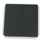
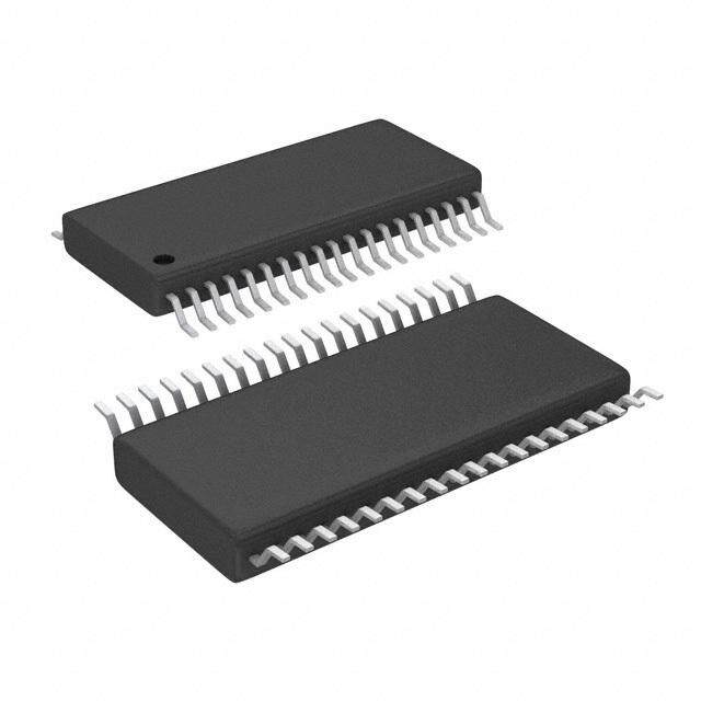
| 供应商器件封装 | 144-LQFP(20x20) |
| 其它名称 | 568-7576 |
| 包装 | 托盘 |
| 可用A/D通道 | 8 |
| 可编程输入/输出端数量 | 141 |
| 商标 | NXP Semiconductors |
| 商标名 | LPC |
| 处理器系列 | ARM Cortex M3 |
| 外设 | 欠压检测/复位,DMA,I²S,电机控制 PWM,POR,PWM,WDT |
| 安装风格 | SMD/SMT |
| 定时器数量 | 4 Timer |
| 封装 | Tray |
| 封装/外壳 | 144-LQFP |
| 封装/箱体 | LQFP-144 |
| 工作温度 | -40°C ~ 85°C |
| 工作电源电压 | 3.3 V |
| 工厂包装数量 | 60 |
| 振荡器类型 | 内部 |
| 接口类型 | Ethernet, RS-232, USB |
| 数据RAM大小 | 96 kB |
| 数据Ram类型 | SRAM |
| 数据ROM大小 | 4 kB |
| 数据Rom类型 | Flash |
| 数据总线宽度 | 32 bit |
| 数据转换器 | A/D 8x12b,D/A 1x10b |
| 最大工作温度 | + 85 C |
| 最大时钟频率 | 50 MHz |
| 最小工作温度 | - 40 C |
| 标准包装 | 60 |
| 核心 | ARM |
| 核心处理器 | ARM® Cortex®-M3 |
| 核心尺寸 | 32-位 |
| 片上ADC | Yes |
| 片上DAC | With DAC |
| 电压-电源(Vcc/Vdd) | 2.4 V ~ 3.6 V |
| 程序存储器大小 | 512 kB |
| 程序存储器类型 | EEPROM |
| 程序存储容量 | 512KB(512K x 8) |
| 输入/输出端数量 | 141 I/O |
| 连接性 | CAN, EBI/EMI, 以太网, I²C, Microwire, 存储器卡, SPI, SSI, SSP, UART/USART, USB OTG |
| 速度 | 120MHz |


- 商务部:美国ITC正式对集成电路等产品启动337调查
- 曝三星4nm工艺存在良率问题 高通将骁龙8 Gen1或转产台积电
- 太阳诱电将投资9.5亿元在常州建新厂生产MLCC 预计2023年完工
- 英特尔发布欧洲新工厂建设计划 深化IDM 2.0 战略
- 台积电先进制程称霸业界 有大客户加持明年业绩稳了
- 达到5530亿美元!SIA预计今年全球半导体销售额将创下新高
- 英特尔拟将自动驾驶子公司Mobileye上市 估值或超500亿美元
- 三星加码芯片和SET,合并消费电子和移动部门,撤换高东真等 CEO
- 三星电子宣布重大人事变动 还合并消费电子和移动部门
- 海关总署:前11个月进口集成电路产品价值2.52万亿元 增长14.8%


PDF Datasheet 数据手册内容提取
LPC178x/7x 32-bit ARM Cortex-M3 microcontroller; up to 512 kB flash and 96 kB SRAM; USB Device/Host/OTG; Ethernet; LCD; EMC Rev. 5.5 — 26 April 2016 Product data sheet 1. General description The LPC178x/7x is an ARM Cortex-M3 based microcontroller for embedded applications requiring a high level of integration and low power dissipation. The ARM Cortex-M3 is a next generation core that offers better performance than the ARM7 at the same clock rate and other system enhancements such as modernized debug features and a higher level of support block integration. The ARM Cortex-M3 CPU incorporates a 3-stage pipeline and has a Harvard architecture with separate local instruction and data buses, as well as a third bus with slightly lower performance for peripherals. The ARM Cortex-M3 CPU also includes an internal prefetch unit that supports speculative branches. The LPC178x/7x adds a specialized flash memory accelerator to accomplish optimal performance when executing code from flash. The LPC178x/7x operates at up to 120MHz CPU frequency. The peripheral complement of the LPC178x/7x includes up to 512 kB of flash program memory, up to 96 kB of SRAM data memory, up to 4032 byte of EEPROM data memory, External Memory Controller (EMC), LCD (LPC178x only), Ethernet, USB Device/Host/OTG, a General Purpose DMA controller, five UARTs, three SSP controllers, three I2C-bus interfaces, a Quadrature Encoder Interface, four general purpose timers, two general purpose PWMs with six outputs each and one motor control PWM, an ultra-low power RTC with separate battery supply and event recorder, a windowed watchdog timer, a CRC calculation engine, up to 165 general purpose I/O pins, and more. The analog peripherals include one eight-channel 12-bit ADC and a 10-bit DAC. The pinout of LPC178x/7x is intended to allow pin function compatibility with the LPC24xx and LPC23xx. For additional documentation, see Section 18 “References”. 2. Features and benefits Functional replacement for the LPC23xx and LPC24xx family devices. System: ARM Cortex-M3 processor, running at frequencies of up to 120 MHz. A Memory Protection Unit (MPU) supporting eight regions is included. ARM Cortex-M3 built-in Nested Vectored Interrupt Controller (NVIC).
LPC178x/7x NXP Semiconductors 32-bit ARM Cortex-M3 microcontroller Multilayer AHB matrix interconnect provides a separate bus for each AHB master. AHB masters include the CPU, USB, Ethernet, and the General Purpose DMA controller. This interconnect provides communication with no arbitration delays unless two masters attempt to access the same slave at the same time. Split APB bus allows for higher throughput with fewer stalls between the CPU and DMA. A single level of write buffering allows the CPU to continue without waiting for completion of APB writes if the APB was not already busy. Cortex-M3 system tick timer, including an external clock input option. Standard JTAG test/debug interface as well as Serial Wire Debug and Serial WireTrace Port options. Embedded Trace Macrocell (ETM) module supports real-time trace. Boundary scan for simplified board testing. Non-maskable Interrupt (NMI) input. Memory: Up to 512 kB on-chip flash program memory with In-System Programming (ISP) and In-Application Programming (IAP) capabilities. The combination of an enhanced flash memory accelerator and location of the flash memory on the CPU local code/data bus provides high code performance from flash. Up to 96 kB on-chip SRAM includes: 64 kB of main SRAM on the CPU with local code/data bus for high-performance CPU access. Two 16 kB peripheral SRAM blocks with separate access paths for higher throughput. These SRAM blocks may be used for DMA memory as well as for general purpose instruction and data storage. Up to 4032 byte on-chip EEPROM. LCD controller, supporting both Super-Twisted Nematic (STN) and Thin-Film Transistors (TFT) displays. Dedicated DMA controller. Selectable display resolution (up to 1024768 pixels). Supports up to 24-bit true-color mode. External Memory Controller (EMC) provides support for asynchronous static memory devices such as RAM, ROM and flash, as well as dynamic memories such as single data rate SDRAM with an SDRAM clock of up to 80 MHz. Eight channel General Purpose DMA controller (GPDMA) on the AHB multilayer matrix that can be used with the SSP, I2S, UART, CRC engine, Analog-to-Digital and Digital-to-Analog converter peripherals, timer match signals, GPIO, and for memory-to-memory transfers. Serial interfaces: Ethernet MAC with MII/RMII interface and associated DMA controller. These functions reside on an independent AHB. USB 2.0 full-speed dual-port device/host/OTG controller with on-chip PHY and associated DMA controller. Five UARTs with fractional baud rate generation, internal FIFO, DMA support, and RS-485/EIA-485 support. One UART (UART1) has full modem control I/O, and one UART (USART4) supports IrDA, synchronous mode, and a smart card mode conforming to ISO7816-3. Three SSP controllers with FIFO and multi-protocol capabilities. The SSP controllers can be used with the GPDMA. LPC178X_7X All information provided in this document is subject to legal disclaimers. © NXP Semiconductors N.V. 2016. All rights reserved. Product data sheet Rev. 5.5 — 26 April 2016 2 of 126
LPC178x/7x NXP Semiconductors 32-bit ARM Cortex-M3 microcontroller Three enhanced I2C-bus interfaces, one with a true open-drain output supporting the full I2C-bus specification and Fast-mode Plus with data rates of 1 Mbit/s, two with standard port pins. Enhancements include multiple address recognition and monitor mode. I2S-bus (Inter-IC Sound) interface for digital audio input or output. It can be used with the GPDMA. CAN controller with two channels. Digital peripherals: SD/MMC memory card interface. Up to 165 General Purpose I/O (GPIO) pins depending on the packaging with configurable pull-up/down resistors, open-drain mode, and repeater mode. All GPIOs are located on an AHB bus for fast access and support Cortex-M3 bit-banding. GPIOs can be accessed by the General Purpose DMA Controller. Any pin of ports 0 and 2 can be used to generate an interrupt. Two external interrupt inputs configurable as edge/level sensitive. All pins on port 0 and port 2 can be used as edge sensitive interrupt sources. Four general purpose timers/counters with a total of eight capture inputs and ten compare outputs. Each timer block has an external count input. Specific timer events can be selected to generate DMA requests. Quadrature encoder interface that can monitor one external quadrature encoder. Two standard PWM/timer blocks with external count input option. One motor control PWM with support for three-phase motor control. Real-Time Clock (RTC) with a separate power domain. The RTC is clocked by a dedicated RTC oscillator. The RTC block includes 20 bytes of battery-powered backup registers, allowing system status to be stored when the rest of the chip is powered off. Battery power can be supplied from a standard 3 V lithium button cell. The RTC will continue working when the battery voltage drops to as low as 2.1 V. An RTC interrupt can wake up the CPU from any reduced power mode. Event Recorder that can capture the clock value when an event occurs on any of three inputs. The event identification and the time it occurred are stored in registers. The Event Recorder is located in the RTC power domain and can therefore operate as long as there is RTC power. Windowed Watchdog Timer (WWDT). Windowed operation, dedicated internal oscillator, watchdog warning interrupt, and safety features. CRC Engine block can calculate a CRC on supplied data using one of three standard polynomials. The CRC engine can be used in conjunction with the DMA controller to generate a CRC without CPU involvement in the data transfer. Analog peripherals: 12-bit Analog-to-Digital Converter (ADC) with input multiplexing among eight pins, conversion rates up to 400 kHz, and multiple result registers. The 12-bit ADC can be used with the GPDMA controller. 10-bit Digital-to-Analog Converter (DAC) with dedicated conversion timer and GPDMA support. Power control: Four reduced power modes: Sleep, Deep-sleep, Power-down, and Deep power-down. LPC178X_7X All information provided in this document is subject to legal disclaimers. © NXP Semiconductors N.V. 2016. All rights reserved. Product data sheet Rev. 5.5 — 26 April 2016 3 of 126
LPC178x/7x NXP Semiconductors 32-bit ARM Cortex-M3 microcontroller The Wake-up Interrupt Controller (WIC) allows the CPU to automatically wake up from any priority interrupt that can occur while the clocks are stopped in Deep-sleep, Power-down, and Deep power-down modes. Processor wake-up from Power-down mode via any interrupt able to operate during Power-down mode (includes external interrupts, RTC interrupt, PORT0/2 pin interrupt, and NMI). Brownout detect with separate threshold for interrupt and forced reset. On-chip Power-On Reset (POR). Clock generation: Clock output function that can reflect the main oscillator clock, IRC clock, RTC clock, CPU clock, USB clock, or the watchdog timer clock. On-chip crystal oscillator with an operating range of 1 MHz to 25 MHz. 12 MHz Internal RC oscillator (IRC) trimmed to 1% accuracy that can optionally be used as a system clock. An on-chip PLL allows CPU operation up to the maximum CPU rate without the need for a high-frequency crystal. May be run from the main oscillator or the internal RC oscillator. A second, dedicated PLL may be used for USB interface in order to allow added flexibility for the Main PLL settings. Versatile pin function selection feature allows many possibilities for using on-chip peripheral functions. Unique device serial number for identification purposes. Single 3.3 V power supply (2.4 V to 3.6 V). Temperature range of 40 C to 85 C. Available as LQFP208, TFBGA208, TFBGA180, and LQFP144 package. 3. Applications Communications: Point-of-sale terminals, web servers, multi-protocol bridges Industrial/Medical: Automation controllers, application control, robotics control, HVAC, PLC, inverters, circuit breakers, medical scanning, security monitoring, motor drive, video intercom Consumer/Appliance: Audio, MP3 decoders, alarm systems, displays, printers, scanners, small appliances, fitness equipment Automotive: After-market, car alarms, GPS/fleet monitors LPC178X_7X All information provided in this document is subject to legal disclaimers. © NXP Semiconductors N.V. 2016. All rights reserved. Product data sheet Rev. 5.5 — 26 April 2016 4 of 126
LPC178x/7x NXP Semiconductors 32-bit ARM Cortex-M3 microcontroller 4. Ordering information Table 1. Ordering info rmation Type number Package Name Description Version LPC1788 LPC1788FBD208 LQFP208 plastic low profile quad flat package; 208 leads; body 28 28 1.4 mm SOT459-1 LPC1788FET208 TFBGA208 plastic thin fine-pitch ball grid array package; 208 balls; body SOT950-1 15 ´ 15 ´ 0.7 mm LPC1788FET180 TFBGA180 thin fine-pitch ball grid array package; 180 balls; body 12 ´ 12 ´ 0.8 mm SOT570-3 LPC1788FBD144 LQFP144 plastic low profile quad flat package; 144 leads; body 20 20 1.4 mm SOT486-1 LPC1787 LPC1787FBD208 LQFP208 plastic low profile quad flat package; 208 leads; body 28 28 1.4 mm SOT459-1 LPC1786 LPC1786FBD208 LQFP208 plastic low profile quad flat package; 208 leads; body 28 28 1.4 mm SOT459-1 LPC1785 LPC1785FBD208 LQFP208 plastic low profile quad flat package; 208 leads; body 28 28 1.4 mm SOT459-1 LPC1778 LPC1778FBD208 LQFP208 plastic low profile quad flat package; 208 leads; body 28 28 1.4 mm SOT459-1 LPC1778FET208 TFBGA208 plastic thin fine-pitch ball grid array package; 208 balls; body SOT950-1 15 ´ 15 ´ 0.7 mm LPC1778FET180 TFBGA180 thin fine-pitch ball grid array package; 180 balls; body 12 ´ 12 ´ 0.8 mm SOT570-3 LPC1778FBD144 LQFP144 plastic low profile quad flat package; 144 leads; body 20 20 1.4 mm SOT486-1 LPC1777 LPC1777FBD208 LQFP208 plastic low profile quad flat package; 208 leads; body 28 28 1.4 mm SOT459-1 LPC1776 LPC1776FBD208 LQFP208 plastic low profile quad flat package; 208 leads; body 28 28 1.4 mm SOT459-1 LPC1776FET180 TFBGA180 thin fine-pitch ball grid array package; 180 balls; body 12 ´ 12 ´ 0.8 mm SOT570-3 LPC1774 LPC1774FBD208 LQFP208 plastic low profile quad flat package; 208 leads; body 28 28 1.4 mm SOT459-1 LPC1774FBD144 LQFP144 plastic low profile quad flat package; 144 leads; body 20 20 1.4 mm SOT486-1 LPC178X_7X All information provided in this document is subject to legal disclaimers. © NXP Semiconductors N.V. 2016. All rights reserved. Product data sheet Rev. 5.5 — 26 April 2016 5 of 126
LPC178x/7x NXP Semiconductors 32-bit ARM Cortex-M3 microcontroller Table 2. LPC178x/7x ordering options All parts include two CAN channels, three SSP interfaces, three I2C interfaces, one I2S interface, DAC, and an 8-channel 12-bit ADC. Type number Device order part number Flash(kB) Main SRAM(kB) Peripheral SRAM (kB) Total SRAM (kB) EEPROM(byte) Ethernet USB UART EMC bus [1]width (bit) GPIO LCD QEI SD/MMC LPC178x LPC1788FBD208 LPC1788FBD208/CP3E 512 64 16 2 96 4032 Y H/O/D 5 32 165 Y Y Y LPC1788FET208 LPC1788FET208,551 512 64 16 2 96 4032 Y H/O/D 5 32 165 Y Y Y LPC1788FET180 LPC1788FET180,551 512 64 16 2 96 4032 Y H/O/D 5 16 141 Y Y Y LPC1788FBD144 LPC1788FBD144,551 512 64 16 2 96 4032 Y H/O/D 5 8 109 Y Y Y LPC1787FBD208 LPC1787FBD208,551 512 64 16 2 96 4032 N H/O/D 5 32 165 Y Y Y LPC1786FBD208 LPC1786FBD208,551 256 64 16 80 4032 Y H/O/D 5 32 165 Y Y Y LPC1785FBD208 LPC1785FBD208K 256 64 16 80 4032 N H/O/D 5 32 165 Y N Y LPC177x LPC1778FBD208 LPC1778FBD208,551 512 64 16 2 96 4032 Y H/O/D 5 32 165 N Y Y LPC1778FET208 LPC1778FET208,551 512 64 16 2 96 4032 Y H/O/D 5 32 165 N Y Y LPC1778FET180 LPC1778FET180,551 512 64 16 2 96 4032 Y H/O/D 5 16 141 N Y Y LPC1778FBD144 LPC1778FBD144,551 512 64 16 2 96 4032 Y H/O/D 5 8 109 N Y Y LPC1777FBD208 LPC1777FBD208,551 512 64 16 2 96 4032 N H/O/D 5 32 165 N Y Y LPC1776FBD208 LPC1776FBD208,551 256 64 16 80 4032 Y H/O/D 5 32 165 N Y Y LPC1776FET180 LPC1776FET180,551 256 64 16 80 4032 Y H/O/D 5 16 141 N Y Y LPC1774FBD208 LPC1774FBD208,551 128 32 8 40 2048 N D 5 32 165 N N N LPC1774FBD144 LPC1774FBD144,551 128 32 8 40 2048 N D 4[2] 8 109 N N N [1] Maximum data bus width of the External Memory Controller (EMC) depends on package size. Smaller widths may be used. [2] USART4 not available. LPC178X_7X All information provided in this document is subject to legal disclaimers. © NXP Semiconductors N.V. 2016. All rights reserved. Product data sheet Rev. 5.5 — 26 April 2016 6 of 126
LPC178x/7x NXP Semiconductors 32-bit ARM Cortex-M3 microcontroller 5. Block diagram debug JTAG port interface LPC178x/7x ONDULE TIENSTTE/RDFEABCUEG GENCELROACTKION, ATIMO POWER CONTROL, EMULRACE CORATREMX-M3 MPU CONGTPRDOMLALER ETHERNET(1) HOSDTEU(V1S)I/CBOET/G(1) FUSNYCSTTEIOMN S T clocks and I-code D-code system master master master controls bus bus bus slave slave EMC ROM slave slave LCD(1) MULTILAYER AHB MATRIX SRAM 96/80/40 kB slave slave slave slave slave HIGH-SPEED GPIO CRC AHB TO AHB TO FLASH 4032 B/ APB APB ACCELERATOR 2048 B APB slave group 0 BRIDGE 0 BRIDGE 1 FLASH EEPROM 512/256/128/64 kB SSP1 APB slave group 1 SSP0/2 UART0/1 UART2/3 I2C0/1 USART4(1) CAN 0/1 I2C2 TIMER 0/1 SD/MMC(1) WINDOWED WDT TIMER2/3 PWM0/1 QUADRATURE ENCODER(1) 12-bit ADC DAC PIN CONNECT I2S GPIO INTERRUPT CONTROL MOTOR CONTROL PWM EVENT RECORDER 32 kHz SYSTEM CONTROL RTC OSCILLATOR BACKUP REGISTERS = connected to GPDMA RTC POWER DOMAIN 002aaf528 (1) Not available on all parts. See Table2. Fig 1. Block diagram LPC178X_7X All information provided in this document is subject to legal disclaimers. © NXP Semiconductors N.V. 2016. All rights reserved. Product data sheet Rev. 5.5 — 26 April 2016 7 of 126
LPC178x/7x NXP Semiconductors 32-bit ARM Cortex-M3 microcontroller 6. Pinning information 6.1 Pinning 8 7 0 5 2 1 1 156 LPC178x/7xFBD208 52 105 3 4 5 10 002aaf518 Fig 2. Pin configuration (LQFP208) ball A1 index area 2 4 6 8 10 12 14 16 1 3 5 7 9 11 13 15 17 A B C D E F G H J LPC178x/7x K L M N P R T U 002aaf529 Transparent top view Fig 3. Pin configuration (TFBGA208) LPC178X_7X All information provided in this document is subject to legal disclaimers. © NXP Semiconductors N.V. 2016. All rights reserved. Product data sheet Rev. 5.5 — 26 April 2016 8 of 126
LPC178x/7x NXP Semiconductors 32-bit ARM Cortex-M3 microcontroller ball A1 LPC178x/7x index area 1 2 3 4 5 6 7 8 9 1011121314 A B C D E F G H J K L M N P 002aaf519 Transparent top view Fig 4. Pin configuration (TFBGA180) 4 9 4 0 1 1 1 108 LPC178x/7x 36 73 7 2 3 7 002aaf520 Fig 5. Pin configuration (LQFP144) 6.2 Pin description I/O pins on the LPC178x/7x are 5V tolerant and have input hysteresis unless otherwise indicated in the table below. Crystal pins, power pins, and reference voltage pins are not 5V tolerant. In addition, when pins are selected to be ADC inputs, they are no longer 5V tolerant and the input voltage must be limited to the voltage at the ADC positive reference pin (VREFP). All port pins Pn[m] are multiplexed, and the multiplexed functions appear in Table3 in the order defined by the FUNC bits of the corresponding IOCON register up to the highest used function number. Each port pin can support up to eight multiplexed functions. IOCON register FUNC values which are reserved are noted as ‘R’ in the pin configuration table. LPC178X_7X All information provided in this document is subject to legal disclaimers. © NXP Semiconductors N.V. 2016. All rights reserved. Product data sheet Rev. 5.5 — 26 April 2016 9 of 126
LPC178x/7x NXP Semiconductors 32-bit ARM Cortex-M3 microcontroller Table 3. Pin descripti on Not all functions are available on all parts. See Table2 (Ethernet, USB, LCD, QEI, SD/MMC, DAC pins) and Table7 (EMC pins). Symbol 8 0 Description 0 8 8 2 1 4 1] P20 GA GA P14 [ate Pin LQF Ball TFB Ball TFB Pin LQF Reset st [2]Type P0[0] to I/O Port 0: Port 0 is a 32-bit I/O port with individual direction P0[31] controls for each bit. The operation of port 0 pins depends upon the pin function selected via the pin connect block. P0[0] 94 U15 M10 66 [3] I; I/O P0[0] — General purpose digital input/output pin. PU I CAN_RD1 — CAN1 receiver input. O U3_TXD — Transmitter output for UART3. I/O I2C1_SDA — I2C1 data input/output (this pin does not use a specialized I2C pad). O U0_TXD — Transmitter output for UART0. P0[1] 96 T14 N11 67 [3] I; I/O P0[1] — General purpose digital input/output pin. PU O CAN_TD1 — CAN1 transmitter output. I U3_RXD — Receiver input for UART3. I/O I2C1_SCL — I2C1 clock input/output (this pin does not use a specialized I2C pad). I U0_RXD — Receiver input for UART0. P0[2] 202 C4 D5 141 [3] I; I/O P0[2] — General purpose digital input/output pin. PU O U0_TXD — Transmitter output for UART0. O U3_TXD — Transmitter output for UART3. P0[3] 204 D6 A3 142 [3] I; I/O P0[3] — General purpose digital input/output pin. PU I U0_RXD — Receiver input for UART0. I U3_RXD — Receiver input for UART3. P0[4] 168 B12 A11 116 [3] I; I/O P0[4] — General purpose digital input/output pin. PU I/O I2S_RX_SCK — I2S Receive clock. It is driven by the master and received by the slave. Corresponds to the signal SCK in the I2S-bus specification. I CAN_RD2 — CAN2 receiver input. I T2_CAP0 — Capture input for Timer2, channel 0. - R — Function reserved. - R — Function reserved. - R — Function reserved. O LCD_VD[0] — LCD data. LPC178X_7X All information provided in this document is subject to legal disclaimers. © NXP Semiconductors N.V. 2016. All rights reserved. Product data sheet Rev. 5.5 — 26 April 2016 10 of 126
LPC178x/7x NXP Semiconductors 32-bit ARM Cortex-M3 microcontroller Table 3. Pin description …continued Not all functions are available on all parts. See Table2 (Ethernet, USB, LCD, QEI, SD/MMC, DAC pins) and Table7 (EMC pins). Symbol 8 0 Description 0 8 8 2 1 4 1] P20 GA GA P14 [ate Pin LQF Ball TFB Ball TFB Pin LQF Reset st [2]Type P0[5] 166 C12 B11 115 [3] I; I/O P0[5] — General purpose digital input/output pin. PU I/O I2S_RX_WS — I2S Receive word select. It is driven by the master and received by the slave. Corresponds to the signal WS in the I2S-bus specification. O CAN_TD2 — CAN2 transmitter output. I T2_CAP1 — Capture input for Timer2, channel 1. - R — Function reserved. - R — Function reserved. - R — Function reserved. O LCD_VD[1] — LCD data. P0[6] 164 D13 D11 113 [3] I; I/O P0[6] — General purpose digital input/output pin. PU I/O I2S_RX_SDA — I2S Receive data. It is driven by the transmitter and read by the receiver. Corresponds to the signal SD in the I2S-bus specification. I/O SSP1_SSEL — Slave Select for SSP1. O T2_MAT0 — Match output for Timer2, channel 0. O U1_RTS — Request to Send output for UART1. Can also be configured to be an RS-485/EIA-485 output enable signal for UART1. - R — Function reserved. - R — Function reserved. O LCD_VD[8] — LCD data. P0[7] 162 C13 B12 112 [4] I; IA I/O P0[7] — General purpose digital input/output pin. I/O I2S_TX_SCK — I2S transmit clock. It is driven by the master and received by the slave. Corresponds to the signal SCK in the I2S-bus specification. I/O SSP1_SCK — Serial Clock for SSP1. O T2_MAT1 — Match output for Timer2, channel 1. I RTC_EV0 — Event input 0 to Event Monitor/Recorder. - R — Function reserved. - R — Function reserved. O LCD_VD[9] — LCD data. LPC178X_7X All information provided in this document is subject to legal disclaimers. © NXP Semiconductors N.V. 2016. All rights reserved. Product data sheet Rev. 5.5 — 26 April 2016 11 of 126
LPC178x/7x NXP Semiconductors 32-bit ARM Cortex-M3 microcontroller Table 3. Pin description …continued Not all functions are available on all parts. See Table2 (Ethernet, USB, LCD, QEI, SD/MMC, DAC pins) and Table7 (EMC pins). Symbol 8 0 Description 0 8 8 2 1 4 1] P20 GA GA P14 [ate Pin LQF Ball TFB Ball TFB Pin LQF Reset st [2]Type P0[8] 160 A15 C12 111 [4] I; IA I/O P0[8] — General purpose digital input/output pin. I/O I2S_TX_WS — I2S Transmit word select. It is driven by the master and received by the slave. Corresponds to the signal WS in the I2S-bus specification. I/O SSP1_MISO — Master In Slave Out for SSP1. O T2_MAT2 — Match output for Timer2, channel 2. I RTC_EV1 — Event input 1 to Event Monitor/Recorder. - R — Function reserved. - R — Function reserved. O LCD_VD[16] — LCD data. P0[9] 158 C14 A13 109 [4] I; IA I/O P0[9] — General purpose digital input/output pin. I/O I2S_TX_SDA — I2S transmit data. It is driven by the transmitter and read by the receiver. Corresponds to the signal SD in the I2S-bus specification. I/O SSP1_MOSI — Master Out Slave In for SSP1. O T2_MAT3 — Match output for Timer2, channel 3. I RTC_EV2 — Event input 2 to Event Monitor/Recorder. - R — Function reserved. - R — Function reserved. O LCD_VD[17] — LCD data. P0[10] 98 T15 L10 69 [3] I; I/O P0[10] — General purpose digital input/output pin. PU O U2_TXD — Transmitter output for UART2. I/O I2C2_SDA — I2C2 data input/output (this pin does not use a specialized I2C pad). O T3_MAT0 — Match output for Timer3, channel 0. P0[11] 100 R14 P12 70 [3] I; I/O P0[11] — General purpose digital input/output pin. PU I U2_RXD — Receiver input for UART2. I/O I2C2_SCL — I2C2 clock input/output (this pin does not use a specialized I2C pad). O T3_MAT1 — Match output for Timer3, channel 1. P0[12] 41 R1 J4 29 [5] I; I/O P0[12] — General purpose digital input/output pin. PU O USB_PPWR2 — Port Power enable signal for USB port 2. I/O SSP1_MISO — Master In Slave Out for SSP1. I ADC0_IN[6] — A/D converter 0, input 6. When configured as an ADC input, the digital function of the pin must be disabled. LPC178X_7X All information provided in this document is subject to legal disclaimers. © NXP Semiconductors N.V. 2016. All rights reserved. Product data sheet Rev. 5.5 — 26 April 2016 12 of 126
LPC178x/7x NXP Semiconductors 32-bit ARM Cortex-M3 microcontroller Table 3. Pin description …continued Not all functions are available on all parts. See Table2 (Ethernet, USB, LCD, QEI, SD/MMC, DAC pins) and Table7 (EMC pins). Symbol 8 0 Description 0 8 8 2 1 4 1] P20 GA GA P14 [ate Pin LQF Ball TFB Ball TFB Pin LQF Reset st [2]Type P0[13] 45 R2 J5 32 [5] I; I/O P0[13] — General purpose digital input/output pin. PU O USB_UP_LED2 — USB port 2 GoodLink LED indicator. It is LOW when the device is configured (non-control endpoints enabled), or when the host is enabled and has detected a device on the bus. It is HIGH when the device is not configured, or when host is enabled and has not detected a device on the bus, or during global suspend. It transitions between LOW and HIGH (flashes) when the host is enabled and detects activity on the bus. I/O SSP1_MOSI — Master Out Slave In for SSP1. I ADC0_IN[7] — A/D converter 0, input 7. When configured as an ADC input, the digital function of the pin must be disabled. P0[14] 69 T7 M5 48 [3] I; I/O P0[14] — General purpose digital input/output pin. PU O USB_HSTEN2 — Host Enabled status for USB port 2. I/O SSP1_SSEL — Slave Select for SSP1. O USB_CONNECT2 — SoftConnect control for USB port 2. Signal used to switch an external 1.5k resistor under software control. Used with the SoftConnect USB feature. P0[15] 128 J16 H13 89 [3] I; I/O P0[15] — General purpose digital input/output pin. PU O U1_TXD — Transmitter output for UART1. I/O SSP0_SCK — Serial clock for SSP0. P0[16] 130 J14 H14 90 [3] I; I/O P0[16] — General purpose digital input/output pin. PU I U1_RXD — Receiver input for UART1. I/O SSP0_SSEL — Slave Select for SSP0. P0[17] 126 K17 J12 87 [3] I; I/O P0[17] — General purpose digital input/output pin. PU I U1_CTS — Clear to Send input for UART1. I/O SSP0_MISO — Master In Slave Out for SSP0. P0[18] 124 K15 J13 86 [3] I; I/O P0[18] — General purpose digital input/output pin. PU I U1_DCD — Data Carrier Detect input for UART1. I/O SSP0_MOSI — Master Out Slave In for SSP0. P0[19] 122 L17 J10 85 [3] I; I/O P0[19] — General purpose digital input/output pin. PU I U1_DSR — Data Set Ready input for UART1. O SD_CLK — Clock output line for SD card interface. I/O I2C1_SDA — I2C1 data input/output (this pin does not use a specialized I2C pad). LPC178X_7X All information provided in this document is subject to legal disclaimers. © NXP Semiconductors N.V. 2016. All rights reserved. Product data sheet Rev. 5.5 — 26 April 2016 13 of 126
LPC178x/7x NXP Semiconductors 32-bit ARM Cortex-M3 microcontroller Table 3. Pin description …continued Not all functions are available on all parts. See Table2 (Ethernet, USB, LCD, QEI, SD/MMC, DAC pins) and Table7 (EMC pins). Symbol 8 0 Description 0 8 8 2 1 4 1] P20 GA GA P14 [ate Pin LQF Ball TFB Ball TFB Pin LQF Reset st [2]Type P0[20] 120 M17 K14 83 [3] I; I/O P0[20] — General purpose digital input/output pin. PU O U1_DTR — Data Terminal Ready output for UART1. Can also be configured to be an RS-485/EIA-485 output enable signal for UART1. I/O SD_CMD — Command line for SD card interface. I/O I2C1_SCL — I2C1 clock input/output (this pin does not use a specialized I2C pad). P0[21] 118 M16 K11 82 [3] I; I/O P0[21] — General purpose digital input/output pin. PU I U1_RI — Ring Indicator input for UART1. O SD_PWR — Power Supply Enable for external SD card power supply. O U4_OE — RS-485/EIA-485 output enable signal for UART4. I CAN_RD1 — CAN1 receiver input. I/O U4_SCLK — USART 4 clock input or output in synchronous mode. P0[22] 116 N17 L14 80 [6] I; I/O P0[22] — General purpose digital input/output pin. PU O U1_RTS — Request to Send output for UART1. Can also be configured to be an RS-485/EIA-485 output enable signal for UART1. I/O SD_DAT[0] — Data line 0 for SD card interface. O U4_TXD — Transmitter output for USART4 (input/output in smart card mode). O CAN_TD1 — CAN1 transmitter output. P0[23] 18 H1 F5 13 [5] I; I/O P0[23] — General purpose digital input/output pin. PU I ADC0_IN[0] — A/D converter 0, input 0. When configured as an ADC input, the digital function of the pin must be disabled. I/O I2S_RX_SCK — Receive Clock. It is driven by the master and received by the slave. Corresponds to the signal SCK in the I2S-bus specification. I T3_CAP0 — Capture input for Timer3, channel 0. P0[24] 16 G2 E1 11 [5] I; I/O P0[24] — General purpose digital input/output pin. PU I ADC0_IN[1] — A/D converter 0, input 1. When configured as an ADC input, the digital function of the pin must be disabled. I/O I2S_RX_WS — Receive Word Select. It is driven by the master and received by the slave. Corresponds to the signal WS in the I2S-bus specification. I T3_CAP1 — Capture input for Timer3, channel 1. LPC178X_7X All information provided in this document is subject to legal disclaimers. © NXP Semiconductors N.V. 2016. All rights reserved. Product data sheet Rev. 5.5 — 26 April 2016 14 of 126
LPC178x/7x NXP Semiconductors 32-bit ARM Cortex-M3 microcontroller Table 3. Pin description …continued Not all functions are available on all parts. See Table2 (Ethernet, USB, LCD, QEI, SD/MMC, DAC pins) and Table7 (EMC pins). Symbol 8 0 Description 0 8 8 2 1 4 1] P20 GA GA P14 [ate Pin LQF Ball TFB Ball TFB Pin LQF Reset st [2]Type P0[25] 14 F1 E4 10 [5] I; I/O P0[25] — General purpose digital input/output pin. PU I ADC0_IN[2] — A/D converter 0, input 2. When configured as an ADC input, the digital function of the pin must be disabled. I/O I2S_RX_SDA — Receive data. It is driven by the transmitter and read by the receiver. Corresponds to the signal SD in the I2S-bus specification. O U3_TXD — Transmitter output for UART3. P0[26] 12 E1 D1 8 [7] I; I/O P0[26] — General purpose digital input/output pin. PU I ADC0_IN[3] — A/D converter 0, input 3. When configured as an ADC input, the digital function of the pin must be disabled. O DAC_OUT — D/A converter output. When configured as the DAC output, the digital function of the pin must be disabled. I U3_RXD — Receiver input for UART3. P0[27] 50 T1 L3 35 [8] I I/O P0[27] — General purpose digital input/output pin. I/O I2C0_SDA — I2C0 data input/output (this pin uses a specialized I2C pad). I/O USB_SDA1 — I2C serial data for communication with an external USB transceiver. P0[28] 48 R3 M1 34 [8] I I/O P0[28] — General purpose digital input/output pin. I/O I2C0_SCL — I2C0 clock input/output (this pin uses a specialized I2C pad). I/O USB_SCL1 — I2C serial clock for communication with an external USB transceiver. P0[29] 61 U4 K5 42 [9] I I/O P0[29] — General purpose digital input/output pin. I/O USB_D+1 — USB port 1 bidirectional D+ line. I EINT0 — External interrupt 0 input. P0[30] 62 R6 N4 43 [9] I I/O P0[30] — General purpose digital input/output pin. I/O USB_D1 — USB port 1 bidirectional D line. I EINT1 — External interrupt 1 input. P0[31] 51 T2 N1 36 [9] I I/O P0[31] — General purpose digital input/output pin. I/O USB_D+2 — USB port 2 bidirectional D+ line. P1[0] to I/O Port 1: Port 1 is a 32bit I/O port with individual direction P1[31] controls for each bit. The operation of port 1 pins depends upon the pin function selected via the pin connect block P1[0] 196 A3 B5 136 [3] I; I/O P1[0] — General purpose digital input/output pin. PU O ENET_TXD0 — Ethernet transmit data 0 (RMII/MII interface). - R — Function reserved. I T3_CAP1 — Capture input for Timer3, channel 1. I/O SSP2_SCK — Serial clock for SSP2. LPC178X_7X All information provided in this document is subject to legal disclaimers. © NXP Semiconductors N.V. 2016. All rights reserved. Product data sheet Rev. 5.5 — 26 April 2016 15 of 126
LPC178x/7x NXP Semiconductors 32-bit ARM Cortex-M3 microcontroller Table 3. Pin description …continued Not all functions are available on all parts. See Table2 (Ethernet, USB, LCD, QEI, SD/MMC, DAC pins) and Table7 (EMC pins). Symbol 8 0 Description 0 8 8 2 1 4 1] P20 GA GA P14 [ate Pin LQF Ball TFB Ball TFB Pin LQF Reset st [2]Type P1[1] 194 B5 A5 135 [3] I; I/O P1[1] — General purpose digital input/output pin. PU O ENET_TXD1 — Ethernet transmit data 1 (RMII/MII interface). - R — Function reserved. O T3_MAT3 — Match output for Timer3, channel 3. I/O SSP2_MOSI — Master Out Slave In for SSP2. P1[2] 185 D9 B7 - [3] I; I/O P1[2] — General purpose digital input/output pin. PU O ENET_TXD2 — Ethernet transmit data 2 (MII interface). O SD_CLK — Clock output line for SD card interface. O PWM0[1] — Pulse Width Modulator 0, output 1. P1[3] 177 A10 A9 - [3] I; I/O P1[3] — General purpose digital input/output pin. PU O ENET_TXD3 — Ethernet transmit data 3 (MII interface). I/O SD_CMD — Command line for SD card interface. O PWM0[2] — Pulse Width Modulator 0, output 2. P1[4] 192 A5 C6 133 [3] I; I/O P1[4] — General purpose digital input/output pin. PU O ENET_TX_EN — Ethernet transmit data enable (RMII/MII interface). - R — Function reserved. O T3_MAT2 — Match output for Timer3, channel 2. I/O SSP2_MISO — Master In Slave Out for SSP2. P1[5] 156 A17 B13 - [3] I; I/O P1[5] — General purpose digital input/output pin. PU O ENET_TX_ER — Ethernet Transmit Error (MII interface). O SD_PWR — Power Supply Enable for external SD card power supply. O PWM0[3] — Pulse Width Modulator 0, output 3. P1[6] 171 B11 B10 - [3] I; I/O P1[6] — General purpose digital input/output pin. PU I ENET_TX_CLK — Ethernet Transmit Clock (MII interface). I/O SD_DAT[0] — Data line 0 for SD card interface. O PWM0[4] — Pulse Width Modulator 0, output 4. P1[7] 153 D14 C13 - [3] I; I/O P1[7] — General purpose digital input/output pin. PU I ENET_COL — Ethernet Collision detect (MII interface). I/O SD_DAT[1] — Data line 1 for SD card interface. O PWM0[5] — Pulse Width Modulator 0, output 5. LPC178X_7X All information provided in this document is subject to legal disclaimers. © NXP Semiconductors N.V. 2016. All rights reserved. Product data sheet Rev. 5.5 — 26 April 2016 16 of 126
LPC178x/7x NXP Semiconductors 32-bit ARM Cortex-M3 microcontroller Table 3. Pin description …continued Not all functions are available on all parts. See Table2 (Ethernet, USB, LCD, QEI, SD/MMC, DAC pins) and Table7 (EMC pins). Symbol 8 0 Description 0 8 8 2 1 4 1] P20 GA GA P14 [ate Pin LQF Ball TFB Ball TFB Pin LQF Reset st [2]Type P1[8] 190 C7 B6 132 [3] I; I/O P1[8] — General purpose digital input/output pin. PU I ENET_CRS (ENET_CRS_DV) — Ethernet Carrier Sense (MII interface) or Ethernet Carrier Sense/Data Valid (RMII interface). - R — Function reserved. O T3_MAT1 — Match output for Timer3, channel 1. I/O SSP2_SSEL — Slave Select for SSP2. P1[9] 188 A6 D7 131 [3] I; I/O P1[9] — General purpose digital input/output pin. PU I ENET_RXD0 — Ethernet receive data 0 (RMII/MII interface). - R — Function reserved. O T3_MAT0 — Match output for Timer3, channel 0. P1[10] 186 C8 A7 129 [3] I; I/O P1[10] — General purpose digital input/output pin. PU I ENET_RXD1 — Ethernet receive data 1 (RMII/MII interface). - R — Function reserved. I T3_CAP0 — Capture input for Timer3, channel 0. P1[11] 163 A14 A12 - [3] I; I/O P1[11] — General purpose digital input/output pin. PU I ENET_RXD2 — Ethernet Receive Data 2 (MII interface). I/O SD_DAT[2] — Data line 2 for SD card interface. O PWM0[6] — Pulse Width Modulator 0, output 6. P1[12] 157 A16 A14 - [3] I; I/O P1[12] — General purpose digital input/output pin. PU I ENET_RXD3 — Ethernet Receive Data (MII interface). I/O SD_DAT[3] — Data line 3 for SD card interface. I PWM0_CAP0 — Capture input for PWM0, channel 0. P1[13] 147 D16 D14 - [3] I; I/O P1[13] — General purpose digital input/output pin. PU I ENET_RX_DV — Ethernet Receive Data Valid (MII interface). P1[14] 184 A7 D8 128 [3] I; I/O P1[14] — General purpose digital input/output pin. PU I ENET_RX_ER — Ethernet receive error (RMII/MII interface). - R — Function reserved. I T2_CAP0 — Capture input for Timer2, channel 0. P1[15] 182 A8 A8 126 [3] I; I/O P1[15] — General purpose digital input/output pin. PU I ENET_RX_CLK (ENET_REF_CLK) — Ethernet Receive Clock (MII interface) or Ethernet Reference Clock (RMII interface). - R — Function reserved. I/O I2C2_SDA — I2C2 data input/output (this pin does not use a specialized I2C pad). LPC178X_7X All information provided in this document is subject to legal disclaimers. © NXP Semiconductors N.V. 2016. All rights reserved. Product data sheet Rev. 5.5 — 26 April 2016 17 of 126
LPC178x/7x NXP Semiconductors 32-bit ARM Cortex-M3 microcontroller Table 3. Pin description …continued Not all functions are available on all parts. See Table2 (Ethernet, USB, LCD, QEI, SD/MMC, DAC pins) and Table7 (EMC pins). Symbol 8 0 Description 0 8 8 2 1 4 1] P20 GA GA P14 [ate Pin LQF Ball TFB Ball TFB Pin LQF Reset st [2]Type P1[16] 180 D10 B8 125 [3] I; I/O P1[16] — General purpose digital input/output pin. PU O ENET_MDC — Ethernet MIIM clock. O I2S_TX_MCLK — I2S transmit master clock. P1[17] 178 A9 C9 123 [3] I; I/O P1[17] — General purpose digital input/output pin. PU I/O ENET_MDIO — Ethernet MIIM data input and output. O I2S_RX_MCLK — I2S receive master clock. P1[18] 66 P7 L5 46 [3] I; I/O P1[18] — General purpose digital input/output pin. PU O USB_UP_LED1 — It is LOW when the device is configured (non-control endpoints enabled), or when the host is enabled and has detected a device on the bus. It is HIGH when the device is not configured, or when host is enabled and has not detected a device on the bus, or during global suspend. It transitions between LOW and HIGH (flashes) when the host is enabled and detects activity on the bus. O PWM1[1] — Pulse Width Modulator 1, channel 1 output. I T1_CAP0 — Capture input for Timer1, channel 0. - R — Function reserved. I/O SSP1_MISO — Master In Slave Out for SSP1. P1[19] 68 U6 P5 47 [3] I; I/O P1[19] — General purpose digital input/output pin. PU O USB_TX_E1 — Transmit Enable signal for USB port 1 (OTG transceiver). O USB_PPWR1 — Port Power enable signal for USB port 1. I T1_CAP1 — Capture input for Timer1, channel 1. O MC_0A — Motor control PWM channel 0, output A. I/O SSP1_SCK — Serial clock for SSP1. O U2_OE — RS-485/EIA-485 output enable signal for UART2. P1[20] 70 U7 K6 49 [3] I; I/O P1[20] — General purpose digital input/output pin. PU O USB_TX_DP1 — D+ transmit data for USB port 1 (OTG transceiver). O PWM1[2] — Pulse Width Modulator 1, channel 2 output. I QEI_PHA — Quadrature Encoder Interface PHA input. I MC_FB0 — Motor control PWM channel 0 feedback input. I/O SSP0_SCK — Serial clock for SSP0. O LCD_VD[6] — LCD data. O LCD_VD[10] — LCD data. LPC178X_7X All information provided in this document is subject to legal disclaimers. © NXP Semiconductors N.V. 2016. All rights reserved. Product data sheet Rev. 5.5 — 26 April 2016 18 of 126
LPC178x/7x NXP Semiconductors 32-bit ARM Cortex-M3 microcontroller Table 3. Pin description …continued Not all functions are available on all parts. See Table2 (Ethernet, USB, LCD, QEI, SD/MMC, DAC pins) and Table7 (EMC pins). Symbol 8 0 Description 0 8 8 2 1 4 1] P20 GA GA P14 [ate Pin LQF Ball TFB Ball TFB Pin LQF Reset st [2]Type P1[21] 72 R8 N6 50 [3] I; I/O P1[21] — General purpose digital input/output pin. PU O USB_TX_DM1 — D transmit data for USB port 1 (OTG transceiver). O PWM1[3] — Pulse Width Modulator 1, channel 3 output. I/O SSP0_SSEL — Slave Select for SSP0. I MC_ABORT — Motor control PWM, active low fast abort. - R — Function reserved. O LCD_VD[7] — LCD data. O LCD_VD[11] — LCD data. P1[22] 74 U8 M6 51 [3] I; I/O P1[22] — General purpose digital input/output pin. PU I USB_RCV1 — Differential receive data for USB port 1 (OTG transceiver). I USB_PWRD1 — Power Status for USB port 1 (host power switch). O T1_MAT0 — Match output for Timer1, channel 0. O MC_0B — Motor control PWM channel 0, output B. I/O SSP1_MOSI — Master Out Slave In for SSP1. O LCD_VD[8] — LCD data. O LCD_VD[12] — LCD data. P1[23] 76 P9 N7 53 [3] I; I/O P1[23] — General purpose digital input/output pin. PU I USB_RX_DP1 — D+ receive data for USB port 1 (OTG transceiver). O PWM1[4] — Pulse Width Modulator 1, channel 4 output. I QEI_PHB — Quadrature Encoder Interface PHB input. I MC_FB1 — Motor control PWM channel 1 feedback input. I/O SSP0_MISO — Master In Slave Out for SSP0. O LCD_VD[9] — LCD data. O LCD_VD[13] — LCD data. P1[24] 78 T9 P7 54 [3] I; I/O P1[24] — General purpose digital input/output pin. PU I USB_RX_DM1 — D receive data for USB port 1 (OTG transceiver). O PWM1[5] — Pulse Width Modulator 1, channel 5 output. I QEI_IDX — Quadrature Encoder Interface INDEX input. I MC_FB2 — Motor control PWM channel 2 feedback input. I/O SSP0_MOSI — Master Out Slave in for SSP0. O LCD_VD[10] — LCD data. O LCD_VD[14] — LCD data. LPC178X_7X All information provided in this document is subject to legal disclaimers. © NXP Semiconductors N.V. 2016. All rights reserved. Product data sheet Rev. 5.5 — 26 April 2016 19 of 126
LPC178x/7x NXP Semiconductors 32-bit ARM Cortex-M3 microcontroller Table 3. Pin description …continued Not all functions are available on all parts. See Table2 (Ethernet, USB, LCD, QEI, SD/MMC, DAC pins) and Table7 (EMC pins). Symbol 8 0 Description 0 8 8 2 1 4 1] P20 GA GA P14 [ate Pin LQF Ball TFB Ball TFB Pin LQF Reset st [2]Type P1[25] 80 T10 L7 56 [3] I; I/O P1[25] — General purpose digital input/output pin. PU O USB_LS1 — Low Speed status for USB port 1 (OTG transceiver). O USB_HSTEN1 — Host Enabled status for USB port 1. O T1_MAT1 — Match output for Timer1, channel 1. O MC_1A — Motor control PWM channel 1, output A. O CLKOUT — Selectable clock output. O LCD_VD[11] — LCD data. O LCD_VD[15] — LCD data. P1[26] 82 R10 P8 57 [3] I; I/O P1[26] — General purpose digital input/output pin. PU O USB_SSPND1 — USB port 1 Bus Suspend status (OTG transceiver). O PWM1[6] — Pulse Width Modulator 1, channel 6 output. I T0_CAP0 — Capture input for Timer0, channel 0. O MC_1B — Motor control PWM channel 1, output B. I/O SSP1_SSEL — Slave Select for SSP1. O LCD_VD[12] — LCD data. O LCD_VD[20] — LCD data. P1[27] 88 T12 M9 61 [3] I; I/O P1[27] — General purpose digital input/output pin. PU I USB_INT1 — USB port 1 OTG transceiver interrupt (OTG transceiver). I USB_OVRCR1 — USB port 1 Over-Current status. I T0_CAP1 — Capture input for Timer0, channel 1. O CLKOUT — Selectable clock output. - R — Function reserved. O LCD_VD[13] — LCD data. O LCD_VD[21] — LCD data. P1[28] 90 T13 P10 63 [3] I; I/O P1[28] — General purpose digital input/output pin. PU I/O USB_SCL1 — USB port 1 I2C serial clock (OTG transceiver). I PWM1_CAP0 — Capture input for PWM1, channel 0. O T0_MAT0 — Match output for Timer0, channel 0. O MC_2A — Motor control PWM channel 2, output A. I/O SSP0_SSEL — Slave Select for SSP0. O LCD_VD[14] — LCD data. O LCD_VD[22] — LCD data. LPC178X_7X All information provided in this document is subject to legal disclaimers. © NXP Semiconductors N.V. 2016. All rights reserved. Product data sheet Rev. 5.5 — 26 April 2016 20 of 126
LPC178x/7x NXP Semiconductors 32-bit ARM Cortex-M3 microcontroller Table 3. Pin description …continued Not all functions are available on all parts. See Table2 (Ethernet, USB, LCD, QEI, SD/MMC, DAC pins) and Table7 (EMC pins). Symbol 8 0 Description 0 8 8 2 1 4 1] P20 GA GA P14 [ate Pin LQF Ball TFB Ball TFB Pin LQF Reset st [2]Type P1[29] 92 U14 N10 64 [3] I; I/O P1[29] — General purpose digital input/output pin. PU I/O USB_SDA1 — USB port 1 I2C serial data (OTG transceiver). I PWM1_CAP1 — Capture input for PWM1, channel 1. O T0_MAT1 — Match output for Timer0, channel 1. O MC_2B — Motor control PWM channel 2, output B. O U4_TXD — Transmitter output for USART4 (input/output in smart card mode). O LCD_VD[15] — LCD data. O LCD_VD[23] — LCD data. P1[30] 42 P2 K3 30 [5] I; I/O P1[30] — General purpose digital input/output pin. PU I USB_PWRD2 — Power Status for USB port 2. I USB_VBUS — Monitors the presence of USB bus power. This signal must be HIGH for USB reset to occur. I ADC0_IN[4] — A/D converter 0, input 4. When configured as an ADC input, the digital function of the pin must be disabled. I/O I2C0_SDA — I2C0 data input/output (this pin does not use a specialized I2C pad). O U3_OE — RS-485/EIA-485 output enable signal for UART3. P1[31] 40 P1 K2 28 [5] I; I/O P1[31] — General purpose digital input/output pin. PU I USB_OVRCR2 — Over-Current status for USB port 2. I/O SSP1_SCK — Serial Clock for SSP1. I ADC0_IN[5] — A/D converter 0, input 5. When configured as an ADC input, the digital function of the pin must be disabled. I/O I2C0_SCL — I2C0 clock input/output (this pin does not use a specialized I2C pad). P2[0] to I/O Port 2: Port 2 is a 32bit I/O port with individual direction P2[31] controls for each bit. The operation of port 1 pins depends upon the pin function selected via the pin connect block. P2[0] 154 B17 D12 107 [3] I; I/O P2[0] — General purpose digital input/output pin. PU O PWM1[1] — Pulse Width Modulator 1, channel 1 output. O U1_TXD — Transmitter output for UART1. - R — Function reserved. - R — Function reserved. - R — Function reserved. - R — Function reserved. O LCD_PWR — LCD panel power enable. LPC178X_7X All information provided in this document is subject to legal disclaimers. © NXP Semiconductors N.V. 2016. All rights reserved. Product data sheet Rev. 5.5 — 26 April 2016 21 of 126
LPC178x/7x NXP Semiconductors 32-bit ARM Cortex-M3 microcontroller Table 3. Pin description …continued Not all functions are available on all parts. See Table2 (Ethernet, USB, LCD, QEI, SD/MMC, DAC pins) and Table7 (EMC pins). Symbol 8 0 Description 0 8 8 2 1 4 1] P20 GA GA P14 [ate Pin LQF Ball TFB Ball TFB Pin LQF Reset st [2]Type P2[1] 152 E14 C14 106 [3] I; I/O P2[1] — General purpose digital input/output pin. PU O PWM1[2] — Pulse Width Modulator 1, channel 2 output. I U1_RXD — Receiver input for UART1. - R — Function reserved. - R — Function reserved. - R — Function reserved. - R — Function reserved. O LCD_LE — Line end signal. P2[2] 150 D15 E11 105 [3] I; I/O P2[2] — General purpose digital input/output pin. PU O PWM1[3] — Pulse Width Modulator 1, channel 3 output. I U1_CTS — Clear to Send input for UART1. O T2_MAT3 — Match output for Timer2, channel 3. - R — Function reserved. O TRACEDATA[3] — Trace data, bit 3. - R — Function reserved. O LCD_DCLK — LCD panel clock. P2[3] 144 E16 E13 100 [3] I; I/O P2[3] — General purpose digital input/output pin. PU O PWM1[4] — Pulse Width Modulator 1, channel 4 output. I U1_DCD — Data Carrier Detect input for UART1. O T2_MAT2 — Match output for Timer2, channel 2. - R — Function reserved. O TRACEDATA[2] — Trace data, bit 2. - R — Function reserved. O LCD_FP — Frame pulse (STN). Vertical synchronization pulse (TFT). P2[4] 142 D17 E14 99 [3] I; I/O P2[4] — General purpose digital input/output pin. PU O PWM1[5] — Pulse Width Modulator 1, channel 5 output. I U1_DSR — Data Set Ready input for UART1. O T2_MAT1 — Match output for Timer2, channel 1. - R — Function reserved. O TRACEDATA[1] — Trace data, bit 1. - R — Function reserved. O LCD_ENAB_M — STN AC bias drive or TFT data enable output. LPC178X_7X All information provided in this document is subject to legal disclaimers. © NXP Semiconductors N.V. 2016. All rights reserved. Product data sheet Rev. 5.5 — 26 April 2016 22 of 126
LPC178x/7x NXP Semiconductors 32-bit ARM Cortex-M3 microcontroller Table 3. Pin description …continued Not all functions are available on all parts. See Table2 (Ethernet, USB, LCD, QEI, SD/MMC, DAC pins) and Table7 (EMC pins). Symbol 8 0 Description 0 8 8 2 1 4 1] P20 GA GA P14 [ate Pin LQF Ball TFB Ball TFB Pin LQF Reset st [2]Type P2[5] 140 F16 F12 97 [3] I; I/O P2[5] — General purpose digital input/output pin. PU O PWM1[6] — Pulse Width Modulator 1, channel 6 output. O U1_DTR — Data Terminal Ready output for UART1. Can also be configured to be an RS-485/EIA-485 output enable signal for UART1. O T2_MAT0 — Match output for Timer2, channel 0. - R — Function reserved. O TRACEDATA[0] — Trace data, bit 0. - R — Function reserved. O LCD_LP — Line synchronization pulse (STN). Horizontal synchronization pulse (TFT). P2[6] 138 E17 F13 96 [3] I; I/O P2[6] — General purpose digital input/output pin. PU I PWM1_CAP0 — Capture input for PWM1, channel 0. I U1_RI — Ring Indicator input for UART1. I T2_CAP0 — Capture input for Timer2, channel 0. O U2_OE — RS-485/EIA-485 output enable signal for UART2. O TRACECLK — Trace clock. O LCD_VD[0] — LCD data. O LCD_VD[4] — LCD data. P2[7] 136 G16 G11 95 [3] I; I/O P2[7] — General purpose digital input/output pin. PU I CAN_RD2 — CAN2 receiver input. O U1_RTS — Request to Send output for UART1. Can also be configured to be an RS-485/EIA-485 output enable signal for UART1. - R — Function reserved. - R — Function reserved. - R — Function reserved. O LCD_VD[1] — LCD data. O LCD_VD[5] — LCD data. P2[8] 134 H15 G14 93 [3] I; I/O P2[8] — General purpose digital input/output pin. PU O CAN_TD2 — CAN2 transmitter output. O U2_TXD — Transmitter output for UART2. I U1_CTS — Clear to Send input for UART1. O ENET_MDC — Ethernet MIIM clock. - R — Function reserved. O LCD_VD[2] — LCD data. O LCD_VD[6] — LCD data. LPC178X_7X All information provided in this document is subject to legal disclaimers. © NXP Semiconductors N.V. 2016. All rights reserved. Product data sheet Rev. 5.5 — 26 April 2016 23 of 126
LPC178x/7x NXP Semiconductors 32-bit ARM Cortex-M3 microcontroller Table 3. Pin description …continued Not all functions are available on all parts. See Table2 (Ethernet, USB, LCD, QEI, SD/MMC, DAC pins) and Table7 (EMC pins). Symbol 8 0 Description 0 8 8 2 1 4 1] P20 GA GA P14 [ate Pin LQF Ball TFB Ball TFB Pin LQF Reset st [2]Type P2[9] 132 H16 H11 92 [3] I; I/O P2[9] — General purpose digital input/output pin. PU O USB_CONNECT1 — USB1 SoftConnect control. Signal used to switch an external 1.5k resistor under the software control. Used with the SoftConnect USB feature. I U2_RXD — Receiver input for UART2. I U4_RXD — Receiver input for USART4. I/O ENET_MDIO — Ethernet MIIM data input and output. - R — Function reserved. I LCD_VD[3] — LCD data. I LCD_VD[7] — LCD data. P2[10] 110 N15 M13 76 [10] I; I/O P2[10] — General purpose digital input/output pin. This pin PU includes a 10 ns input . A LOW on this pin while RESET is LOW forces the on-chip boot loader to take over control of the part after a reset and go into ISP mode. I EINT0 — External interrupt 0 input. I NMI — Non-maskable interrupt input. P2[11] 108 T17 M12 75 [10] I; I/O P2[11] — General purpose digital input/output pin. This pin PU includes a 10 ns input glitch filter. I EINT1 — External interrupt 1 input. I/O SD_DAT[1] — Data line 1 for SD card interface. I/O I2S_TX_SCK — Transmit Clock. It is driven by the master and received by the slave. Corresponds to the signal SCK in the I2S-bus specification. - R — Function reserved. - R — Function reserved. - R — Function reserved. O LCD_CLKIN — LCD clock. P2[12] 106 N14 N14 73 [10] I; I/O P2[12] — General purpose digital input/output pin. This pin PU includes a 10 ns input glitch filter. I EINT2 — External interrupt 2 input. I/O SD_DAT[2] — Data line 2 for SD card interface. I/O I2S_TX_WS — Transmit Word Select. It is driven by the master and received by the slave. Corresponds to the signal WS in the I2S-bus specification. O LCD_VD[4] — LCD data. O LCD_VD[3] — LCD data. O LCD_VD[8] — LCD data. O LCD_VD[18] — LCD data. LPC178X_7X All information provided in this document is subject to legal disclaimers. © NXP Semiconductors N.V. 2016. All rights reserved. Product data sheet Rev. 5.5 — 26 April 2016 24 of 126
LPC178x/7x NXP Semiconductors 32-bit ARM Cortex-M3 microcontroller Table 3. Pin description …continued Not all functions are available on all parts. See Table2 (Ethernet, USB, LCD, QEI, SD/MMC, DAC pins) and Table7 (EMC pins). Symbol 8 0 Description 0 8 8 2 1 4 1] P20 GA GA P14 [ate Pin LQF Ball TFB Ball TFB Pin LQF Reset st [2]Type P2[13] 102 T16 M11 71 [10] I; I/O P2[13] — General purpose digital input/output pin. This pin PU includes a 10 ns input glitch filter. I EINT3 — External interrupt 3 input. I/O SD_DAT[3] — Data line 3 for SD card interface. I/O I2S_TX_SDA — Transmit data. It is driven by the transmitter and read by the receiver. Corresponds to the signal SD in the I2S-bus specification. - R — Function reserved. O LCD_VD[5] — LCD data. O LCD_VD[9] — LCD data. O LCD_VD[19] — LCD data. P2[14] 91 R12 - - [3] I; I/O P2[14] — General purpose digital input/output pin. PU O EMC_CS2 — LOW active Chip Select 2 signal. I/O I2C1_SDA — I2C1 data input/output (this pin does not use a specialized I2C pad). I T2_CAP0 — Capture input for Timer2, channel 0. P2[15] 99 P13 - - [3] I; I/O P2[15] — General purpose digital input/output pin. PU O EMC_CS3 — LOW active Chip Select 3 signal. I/O I2C1_SCL — I2C1 clock input/output (this pin does not use a specialized I2C pad). I T2_CAP1 — Capture input for Timer2, channel 1. P2[16] 87 R11 P9 - [3] I; I/O P2[16] — General purpose digital input/output pin. PU O EMC_CAS — LOW active SDRAM Column Address Strobe. P2[17] 95 R13 P11 - [3] I; I/O P2[17] — General purpose digital input/output pin. PU O EMC_RAS — LOW active SDRAM Row Address Strobe. P2[18] 59 U3 P3 - [6] I; I/O P2[18] — General purpose digital input/output pin. PU O EMC_CLK[0] — SDRAM clock 0. P2[19] 67 R7 N5 - [6] I; I/O P2[19] — General purpose digital input/output pin. PU O EMC_CLK[1] — SDRAM clock 1. P2[20] 73 T8 P6 - [3] I; I/O P2[20] — General purpose digital input/output pin. PU O EMC_DYCS0 — SDRAM chip select 0. P2[21] 81 U11 N8 - [3] I; I/O P2[21] — General purpose digital input/output pin. PU O EMC_DYCS1 — SDRAM chip select 1. P2[22] 85 U12 - - [3] I; I/O P2[22] — General purpose digital input/output pin. PU O EMC_DYCS2 — SDRAM chip select 2. I/O SSP0_SCK — Serial clock for SSP0. I T3_CAP0 — Capture input for Timer3, channel 0. LPC178X_7X All information provided in this document is subject to legal disclaimers. © NXP Semiconductors N.V. 2016. All rights reserved. Product data sheet Rev. 5.5 — 26 April 2016 25 of 126
LPC178x/7x NXP Semiconductors 32-bit ARM Cortex-M3 microcontroller Table 3. Pin description …continued Not all functions are available on all parts. See Table2 (Ethernet, USB, LCD, QEI, SD/MMC, DAC pins) and Table7 (EMC pins). Symbol 8 0 Description 0 8 8 2 1 4 1] P20 GA GA P14 [ate Pin LQF Ball TFB Ball TFB Pin LQF Reset st [2]Type P2[23] 64 U5 - - [3] I; I/O P2[23] — General purpose digital input/output pin. PU O EMC_DYCS3 — SDRAM chip select 3. I/O SSP0_SSEL — Slave Select for SSP0. I T3_CAP1 — Capture input for Timer3, channel 1. P2[24] 53 P5 P1 - [3] I; I/O P2[24] — General purpose digital input/output pin. PU O EMC_CKE0 — SDRAM clock enable 0. P2[25] 54 R4 P2 - [3] I; I/O P2[25] — General purpose digital input/output pin. PU O EMC_CKE1 — SDRAM clock enable 1. P2[26] 57 T4 - - [3] I; I/O P2[26] — General purpose digital input/output pin. PU O EMC_CKE2 — SDRAM clock enable 2. I/O SSP0_MISO — Master In Slave Out for SSP0. O T3_MAT0 — Match output for Timer3, channel 0. P2[27] 47 P3 - - [3] I; I/O P2[27] — General purpose digital input/output pin. PU O EMC_CKE3 — SDRAM clock enable 3. I/O SSP0_MOSI — Master Out Slave In for SSP0. O T3_MAT1 — Match output for Timer3, channel 1. P2[28] 49 P4 M2 - [3] I; I/O P2[28] — General purpose digital input/output pin. PU O EMC_DQM0 — Data mask 0 used with SDRAM and static devices. P2[29] 43 N3 L1 - [3] I; I/O P2[29] — General purpose digital input/output pin. PU O EMC_DQM1 — Data mask 1 used with SDRAM and static devices. P2[30] 31 L4 - - [3] I; I/O P2[30] — General purpose digital input/output pin. PU O EMC_DQM2 — Data mask 2 used with SDRAM and static devices. I/O I2C2_SDA — I2C2 data input/output (this pin does not use a specialized I2C pad). O T3_MAT2 — Match output for Timer3, channel 2. P2[31] 39 N2 - - [3] I; I/O P2[31] — General purpose digital input/output pin. PU O EMC_DQM3 — Data mask 3 used with SDRAM and static devices. I/O I2C2_SCL — I2C2 clock input/output (this pin does not use a specialized I2C pad). O T3_MAT3 — Match output for Timer3, channel 3. P3[0] to I/O Port 3: Port 3 is a 32-bit I/O port with individual direction P3[31] controls for each bit. The operation of port 3 pins depends upon the pin function selected via the pin connect block. LPC178X_7X All information provided in this document is subject to legal disclaimers. © NXP Semiconductors N.V. 2016. All rights reserved. Product data sheet Rev. 5.5 — 26 April 2016 26 of 126
LPC178x/7x NXP Semiconductors 32-bit ARM Cortex-M3 microcontroller Table 3. Pin description …continued Not all functions are available on all parts. See Table2 (Ethernet, USB, LCD, QEI, SD/MMC, DAC pins) and Table7 (EMC pins). Symbol 8 0 Description 0 8 8 2 1 4 1] P20 GA GA P14 [ate Pin LQF Ball TFB Ball TFB Pin LQF Reset st [2]Type P3[0] 197 B4 D6 137 [3] I; I/O P3[0] — General purpose digital input/output pin. PU I/O EMC_D[0] — External memory data line 0. P3[1] 201 B3 E6 140 [3] I; I/O P3[1] — General purpose digital input/output pin. PU I/O EMC_D[1] — External memory data line 1. P3[2] 207 B1 A2 144 [3] I; I/O P3[2] — General purpose digital input/output pin. PU I/O EMC_D[2] — External memory data line 2. P3[3] 3 E4 G5 2 [3] I; I/O P3[3] — General purpose digital input/output pin. PU I/O EMC_D[3] — External memory data line 3. P3[4] 13 F2 D3 9 [3] I; I/O P3[4] — General purpose digital input/output pin. PU I/O EMC_D[4] — External memory data line 4. P3[5] 17 G1 E3 12 [3] I; I/O P3[5] — General purpose digital input/output pin. PU I/O EMC_D[5] — External memory data line 5. P3[6] 23 J1 F4 16 [3] I; I/O P3[6] — General purpose digital input/output pin. PU I/O EMC_D[6] — External memory data line 6. P3[7] 27 L1 G3 19 [3] I; I/O P3[7] — General purpose digital input/output pin. PU I/O EMC_D[7] — External memory data line 7. P3[8] 191 D8 A6 - [3] I; I/O P3[8] — General purpose digital input/output pin. PU I/O EMC_D[8] — External memory data line 8. P3[9] 199 C5 A4 - [3] I; I/O P3[9] — General purpose digital input/output pin. PU I/O EMC_D[9] — External memory data line 9. P3[10] 205 B2 B3 - [3] I; I/O P3[10] — General purpose digital input/output pin. PU I/O EMC_D[10] — External memory data line 10. P3[11] 208 D5 B2 - [3] I; I/O P3[11] — General purpose digital input/output pin. PU I/O EMC_D[11] — External memory data line 11. P3[12] 1 D4 A1 - [3] I; I/O P3[12] — General purpose digital input/output pin. PU I/O EMC_D[12] — External memory data line 12. P3[13] 7 C1 C1 - [3] I; I/O P3[13] — General purpose digital input/output pin. PU I/O EMC_D[13] — External memory data line 13. P3[14] 21 H2 F1 - [3] I; I/O P3[14] — General purpose digital input/output pin. PU I/O EMC_D[14] — External memory data line 14. P3[15] 28 M1 G4 - [3] I; I/O P3[15] — General purpose digital input/output pin. PU I/O EMC_D[15] — External memory data line 15. P3[16] 137 F17 - - [3] I; I/O P3[16] — General purpose digital input/output pin. PU I/O EMC_D[16] — External memory data line 16. O PWM0[1] — Pulse Width Modulator 0, output 1. O U1_TXD — Transmitter output for UART1. LPC178X_7X All information provided in this document is subject to legal disclaimers. © NXP Semiconductors N.V. 2016. All rights reserved. Product data sheet Rev. 5.5 — 26 April 2016 27 of 126
LPC178x/7x NXP Semiconductors 32-bit ARM Cortex-M3 microcontroller Table 3. Pin description …continued Not all functions are available on all parts. See Table2 (Ethernet, USB, LCD, QEI, SD/MMC, DAC pins) and Table7 (EMC pins). Symbol 8 0 Description 0 8 8 2 1 4 1] P20 GA GA P14 [ate Pin LQF Ball TFB Ball TFB Pin LQF Reset st [2]Type P3[17] 143 F15 - - [3] I; I/O P3[17] — General purpose digital input/output pin. PU I/O EMC_D[17] — External memory data line 17. O PWM0[2] — Pulse Width Modulator 0, output 2. I U1_RXD — Receiver input for UART1. P3[18] 151 C15 - - [3] I; I/O P3[18] — General purpose digital input/output pin. PU I/O EMC_D[18] — External memory data line 18. O PWM0[3] — Pulse Width Modulator 0, output 3. I U1_CTS — Clear to Send input for UART1. P3[19] 161 B14 - - [3] I; I/O P3[19] — General purpose digital input/output pin. PU I/O EMC_D[19] — External memory data line 19. O PWM0[4] — Pulse Width Modulator 0, output 4. I U1_DCD — Data Carrier Detect input for UART1. P3[20] 167 A13 - - [3] I; I/O P3[20] — General purpose digital input/output pin. PU I/O EMC_D[20] — External memory data line 20. O PWM0[5] — Pulse Width Modulator 0, output 5. I U1_DSR — Data Set Ready input for UART1. P3[21] 175 C10 - - [3] I; I/O P3[21] — General purpose digital input/output pin. PU I/O EMC_D[21] — External memory data line 21. O PWM0[6] — Pulse Width Modulator 0, output 6. O U1_DTR — Data Terminal Ready output for UART1. Can also be configured to be an RS-485/EIA-485 output enable signal for UART1. P3[22] 195 C6 - - [3] I; I/O P3[22] — General purpose digital input/output pin. PU I/O EMC_D[22] — External memory data line 22. I PWM0_CAP0 — Capture input for PWM0, channel 0. I U1_RI — Ring Indicator input for UART1. P3[23] 65 T6 M4 45 [3] I; I/O P3[23] — General purpose digital input/output pin. PU I/O EMC_D[23] — External memory data line 23. I PWM1_CAP0 — Capture input for PWM1, channel 0. I T0_CAP0 — Capture input for Timer0, channel 0. P3[24] 58 R5 N3 40 [3] I; I/O P3[24] — General purpose digital input/output pin. PU I/O EMC_D[24] — External memory data line 24. O PWM1[1] — Pulse Width Modulator 1, output 1. I T0_CAP1 — Capture input for Timer0, channel 1. LPC178X_7X All information provided in this document is subject to legal disclaimers. © NXP Semiconductors N.V. 2016. All rights reserved. Product data sheet Rev. 5.5 — 26 April 2016 28 of 126
LPC178x/7x NXP Semiconductors 32-bit ARM Cortex-M3 microcontroller Table 3. Pin description …continued Not all functions are available on all parts. See Table2 (Ethernet, USB, LCD, QEI, SD/MMC, DAC pins) and Table7 (EMC pins). Symbol 8 0 Description 0 8 8 2 1 4 1] P20 GA GA P14 [ate Pin LQF Ball TFB Ball TFB Pin LQF Reset st [2]Type P3[25] 56 U2 M3 39 [3] I; I/O P3[25] — General purpose digital input/output pin. PU I/O EMC_D[25] — External memory data line 25. O PWM1[2] — Pulse Width Modulator 1, output 2. O T0_MAT0 — Match output for Timer0, channel 0. P3[26] 55 T3 K7 38 [3] I; I/O P3[26] — General purpose digital input/output pin. PU I/O EMC_D[26] — External memory data line 26. O PWM1[3] — Pulse Width Modulator 1, output 3. O T0_MAT1 — Match output for Timer0, channel 1. I STCLK — System tick timer clock input. The maximum STCLK frequency is 1/4 of the ARM processor clock frequency CCLK. P3[27] 203 A1 - - [3] I; I/O P3[27] — General purpose digital input/output pin. PU I/O EMC_D[27] — External memory data line 27. O PWM1[4] — Pulse Width Modulator 1, output 4. I T1_CAP0 — Capture input for Timer1, channel 0. P3[28] 5 D2 - - [3] I; I/O P3[28] — General purpose digital input/output pin. PU I/O EMC_D[28] — External memory data line 28. O PWM1[5] — Pulse Width Modulator 1, output 5. I T1_CAP1 — Capture input for Timer1, channel 1. P3[29] 11 F3 - - [3] I; I/O P3[29] — General purpose digital input/output pin. PU I/O EMC_D[29] — External memory data line 29. O PWM1[6] — Pulse Width Modulator 1, output 6. O T1_MAT0 — Match output for Timer1, channel 0. P3[30] 19 H3 - - [3] I; I/O P3[30] — General purpose digital input/output pin. PU I/O EMC_D[30] — External memory data line 30. O U1_RTS — Request to Send output for UART1. Can also be configured to be an RS-485/EIA-485 output enable signal for UART1. O T1_MAT1 — Match output for Timer1, channel 1. P3[31] 25 J3 - - [3] I; I/O P3[31] — General purpose digital input/output pin. PU I/O EMC_D[31] — External memory data line 31. - R — Function reserved. O T1_MAT2 — Match output for Timer1, channel 2. P4[0] to I/O Port 4: Port 4 is a 32-bit I/O port with individual direction P4[31] controls for each bit. The operation of port 4 pins depends upon the pin function selected via the pin connect block. P4[0] 75 U9 L6 52 [3] I; I/O P4[0] — General purpose digital input/output pin. PU I/O EMC_A[0] — External memory address line 0. LPC178X_7X All information provided in this document is subject to legal disclaimers. © NXP Semiconductors N.V. 2016. All rights reserved. Product data sheet Rev. 5.5 — 26 April 2016 29 of 126
LPC178x/7x NXP Semiconductors 32-bit ARM Cortex-M3 microcontroller Table 3. Pin description …continued Not all functions are available on all parts. See Table2 (Ethernet, USB, LCD, QEI, SD/MMC, DAC pins) and Table7 (EMC pins). Symbol 8 0 Description 0 8 8 2 1 4 1] P20 GA GA P14 [ate Pin LQF Ball TFB Ball TFB Pin LQF Reset st [2]Type P4[1] 79 U10 M7 55 [3] I; I/O P4[1] — General purpose digital input/output pin. PU I/O EMC_A[1] — External memory address line 1. P4[2] 83 T11 M8 58 [3] I; I/O P4[2] — General purpose digital input/output pin. PU I/O EMC_A[2] — External memory address line 2. P4[3] 97 U16 K9 68 [3] I; I/O P4[3] — General purpose digital input/output pin. PU I/O EMC_A[3] — External memory address line 3. P4[4] 103 R15 P13 72 [3] I; I/O P4[4] — General purpose digital input/output pin. PU I/O EMC_A[4] — External memory address line 4. P4[5] 107 R16 H10 74 [3] I; I/O P4[5] — General purpose digital input/output pin. PU I/O EMC_A[5] — External memory address line 5. P4[6] 113 M14 K10 78 [3] I; I/O P4[6] — General purpose digital input/output pin. PU I/O EMC_A[6] — External memory address line 6. P4[7] 121 L16 K12 84 [3] I; I/O P4[7] — General purpose digital input/output pin. PU I/O EMC_A[7] — External memory address line 7. P4[8] 127 J17 J11 88 [3] I; I/O P4[8] — General purpose digital input/output pin. PU I/O EMC_A[8] — External memory address line 8. P4[9] 131 H17 H12 91 [3] I; I/O P4[9] — General purpose digital input/output pin. PU I/O EMC_A[9] — External memory address line 9. P4[10] 135 G17 G12 94 [3] I; I/O P4[10] — General purpose digital input/output pin. PU I/O EMC_A[10] — External memory address line 10. P4[11] 145 F14 F11 101 [3] I; I/O P4[11] — General purpose digital input/output pin. PU I/O EMC_A[11] — External memory address line 11. P4[12] 149 C16 F10 104 [3] I; I/O P4[12] — General purpose digital input/output pin. PU I/O EMC_A[12] — External memory address line 12. P4[13] 155 B16 B14 108 [3] I; I/O P4[13] — General purpose digital input/output pin. PU I/O EMC_A[13] — External memory address line 13. P4[14] 159 B15 E8 110 [3] I; I/O P4[14] — General purpose digital input/output pin. PU I/O EMC_A[14] — External memory address line 14. P4[15] 173 A11 C10 120 [3] I; I/O P4[15] — General purpose digital input/output pin. PU I/O EMC_A[15] — External memory address line 15. P4[16] 101 U17 N12 - [3] I; I/O P4[16] — General purpose digital input/output pin. PU I/O EMC_A[16] — External memory address line 16. P4[17] 104 P14 N13 - [3] I; I/O P4[17] — General purpose digital input/output pin. PU I/O EMC_A[17] — External memory address line 17. P4[18] 105 P15 P14 - [3] I; I/O P4[18] — General purpose digital input/output pin. PU I/O EMC_A[18] — External memory address line 18. LPC178X_7X All information provided in this document is subject to legal disclaimers. © NXP Semiconductors N.V. 2016. All rights reserved. Product data sheet Rev. 5.5 — 26 April 2016 30 of 126
LPC178x/7x NXP Semiconductors 32-bit ARM Cortex-M3 microcontroller Table 3. Pin description …continued Not all functions are available on all parts. See Table2 (Ethernet, USB, LCD, QEI, SD/MMC, DAC pins) and Table7 (EMC pins). Symbol 8 0 Description 0 8 8 2 1 4 1] P20 GA GA P14 [ate Pin LQF Ball TFB Ball TFB Pin LQF Reset st [2]Type P4[19] 111 P16 M14 - [3] I; I/O P4[19] — General purpose digital input/output pin. PU I/O EMC_A[19] — External memory address line 19. P4[20] 109 R17 - - [3] I; I/O P4[20] — General purpose digital input/output pin. PU I/O EMC_A[20] — External memory address line 20. I/O I2C2_SDA — I2C2 data input/output (this pin does not use a specialized I2C pad). I/O SSP1_SCK — Serial Clock for SSP1. P4[21] 115 M15 - - [3] I; I/O P4[21] — General purpose digital input/output pin. PU I/O EMC_A[21] — External memory address line 21. I/O I2C2_SCL — I2C2 clock input/output (this pin does not use a specialized I2C pad). I/O SSP1_SSEL — Slave Select for SSP1. P4[22] 123 K14 - - [3] I; I/O P4[22] — General purpose digital input/output pin. PU I/O EMC_A[22] — External memory address line 22. O U2_TXD — Transmitter output for UART2. I/O SSP1_MISO — Master In Slave Out for SSP1. P4[23] 129 J15 - - [3] I; I/O P4[23] — General purpose digital input/output pin. PU I/O EMC_A[23] — External memory address line 23. I U2_RXD — Receiver input for UART2. I/O SSP1_MOSI — Master Out Slave In for SSP1. P4[24] 183 B8 C8 127 [3] I; I/O P4[24] — General purpose digital input/output pin. PU O EMC_OE — LOW active Output Enable signal. P4[25] 179 B9 D9 124 [3] I; I/O P4[25] — General purpose digital input/output pin. PU O EMC_WE — LOW active Write Enable signal. P4[26] 119 L15 K13 - [3] I; I/O P4[26] — General purpose digital input/output pin. PU O EMC_BLS0 — LOW active Byte Lane select signal 0. P4[27] 139 G15 F14 - [3] I; I/O P4[27] — General purpose digital input/output pin. PU O EMC_BLS1 — LOW active Byte Lane select signal 1. P4[28] 170 C11 D10 118 [3] I; I/O P4[28] — General purpose digital input/output pin. PU O EMC_BLS2 — LOW active Byte Lane select signal 2. O U3_TXD — Transmitter output for UART3. O T2_MAT0 — Match output for Timer 2, channel 0. - R — Function reserved. O LCD_VD[6] — LCD data. O LCD_VD[10] — LCD data. O LCD_VD[2] — LCD data. LPC178X_7X All information provided in this document is subject to legal disclaimers. © NXP Semiconductors N.V. 2016. All rights reserved. Product data sheet Rev. 5.5 — 26 April 2016 31 of 126
LPC178x/7x NXP Semiconductors 32-bit ARM Cortex-M3 microcontroller Table 3. Pin description …continued Not all functions are available on all parts. See Table2 (Ethernet, USB, LCD, QEI, SD/MMC, DAC pins) and Table7 (EMC pins). Symbol 8 0 Description 0 8 8 2 1 4 1] P20 GA GA P14 [ate Pin LQF Ball TFB Ball TFB Pin LQF Reset st [2]Type P4[29] 176 B10 B9 122 [3] I; I/O P4[29] — General purpose digital input/output pin. PU O EMC_BLS3 — LOW active Byte Lane select signal 3. I U3_RXD — Receiver input for UART3. O T2_MAT1 — Match output for Timer 2, channel 1. I/O I2C2_SCL — I2C2 clock input/output (this pin does not use a specialized I2C pad). O LCD_VD[7] — LCD data. O LCD_VD[11] — LCD data. O LCD_VD[3] — LCD data. P4[30] 187 B7 C7 130 [3] I; I/O P4[30] — General purpose digital input/output pin. PU O EMC_CS0 — LOW active Chip Select 0 signal. P4[31] 193 A4 E7 134 [3] I; I/O P4[31] — General purpose digital input/output pin. PU O EMC_CS1 — LOW active Chip Select 1 signal. P5[0] to P5[4] I/O Port 5: Port 5 is a 5-bit I/O port with individual direction controls for each bit. The operation of port 5 pins depends upon the pin function selected via the pin connect block. P5[0] 9 F4 E5 6 [3] I; I/O P5[0] — General purpose digital input/output pin. PU I/O EMC_A[24] — External memory address line 24. I/O SSP2_MOSI — Master Out Slave In for SSP2. O T2_MAT2 — Match output for Timer 2, channel 2. P5[1] 30 J4 H1 21 [3] I; I/O P5[1] — General purpose digital input/output pin. PU I/O EMC_A[25] — External memory address line 25. I/O SSP2_MISO — Master In Slave Out for SSP2. O T2_MAT3 — Match output for Timer 2, channel 3. P5[2] 117 L14 L12 81 [11] I I/O P5[2] — General purpose digital input/output pin. - R — Function reserved. - R — Function reserved. O T3_MAT2 — Match output for Timer 3, channel 2. - R — Function reserved. I/O I2C0_SDA — I2C0 data input/output (this pin uses a specialized I2C pad that supports I2C Fast Mode Plus). LPC178X_7X All information provided in this document is subject to legal disclaimers. © NXP Semiconductors N.V. 2016. All rights reserved. Product data sheet Rev. 5.5 — 26 April 2016 32 of 126
LPC178x/7x NXP Semiconductors 32-bit ARM Cortex-M3 microcontroller Table 3. Pin description …continued Not all functions are available on all parts. See Table2 (Ethernet, USB, LCD, QEI, SD/MMC, DAC pins) and Table7 (EMC pins). Symbol 8 0 Description 0 8 8 2 1 4 1] P20 GA GA P14 [ate Pin LQF Ball TFB Ball TFB Pin LQF Reset st [2]Type P5[3] 141 G14 G10 98 [11] I I/O P5[3] — General purpose digital input/output pin. - R — Function reserved. - R — Function reserved. - R — Function reserved. I U4_RXD — Receiver input for USART4. I/O I2C0_SCL — I2C0 clock input/output (this pin uses a specialized I2C pad that supports I2C Fast Mode Plus). P5[4] 206 C3 C4 143 [3] I; I/O P5[4] — General purpose digital input/output pin. PU O U0_OE — RS-485/EIA-485 output enable signal for UART0. - R — Function reserved. O T3_MAT3 — Match output for Timer 3, channel 3. O U4_TXD — Transmitter output for USART4 (input/output in smart card mode). JTAG_TDO 2 D3 B1 1 [3] O O Test Data Out for JTAG interface. Also used as Serial wire trace (SWO) output. JTAG_TDI 4 C2 C3 3 [3] I; I Test Data In for JTAG interface. PU JTAG_TMS 6 E3 C2 4 [3] I; I Test Mode Select for JTAG interface. Also used as Serial wire (SWDIO) PU debug data input/output. JTAG_TRST 8 D1 D4 5 [3] I; I Test Reset for JTAG interface. PU JTAG_TCK 10 E2 D2 7 [3] i I Test Clock for JTAG interface. This clock must be slower than (SWDCLK) 1/6 of the CPU clock (CCLK) for the JTAG interface to operate. Also used as serial wire clock. RESET 35 M2 J1 24 [12] I; I External reset input with 20 ns glitch filter. A LOW-going pulse PU as short as 50 ns on this pin resets the device, causing I/O ports and peripherals to take on their default states, and processor execution to begin at address 0. This pin also serves as the debug select input. LOW level selects the JTAG boundary scan. HIGH level selects the ARM SWD debug mode. RSTOUT 29 K3 H2 20 [3] OH O Reset status output. A LOW output on this pin indicates that the device is in the reset state for any reason. This reflects the RESET input pin and all internal reset sources. RTC_ALARM 37 N1 H5 26 [13] OL O RTC controlled output. This pin has a low drive strength and is powered by VBAT. It is driven HIGH when an RTC alarm is generated. RTCX1 34 K2 J2 23 [14] - I Input to the RTC 32 kHz ultra-low power oscillator circuit. [15] RTCX2 36 L2 J3 25 [14] - O Output from the RTC 32 kHz ultra-low power oscillator circuit. [15] USB_D2 52 U1 N2 37 [9] - I/O USB port 2 bidirectional D line. LPC178X_7X All information provided in this document is subject to legal disclaimers. © NXP Semiconductors N.V. 2016. All rights reserved. Product data sheet Rev. 5.5 — 26 April 2016 33 of 126
LPC178x/7x NXP Semiconductors 32-bit ARM Cortex-M3 microcontroller Table 3. Pin description …continued Not all functions are available on all parts. See Table2 (Ethernet, USB, LCD, QEI, SD/MMC, DAC pins) and Table7 (EMC pins). Symbol 8 0 Description 0 8 8 2 1 4 1] P20 GA GA P14 [ate Pin LQF Ball TFB Ball TFB Pin LQF Reset st [2]Type VBAT 38 M3 K1 27 - I RTC power supply: 3.0V on this pin supplies power to the RTC. V 26, H4, G1, 18, - S 3.3V regulator supply voltage: This is the power supply for the DD(REG)(3V3) 86, P11, N9, 60, on-chip voltage regulator that supplies internal logic. 174 D11 E9 121 V 20 G4 F2 14 - S Analog 3.3V pad supply voltage: This can be connected to the DDA same supply as V but should be isolated to minimize DD(3V3) noise and error. This voltage is used to power the ADC and DAC. Note: This pin should be tied to 3.3V if the ADC and DAC are not used. V 15, G3, E2, 41, - S 3.3V supply voltage: This is the power supply voltage for I/O DD(3V3) 60, P6, L4, 62, other than pins in the VBAT domain. 71, P8, K8, 77, 89, U13, L11, 102, 112, P17, J14, 114, 125, K16, E12, 138 146, C17, E10, 165, B13, C5 181, C9, 198 D7 VREFP 24 K1 G2 17 - S ADC positive reference voltage: This should be the same voltage as V , but should be isolated to minimize noise and DDA error. The voltage level on this pin is used as a reference for ADC and DAC. Note: This pin should be tied to 3.3V if the ADC and DAC are not used. V 33, L3, H4, 44, - G Ground: 0V reference for digital IO pins. SS 63, T5, P4, 65, 77, R9, L9, 79, 93, P12, L13, 103, 114, N16, G13, 117, 133, H14, D13, 139 148, E15, C11, 169, A12, B4 189, B6, 200 A2 V 32, D12, H3, 22, - G Ground: 0V reference for internal logic. SSREG 84, K4, L8, 59, 172 P10 A10 119 V 22 J2 F3 15 - G Analog ground: 0V power supply and reference for the ADC SSA and DAC. This should be the same voltage as V , but should SS be isolated to minimize noise and error. XTAL1 44 M4 L2 31 [14] - I Input to the oscillator circuit and internal clock generator circuits. [16] XTAL2 46 N4 K4 33 [14] - O Output from the oscillator amplifier. [16] LPC178X_7X All information provided in this document is subject to legal disclaimers. © NXP Semiconductors N.V. 2016. All rights reserved. Product data sheet Rev. 5.5 — 26 April 2016 34 of 126
LPC178x/7x NXP Semiconductors 32-bit ARM Cortex-M3 microcontroller [1] PU = internal pull-up enabled (for V = 3.3 V, pulled up to 3.3 V); IA = inactive, no pull-up/down enabled; F = floating; floating DD(REG)(3V3) pins, if not used, should be tied to ground or power to minimize power consumption. [2] I = Input; O = Output; OL = Output driving LOW; G = Ground; S = Supply. [3] 5 V tolerant pad (5 V tolerant if V present; if V not present, do not exceed 3.6 V) providing digital I/O functions with TTL DD(3V3) DD(3V3) levels and hysteresis. [4] 5 V tolerant standard pad (5 V tolerant if V present; if V not present, do not exceed 3.6 V) providing digital I/O functions with DD(3V3) DD(3V3) TTL levels and hysteresis. This pad can be powered by VBAT. [5] 5 V tolerant pad (5 V tolerant if V present; if V not present or configured for an analog function, do not exceed 3.6 V) DD(3V3) DD(3V3) providing digital I/O functions with TTL levels and hysteresis and analog input. When configured as a ADC input, digital section of the pad is disabled. [6] 5 V tolerant fast pad (5 V tolerant if VDD(3V3) present; if VDD(3V3) not present, do not exceed 3.6 V) providing digital I/O functions with TTL levels and hysteresis. [7] 5V tolerant pad (5 V tolerant if VDD(3V3) present; if VDD(3V3) not present or configured for an analog function, do not exceed 3.6 V) providing digital I/O with TTL levels and hysteresis and analog output function. When configured as the DAC output, digital section of the pad is disabled. [8] Open-drain 5 V tolerant digital I/O pad, compatible with I2C-bus 400 kHz specification. It requires an external pull-up to provide output functionality. When power is switched off, this pin connected to the I2C-bus is floating and does not disturb the I2C lines. Open-drain configuration applies to all functions on this pin. [9] Not 5 V tolerant. Pad provides digital I/O and USB functions. It is designed in accordance with the USB specification, revision 2.0 (Full-speed and Low-speed mode only). [10] 5 V tolerant pad (5 V tolerant if V present; if V not present, do not exceed 3.6 V) with 5ns glitch filter providing digital I/O DD(3V3) DD(3V3) functions with TTL levels and hysteresis. [11] Open-drain 5 V tolerant digital I/O pad, compatible with I2C-bus 1 MHz specification. It requires an external pull-up to provide output functionality. When power is switched off, this pin connected to the I2C-bus is floating and does not disturb the I2C lines. Open-drain configuration applies to all functions on this pin. [12] 5 V tolerant pad (5 V tolerant if VDD(3V3) present; if VDD(3V3) not present, do not exceed 3.6 V) with 20ns glitch filter providing digital I/O function with TTL levels and hysteresis. [13] This pad can be powered from VBAT. [14] Pad provides special analog functionality. A 32 kHz crystal oscillator must be used with the RTC. An external clock (32 kHz) can’t be used to drive the RTCX1 pin. [15] If the RTC is not used, these pins can be left floating. [16] When the main oscillator is not used, connect XTAL1 and XTAL2 as follows: XTAL1 can be left floating or can be grounded (grounding is preferred to reduce susceptibility to noise). XTAL2 should be left floating. Table 4. Pin allocatio n table TFBGA208 Not all functions are available on all parts. See Table2 and Table7 (EMC pins). Ball Symbol Ball Symbol Ball Symbol Ball Symbol Row A 1 P3[27] 2 V 3 P1[0] 4 P4[31] SS 5 P1[4] 6 P1[9] 7 P1[14] 8 P1[15] 9 P1[17] 10 P1[3] 11 P4[15] 12 V SS 13 P3[20] 14 P1[11] 15 P0[8] 16 P1[12] 17 P1[5] - - - Row B 1 P3[2] 2 P3[10] 3 P3[1] 4 P3[0] 5 P1[1] 6 V 7 P4[30] 8 P4[24] SS 9 P4[25] 10 P4[29] 11 P1[6] 12 P0[4] 13 V 14 P3[19] 15 P4[14] 16 P4[13] DD(3V3) 17 P2[0] - - - Row C LPC178X_7X All information provided in this document is subject to legal disclaimers. © NXP Semiconductors N.V. 2016. All rights reserved. Product data sheet Rev. 5.5 — 26 April 2016 35 of 126
LPC178x/7x NXP Semiconductors 32-bit ARM Cortex-M3 microcontroller Table 4. Pin allocation table TFBGA208 Not all functions are available on all parts. See Table2 and Table7 (EMC pins). Ball Symbol Ball Symbol Ball Symbol Ball Symbol 1 P3[13] 2 JTAG_TDI 3 P5[4] 4 P0[2] 5 P3[9] 6 P3[22] 7 P1[8] 8 P1[10] 9 V 10 P3[21] 11 P4[28] 12 P0[5] DD(3V3) 13 P0[7] 14 P0[9] 15 P3[18] 16 P4[12] 17 V ) - - - DD(3V3 Row D 1 JTAG_TRST 2 P3[28] 3 JTAG_TDO (SWO) 4 P3[12] 5 P3[11] 6 P0[3] 7 V 8 P3[8] DD(3V3) 9 P1[2] 10 P1[16] 11 V 12 VSSREG DD(REG)(3V3) 13 P0[6] 14 P1[7] 15 P2[2] 16 P1[13] 17 P2[4] - - - Row E 1 P0[26] 2 JTAG_TCK 3 JTAG_TMS (SWDIO) 4 P3[3] (SWDCLK) 5 - 6 - 7 - 8 - 9 - 10 - 11 - 12 - 13 - 14 P2[1] 15 V 16 P2[3] SS 17 P2[6] - - - Row F 1 P0[25] 2 P3[4] 3 P3[29] 4 P5[0] 5 - 6 - 7 - 8 - 9 - 10 - 11 - 12 - 13 - 14 P4[11] 15 P3[17] 16 P2[5] 17 P3[16] - - - Row G 1 P3[5] 2 P0[24] 3 V 4 V DD(3V3) DDA 5 - 6 - 7 - 8 - 9 - 10 - 11 - 12 - 13 - 14 P5[3] 15 P4[27] 16 P2[7] 17 P4[10] - - - Row H 1 P0[23] 2 P3[14] 3 P3[30] 4 V DD(REG)(3V3) 5 - 6 - 7 - 8 - 9 - 10 - 11 - 12 - 13 - 14 V 15 P2[8] 16 P2[9] SS 17 P4[9] - - - Row J 1 P3[6] 2 V 3 P3[31] 4 P5[1] SSA 5 - 6 - 7 - 8 - 9 - 10 - 11 - 12 - LPC178X_7X All information provided in this document is subject to legal disclaimers. © NXP Semiconductors N.V. 2016. All rights reserved. Product data sheet Rev. 5.5 — 26 April 2016 36 of 126
LPC178x/7x NXP Semiconductors 32-bit ARM Cortex-M3 microcontroller Table 4. Pin allocation table TFBGA208 Not all functions are available on all parts. See Table2 and Table7 (EMC pins). Ball Symbol Ball Symbol Ball Symbol Ball Symbol 13 14 P0[16] 15 P4[23] 16 P0[15] 17 P4[8] - - - Row K 1 VREFP 2 RTCX1 3 RSTOUT 4 VSSREG 13 - 14 P4[22] 15 P0[18] 16 V DD(3V3) 17 P0[17] - - - Row L 1 P3[7] 2 RTCX2 3 V 4 P2[30] SS 5 - 6 - 7 - 8 - 9 - 10 - 11 - 12 - 13 - 14 P5[2] 15 P4[26] 16 P4[7] 17 P0[19] - - - Row M 1 P3[15] 2 RESET 3 VBAT 4 XTAL1 5 - 6 - 7 - 8 - 9 - 10 - 11 - 12 - 13 - 14 P4[6] 15 P4[21] 16 P0[21] 17 P0[20] - - - Row N 1 RTC_ALARM 2 P2[31] 3 P2[29] 4 XTAL2 5 - 6 - 7 - 8 - 9 - 10 - 11 - 12 - 13 - 14 P2[12 15 P2[10] 16 V SS 17 P0[22] - - - Row P 1 P1[31] 2 P1[30] 3 P2[27] 4 P2[28] 5 P2[24] 6 V 7 P1[18] 8 V DD(3V3) DD(3V3) 9 P1[23] 10 VSSREG 11 V 12 V DD(REG)(3V3) SS 13 P2[15] 14 P4[17] 15 P4[18] 16 P4[19] 17 V - - - DD(3V3) Row R 1 P0[12] 2 P0[13] 3 P0[28] 4 P2[25] 5 P3[24] 6 P0[30] 7 P2[19] 8 P1[21] 9 V 10 P1[26] 11 P2[16] 12 P2[14] SS 13 P2[17] 14 P0[11] 15 P4[4] 16 P4[5] 17 P4[20] - - - Row T 1 P0[27] 2 P0[31] 3 P3[26] 4 P2[26] 5 V 6 P3[23] 7 P0[14] 8 P2[20] SS 9 P1[24] 10 P1[25] 11 P4[2] 12 P1[27] LPC178X_7X All information provided in this document is subject to legal disclaimers. © NXP Semiconductors N.V. 2016. All rights reserved. Product data sheet Rev. 5.5 — 26 April 2016 37 of 126
LPC178x/7x NXP Semiconductors 32-bit ARM Cortex-M3 microcontroller Table 4. Pin allocation table TFBGA208 Not all functions are available on all parts. See Table2 and Table7 (EMC pins). Ball Symbol Ball Symbol Ball Symbol Ball Symbol 13 P1[28] 14 P0[1] 15 P0[10] 16 P2[13] 17 P2[11] - - - Row U 1 USB_D-2 2 P3[25] 3 P2[18] 4 P0[29] 5 P2[23] 6 P1[19] 7 P1[20] 8 P1[22] 9 P4[0] 10 P4[1] 11 P2[21] 12 P2[22] 13 V 14 P1[29] 15 P0[0] 16 P4[3] DD(3V3) 17 P4[16] - - - Table 5. Pin allocatio n table TFBGA180 Not all functions are available on all parts. See Table2 and Table7 (EMC pins). Ball Symbol Ball Symbol Ball Symbol Ball Symbol Row A 5 P1[1] 6 P3[8] 7 P1[10] 8 P1[15] 9 P1[3] 10 V 11 P0[4] 12 P1[11] SSREG 13 P0[9] 14 P1[12] - - Row B 1 JTAG_TDO (SWO) 2 P3[11] 3 P3[10] 4 V SS 5 P1[0] 6 P1[8] 7 P1[2] 8 P1[16] 9 P4[29] 10 P1[6] 11 P0[5] 12 P0[7] 13 P1[5] 14 P4[13] - - Row C 1 P3[13] 2 JTAG_TMS (SWDIO) 3 JTAG_TDI 4 P5[4] 5 V 6 P1[4] 7 P4[30] 8 P4[24] DD(3V3) 9 P1[17] 10 P4[15] 11 V 12 P0[8] SS 13 P1[7] 14 P2[1] - - Row D 1 P0[26] 2 JTAG_TCK 3 P3[4] 4 JTAG_TRST (SWDCLK) 5 P0[2] 6 P3[0] 7 P1[9] 8 P1[14] 9 P4[25] 10 P4[28] 11 P0[6] 12 P2[0] 13 V 14 P1[13] - - SS Row E 1 P0[24] 2 V 3 P3[5] 4 P0[25] DD(3V3) 5 P5[0] 6 P3[1] 7 P4[31] 8 P4[14] 9 V 10 V 11 P2[2] 12 V DD(REG)(3V3) DD(3V3) DD(3V3) 13 P2[3] 14 P2[4] - - Row F 1 P3[14] 2 V 3 V 4 P3[6] DDA SSA 5 P0[23] 6 - 7 - 8 - 9 - 10 P4[12] 11 P4[11] 12 P2[5] LPC178X_7X All information provided in this document is subject to legal disclaimers. © NXP Semiconductors N.V. 2016. All rights reserved. Product data sheet Rev. 5.5 — 26 April 2016 38 of 126
LPC178x/7x NXP Semiconductors 32-bit ARM Cortex-M3 microcontroller Table 5. Pin allocation table TFBGA180 Not all functions are available on all parts. See Table2 and Table7 (EMC pins). Ball Symbol Ball Symbol Ball Symbol Ball Symbol 13 P2[6] 14 P4[27] - - Row G 1 V 2 VREFP 3 P3[7] 4 P3[15] DD(REG)(3V3) 5 P3[3] 6 - 7 - 8 - 9 - 10 P5[3] 11 P2[7] 12 P4[10] 13 V 14 P2[8] - - SS Row H 1 P5[1] 2 RSTOUT 3 V 4 V SSREG SS 5 RTC_ALARM 6 - 7 - 8 - 9 - 10 P4[5] 11 P2[9] 12 P4[9] 13 P0[15] 14 P0[16] - - LPC178X_7X All information provided in this document is subject to legal disclaimers. © NXP Semiconductors N.V. 2016. All rights reserved. Product data sheet Rev. 5.5 — 26 April 2016 39 of 126
LPC178x/7x NXP Semiconductors 32-bit ARM Cortex-M3 microcontroller Table 5. Pin allocation table TFBGA180 Not all functions are available on all parts. See Table2 and Table7 (EMC pins). Ball Symbol Ball Symbol Ball Symbol Ball Symbol Row J 1 RESET 2 RTCX1 3 RTCX2 4 P0[12] 5 P0[13] 6 - 7 - 8 - 9 - 10 P0[19] 11 P4[8] 12 P0[17] 13 P0[18] 14 V - - DD(3V3) Row K 1 VBAT 2 P1[31] 3 P1[30] 4 XTAL2 5 P0[29] 6 P1[20] 7 P3[26] 8 V DD(3V3) 9 P4[3] 10 P4[6] 11 P0[21] 12 P4[7] 13 P4[26] 14 P0[20] - - Row L 1 P2[29] 2 XTAL1 3 P0[27] 4 V DD(3V3) 5 P1[18] 6 P4[0] 7 P1[25] 8 V SSREG 9 V 10 P0[10] 11 V 12 P5[2] SS DD(3V3) 13 V 14 P0[22] - - SS Row M 1 P0[28] 2 P2[28] 3 P3[25] 4 P3[23] 5 P0[14] 6 P1[22] 7 P4[1] 8 P4[2] 9 P1[27] 10 P0[0] 11 P2[13] 12 P2[11] 13 P2[10] 14 P4[19] - - Row N 1 P0[31] 2 USB_D-2 3 P3[24] 4 P0[30] 5 P2[19] 6 P1[21] 7 P1[23] 8 P2[21] 9 V 10 P1[29] 11 P0[1] 12 P4[16] DD(REG)(3V3) 13 P4[17] 14 P2[12] - - Row P 1 P2[24] 2 P2[25] 3 P2[18] 4 V SS 5 P1[19] 6 P2[20] 7 P1[24] 8 P1[26] 9 P2[16] 10 P1[28] 11 P2[17] 12 P0[11] 13 P4[4] 14 P4[18] - - 7. Functional description 7.1 Architectural overview The ARM Cortex-M3 includes three AHB-Lite buses: the system bus, the I-code bus, and the D-code bus. The I-code and D-code core buses are faster than the system bus and are used similarly to Tightly Coupled Memory (TCM) interfaces: one bus dedicated for instruction fetch (I-code) and one bus for data access (D-code). The use of two core buses allows for simultaneous operations if concurrent operations target different devices. LPC178X_7X All information provided in this document is subject to legal disclaimers. © NXP Semiconductors N.V. 2016. All rights reserved. Product data sheet Rev. 5.5 — 26 April 2016 40 of 126
LPC178x/7x NXP Semiconductors 32-bit ARM Cortex-M3 microcontroller The LPC178x/7x use a multi-layer AHB matrix to connect the ARM Cortex-M3 buses and other bus masters to peripherals in a flexible manner that optimizes performance by allowing peripherals that are on different slaves ports of the matrix to be accessed simultaneously by different bus masters. 7.2 ARM Cortex-M3 processor The ARM Cortex-M3 is a general purpose, 32-bit microprocessor, which offers high performance and very low power consumption. The ARM Cortex-M3 offers many new features, including a Thumb-2 instruction set, low interrupt latency, hardware division, hardware single-cycle multiply, interruptable/continuable multiple load and store instructions, automatic state save and restore for interrupts, tightly integrated interrupt controller with wake-up interrupt controller, and multiple core buses capable of simultaneous accesses. Pipeline techniques are employed so that all parts of the processing and memory systems can operate continuously. Typically, while one instruction is being executed, its successor is being decoded, and a third instruction is being fetched from memory. The ARM Cortex-M3 processor is described in detail in the Cortex-M3 Technical Reference Manual that can be found on official ARM website. 7.3 On-chip flash program memory The LPC178x/7x contain up to 512 kB of on-chip flash program memory. A new two-port flash accelerator maximizes performance for use with the two fast AHB-Lite buses. 7.4 EEPROM The LPC178x/7x contains up to 4032 byte of on-chip byte-erasable and byte-programmable EEPROM data memory. 7.5 On-chip SRAM The LPC178x/7x contain a total of up to 96 kB on-chip static RAM data memory. This includes the main 64 kB SRAM, accessible by the CPU and DMA controller on a higher-speed bus, and up to two additional 16 kB each SRAM blocks situated on a separate slave port on the AHB multilayer matrix. This architecture allows CPU and DMA accesses to be spread over three separate RAMs that can be accessed simultaneously. 7.6 Memory Protection Unit (MPU) The LPC178x/7x have a Memory Protection Unit (MPU) which can be used to improve the reliability of an embedded system by protecting critical data within the user application. The MPU allows separating processing tasks by disallowing access to each other's data, disabling access to memory regions, allowing memory regions to be defined as read-only and detecting unexpected memory accesses that could potentially break the system. LPC178X_7X All information provided in this document is subject to legal disclaimers. © NXP Semiconductors N.V. 2016. All rights reserved. Product data sheet Rev. 5.5 — 26 April 2016 41 of 126
LPC178x/7x NXP Semiconductors 32-bit ARM Cortex-M3 microcontroller The MPU separates the memory into distinct regions and implements protection by preventing disallowed accesses. The MPU supports up to eight regions each of which can be divided into eight subregions. Accesses to memory locations that are not defined in the MPU regions, or not permitted by the region setting, will cause the Memory Management Fault exception to take place. 7.7 Memory map Table 6. LPC178x/177 x memory usage and details Address range General Use Address range details and description 0x00000000 to On-chip non-volatile 0x00000000 - 0x0007FFFF For devices with 512kB of flash memory. 0x1FFFFFFF memory 0x00000000 - 0x0003 FFFF For devices with 256kB of flash memory. 0x00000000 - 0x0001 FFFF For devices with 128kB of flash memory. 0x00000000 - 0x0000 FFFF For devices with 64kB of flash memory. On-chip main SRAM 0x1000 0000 - 0x1000FFFF For devices with 64kB of main SRAM. 0x1000 0000 - 0x10007FFF For devices with 32kB of main SRAM. 0x1000 0000 - 0x10003FFF For devices with 16kB of main SRAM. Boot ROM 0x1FFF 0000 - 0x1FFF 1FFF 8 kB Boot ROM with flash services. 0x2000 0000 to On-chip SRAM 0x2000 0000 - 0x20001FFF Peripheral RAM - bank 0 (first 8 kB) 0x3FFF FFFF (typically used for 0x2000 2000 - 0x20003FFF Peripheral RAM - bank 0 (second 8 kB) peripheral data) 0x20004000 - 0x20007FFF Peripheral RAM - bank 1 (16kB) AHB peripherals 0x20080000 - 0x200BFFFF See Figure6 for details 0x4000 0000 to APB Peripherals 0x40000000 - 0x4007FFFF APB0 Peripherals, up to 32 peripheral blocks of 0x7FFF FFFF 16kB each. 0x40080000 - 0x400FFFFF APB1 Peripherals, up to 32 peripheral blocks of 16kB each. 0x8000 0000 to Off-chip Memory via Four static memory chip selects: 0xDFFF FFFF the External Memory 0x8000 0000 - 0x83FF FFFF Static memory chip select 0 (up to 64 MB) Controller 0x9000 0000 - 0x93FF FFFF Static memory chip select 1 (up to 64 MB) 0x9800 0000 - 0x9BFF FFFF Static memory chip select 2 (up to 64 MB) 0x9C00 0000 - 0x9FFF FFFF Static memory chip select 3 (up to 64 MB) Four dynamic memory chip selects: 0xA000 0000 - 0xAFFF FFFF Dynamic memory chip select 0 (up to 256MB) 0xB000 0000 - 0xBFFF FFFF Dynamic memory chip select 1 (up to 256MB) 0xC000 0000 - 0xCFFF FFFF Dynamic memory chip select 2 (up to 256MB) 0xD000 0000 - 0xDFFF FFFF Dynamic memory chip select 3 (up to 256MB) 0xE000 0000 to Cortex-M3 Private 0xE000 0000 - 0xE00F FFFF Cortex-M3 related functions, includes the NVIC 0xE00F FFFF Peripheral Bus and System Tick Timer. The LPC178x/7x incorporate several distinct memory regions, shown in the following figures. Figure6 shows the overall map of the entire address space from the user program viewpoint following reset. The interrupt vector area supports address remapping. The AHB peripheral area is 2MB in size, and is divided to allow for up to 128 peripherals. The APB peripheral area is 1MB in size and is divided to allow for up to 64 peripherals. Each peripheral of either type is allocated 16kB of space. This allows simplifying the address decoding for each peripheral. LPC178X_7X All information provided in this document is subject to legal disclaimers. © NXP Semiconductors N.V. 2016. All rights reserved. Product data sheet Rev. 5.5 — 26 April 2016 42 of 126
xxxxxxxxxxxxxxxxxxxxx xxxxxxxxxxxxxxxxxxxxxxxxxx xxxxxxx x x x xxxxxxxxxxxxxxxxxxxxxxxxxxxxxx xxxxxxxxxxxxxxxxxxx xx xx xxxxx xxxxxxxxxxxxxxxxxxxxxxxxxxx xxxxxxxxxxxxxxxxxxx xxxxxx xxxxxxxxxxxxxxxxxxxxxxxxxxxxxxxxxxx xxxxxxxxxxxx x x xxxxxxxxxxxxxxxxxxxxx xxxxxxxxxxxxxxxxxxxxxxxxxxxxxx xxxxx xxxxxxxxxxxxxxxxxxxxxxxxxxxxxxxxxxxxxxxxxxxxxxxxxx xxxxxxxx xxxxxxxxxxxxxxxxxxxxxxxxx xxxxxxxxxxxxxxxxxxxx xxx Product data sheet LPC178X_7X 000000xxxxxx444444000000000001BFCBB0 CC4800000000000000000000 3111113456 mA3oPs0tyoBS -srr 1Dt 1eecQ /7spomMEe enr MrrIetcv(irp1sooCe)ehnld( re1tPvr)roWealdlsM 4 GB EMEMCpC 4r i 4vxLa xdtP eysrrC nteepaass1etmeeir7cirrpi 8vvccheex hcedd/ihpr7ai pxsl ebslueeslcetc(1t()1) 00000xxxxxAEEFEF0000F00100004F 0000F0000F0000F0000F 11126783 A32P12B C--0 A2 1p4N9eCC I rrr2ceAAiepCossNNhme1e12errmvrvaeeoldsdn 0000000xxxxxxx4444444000000000000004444568 048CC00000000000000000000000 NXP Semiconduct 0x400B 0000 12 reserved 0x8000 0000 15 CAN AF registers 0x4003 C000 or Rev. 5.5 — 26 All information provided in this docum 00000000000xxxxxxxxxxx444444444440000000000000000000000A89AAA88999 CCC08048048000000000000000000000000000000000 123456789110 1U - S0UUttSSiiAD mmIAAIr2SS2RAeCRReeSPPsTCrr2TT e 024 2323r(v1e) d 1 GB peSriRpAheMr abl AAitb-PPibtp-BBaberrrrrrn01aeeeeeerd inssssssppp deeeeeeaeeh rrrrrrlrreiavvvvvviiapprleeeeeeasihhadddddd leeasrr daaaddllssrdersessinsging 000000000xxxxxxxxx222444442248000249000001000000080000 000000000000000000000000000000000000 567891111110234 R +T GbCC pPa/AeicrInNeO vPPk S AsIeu cWW 2ASeinopDnC FrPtMMn tCv r0e rn1eeR01e re gdrcAuciosMpt trtedsresr 0000000000xxxxxxxxxx4444444444000000000000000000001222333211 808C4084C4000000000000000000000000000000 s April 2016 ent is subject to legal disclaimers. 0.5 GB 1166 kkBB ppAeeHrriirprpBeehh sspeeeeerrrraarvvillpe e SShddRRerAAaMMls10((11)) 000000xxxxxx122222F0000000000F008A0F 080402000000000000000000 012347 AHBE MpeC tWtUUrii mimrpAAWeeheRRgerDri TT sr10Ta01t elsr s 000000xxxxxx44444200000000000000010A 48C000000000000000000000 32-b 8 kB boot ROM 0x1FFF 0000 6 GPIO 00xx22000099 C8000000 it A reserved 0x1001 0000 5 reserved R 0x2009 4000 M I-code/D-code 64 kB main static RAM(1) 4 CRC engine 0x2009 0000 C © NX memory space 0x1000 0000 3 USB(1) 0x2008 C000 or L P Sem 0x0000 0400 + 256 words reserved 0x0008 0000 2 LCD(1) 0x2008 8000 tex P 43 of 126 iconductors N.V. 2016. All rights reserved. Fig 06x(.100)00LN 0Po0t0C a01v7ai8alacxbti/vl7eex oin nmte arerlulm pptoa vrretysct. o mSrseaep Table2 and Table60. GB 512 kB on-chip flash(1) 0x0000 0000 01 GPDEtMheAr ncoent(t1r)o ller 00xx22000000288a a04f005007400 -M3 microcontroller C178x/7x
LPC178x/7x NXP Semiconductors 32-bit ARM Cortex-M3 microcontroller 7.8 Nested Vectored Interrupt Controller (NVIC) The NVIC is an integral part of the Cortex-M3. The tight coupling to the CPU allows for low interrupt latency and efficient processing of late arriving interrupts. 7.8.1 Features • Controls system exceptions and peripheral interrupts. • On the LPC178x/7x, the NVIC supports 40 vectored interrupts. • 32 programmable interrupt priority levels, with hardware priority level masking. • Relocatable vector table. • Non-Maskable Interrupt (NMI). • Software interrupt generation. 7.8.2 Interrupt sources Each peripheral device has one interrupt line connected to the NVIC but may have several interrupt flags. Individual interrupt flags may also represent more than one interrupt source. Any pin on port 0 and port 2 regardless of the selected function can be programmed to generate an interrupt on a rising edge, a falling edge, or both. 7.9 Pin connect block The pin connect block allows selected pins of the microcontroller to have more than one function. Configuration registers control the multiplexers to allow connection between the pin and the on-chip peripherals. Peripherals should be connected to the appropriate pins prior to being activated and prior to any related interrupt(s) being enabled. Activity of any enabled peripheral function that is not mapped to a related pin should be considered undefined. Most pins can also be configured as open-drain outputs or to have a pull-up, pull-down, or no resistor enabled. 7.10 External memory controller Remark: Supported memory size and type and EMC bus width vary for different parts (see Table2). The EMC pin configuration for each part is shown in Table7. LPC178X_7X All information provided in this document is subject to legal disclaimers. © NXP Semiconductors N.V. 2016. All rights reserved. Product data sheet Rev. 5.5 — 26 April 2016 44 of 126
LPC178x/7x NXP Semiconductors 32-bit ARM Cortex-M3 microcontroller Table 7. External mem ory controller pin configuration Part Data bus pins Address bus Control pins pins SRAM SDRAM LPC1788FBD208 EMC_D[31:0] EMC_A[25:0] EMC_BLS[3:0], EMC_RAS, EMC_CAS, EMC_DYCS[3:0], EMC_CS[3:0], EMC_CLK[1:0], EMC_CKE[3:0], EMC_OE, EMC_WE EMC_DQM[3:0] LPC1788FET208 EMC_D[31:0] EMC_A[25:0] EMC_BLS[3:0], EMC_RAS, EMC_CAS, EMC_DYCS[3:0], EMC_CS[3:0], EMC_CLK[1:0], EMC_CKE[3:0], EMC_OE, EMC_WE EMC_DQM[3:0] LPC1788FET180 EMC_D[15:0] EMC_A[19:0] EMC_BLS[1:0], EMC_RAS, EMC_CAS, EMC_DYCS[1:0], EMC_CS[1:0], EMC_CLK[1:0], EMC_CKE[1:0], EMC_OE, EMC_WE EMC_DQM[1:0] LPC1788FBD144 EMC_D[7:0] EMC_A[15:0] EMC_BLS[3:2], not available EMC_CS[1:0], EMC_OE, EMC_WE LPC1787FBD208 EMC_D[31:0] EMC_A[25:0] EMC_BLS[3:0], EMC_RAS, EMC_CAS, EMC_DYCS[3:0], EMC_CS_[3:0], EMC_CLK[1:0], EMC_CKE[3:0], EMC_OE, EMC_WE EMC_DQM[3:0] LPC1786FBD208 EMC_D[31:0] EMC_A[25:0] EMC_BLS[3:0], EMC_RAS, EMC_CAS, EMC_DYCS[3:0], EMC_CS[3:0], EMC_CLK[1:0], EMC_CKE[3:0], EMC_OE, EMC_WE EMC_DQM[3:0] LPC1785FBD208 EMC_D[31:0] EMC_A[25:0] EMC_BLS[3:0], EMC_RAS, EMC_CAS, EMC_DYCS[3:0], EMC_CS[3:0], EMC_CLK[1:0], EMC_CKE[3:0], EMC_OE, EMC_WE EMC_DQM[3:0] LPC1778FBD208 EMC_D[31:0] EMC_A[25:0] EMC_BLS[3:0], EMC_RAS, EMC_CAS, EMC_DYCS[3:0], EMC_CS[3:0], EMC_CLK[1:0], EMC_CKE[3:0], EMC_OE, EMC_WE EMC_DQM[3:0] LPC1778FET208 EMC_D[31:0] EMC_A[25:0] EMC_BLS[3:0], EMC_RAS, EMC_CAS, EMC_DYCS[3:0], EMC_CS[3:0], EMC_CLK[1:0], EMC_CKE[3:0], EMC_OE, EMC_WE EMC_DQM[3:0] LPC1778FET180 EMC_D[15:0] EMC_A[19:0] EMC_BLS[1:0], EMC_RAS, EMC_CAS, EMC_DYCS[1:0], EMC_CS[1:0], EMC_CLK[1:0], EMC_CKE[1:0], EMC_OE, EMC_WE EMC_DQM[1:0] LPC1778FBD144 EMC_D[7:0] EMC_A[15:0] EMC_CS[1:0], not available EMC_OE, EMC_WE LPC1777FBD208 EMC_D[31:0] EMC_A[25:0] EMC_BLS[3:0], EMC_RAS, EMC_CAS, EMC_DYCS[3:0], EMC_CS[3:0], EMC_CLK[1:0], EMC_CKE[3:0], EMC_OE, EMC_WE EMC_DQM[3:0] LPC1776FBD208 EMC_D[31:0] EMC_A[25:0] EMC_BLS[3:0], EMC_RAS, EMC_CAS, EMC_DYCS[3:0], EMC_CS[3:0], EMC_CLK[1:0], EMC_CKE[3:0], EMC_OE, EMC_WE EMC_DQM[3:0] LPC1776FET180 EMC_D[15:0] EMC_A[19:0] EMC_BLS[3:0], EMC_RAS, EMC_CAS, EMC_DYCS[1:0], EMC_CS[3:0], EMC_CLK[1:0], EMC_CKE[1:0], EMC_OE, EMC_WE EMC_DQM[1:0] LPC1774FBD208 EMC_D[31:0] EMC_A[25:0] EMC_BLS[3:0], EMC_RAS, EMC_CAS, EMC_DYCS[3:0], EMC_CS[3:0], EMC_CLK[1:0], EMC_CKE[3:0], EMC_OE, EMC_WE EMC_DQM[3:0] LPC1774FBD144 EMC_D[7:0] EMC_A[15:0] EMC_CS[1:0], not available EMC_OE, EMC_WE LPC178X_7X All information provided in this document is subject to legal disclaimers. © NXP Semiconductors N.V. 2016. All rights reserved. Product data sheet Rev. 5.5 — 26 April 2016 45 of 126
LPC178x/7x NXP Semiconductors 32-bit ARM Cortex-M3 microcontroller The LPC178x/7x EMC is an ARM PrimeCell MultiPort Memory Controller peripheral offering support for asynchronous static memory devices such as RAM, ROM, and flash. In addition, it can be used as an interface with off-chip memory-mapped devices and peripherals. The EMC is an Advanced Microcontroller Bus Architecture (AMBA) compliant peripheral. See Table6 for EMC memory access. 7.10.1 Features • Dynamic memory interface support including single data rate SDRAM. • Asynchronous static memory device support including RAM, ROM, and flash, with or without asynchronous page mode. • Low transaction latency. • Read and write buffers to reduce latency and to improve performance. • 8/16/32data and 16/20/26 address lines wide static memory support. • 16 bit and 32 bit wide chip select SDRAM memory support. • Static memory features include: – Asynchronous page mode read. – Programmable Wait States. – Bus turnaround delay. – Output enable and write enable delays. – Extended wait. • Four chip selects for synchronous memory and four chip selects for static memory devices. • Power-saving modes dynamically control EMC_CKE and EMC_CLK outputs to SDRAMs. • Dynamic memory self-refresh mode controlled by software. • Controller supports 2048 (A0 to A10), 4096 (A0 to A11), and 8192 (A0 to A12) row address synchronous memory parts. That is typical 512 MB, 256 MB, and 128 MB parts, with 4, 8, 16, or 32 data bits per device. • Separate reset domains allow the for auto-refresh through a chip reset if desired. Note: Synchronous static memory devices (synchronous burst mode) are not supported. 7.11 General purpose DMA controller The GPDMA is an AMBA AHB compliant peripheral allowing selected peripherals to have DMA support. The GPDMA enables peripheral-to-memory, memory-to-peripheral, peripheral-to-peripheral, and memory-to-memory transactions. The source and destination areas can each be either a memory region or a peripheral and can be accessed through the AHB master. The GPDMA controller allows data transfers between the various on-chip SRAM areas and supports the SD/MMC card interface, all SSPs, the I2S, all UARTs, the A/D Converter, and the D/A Converter peripherals. DMA can also be triggered by selected timer match conditions. Memory-to-memory transfers and transfers to or from GPIO are supported. LPC178X_7X All information provided in this document is subject to legal disclaimers. © NXP Semiconductors N.V. 2016. All rights reserved. Product data sheet Rev. 5.5 — 26 April 2016 46 of 126
LPC178x/7x NXP Semiconductors 32-bit ARM Cortex-M3 microcontroller 7.11.1 Features • Eight DMA channels. Each channel can support an unidirectional transfer. • 16 DMA request lines. • Single DMA and burst DMA request signals. Each peripheral connected to the DMA Controller can assert either a burst DMA request or a single DMA request. The DMA burst size is set by programming the DMA Controller. • Memory-to-memory, memory-to-peripheral, peripheral-to-memory, and peripheral-to-peripheral transfers are supported. • Scatter or gather DMA is supported through the use of linked lists. This means that the source and destination areas do not have to occupy contiguous areas of memory. • Hardware DMA channel priority. • AHB slave DMA programming interface. The DMA Controller is programmed by writing to the DMA control registers over the AHB slave interface. • One AHB bus master for transferring data. The interface transfers data when a DMA request goes active. • 32-bit AHB master bus width. • Incrementing or non-incrementing addressing for source and destination. • Programmable DMA burst size. The DMA burst size can be programmed to more efficiently transfer data. • Internal four-word FIFO per channel. • Supports 8, 16, and 32-bit wide transactions. • Big-endian and little-endian support. The DMA Controller defaults to little-endian mode on reset. • An interrupt to the processor can be generated on a DMA completion or when a DMA error has occurred. • Raw interrupt status. The DMA error and DMA count raw interrupt status can be read prior to masking. 7.12 CRC engine The Cyclic Redundancy Check (CRC) generator with programmable polynomial settings supports several CRC standards commonly used. To save system power and bus bandwidth, the CRC engine supports DMA transfers. 7.12.1 Features • Supports three common polynomials CRC-CCITT, CRC-16, and CRC-32. – CRC-CCITT: x16 + x12 + x5 + 1 – CRC-16: x16 + x15 + x2 + 1 – CRC-32: x32 + x26 + x23 + x22 + x16 + x12 + x11 + x10 + x8 + x7 + x5 + x4 + x2 + x + 1 • Bit order reverse and 1’s complement programmable setting for input data and CRC sum. • Programmable seed number setting. • Supports CPU PIO or DMA back-to-back transfer. LPC178X_7X All information provided in this document is subject to legal disclaimers. © NXP Semiconductors N.V. 2016. All rights reserved. Product data sheet Rev. 5.5 — 26 April 2016 47 of 126
LPC178x/7x NXP Semiconductors 32-bit ARM Cortex-M3 microcontroller • Accept any size of data width per write: 8, 16 or 32-bit. – 8-bit write: 1-cycle operation. – 16-bit write: 2-cycle operation (8-bit x 2-cycle). – 32-bit write: 4-cycle operation (8-bit x 4-cycle). 7.13 LCD controller Remark: The LCD controller is available on parts LPC1788/87/86/85. The LCD controller provides all of the necessary control signals to interface directly to a variety of color and monochrome LCD panels. Both STN (single and dual panel) and TFT panels can be operated. The display resolution is selectable and can be up to 1024768 pixels. Several color modes are provided, up to a 24-bit true-color non-palettized mode. An on-chip 512-byte color palette allows reducing bus utilization (i.e. memory size of the displayed data) while still supporting a large number of colors. The LCD interface includes its own DMA controller to allow it to operate independently of the CPU and other system functions. A built-in FIFO acts as a buffer for display data, providing flexibility for system timing. Hardware cursor support can further reduce the amount of CPU time needed to operate the display. 7.13.1 Features • AHB master interface to access frame buffer. • Setup and control via a separate AHB slave interface. • Dual 16-deep programmable 64-bit wide FIFOs for buffering incoming display data. • Supports single and dual-panel monochrome Super Twisted Nematic (STN) displays with 4-bit or 8-bit interfaces. • Supports single and dual-panel color STN displays. • Supports Thin Film Transistor (TFT) color displays. • Programmable display resolution including, but not limited to: 320200, 320240, 640200, 640240, 640480, 800600, and 1024768. • Hardware cursor support for single-panel displays. • 15 gray-level monochrome, 3375 color STN, and 32K color palettized TFT support. • 1, 2, or 4 bits-per-pixel (bpp) palettized displays for monochrome STN. • 1, 2, 4, or 8 bpp palettized color displays for color STN and TFT. • 16 bpp true-color non-palettized, for color STN and TFT. • 24 bpp true-color non-palettized, for color TFT. • Programmable timing for different display panels. • 256 entry, 16-bit palette RAM, arranged as a 12832-bit RAM. • Frame, line, and pixel clock signals. • AC bias signal for STN, data enable signal for TFT panels. • Supports little and big-endian, and Windows CE data formats. • LCD panel clock may be generated from the peripheral clock, or from a clock input pin. LPC178X_7X All information provided in this document is subject to legal disclaimers. © NXP Semiconductors N.V. 2016. All rights reserved. Product data sheet Rev. 5.5 — 26 April 2016 48 of 126
LPC178x/7x NXP Semiconductors 32-bit ARM Cortex-M3 microcontroller 7.14 Ethernet Remark: The Ethernet block is available on parts LPC1788/86 and LPC1778/76. The Ethernet block contains a full featured 10Mbit/s or 100Mbit/s Ethernet MAC designed to provide optimized performance through the use of DMA hardware acceleration. Features include a generous suite of control registers, half or full duplex operation, flow control, control frames, hardware acceleration for transmit retry, receive packet filtering and wake-up on LAN activity. Automatic frame transmission and reception with scatter-gather DMA off-loads many operations from the CPU. The Ethernet block and the CPU share the ARM Cortex-M3 D-code and system bus through the AHB-multilayer matrix to access the various on-chip SRAM blocks for Ethernet data, control, and status information. The Ethernet block interfaces between an off-chip Ethernet PHY using the Media Independent Interface (MII) or Reduced MII (RMII) protocol and the on-chip Media Independent Interface Management (MIIM) serial bus. 7.14.1 Features • Ethernet standards support: – Supports 10Mbit/s or 100Mbit/s PHY devices including 10Base-T, 100Base-TX, 100Base-FX, and 100Base-T4. – Fully compliant with IEEE standard 802.3. – Fully compliant with 802.3x Full Duplex Flow Control and Half Duplex back pressure. – Flexible transmit and receive frame options. – Virtual Local Area Network (VLAN) frame support – . • Memory management: – Independent transmit and receive buffers memory mapped to shared SRAM. – DMA managers with scatter/gather DMA and arrays of frame descriptors. – Memory traffic optimized by buffering and pre-fetching. • Enhanced Ethernet features: – Receive filtering. – Multicast and broadcast frame support for both transmit and receive. – Optional automatic Frame Check Sequence (FCS) insertion with Circular Redundancy Check (CRC) for transmit. – Selectable automatic transmit frame padding. – Over-length frame support for both transmit and receive allows any length frames. – Promiscuous receive mode. – Automatic collision back-off and frame retransmission. – Includes power management by clock switching. – Wake-on-LAN power management support allows system wake-up: using the receive filters or a magic frame detection filter. LPC178X_7X All information provided in this document is subject to legal disclaimers. © NXP Semiconductors N.V. 2016. All rights reserved. Product data sheet Rev. 5.5 — 26 April 2016 49 of 126
LPC178x/7x NXP Semiconductors 32-bit ARM Cortex-M3 microcontroller • Physical interface: – Attachment of external PHY chip through standard MII or RMII interface. – PHY register access is available via the MIIM interface. 7.15 USB interface Remark: The USB Device/Host/OTG controller is available on parts LPC1788/87/86/85 and LPC1778/77/76. The USB Device-only controller is available on parts LPC1774. The Universal Serial Bus (USB) is a 4-wire bus that supports communication between a host and one or more (up to 127) peripherals. The host controller allocates the USB bandwidth to attached devices through a token-based protocol. The bus supports hot plugging and dynamic configuration of the devices. All transactions are initiated by the host controller. Details on typical USB interfacing solutions can be found in Section14.1. 7.15.1 USB device controller The device controller enables 12 Mbit/s data exchange with a USB host controller. It consists of a register interface, serial interface engine, endpoint buffer memory, and a DMA controller. The serial interface engine decodes the USB data stream and writes data to the appropriate endpoint buffer. The status of a completed USB transfer or error condition is indicated via status registers. An interrupt is also generated if enabled. When enabled, the DMA controller transfers data between the endpoint buffer and the USB RAM. 7.15.1.1 Features • Fully compliant with USB 2.0 Specification (full speed). • Supports 32 physical (16 logical) endpoints with a 4 kB endpoint buffer RAM. • Supports Control, Bulk, Interrupt and Isochronous endpoints. • Scalable realization of endpoints at run time. • Endpoint Maximum packet size selection (up to USB maximum specification) by software at run time. • Supports SoftConnect and GoodLink features. • While USB is in the Suspend mode, the LPC178x/7x can enter one of the reduced power modes and wake up on USB activity. • Supports DMA transfers with all on-chip SRAM blocks on all non-control endpoints. • Allows dynamic switching between CPU-controlled and DMA modes. • Double buffer implementation for Bulk and Isochronous endpoints. 7.15.2 USB host controller The host controller enables full- and low-speed data exchange with USB devices attached to the bus. It consists of register interface, serial interface engine and DMA controller. The register interface complies with the Open Host Controller Interface (OHCI) specification. 7.15.2.1 Features • OHCI compliant. LPC178X_7X All information provided in this document is subject to legal disclaimers. © NXP Semiconductors N.V. 2016. All rights reserved. Product data sheet Rev. 5.5 — 26 April 2016 50 of 126
LPC178x/7x NXP Semiconductors 32-bit ARM Cortex-M3 microcontroller • Two downstream ports. • Supports per-port power switching. 7.15.3 USB OTG controller USB OTG is a supplement to the USB 2.0 Specification that augments the capability of existing mobile devices and USB peripherals by adding host functionality for connection to USB peripherals. The OTG Controller integrates the host controller, device controller, and a master-only I2C interface to implement OTG dual-role device functionality. The dedicated I2C interface controls an external OTG transceiver. 7.15.3.1 Features • Fully compliant with On-The-Go supplement to the USB 2.0 Specification, Revision 1.0a. • Hardware support for Host Negotiation Protocol (HNP). • Includes a programmable timer required for HNP and Session Request Protocol (SRP). • Supports any OTG transceiver compliant with the OTG Transceiver Specification (CEA-2011), Rev. 1.0. 7.16 SD/MMC card interface Remark: The SD/MMC card interface is available on parts LPC1788/87/86/85 and parts LPC1778/77/76. The Secure Digital and Multimedia Card Interface (MCI) allows access to external SD memory cards. The SD card interface conforms to the SD Multimedia Card Specification Version 2.11. 7.16.1 Features • The MCI provides all functions specific to the SD/MMC memory card. These include the clock generation unit, power management control, and command and data transfer. • Conforms to Multimedia Card Specification v2.11. • Conforms to Secure Digital Memory Card Physical Layer Specification, v0.96. • Can be used as a multimedia card bus or a secure digital memory card bus host. The SD/MMC can be connected to several multimedia cards or a single secure digital memory card. • DMA supported through the GPDMA controller. 7.17 Fast general purpose parallel I/O Device pins that are not connected to a specific peripheral function are controlled by the GPIO registers. Pins may be dynamically configured as inputs or outputs. Separate registers allow setting or clearing any number of outputs simultaneously. The value of the output register may be read back as well as the current state of the port pins. LPC178x/7x use accelerated GPIO functions: LPC178X_7X All information provided in this document is subject to legal disclaimers. © NXP Semiconductors N.V. 2016. All rights reserved. Product data sheet Rev. 5.5 — 26 April 2016 51 of 126
LPC178x/7x NXP Semiconductors 32-bit ARM Cortex-M3 microcontroller • GPIO registers are accessed through the AHB multilayer bus so that the fastest possible I/O timing can be achieved. • Mask registers allow treating sets of port bits as a group, leaving other bits unchanged. • All GPIO registers are byte and half-word addressable. • Entire port value can be written in one instruction. • Support for Cortex-M3 bit banding. • Support for use with the GPDMA controller. Additionally, any pin on Port 0 and Port 2 providing a digital function can be programmed to generate an interrupt on a rising edge, a falling edge, or both. The edge detection is asynchronous, so it may operate when clocks are not present such as during Power-down mode. Each enabled interrupt can be used to wake up the chip from Power-down mode. 7.17.1 Features • Bit level set and clear registers allow a single instruction to set or clear any number of bits in one port. • Direction control of individual bits. • All I/O default to inputs after reset. • Pull-up/pull-down resistor configuration and open-drain configuration can be programmed through the pin connect block for each GPIO pin. 7.18 12-bit ADC The LPC178x/7x contain one ADC. It is a single 12-bit successive approximation ADC with eight channels and DMA support. 7.18.1 Features • 12-bit successive approximation ADC. • Input multiplexing among eight pins. • Power-down mode. • Measurement range V to VREFP. SS • 12-bit conversion rate: up to 400 kHz. • Individual channels can be selected for conversion. • Burst conversion mode for single or multiple inputs. • Optional conversion on transition of input pin or Timer Match signal. • Individual result registers for each ADC channel to reduce interrupt overhead. • DMA support. 7.19 10-bit DAC The LPC178x/7x contain one DAC. The DAC allows to generate a variable analog output. The maximum output value of the DAC is VREFP. LPC178X_7X All information provided in this document is subject to legal disclaimers. © NXP Semiconductors N.V. 2016. All rights reserved. Product data sheet Rev. 5.5 — 26 April 2016 52 of 126
LPC178x/7x NXP Semiconductors 32-bit ARM Cortex-M3 microcontroller 7.19.1 Features • 10-bit DAC. • Resistor string architecture. • Buffered output. • Power-down mode. • Selectable output drive. • Dedicated conversion timer. • DMA support. 7.20 UARTs Remark: USART4 is not available on part LPC1774FBD144. The LPC178x/7x contain five UARTs. In addition to standard transmit and receive data lines, UART1 also provides a full modem control handshake interface and support for RS-485/9-bit mode allowing both software address detection and automatic address detection using 9-bit mode. The UARTs include a fractional baud rate generator. Standard baud rates such as 115200Bd can be achieved with any crystal frequency above 2MHz. 7.20.1 Features • Maximum UART data bit rate of 7.5 MBit/s. • 16B Receive and Transmit FIFOs. • Register locations conform to 16C550 industry standard. • Receiver FIFO trigger points at 1B, 4B, 8B, and 14B. • Built-in fractional baud rate generator covering wide range of baud rates without a need for external crystals of particular values. • Auto-baud capability. • Fractional divider for baud rate control, auto baud capabilities and FIFO control mechanism that enables software flow control implementation. • Support for RS-485/9-bit/EIA-485 mode and multiprocessor addressing. • All UARTs have DMA support for both transmit and receive. • UART1 equipped with standard modem interface signals. This module also provides full support for hardware flow control (auto-CTS/RTS). • USART4 includes an IrDA mode to support infrared communication. • USART4 supports synchronous mode and a smart card mode conforming to ISO7816-3. 7.21 SSP serial I/O controller The LPC178x/7x contain three SSP controllers. The SSP controller is capable of operation on a SPI, 4-wire SSI, or Microwire bus. It can interact with multiple masters and slaves on the bus. Only a single master and a single slave can communicate on the bus LPC178X_7X All information provided in this document is subject to legal disclaimers. © NXP Semiconductors N.V. 2016. All rights reserved. Product data sheet Rev. 5.5 — 26 April 2016 53 of 126
LPC178x/7x NXP Semiconductors 32-bit ARM Cortex-M3 microcontroller during a given data transfer. The SSP supports full duplex transfers, with frames of 4bits to 16bits of data flowing from the master to the slave and from the slave to the master. In practice, often only one of these data flows carries meaningful data. 7.21.1 Features • Maximum SSP speed of 33 Mbit/s (master) or 10 Mbit/s (slave). • Compatible with Motorola SPI, 4-wire Texas Instruments SSI, and National Semiconductor Microwire buses. • Synchronous serial communication. • Master or slave operation. • 8-frame FIFOs for both transmit and receive. • 4-bit to 16-bit frame. • DMA transfers supported by GPDMA. 7.22 I2C-bus serial I/O controllers The LPC178x/7x contain three I2C-bus controllers. The I2C-bus is bidirectional for inter-IC control using only two wires: a Serial Clock Line (SCL) and a Serial Data Line (SDA). Each device is recognized by a unique address and can operate as either a receiver-only device (e.g., an LCD driver) or a transmitter with the capability to both receive and send information (such as memory). Transmitters and/or receivers can operate in either master or slave mode, depending on whether the chip has to initiate a data transfer or is only addressed. The I2C is a multi-master bus and can be controlled by more than one bus master connected to it. 7.22.1 Features • All I2C-bus controllers can use standard GPIO pins with bit rates of up to 400kbit/s (Fast I2C-bus). The I2C0-bus interface uses special open-drain pins with bit rates of up to 400kbit/s. • The I2C-bus interface supports Fast-mode Plus with bit rates up to 1 Mbit/s for I2C0 using pins P5[2] and P5[3]. • Easy to configure as master, slave, or master/slave. • Programmable clocks allow versatile rate control. • Bidirectional data transfer between masters and slaves. • Multi-master bus (no central master). • Arbitration between simultaneously transmitting masters without corruption of serial data on the bus. • Serial clock synchronization allows devices with different bit rates to communicate via one serial bus. • Serial clock synchronization can be used as a handshake mechanism to suspend and resume serial transfer. • The I2C-bus can be used for test and diagnostic purposes. • Both I2C-bus controllers support multiple address recognition and a bus monitor mode. LPC178X_7X All information provided in this document is subject to legal disclaimers. © NXP Semiconductors N.V. 2016. All rights reserved. Product data sheet Rev. 5.5 — 26 April 2016 54 of 126
LPC178x/7x NXP Semiconductors 32-bit ARM Cortex-M3 microcontroller 7.23 I2S-bus serial I/O controllers The LPC178x/7x contain one I2S-bus interface. The I2S-bus provides a standard communication interface for digital audio applications. The I2S-bus specification defines a 3-wire serial bus using one data line, one clock line, and one word select signal. The basic I2S connection has one master, which is always the master, and one slave. The I2S interface on the LPC178x/7x provides a separate transmit and receive channel, each of which can operate as either a master or a slave. 7.23.1 Features • The interface has separate input/output channels each of which can operate in master or slave mode. • Capable of handling 8-bit, 16-bit, and 32-bit word sizes. • Mono and stereo audio data supported. • The sampling frequency can range from 16kHz to 48kHz (16, 22.05, 32, 44.1, 48)kHz. • Configurable word select period in master mode (separately for I2S input and output). • Two 8word FIFO data buffers are provided, one for transmit and one for receive. • Generates interrupt requests when buffer levels cross a programmable boundary. • Two DMA requests, controlled by programmable buffer levels. These are connected to the GPDMA block. • Controls include reset, stop and mute options separately for I2S input and I2S output. 7.24 CAN controller and acceptance filters The LPC178x/7x contain one CAN controller with two channels. The Controller Area Network (CAN) is a serial communications protocol which efficiently supports distributed real-time control with a very high level of security. Its domain of application ranges from high-speed networks to low cost multiplex wiring. The CAN block is intended to support multiple CAN buses simultaneously, allowing the device to be used as a gateway, switch, or router between two of CAN buses in industrial or automotive applications. Each CAN controller has a register structure similar to the NXP SJA1000 and the PeliCAN Library block, but the 8-bit registers of those devices have been combined in 32-bit words to allow simultaneous access in the ARM environment. The main operational difference is that the recognition of received Identifiers, known in CAN terminology as Acceptance Filtering, has been removed from the CAN controllers and centralized in a global Acceptance Filter. 7.24.1 Features • Two CAN controllers and buses. • Data rates to 1Mbit/s on each bus. • 32-bit register and RAM access. • Compatible with CAN specification 2.0B, ISO 11898-1. LPC178X_7X All information provided in this document is subject to legal disclaimers. © NXP Semiconductors N.V. 2016. All rights reserved. Product data sheet Rev. 5.5 — 26 April 2016 55 of 126
LPC178x/7x NXP Semiconductors 32-bit ARM Cortex-M3 microcontroller • Global Acceptance Filter recognizes 11-bit and 29-bit receive identifiers for all CAN buses. • Acceptance Filter can provide FullCAN-style automatic reception for selected Standard Identifiers. • FullCAN messages can generate interrupts. 7.25 General purpose 32-bit timers/external event counters The LPC178x/7x include four 32-bit timer/counters. The timer/counter is designed to count cycles of the system derived clock or an externally-supplied clock. It can optionally generate interrupts, generate timed DMA requests, or perform other actions at specified timer values, based on four match registers. Each timer/counter also includes two capture inputs to trap the timer value when an input signal transitions, optionally generating an interrupt. 7.25.1 Features • A 32-bit timer/counter with a programmable 32-bit prescaler. • Counter or timer operation. • Two 32-bit capture channels per timer, that can take a snapshot of the timer value when an input signal transitions. A capture event may also generate an interrupt. • Four 32-bit match registers that allow: – Continuous operation with optional interrupt generation on match. – Stop timer on match with optional interrupt generation. – Reset timer on match with optional interrupt generation. • Up to four external outputs corresponding to match registers, with the following capabilities: – Set LOW on match. – Set HIGH on match. – Toggle on match. – Do nothing on match. • Up to two match registers can be used to generate timed DMA requests. 7.26 Pulse Width Modulator (PWM) The LPC178x/7x contain two standard PWMs. The PWM is based on the standard Timer block and inherits all of its features, although only the PWM function is pinned out on the LPC178x/7x. The Timer is designed to count cycles of the system derived clock and optionally switch pins, generate interrupts or perform other actions when specified timer values occur, based on seven match registers. The PWM function is in addition to these features, and is based on match register events. The ability to separately control rising and falling edge locations allows the PWM to be used for more applications. For instance, multi-phase motor control typically requires three non-overlapping PWM outputs with individual control of all three pulse widths and positions. LPC178X_7X All information provided in this document is subject to legal disclaimers. © NXP Semiconductors N.V. 2016. All rights reserved. Product data sheet Rev. 5.5 — 26 April 2016 56 of 126
LPC178x/7x NXP Semiconductors 32-bit ARM Cortex-M3 microcontroller Two match registers can be used to provide a single edge controlled PWM output. One match register (PWMMR0) controls the PWM cycle rate, by resetting the count upon match. The other match register controls the PWM edge position. Additional single edge controlled PWM outputs require only one match register each, since the repetition rate is the same for all PWM outputs. Multiple single edge controlled PWM outputs will all have a rising edge at the beginning of each PWM cycle, when an PWMMR0 match occurs. Three match registers can be used to provide a PWM output with both edges controlled. Again, the PWMMR0 match register controls the PWM cycle rate. The other match registers control the two PWM edge positions. Additional double edge controlled PWM outputs require only two match registers each, since the repetition rate is the same for all PWM outputs. With double edge controlled PWM outputs, specific match registers control the rising and falling edge of the output. This allows both positive going PWM pulses (when the rising edge occurs prior to the falling edge), and negative going PWM pulses (when the falling edge occurs prior to the rising edge). 7.26.1 Features • LPC178x/7x has two PWM blocks with Counter or Timer operation (may use the peripheral clock or one of the capture inputs as the clock source). • Seven match registers allow up to 6 single edge controlled or 3 double edge controlled PWM outputs, or a mix of both types. The match registers also allow: – Continuous operation with optional interrupt generation on match. – Stop timer on match with optional interrupt generation. – Reset timer on match with optional interrupt generation. • Supports single edge controlled and/or double edge controlled PWM outputs. Single edge controlled PWM outputs all go high at the beginning of each cycle unless the output is a constant low. Double edge controlled PWM outputs can have either edge occur at any position within a cycle. This allows for both positive going and negative going pulses. • Pulse period and width can be any number of timer counts. This allows complete flexibility in the trade-off between resolution and repetition rate. All PWM outputs will occur at the same repetition rate. • Double edge controlled PWM outputs can be programmed to be either positive going or negative going pulses. • Match register updates are synchronized with pulse outputs to prevent generation of erroneous pulses. Software must ‘release’ new match values before they can become effective. • May be used as a standard 32-bit timer/counter with a programmable 32-bit prescaler if the PWM mode is not enabled. 7.27 Motor control PWM The LPC178x/7x contain one motor control PWM. The motor control PWM is a specialized PWM supporting 3-phase motors and other combinations. Feedback inputs are provided to automatically sense rotor position and use that information to ramp speed up or down. An abort input is also provided that causes the LPC178X_7X All information provided in this document is subject to legal disclaimers. © NXP Semiconductors N.V. 2016. All rights reserved. Product data sheet Rev. 5.5 — 26 April 2016 57 of 126
LPC178x/7x NXP Semiconductors 32-bit ARM Cortex-M3 microcontroller PWM to immediately release all motor drive outputs. At the same time, the motor control PWM is highly configurable for other generalized timing, counting, capture, and compare applications. The maximum PWM speed is determined by the PWM resolution (n) and the operating frequency f: PWM speed = f/2n (see Table8). Table 8. PWM speed at operating frequency 120 MHz PWM resolution PWM speed 6 bit 1.875 MHz 8 bit 0.468 MHz 10 bit 0.117 MHz 7.28 Quadrature Encoder Interface (QEI) Remark: The QEI is available on parts LPC1788/87/86 and LPC1778/77/76 A quadrature encoder, also known as a 2-channel incremental encoder, converts angular displacement into two pulse signals. By monitoring both the number of pulses and the relative phase of the two signals, the user can track the position, direction of rotation, and velocity. In addition, a third channel, or index signal, can be used to reset the position counter. The quadrature encoder interface decodes the digital pulses from a quadrature encoder wheel to integrate position over time and determine direction of rotation. In addition, the QEI can capture the velocity of the encoder wheel. 7.28.1 Features • Tracks encoder position. • Increments/decrements depending on direction. • Programmable for 2 or 4 position counting. • Velocity capture using built-in timer. • Velocity compare function with “less than” interrupt. • Uses 32-bit registers for position and velocity. • Three position compare registers with interrupts. • Index counter for revolution counting. • Index compare register with interrupts. • Can combine index and position interrupts to produce an interrupt for whole and partial revolution displacement. • Digital filter with programmable delays for encoder input signals. • Can accept decoded signal inputs (clk and direction). • Connected to APB. 7.29 ARM Cortex-M3 system tick timer The ARM Cortex-M3 includes a system tick timer (SYSTICK) that is intended to generate a dedicated SYSTICK exception at a 10ms interval. In the LPC178x/7x, this timer can be clocked from the internal AHB clock or from a device pin. LPC178X_7X All information provided in this document is subject to legal disclaimers. © NXP Semiconductors N.V. 2016. All rights reserved. Product data sheet Rev. 5.5 — 26 April 2016 58 of 126
LPC178x/7x NXP Semiconductors 32-bit ARM Cortex-M3 microcontroller 7.30 Windowed WatchDog Timer (WWDT) The purpose of the watchdog is to reset the controller if software fails to periodically service it within a programmable time window. 7.30.1 Features • Internally resets chip if not periodically reloaded during the programmable time-out period. • Optional windowed operation requires reload to occur between a minimum and maximum time period, both programmable. • Optional warning interrupt can be generated at a programmable time prior to watchdog time-out. • Enabled by software but requires a hardware reset or a watchdog reset/interrupt to be disabled. • Incorrect feed sequence causes reset or interrupt if enabled. • Flag to indicate watchdog reset. • Programmable 24-bit timer with internal prescaler. • Selectable time period from (T 2564) to (T 2244) in cy(WDCLK) cy(WDCLK) multiples of T 4. cy(WDCLK) • The Watchdog Clock (WDCLK) source is a dedicated watchdog oscillator, which is always running if the watchdog timer is enabled. 7.31 RTC and backup registers The RTC is a set of counters for measuring time when system power is on, and optionally when it is off. The RTC on the LPC178x/7x is designed to have very low power consumption. The RTC will typically run from the main chip power supply conserving battery power while the rest of the device is powered up. When operating from a battery, the RTC will continue working down to 2.1V. Battery power can be provided from a standard 3V lithium button cell. An ultra-low power 32 kHz oscillator provides a 1Hz clock to the time counting portion of the RTC, moving most of the power consumption out of the time counting function. The RTC includes a calibration mechanism to allow fine-tuning the count rate in a way that will provide less than 1 second per day error when operated at a constant voltage and temperature. The RTC contains a small set of backup registers (20 bytes) for holding data while the main part of the LPC178x/7x is powered off. The RTC includes an alarm function that can wake up the LPC178x/7x from all reduced power modes with a time resolution of 1s. 7.31.1 Features • Measures the passage of time to maintain a calendar and clock. • Ultra low power design to support battery powered systems. • Provides Seconds, Minutes, Hours, Day of Month, Month, Year, Day of Week, and Day of Year. LPC178X_7X All information provided in this document is subject to legal disclaimers. © NXP Semiconductors N.V. 2016. All rights reserved. Product data sheet Rev. 5.5 — 26 April 2016 59 of 126
LPC178x/7x NXP Semiconductors 32-bit ARM Cortex-M3 microcontroller • Dedicated power supply pin can be connected to a battery or to the main 3.3V. • Periodic interrupts can be generated from increments of any field of the time registers. • Backup registers (20 bytes) powered by VBAT. • RTC power supply is isolated from the rest of the chip. 7.32 Event monitor/recorder The event monitor/recorder allows recording of tampering events in sealed product enclosures. Sensors report any attempt to open the enclosure, or to tamper with the device in any other way. The event monitor/recorder stores records of such events when the device is powered only by the backup battery. 7.32.1 Features • Supports three digital event inputs in the VBAT power domain. • An event is defined as a level change at the digital event inputs. • For each event channel, two timestamps mark the first and the last occurrence of an event. Each channel also has a dedicated counter tracking the total number of events. Timestamp values are taken from the RTC. • Runs in VBAT power domain, independent of system power supply. The event/recorder/monitor can therefore operate in Deep power-down mode. • Very low power consumption. • Interrupt available if system is running. • A qualified event can be used as a wake-up trigger. • State of event interrupts accessible by software through GPIO. 7.33 Clocking and power control 7.33.1 Crystal oscillators The LPC178x/7x include four independent oscillators. These are the main oscillator, the IRC oscillator, the watchdog oscillator, and the RTC oscillator. Following reset, the LPC178x/7x will operate from the Internal RC oscillator until switched by software. This allows systems to operate without any external crystal and the boot loader code to operate at a known frequency. See Figure7 for an overview of the LPC178x/7x clock generation. LPC178X_7X All information provided in this document is subject to legal disclaimers. © NXP Semiconductors N.V. 2016. All rights reserved. Product data sheet Rev. 5.5 — 26 April 2016 60 of 126
LPC178x/7x NXP Semiconductors 32-bit ARM Cortex-M3 microcontroller LPC178x/7x IRC oscillator MAIN PLL0 pll_clk main oscillator (osc_clk) sysclk CLKSRCSEL (system clock select) ALT PLL1 alt_pll_clk sysclk CPU CLOCK cclk DIVIDER pll_clk CCLKSEL EMC emc_clk (CPU clock select) CLOCK DIVIDER Peripheral pclk CLOCK DIVIDER sysclk USB pll_clk usb_clk CLOCK DIVIDER alt_pll_clk USBCLKSEL (USB clock select) 002aaf531 Fig 7. LPC178x/7x clock generation block diagram 7.33.1.1 Internal RC oscillator The IRC may be used as the clock that drives the PLL and subsequently the CPU. The nominal IRC frequency is 12MHz. The IRC is trimmed to 1% accuracy over the entire voltage and temperature range. Upon power-up or any chip reset, the LPC178x/7x use the IRC as the clock source. Software may later switch to one of the other available clock sources. 7.33.1.2 Main oscillator The main oscillator can be used as the clock source for the CPU, with or without using the PLL. The main oscillator also provides the clock source for the alternate PLL1. The main oscillator operates at frequencies of 1MHz to 25MHz. This frequency can be boosted to a higher frequency, up to the maximum CPU operating frequency, by the main PLL. The clock selected as the PLL input is PLLCLKIN. The ARM processor clock frequency is referred to as CCLK elsewhere in this document. The frequencies of PLLCLKIN and CCLK are the same value unless the PLL is active and connected. The clock frequency for each peripheral can be selected individually and is referred to as PCLK. Refer to Section7.33.2 for additional information. LPC178X_7X All information provided in this document is subject to legal disclaimers. © NXP Semiconductors N.V. 2016. All rights reserved. Product data sheet Rev. 5.5 — 26 April 2016 61 of 126
LPC178x/7x NXP Semiconductors 32-bit ARM Cortex-M3 microcontroller 7.33.1.3 RTC oscillator The RTC oscillator provides a 1 Hz clock to the RTC and a 32 kHz clock output that can be output on the CLKOUT pin in order to allow trimming the RTC oscillator without interference from a probe. 7.33.1.4 Watchdog oscillator The Watchdog Timer has a dedicated watchdog oscillator that provides a 500 kHz clock to the Watchdog Timer. The watchdog oscillator is always running if the Watchdog Timer is enabled. The Watchdog oscillator clock can be output on the CLKOUT pin in order to allow observe its frequency. In order to allow Watchdog Timer operation with minimum power consumption, which can be important in reduced power modes, the Watchdog oscillator frequency is not tightly controlled. The Watchdog oscillator frequency will vary over temperature and power supply within a particular part, and may vary by processing across different parts. This variation should be taken into account when determining Watchdog reload values. Within a particular part, temperature and power supply variations can produce up to a 17% frequency variation. Frequency variation between devices under the same operating conditions can be up to 30%. 7.33.2 Main PLL (PLL0) and Alternate PLL (PLL1) PLL0 (also called the Main PLL) and PLL1 (also called the Alternate PLL) are functionally identical but have somewhat different input possibilities and output connections. These possibilities are shown in Figure7. The Main PLL can receive its input from either the IRC or the main oscillator and can potentially be used to provide the clocks to nearly everything on the device. The Alternate PLL receives its input only from the main oscillator and is intended to be used as an alternate source of clocking to the USB. The USB has timing needs that may not always be filled by the Main PLL. Both PLLs are disabled and powered off on reset. If the Alternate PLL is left disabled, the USB clock can be supplied by PLL0 if everything is set up to provide 48 MHz to the USB clock through that route. The source for each clock must be selected via the CLKSEL registers and can be further reduced by clock dividers as needed. PLL0 accepts an input clock frequency from either the IRC or the main oscillator. If only the Main PLL is used, then its output frequency must be an integer multiple of all other clocks needed in the system. PLL1 takes its input only from the main oscillator, requiring an external crystal in the range of 10 to 25 MHz. In each PLL, the Current Controlled Oscillator (CCO) operates in the range of 156 MHz to 320 MHz, so there are additional dividers to bring the output down to the desired frequencies. The minimum output divider value is 2, insuring that the output of the PLLs have a 50% duty cycle. If the USB is used, the possibilities for the CPU clock and other clocks will be limited by the requirements that the frequency be precise and very low jitter, and that the PLL0 output must be a multiple of 48 MHz. Even multiples of 48 MHz that are within the operating range of the PLL are 192 MHz and 288 MHz. Also, only the main oscillator in conjunction with the PLL can meet the precision and jitter specifications for USB. It is due to these limitations that the Alternate PLL is provided. LPC178X_7X All information provided in this document is subject to legal disclaimers. © NXP Semiconductors N.V. 2016. All rights reserved. Product data sheet Rev. 5.5 — 26 April 2016 62 of 126
LPC178x/7x NXP Semiconductors 32-bit ARM Cortex-M3 microcontroller The alternate PLL accepts an input clock frequency from the main oscillator in the range of 10MHz to 25 MHz only. When used as the USB clock, the input frequency is multiplied up to a multiple of 48 MHz (192 MHz or 288 MHz as described above). 7.33.3 Wake-up timer The LPC178x/7x begin operation at power-up and when awakened from Power-down mode by using the 12MHz IRC oscillator as the clock source. This allows chip operation to resume quickly. If the main oscillator or the PLL is needed by the application, software will need to enable these features and wait for them to stabilize before they are used as a clock source. When the main oscillator is initially activated, the wake-up timer allows software to ensure that the main oscillator is fully functional before the processor uses it as a clock source and starts to execute instructions. This is important at power on, all types of reset, and whenever any of the aforementioned functions are turned off for any reason. Since the oscillator and other functions are turned off during Power-down mode, any wake-up of the processor from Power-down mode makes use of the wake-up Timer. The wake-up timer monitors the crystal oscillator to check whether it is safe to begin code execution. When power is applied to the chip, or when some event caused the chip to exit Power-down mode, some time is required for the oscillator to produce a signal of sufficient amplitude to drive the clock logic. The amount of time depends on many factors, including the rate of V ramp (in the case of power on), the type of crystal and its electrical DD(3V3) characteristics (if a quartz crystal is used), as well as any other external circuitry (e.g., capacitors), and the characteristics of the oscillator itself under the existing ambient conditions. 7.33.4 Power control The LPC178x/7x support a variety of power control features. There are four special modes of processor power reduction: Sleep mode, Deep-sleep mode, Power-down mode, and Deep power-down mode. The CPU clock rate may also be controlled as needed by changing clock sources, reconfiguring PLL values, and/or altering the CPU clock divider value. This allows a trade-off of power versus processing speed based on application requirements. In addition, the peripheral power control allows shutting down the clocks to individual on-chip peripherals, allowing fine tuning of power consumption by eliminating all dynamic power use in any peripherals that are not required for the application. Each of the peripherals has its own clock divider which provides even better power control. The integrated PMU (Power Management Unit) automatically adjusts internal regulators to minimize power consumption during Sleep, Deep-sleep, Power-down, and Deep power-down modes. The LPC178x/7x also implement a separate power domain to allow turning off power to the bulk of the device while maintaining operation of the RTC and a small set of registers for storing data during any of the power-down modes. 7.33.4.1 Sleep mode When Sleep mode is entered, the clock to the core is stopped. Resumption from the Sleep mode does not need any special sequence other than re-enabling the clock to the ARM core. LPC178X_7X All information provided in this document is subject to legal disclaimers. © NXP Semiconductors N.V. 2016. All rights reserved. Product data sheet Rev. 5.5 — 26 April 2016 63 of 126
LPC178x/7x NXP Semiconductors 32-bit ARM Cortex-M3 microcontroller In Sleep mode, execution of instructions is suspended until either a Reset or interrupt occurs. Peripheral functions continue operation during Sleep mode and may generate interrupts to cause the processor to resume execution. Sleep mode eliminates dynamic power used by the processor itself, memory systems and related controllers, and internal buses. The DMA controller can continue to work in Sleep mode and has access to the peripheral RAMs and all peripheral registers. The flash memory and the main SRAM are not available in Sleep mode, they are disabled in order to save power. Wake-up from Sleep mode will occur whenever any enabled interrupt occurs. 7.33.4.2 Deep-sleep mode In Deep-sleep mode, the oscillator is shut down and the chip receives no internal clocks. The processor state and registers, peripheral registers, and internal SRAM values are preserved throughout Deep-sleep mode and the logic levels of chip pins remain static. The output of the IRC is disabled but the IRC is not powered down to allow fast wake-up. The RTC oscillator is not stopped because the RTC interrupts may be used as the wake-up source. The PLL is automatically turned off and disconnected. The clock divider registers are automatically reset to zero. The Deep-sleep mode can be terminated and normal operation resumed by either a Reset or certain specific interrupts that are able to function without clocks. Since all dynamic operation of the chip is suspended, Deep-sleep mode reduces chip power consumption to a very low value. Power to the flash memory is left on in Deep-sleep mode, allowing a very quick wake-up. Wake-up from Deep-sleep mode can initiated by the NMI, External Interrupts EINT0 through EINT3, GPIO interrupts, the Ethernet Wake-on-LAN interrupt, Brownout Detect, an RTC Alarm interrupt, a USB input pin transition (USB activity interrupt), a CAN input pin transition, or a Watchdog Timer time-out, when the related interrupt is enabled. Wake-up will occur whenever any enabled interrupt occurs. On wake-up from Deep-sleep mode, the code execution and peripherals activities will resume after four cycles expire if the IRC was used before entering Deep-sleep mode. If the main external oscillator was used, the code execution will resume when 4096 cycles expire. PLL and clock dividers need to be reconfigured accordingly. 7.33.4.3 Power-down mode Power-down mode does everything that Deep-sleep mode does but also turns off the power to the IRC oscillator and the flash memory. This saves more power but requires waiting for resumption of flash operation before execution of code or data access in the flash memory can be accomplished. When the chip enters Power-down mode, the IRC, the main oscillator, and all clocks are stopped. The RTC remains running if it has been enabled and RTC interrupts may be used to wake up the CPU. The flash is forced into Power-down mode. The PLLs are automatically turned off and the clock selection multiplexers are set to use the system clock sysclk (the reset state). The clock divider control registers are automatically reset to zero. If the Watchdog timer is running, it will continue running in Power-down mode. LPC178X_7X All information provided in this document is subject to legal disclaimers. © NXP Semiconductors N.V. 2016. All rights reserved. Product data sheet Rev. 5.5 — 26 April 2016 64 of 126
LPC178x/7x NXP Semiconductors 32-bit ARM Cortex-M3 microcontroller On the wake-up of Power-down mode, if the IRC was used before entering Power-down mode, it will take IRC 60s to start-up. After this, four IRC cycles will expire before the code execution can then be resumed if the code was running from SRAM. In the meantime, the flash wake-up timer then counts 12MHz IRC clock cycles to make the 100s flash start-up time. When it times out, access to the flash will be allowed. Users need to reconfigure the PLL and clock dividers accordingly. 7.33.4.4 Deep power-down mode In Deep power-down mode, power is shut off to the entire chip with the exception of the RTC module and the RESET pin. To optimize power conservation, the user has the additional option of turning off or retaining power to the 32 kHz oscillator. It is also possible to use external circuitry to turn off power to the on-chip regulator via the V pins and/or the I/O power via the DD(REG)(3V3) V pins after entering Deep Power-down mode. Power must be restored before DD(3V3) device operation can be restarted. The LPC178x/7x can wake up from Deep power-down mode via the RESET pin or an alarm match event of the RTC. 7.33.4.5 Wake-up Interrupt Controller (WIC) The WIC allows the CPU to automatically wake up from any enabled priority interrupt that can occur while the clocks are stopped in Deep-sleep, Power-down, and Deep power-down modes. The WIC works in connection with the Nested Vectored Interrupt Controller (NVIC). When the CPU enters Deep-sleep, Power-down, or Deep power-down mode, the NVIC sends a mask of the current interrupt situation to the WIC.This mask includes all of the interrupts that are both enabled and of sufficient priority to be serviced immediately. With this information, the WIC simply notices when one of the interrupts has occurred and then it wakes up the CPU. The WIC eliminates the need to periodically wake up the CPU and poll the interrupts resulting in additional power savings. 7.33.5 Peripheral power control A power control for peripherals feature allows individual peripherals to be turned off if they are not needed in the application, resulting in additional power savings. 7.33.6 Power domains The LPC178x/7x provide two independent power domains that allow the bulk of the device to have power removed while maintaining operation of the RTC and the backup registers. On the LPC178x/7x, I/O pads are powered by V , while V powers the DD(3V3) DD(REG)(3V3) on-chip voltage regulator which in turn provides power to the CPU and most of the peripherals. Depending on the LPC178x/7x application, a design can use two power options to manage power consumption. LPC178X_7X All information provided in this document is subject to legal disclaimers. © NXP Semiconductors N.V. 2016. All rights reserved. Product data sheet Rev. 5.5 — 26 April 2016 65 of 126
LPC178x/7x NXP Semiconductors 32-bit ARM Cortex-M3 microcontroller The first option assumes that power consumption is not a concern and the design ties the V and V pins together. This approach requires only one 3.3 V power DD(3V3) DD(REG)(3V3) supply for both pads, the CPU, and peripherals. While this solution is simple, it does not support powering down the I/O pad ring “on the fly” while keeping the CPU and peripherals alive. The second option uses two power supplies; a 3.3V supply for the I/O pads (V ) and DD(3V3) a dedicated 3.3V supply for the CPU (V ). Having the on-chip voltage regulator DD(REG)(3V3) powered independently from the I/O pad ring enables shutting down of the I/O pad power supply “on the fly” while the CPU and peripherals stay active. The VBAT pin supplies power only to the RTC domain. The RTC operates at very low power, which can be supplied by an external battery. The device core power (V ) is used to operate the RTC whenever V is present. There is no DD(REG)(3V3) DD(REG)(3V3) power drain from the RTC battery when V is at nominal levels and DD(REG)(3V3) V > V . DD(REG)(3V3) BAT LPC178x/7x VDD(3V3) to I/O pads VSS to core VDD(REG)(3V3) REGULATOR to memories, (typical 3.3 V) peripherals, oscillators, PLLs MAIN POWER DOMAIN ULTRA-LOW VBAT POWER POWER (typical 3.0 V) SELECTOR REGULATOR BACKUP REGISTERS RTCX1 32 kHz RTCX2 OSCILLATOR REAL-TIME CLOCK RTC POWER DOMAIN DAC VDDA VREFP ADC VSSA ADC POWER DOMAIN 002aaf530 Fig 8. Power distribution LPC178X_7X All information provided in this document is subject to legal disclaimers. © NXP Semiconductors N.V. 2016. All rights reserved. Product data sheet Rev. 5.5 — 26 April 2016 66 of 126
LPC178x/7x NXP Semiconductors 32-bit ARM Cortex-M3 microcontroller 7.34 System control 7.34.1 Reset Reset has four sources on the LPC178x/7x: the RESET pin, the Watchdog reset, Power-On Reset (POR), and the BrownOut Detection (BOD) circuit. The RESET pin is a Schmitt trigger input pin. Assertion of chip Reset by any source, once the operating voltage attains a usable level, starts the Wake-up timer (see description in Section7.33.3), causing reset to remain asserted until the external Reset is de-asserted, the oscillator is running, a fixed number of clocks have passed, and the flash controller has completed its initialization. When the internal Reset is removed, the processor begins executing at address 0, which is initially the Reset vector mapped from the boot block. At that point, all of the processor and peripheral registers have been initialized to predetermined values. 7.34.2 Brownout detection The LPC178x/7x include 2-stage monitoring of the voltage on the V pins. If this DD(REG)(3V3) voltage falls below 2.2V (typical), the BOD asserts an interrupt signal to the Vectored Interrupt Controller. This signal can be enabled for interrupt in the Interrupt Enable Register in the NVIC in order to cause a CPU interrupt; if not, software can monitor the signal by reading a dedicated status register. The second stage of low-voltage detection asserts a reset to inactivate the LPC178x/7x when the voltage on the V pins falls below 1.85V (typical). This reset prevents DD(REG)(3V3) alteration of the flash as operation of the various elements of the chip would otherwise become unreliable due to low voltage. The BOD circuit maintains this reset down below 1V, at which point the power-on reset circuitry maintains the overall reset. Both the 2.2V and 1.85V thresholds include some hysteresis. In normal operation, this hysteresis allows the 2.2V detection to reliably interrupt, or a regularly executed event loop to sense the condition. 7.34.3 Code security (Code Read Protection - CRP) This feature of the LPC178x/7x allows user to enable different levels of security in the system so that access to the on-chip flash and use of the JTAG and ISP can be restricted. When needed, CRP is invoked by programming a specific pattern into a dedicated flash location. IAP commands are not affected by the CRP. There are three levels of the Code Read Protection. CRP1 disables access to chip via the JTAG and allows partial flash update (excluding flash sector 0) using a limited set of the ISP commands. This mode is useful when CRP is required and flash field updates are needed but all sectors can not be erased. CRP2 disables access to chip via the JTAG and only allows full flash erase and update using a reduced set of the ISP commands. Running an application with level CRP3 selected fully disables any access to chip via the JTAG pins and the ISP. This mode effectively disables ISP override using P2[10] pin, too. It is up to the user’s application to provide (if needed) flash update mechanism using IAP calls or call reinvoke ISP command to enable flash update via UART0. LPC178X_7X All information provided in this document is subject to legal disclaimers. © NXP Semiconductors N.V. 2016. All rights reserved. Product data sheet Rev. 5.5 — 26 April 2016 67 of 126
LPC178x/7x NXP Semiconductors 32-bit ARM Cortex-M3 microcontroller CAUTION If level three Code Read Protection (CRP3) is selected, no future factory testing can be performed on the device. 7.34.4 APB interface The APB peripherals are split into two separate APB buses in order to distribute the bus bandwidth and thereby reducing stalls caused by contention between the CPU and the GPDMA controller. 7.34.5 AHB multilayer matrix The LPC178x/7x use an AHB multilayer matrix. This matrix connects the instruction (I-code) and data (D-code) CPU buses of the ARM Cortex-M3 to the flash memory, the main (64kB) SRAM, and the Boot ROM. The GPDMA can also access all of these memories. Additionally, the matrix connects the CPU system bus and all of the DMA controllers to the various peripheral functions. 7.34.6 External interrupt inputs The LPC178x/7x include up to 30 edge sensitive interrupt inputs combined with one level sensitive external interrupt input as selectable pin function. The external interrupt input can optionally be used to wake up the processor from Power-down mode. 7.34.7 Memory mapping control The Cortex-M3 incorporates a mechanism that allows remapping the interrupt vector table to alternate locations in the memory map. This is controlled via the Vector Table Offset Register contained in the NVIC. The vector table may be located anywhere within the bottom 1 GB of Cortex-M3 address space. The vector table must be located on a 128 word (512 byte) boundary because the NVIC on the LPC178x/7x is configured for 128 total interrupts. 7.35 Debug control Debug and trace functions are integrated into the ARM Cortex-M3. Serial wire debug and trace functions are supported in addition to a standard JTAG debug and parallel trace functions. The ARM Cortex-M3 is configured to support up to eight breakpoints and four watch points. LPC178X_7X All information provided in this document is subject to legal disclaimers. © NXP Semiconductors N.V. 2016. All rights reserved. Product data sheet Rev. 5.5 — 26 April 2016 68 of 126
LPC178x/7x NXP Semiconductors 32-bit ARM Cortex-M3 microcontroller 8. Limiting values Table 9. Limiting valu es In accordance with the Absolute Maximum Rating System (IEC 60134).[1] Symbol Parameter Conditions Min Max Unit V supply voltage (3.3 V) external rail 2.4 3.6 V DD(3V3) V regulator supply voltage (3.3V) 2.4 3.6 V DD(REG)(3V3) V analog 3.3 V pad supply voltage 0.5 +4.6 V DDA V input voltage on pin VBAT for the RTC 0.5 +4.6 V i(VBAT) V input voltage on pin VREFP 0.5 +4.6 V i(VREFP) V analog input voltage on ADC related 0.5 +5.1 V IA pins V input voltage 5V tolerant digital [2] 0.5 +5.5 V I I/O pins; V 2.4V DD(3V3) V 0 V 0.5 +3.6 V DD(3V3) other I/O pins [2][3] 0.5 V + V DD(3V3) 0.5 I supply current per supply pin - 100 mA DD I ground current per ground pin - 100 mA SS I I/O latch-up current (0.5V ) < V - 100 mA latch DD(3V3) I < (1.5V ); DD(3V3) T < 125C j T storage temperature non-operating [4] 65 +150 C stg P total power dissipation (per package) based on package - 1.5 W tot(pack) heat transfer, not device power consumption V electrostatic discharge voltage human body [5] - 4000 V ESD model; all pins [1] The following applies to the limiting values: a) This product includes circuitry specifically designed for the protection of its internal devices from the damaging effects of excessive static charge. Nonetheless, it is suggested that conventional precautions be taken to avoid applying greater than the rated maximum. b) Parameters are valid over operating temperature range unless otherwise specified. All voltages are with respect to VSS unless otherwise noted. [2] Including voltage on outputs in 3-state mode. [3] Not to exceed 4.6V. [4] The maximum non-operating storage temperature is different than the temperature for required shelf life which should be determined based on the required shelf lifetime. Please refer to the JEDEC spec for further details. [5] Human body model: equivalent to discharging a 100pF capacitor through a 1.5k series resistor. LPC178X_7X All information provided in this document is subject to legal disclaimers. © NXP Semiconductors N.V. 2016. All rights reserved. Product data sheet Rev. 5.5 — 26 April 2016 69 of 126
LPC178x/7x NXP Semiconductors 32-bit ARM Cortex-M3 microcontroller 9. Thermal characteristics The average chip junction temperature, T (C), can be calculated using the following j equation: Tj = Tamb+PDRthj–a (1) • T = ambient temperature (C), amb • R = the package junction-to-ambient thermal resistance (C/W) th(j-a) • P = sum of internal and I/O power dissipation D Table 10. Thermal characteristics V =3.0V to 3.6V; T =40C to +85C unless otherwise specified; DD amb Symbol Parameter Min Typ Max Unit T maximum junction - - 125 C j(max) temperature Table 11. Thermal resistance (LQFP packages) T =40C to +85C unless otherwise specified. amb Symbol Conditions Thermal resistance in C/W ±15 % LQFP208 LQFP144 ja JEDEC (4.5 in 4 in) 0 m/s 27.4 31.5 1 m/s 25.7 28.1 2.5 m/s 24.4 26.2 Single-layer (4.5in 3 in) 0 m/s 35.4 43.2 1 m/s 31.2 35.7 2.5 m/s 29.2 32.8 jc - 8.8 7.8 jb - 15.4 13.8 Table 12. Thermal resistance value (TFBGA packages) T =40C to +85C unless otherwise specified. amb Symbol Conditions Thermal resistance in C/W ±15 % TFBGA208 TFBGA180 ja JEDEC (4.5 in 4 in) 0 m/s 41 45.5 1 m/s 35 38.3 2.5 m/s 31 33.8 8-layer (4.5 in 3 in) 0 m/s 34.9 38 1 m/s 30.9 33.5 2.5 m/s 28 29.8 jc - 8.3 8.9 jb - 13.6 12 LPC178X_7X All information provided in this document is subject to legal disclaimers. © NXP Semiconductors N.V. 2016. All rights reserved. Product data sheet Rev. 5.5 — 26 April 2016 70 of 126
LPC178x/7x NXP Semiconductors 32-bit ARM Cortex-M3 microcontroller 10. Static characteristics Table 13. Static charac teristics T =40C to +85C, unless otherwise specified. amb Symbol Parameter Conditions Min Typ[1] Max Unit Supply pins V supply voltage (3.3 V) external rail [2] 2.4 3.3 3.6 V DD(3V3) V regulator supply voltage 2.4 3.3 3.6 V DD(REG)(3V3) (3.3 V) V analog 3.3 V pad supply [3] 2.7 3.3 3.6 V DDA voltage V input voltage on pin [4] 2.1 3.0 3.6 V i(VBAT) VBAT V input voltage on pin [3] 2.7 3.3 V V i(VREFP) DDA VREFP I regulator supply current active mode; code DD(REG)(3V3) (3.3V) while(1){} executed from flash; all peripherals disabled PCLK = CCLK/4 CCLK=12MHz; PLL [5][6] - 7 - mA disabled CCLK=120MHz; PLL [5][7] - 51 - mA enabled active mode; code while(1){} executed from flash; all peripherals enabled; PCLK = CCLK/4 CCLK=12MHz; PLL [5][6] 14 disabled CCLK=120MHz; PLL [5][7] 100 mA enabled Sleep mode [5][8] - 5 - mA Deep-sleep mode [5][9] - 550 - A Power-down mode [5][9] - 280 - A I battery supply current RTC running; [10] - BAT part powered down; V =0 V; DD(REG)(3V3) V = 3.0 V; i(VBAT) V = 0 V. 1 - A DD(3V3) part powered; [11] <10 nA V = 3.3 V; DD(REG)(3V3) V = 3.0 V i(VBAT) LPC178X_7X All information provided in this document is subject to legal disclaimers. © NXP Semiconductors N.V. 2016. All rights reserved. Product data sheet Rev. 5.5 — 26 April 2016 71 of 126
LPC178x/7x NXP Semiconductors 32-bit ARM Cortex-M3 microcontroller Table 13. Static characteristics …continued T =40C to +85C, unless otherwise specified. amb Symbol Parameter Conditions Min Typ[1] Max Unit Standard port pins, RESET I LOW-level input current V =0V; on-chip pull-up - 0.5 10 nA IL I resistor disabled I HIGH-level input V =V ; on-chip - 0.5 10 nA IH I DD(3V3) current pull-down resistor disabled I OFF-state output V =0V; V =V ; - 0.5 10 nA OZ O O DD(3V3) current on-chip pull-up/down resistors disabled V input voltage pin configured to provide [15][16] 0 - 5.0 V I a digital function [17] V output voltage output active 0 - V V O DD(3V3) V HIGH-level input 0.7V - - V IH DD(3V3) voltage V LOW-level input voltage - - 0.3V V IL DD(3V3) V hysteresis voltage 0.4 - - V hys V HIGH-level output I =4 mA V - - V OH OH DD(3V3) voltage 0.4 V LOW-level output I =4 mA - - 0.4 V OL OL voltage I HIGH-level output V =V 0.4V 4 - - mA OH OH DD(3V3) current I LOW-level output V =0.4V 4 - - mA OL OL current I HIGH-level short-circuit V =0V [18] - - 45 mA OHS OH output current I LOW-level short-circuit V =V [18] - - 50 mA OLS OL DD(3V3) output current I pull-down current V =5V 10 50 150 A pd I I pull-up current V =0V 15 50 85 A pu I V <V <5V 0 0 0 A DD(3V3) I I2C-bus pins (P0[27] and P0[28]) V HIGH-level input 0.7V - - V IH DD(3V3) voltage V LOW-level input voltage - - 0.3V V IL DD(3V3) V hysteresis voltage - 0.05 - V hys V DD(3V3) V LOW-level output I =3 mA - - 0.4 V OL OLS voltage I input leakage current V =V [19] - 2 4 A LI I DD(3V3) V =5V - 10 22 A I USB pins I OFF-state output 0V<V <3.3V [20] - - 10 A OZ I current V bus supply voltage [20] - - 5.25 V BUS LPC178X_7X All information provided in this document is subject to legal disclaimers. © NXP Semiconductors N.V. 2016. All rights reserved. Product data sheet Rev. 5.5 — 26 April 2016 72 of 126
LPC178x/7x NXP Semiconductors 32-bit ARM Cortex-M3 microcontroller Table 13. Static characteristics …continued T =40C to +85C, unless otherwise specified. amb Symbol Parameter Conditions Min Typ[1] Max Unit V differential input (D+)(D) [20] 0.2 - - V DI sensitivity voltage V differential common includes V range [20] 0.8 - 2.5 V CM DI mode voltage range V single-ended receiver [20] 0.8 - 2.0 V th(rs)se switching threshold voltage V LOW-level output R of 1.5k to 3.6V [20] - - 0.18 V OL L voltage for low-/full-speed V HIGH-level output R of 15k to GND [20] 2.8 - 3.5 V OH L voltage (driven) for low-/full-speed C transceiver capacitance pin to GND [20] - - 20 pF trans Oscillator pins (see Section14.2) V input voltage on pin 0.5 1.8 1.95 V i(XTAL1) XTAL1 V output voltage on pin 0.5 1.8 1.95 V o(XTAL2) XTAL2 V input voltage on pin 0.5 - 3.6 V i(RTCX1) RTCX1 V output voltage on pin 0.5 - 3.6 V o(RTCX2) RTCX2 [1] Typical ratings are not guaranteed. The values listed are at room temperature (25C), nominal supply voltages. [2] For USB operation 3.0 V VDD(3V3) 3.6 V. Guaranteed by design. [3] V and VREFP should be tied to V if the ADC and DAC are not used. DDA DD(3V3) [4] The RTC typically fails when V drops below 1.6V. i(VBAT) [5] VDD(REG)(3V3) =3.3V; Tamb=25C for all power consumption measurements. [6] Boost control bits in the PBOOST register set to 0x0 (see LPC178x/7x User manual UM10470). [7] Boost control bits in the PBOOST register set to 0x3 (see LPC178x/7x User manual UM10470). [8] IRC running at 12 MHz; main oscillator and PLL disabled; PCLK = CCLK/4. [9] BOD disabled. [10] On pin VBAT; VDD(REG)(3V3) = VDD(3V3) = VDDA = 0; Tamb=25C. [11] On pin VBAT; VDD(REG)(3V3) = VDD(3V3) = VDDA = 3.3 V; Tamb=25C. [12] All internal pull-ups disabled. All pins configured as output and driven LOW. VDD(3V3) =3.3V; Tamb=25C. [13] VDDA =3.3V; Tamb=25C. [14] Vi(VREFP) =3.3V; Tamb=25C. [15] Including voltage on outputs in 3-state mode. [16] V supply voltages must be present. DD(3V3) [17] 3-state outputs go into 3-state mode in Deep power-down mode. [18] Allowed as long as the current limit does not exceed the maximum current allowed by the device. [19] To V . SS [20] 3.0 V VDD(3V3) 3.6 V. LPC178X_7X All information provided in this document is subject to legal disclaimers. © NXP Semiconductors N.V. 2016. All rights reserved. Product data sheet Rev. 5.5 — 26 April 2016 73 of 126
LPC178x/7x NXP Semiconductors 32-bit ARM Cortex-M3 microcontroller 10.1 Power consumption 002aah051 1.5 IDD(REG)(3V3) (mA) VDD(REG)(3V3) = 3.6 V 3.3 V 1.1 3.0 V 2.4 V 0.7 0.3 -40 -15 10 35 60 85 temperature (°C) Conditions: BOD disabled. Fig 9. Deep-sleep mode: Typical regulator supply current I versus DD(REG)(3V3) temperature 002aah052 900 IDD(REG)(3V3) (μA) 600 VDD(REG)(3V3) = 3.6 V 3.3 V 3.0 V 2.4 V 300 0 -40 -15 10 35 60 85 temperature (°C) Conditions: BOD disabled. Fig 10. Power-down mode: Typical regulator supply current I versus DD(REG)(3V3) temperature LPC178X_7X All information provided in this document is subject to legal disclaimers. © NXP Semiconductors N.V. 2016. All rights reserved. Product data sheet Rev. 5.5 — 26 April 2016 74 of 126
LPC178x/7x NXP Semiconductors 32-bit ARM Cortex-M3 microcontroller 002aah074 2.0 IBAT (μA) 1.6 1.2 0.8 0.4 0 -40 -15 10 35 60 85 temperature (°C) Conditions: V = V = V = 0; V = 3.0 V. DD(REG)(3V3) DDA DD(3V3) BAT Fig 11. Part powered off: Typical battery supply current (I ) versus temperature BAT LPC178X_7X All information provided in this document is subject to legal disclaimers. © NXP Semiconductors N.V. 2016. All rights reserved. Product data sheet Rev. 5.5 — 26 April 2016 75 of 126
LPC178x/7x NXP Semiconductors 32-bit ARM Cortex-M3 microcontroller 10.2 Peripheral power consumption The supply current per peripheral is measured as the difference in supply current between the peripheral block enabled and the peripheral block disabled in the PCONP register. All other blocks are disabled and no code is executed. Measured on a typical sample at T =25C. The peripheral clock was set to PCLK = CCLK/4 with CCLK = 12 MHz, amb 48MHz, and 120 MHz. The combined current of several peripherals running at the same time can be less than the sum of each individual peripheral current measured separately. Table 14. Power consumption for individual analog and digital blocks T =25C; V = V = V = 3.3 V; PCLK = CCLK/4. amb DD(REG)(3V3) DD(3V3) DDA Peripheral Conditions Typical supply current in mA 12 MHz[1] 48 MHz[1] 120 MHz[2] Timer0 - 0.01 0.06 0.15 Timer1 - 0.02 0.07 0.16 Timer2 - 0.02 0.07 0.17 Timer3 - 0.01 0.07 0.16 Timer0 + Timer1 + Timer2 + Timer3 - 0.07 0.28 0.67 UART0 - 0.05 0.19 0.45 UART1 - 0.06 0.24 0.56 UART2 - 0.05 0.2 0.47 UART3 - 0.06 0.23 0.56 USART4 - 0.07 0.27 0.66 UART0 + UART1 + UART2 + UART3 + - 0.29 1.13 2.74 USART4 PWM0 + PWM1 - 0.08 0.31 0.75 Motor control PWM - 0.04 0.15 0.36 I2C0 - 0.01 0.03 0.08 I2C1 - 0.01 0.03 0.1 I2C2 - 0.01 0.03 0.08 I2C0 + I2C1 + I2C2 - 0.02 0.1 0.26 SSP0 - 0.03 0.1 0.26 SSP1 - 0.02 0.11 0.27 DAC - 0.3 0.31 0.33 ADC (12 MHz clock) - 1.51 1.61 1.7 CAN1 - 0.11 0.44 1.08 CAN2 - 0.1 0.4 0.98 CAN1 + CAN2 - 0.15 0.59 1.44 DMA PCLK = CCLK 1.1 4.27 10.27 QEI - 0.02 0.11 0.28 GPIO - 0.4 1.72 4.16 LCD - 0.99 3.84 9.25 I2S - 0.04 0.18 0.46 LPC178X_7X All information provided in this document is subject to legal disclaimers. © NXP Semiconductors N.V. 2016. All rights reserved. Product data sheet Rev. 5.5 — 26 April 2016 76 of 126
LPC178x/7x NXP Semiconductors 32-bit ARM Cortex-M3 microcontroller Table 14. Power consumption for individual analog and digital blocks …continued T =25C; V = V = V = 3.3 V; PCLK = CCLK/4. amb DD(REG)(3V3) DD(3V3) DDA Peripheral Conditions Typical supply current in mA 12 MHz[1] 48 MHz[1] 120 MHz[2] EMC - 0.82 3.17 7.63 RTC - 0.01 0.01 0.05 USB + PLL1 - 0.62 0.97 1.67 Ethernet PCENET bit set 0.54 2.08 5.03 to 1 in the PCONP register [1] Boost control bits in the PBOOST register set to 0x0 (see LPC178x/7x User manual UM10470). [2] Boost control bits in the PBOOST register set to 0x3 (see LPC178x/7x User manual UM10470). LPC178X_7X All information provided in this document is subject to legal disclaimers. © NXP Semiconductors N.V. 2016. All rights reserved. Product data sheet Rev. 5.5 — 26 April 2016 77 of 126
LPC178x/7x NXP Semiconductors 32-bit ARM Cortex-M3 microcontroller 10.3 Electrical pin characteristics 002aaf112 3.6 VOH (V) T = 85 °C 3.2 25 °C −40 °C 2.8 2.4 2.0 0 8 16 24 IOH (mA) Conditions: V = V = 3.3 V; standard port pins. DD(REG)(3V3) DD(3V3) Fig 12. Typical HIGH-level output voltage V versus HIGH-level output source current OH I OH 002aaf111 15 IOL T = 85 °C (mA) 25 °C −40 °C 10 5 0 0 0.2 0.4 0.6 VOL (V) Conditions: V = V = 3.3 V; standard port pins. DD(REG)(3V3) DD(3V3) Fig 13. Typical LOW-level output current I versus LOW-level output voltage V OL OL LPC178X_7X All information provided in this document is subject to legal disclaimers. © NXP Semiconductors N.V. 2016. All rights reserved. Product data sheet Rev. 5.5 — 26 April 2016 78 of 126
LPC178x/7x NXP Semiconductors 32-bit ARM Cortex-M3 microcontroller 002aaf108 10 Ipu (μA) −10 −30 T = 85 °C 25 °C −40 °C −50 −70 0 1 2 3 4 5 VI (V) Conditions: V = V = 3.3 V; standard port pins. DD(REG)(3V3) DD(3V3) Fig 14. Typical pull-up current I versus input voltage V pu I 002aaf109 90 Ipd (μA) 70 50 T = 85 °C 25 °C −40 °C 30 10 −10 0 1 2 3 4 5 VI (V) Conditions: V = V = 3.3 V; standard port pins. DD(REG)(3V3) DD(3V3) Fig 15. Typical pull-down current I versus input voltage V pd I LPC178X_7X All information provided in this document is subject to legal disclaimers. © NXP Semiconductors N.V. 2016. All rights reserved. Product data sheet Rev. 5.5 — 26 April 2016 79 of 126
LPC178x/7x NXP Semiconductors 32-bit ARM Cortex-M3 microcontroller 11. Dynamic characteristics 11.1 Flash memory Table 15. Flash characteristics T =40C to +85C, unless otherwise specified. amb Symbol Parameter Conditions Min Typ Max Unit N endurance - [1] 10000 100000 - cycles endu t retention time powered 10 - - years ret unpowered 20 - - years t erase time sector or multiple 95 100 105 ms er consecutive sectors t programming - [2] 0.95 1 1.05 ms prog time [1] Number of program/erase cycles. [2] Programming times are given for writing 256 bytes from RAM to the flash. Data must be written to the flash in blocks of 256 bytes. Table 16. EEPROM characteristics T =40Cto+85C; V =2.7Vto3.6V. amb DD(REG)(3V3) Symbol Parameter Conditions Min Typ Max Unit f clock frequency - 200 375 400 kHz clk N endurance - 100000 500000 - cycles endu t retention time powered 10 - - years ret unpowered 10 - - years t erase time 64 bytes [1] - 1.8 - ms er t programming 64 bytes [1] - 1.1 - ms prog time [1] EEPROM clock frequency = 375 kHz. Programming/erase times increase with decreasing EEPROM clock frequency. LPC178X_7X All information provided in this document is subject to legal disclaimers. © NXP Semiconductors N.V. 2016. All rights reserved. Product data sheet Rev. 5.5 — 26 April 2016 80 of 126
LPC178x/7x NXP Semiconductors 32-bit ARM Cortex-M3 microcontroller 11.2 External memory interface Table 17. Dynamic cha racteristics: Static external memory interface C =30pF, T =40C to 85C, V = 3.0V to 3.6V. Values guaranteed by design. L amb DD(3V3) Symbol Parameter[1] Conditions[1] Min Typ Max Unit Read cycle parameters[2] t CS LOW to address RD 2.7 3.5 4.7 ns CSLAV 1 valid time t CS LOW to OE LOW RD [3] 2.7 + T 3.4 + T 4.6 + T ns CSLOEL 2 cy(clk) cy(clk) cy(clk) time WAITOEN WAITOEN WAITOEN t CS LOW to BLS LOW RD ; PB = 1 [3] 2.8 3.8 5.1 ns CSLBLSL 3 time t OE LOW to OE HIGH RD [3] (WAITRD (WAITRD (WAITRD ns OELOEH 4 time WAITOEN+ 1) WAITOEN+ 1) WAITOEN+ 1) T 2.26 T 2.83 T 3.7 cy(clk) cy(clk) cy(clk) t memory access time RD [3][4] (WAITRD (WAITRD (WAITRD ns am 5 WAITOEN+ 1) WAITOEN+ 1) WAITOEN+ 1) T 8.6 T 11.9 T 18.0 cy(clk) cy(clk) cy(clk) t data input hold time RD [3][5] 4.1 5.8 - ns h(D) 6 t CS HIGH to BLS HIGH PB = 1 2.8 3.7 5.1 ns CSHBLSH time t CS HIGH to OE HIGH [3] 2.7 3.5 4.6 ns CSHOEH time t OE HIGH to address [3] 0.1 0.1 0.16 ns OEHANV invalid time t deactivation time RD [3] - 3.4 4.7 ns deact 7 Write cycle parameters[2] t CS LOW to address WR 2.7 3.5 4.7 ns CSLAV 1 valid time t CS LOW to data valid WR 2.8 3.9 5.1 ns CSLDV 2 time t CS LOW to WE LOW WR ; PB =1 [3] 2.7 + T 3.5 + T 4.6 + T ns CSLWEL 3 cy(clk) cy(clk) cy(clk) time (1+ WAITWEN) (1+ WAITWEN) (1+ WAITWEN) t CS LOW to BLS LOW WR ; PB = 1 [3] 2.8 3.9 5.1 ns CSLBLSL 4 time t WE LOW to WE HIGH WR ; PB =1 [3] (WAITWR (WAITWR (WAITWR ns WELWEH 5 time WAITWEN+ 1) WAITWEN+ 1) WAITWEN+ 1) T 2.3 T 2.8 T 3.8 cy(clk) cy(clk) cy(clk) t BLS LOW to BLS HIGH PB = 1 [3] (WAITWR (WAITWR (WAITWR ns BLSLBLSH time WAITWEN+ 3) WAITWEN+ 3) WAITWEN + 3) T 2.6 T 3.4 T 4.9 cy(clk) cy(clk) cy(clk) t WE HIGH to data WR ; PB =1 [3] 2.5 + T 3.3 + T 4.3 + T ns WEHDNV 6 cy(clk) cy(clk) cy(clk) invalid time t WE HIGH to end of WR ; PB = 1 [3][6] T 2.7 T 3.4 T 4.6 ns WEHEOW 7 cy(clk) cy(clk) cy(clk) write time t BLS HIGH to data PB = 1 2.7 3.6 4.8 ns BLSHDNV invalid time t WE HIGH to address PB = 1 [3] 2.4 + T 3.0 + T 3.9 + T ns WEHANV cy(clk) cy(clk) cy(clk) invalid time LPC178X_7X All information provided in this document is subject to legal disclaimers. © NXP Semiconductors N.V. 2016. All rights reserved. Product data sheet Rev. 5.5 — 26 April 2016 81 of 126
LPC178x/7x NXP Semiconductors 32-bit ARM Cortex-M3 microcontroller Table 17. Dynamic characteristics: Static external memory interface …continued C =30pF, T =40C to 85C, V = 3.0V to 3.6V. Values guaranteed by design. L amb DD(3V3) Symbol Parameter[1] Conditions[1] Min Typ Max Unit t deactivation time WR ; PB = 0; [3] 2.7 3.4 4.7 ns deact 8 PB = 1 t CS LOW to BLS LOW WR ; PB = 0 [3] 2.8 + T 3.7 + T 5.1 + T ns CSLBLSL 9 cy(clk) cy(clk) cy(clk) (1 + WAITWEN) (1 + WAITWEN) (1 + WAITWEN) t BLS LOW to BLS HIGH WR ; PB = 0 [3] (WAITWR (WAITWR (WAITWR ns BLSLBLSH 10 time WAITWEN+ 3) WAITWEN+ 3) WAITWEN+ 3) T 2.6 T 3.4 T 4.9 cy(clk) cy(clk) cy(clk) t BLS HIGH to end of WR ; PB = 0 [3][6] 2.6 + T 3.3 + T 4.4 + T ns BLSHEOW 11 cy(clk) cy(clk) cy(clk) write time t BLS HIGH to data WR12; [3] 2.7 + T 3.6 + T 4.8 + T ns BLSHDNV cy(clk) cy(clk) cy(clk) invalid time PB = 0 [1] Parameters are shown as RD or WD in Figure16 as indicated in the Conditions column. n n [2] Parameters specified for 40 % of V for rising edges and 60 % of V for falling edges. DD(3V3) DD(3V3) [3] T = 1/EMC_CLK (see LPC178x/7x User manual UM10470). cy(clk) [4] Latest of address valid, EMC_CSx LOW, EMC_OE LOW, EMC_BLSx LOW (PB = 1). [5] After End Of Read (EOR): Earliest of EMC_CSx HIGH, EMC_OE HIGH, EMC_BLSx HIGH (PB = 1), address invalid. [6] End Of Write (EOW): Earliest of address invalid, EMC_CSx HIGH, EMC_BLSx HIGH (PB = 1). EMC_Ax RD1 WR1 EMC_CSx WR8 RD2 RD4 EMC_OE RD7 WR9 WR10 WR11 EMC_BLSx EMC_WE RD5 RD5 RD5 RD6 WR2 WR12 EMC_Dx EOR EOW 002aag214 Fig 16. External static memory read/write access (PB = 0) LPC178X_7X All information provided in this document is subject to legal disclaimers. © NXP Semiconductors N.V. 2016. All rights reserved. Product data sheet Rev. 5.5 — 26 April 2016 82 of 126
LPC178x/7x NXP Semiconductors 32-bit ARM Cortex-M3 microcontroller EMC_Ax RD1 WR1 EMC_CSx RD2 WR8 RD4 EMC_OE RD3 RD7 WR4 EMC_BLSx RD7 WR8 WR3 WR5 WR7 EMC_WE RD5 RD5 RDR5D5 RD6 WR2 WR6 EMC_Dx EOR EOW 002aag215 Fig 17. External static memory read/write access (PB =1) EMC_Ax EMC_CSx EMC_OE EMC_BLSx EMC_WE RD5 RD5 RD5 RD5 EMC_Dx 002aag216 Fig 18. External static memory burst read cycle LPC178X_7X All information provided in this document is subject to legal disclaimers. © NXP Semiconductors N.V. 2016. All rights reserved. Product data sheet Rev. 5.5 — 26 April 2016 83 of 126
LPC178x/7x NXP Semiconductors 32-bit ARM Cortex-M3 microcontroller Table 18. Dynamic cha racteristics: Dynamic external memory interface, read strategy bits (RD bits) = 00 C =10pF, T =40C to 85C, V = 3.0V to 3.6V. Values guaranteed by design. t is programmable delay L amb DD(3V3) fbdly value for the feedback clock that controls input data sampling; t is programmable delay value for the EMC_CLKOUT0 clk0dly output; t is programmable delay value for the EMC_CLKOUT1 output. clk1dly Symbol Parameter Min Typ Max Unit Common to read and write cycles T clock cycle time [1] 12.5 - - ns cy(clk) t chip select valid delay time [2] - t + 4.2 t + 6.2 ns d(SV) clkndly clk0dly t chip select hold time [2] t + 1.2 t + 1.8 - ns h(S) clkndly clkndly t row address strobe valid delay [2] - t + 4.2 t + 6.2 ns d(RASV) clkndly clkndly time t row address strobe hold time [2] t + 1.3 t + 1.9 - ns h(RAS) clkndly clkndly t column address strobe valid [2] - t + 4.2 t + 6.2 ns d(CASV) clkndly clkndly delay time t column address strobe hold [2] t + 1.3 t + 1.9 - ns h(CAS) clkndly clkndly time t write valid delay time [2] - t + 5.2 t + 7.7 ns d(WV) clkndly clkndly t write hold time [2] t + 1.6 t + 2.4 ns h(W) clkndly clkndly t address valid delay time [2] - t + 5.0 t + 7.4 ns d(AV) clkndly clkndly t address hold time [2] t + 1.1 t + 1.7 - ns h(A) clkndly clkndly Read cycle parameters when EMC_CLKOUT0 used t data input set-up time 7.1 - t 4.8 - t - ns su(D) fbdly fbdly t data input hold time -1.9 + t -2.5 + t - ns h(D) fbdly fbdly Read cycle parameters when EMC_CLKOUT1 used t data input set-up time 7.1 - t + (t 4.8 - t + (t - ns su(D) fbdly clk1dly fbdly clk1dly - t ) - t ) clk0dly clk0dly t data input hold time -1.9 + t - -2.5 + t - - ns h(D) fbdly fbdly (t - t ) (t - t ) clk1dly clk0dly clk1dly clk0dly Write cycle parameters t data output valid delay time [2] - t + 5.8 t + 8.7 ns d(QV) clkndly clkndly t data output hold time [2] t 0.4 t + 0.6 - ns h(Q) clkndly clkndly [1] Refers to SDRAM clock signal EMC_CLKOUTn where n = 0 and 1. [2] t represents t when EMC_CLKOUT0 clocks SDRAM. t represents t when EMC_CLKOUT1 clocks SDRAM. clkndly clk0dly clkndly clk1dly LPC178X_7X All information provided in this document is subject to legal disclaimers. © NXP Semiconductors N.V. 2016. All rights reserved. Product data sheet Rev. 5.5 — 26 April 2016 84 of 126
LPC178x/7x NXP Semiconductors 32-bit ARM Cortex-M3 microcontroller Table 19. Dynamic cha racteristics: Dynamic external memory interface, read strategy bits (RD bits) = 00 C =30pF, T =40C to 85C, V = 3.0V to 3.6V. Values guaranteed by design. t is programmable delay L amb DD(3V3) fbdly value for the feedback clock that controls input data sampling; t is programmable delay value for the EMC_CLKOUT0 clk0dly output; t is programmable delay value for the EMC_CLKOUT1 output. clk1dly Symbol Parameter Min Typ Max Unit Common to read and write cycles T clock cycle time [1] 12.5 - - ns cy(clk) t chip select valid delay time [2] - t + 5.7 t + 8.4 ns d(SV) clkndly clk0dly t chip select hold time [2] t + 0.5 t + 1.1 - ns h(S) clkndly clkndly t row address strobe valid delay [2] - t + 5.8 t + 8.4 ns d(RASV) clkndly clkndly time t row address strobe hold time [2] t + 0.6 t + 1.2 - ns h(RAS) clkndly clkndly t column address strobe valid [2] - t + 5.8 t + 8.4 ns d(CASV) clkndly clkndly delay time t column address strobe hold [2] t + 0.6 t + 1.2 - ns h(CAS) clkndly clkndly time t write valid delay time [2] - t + 6.6 t + 9.9 ns d(WV) clkndly clkndly t write hold time [2] t + 0.9 t + 1.7 ns h(W) clkndly clkndly t address valid delay time [2] - t + 6.6 t + 9.6 ns d(AV) clkndly clkndly t address hold time [2] t + 0.4 t + 0.8 - ns h(A) clkndly clkndly Read cycle parameters when EMC_CLKOUT0 used t data input set-up time 8.3 - t 5.5 - t - ns su(D) fbdly fbdly t data input hold time -1.9 + t -2.5 + t - ns h(D) fbdly fbdly Read cycle parameters when EMC_CLKOUT1 used t data input set-up time 8.3 - t + (t 5.5 - t + (t - ns su(D) fbdly clk1dly fbdly clk1dly - t ) - t ) clk0dly clk0dly t data input hold time -1.9 + t - -2.5 + t - - ns h(D) fbdly fbdly (t - t ) (t - t ) clk1dly clk0dly clk1dly clk0dly Write cycle parameters t data output valid delay time [2] - t + 6.8 t + 9.8 ns d(QV) clkndly clkndly t data output hold time [2] t 0.4 t - ns h(Q) clkndly clkndly [1] Refers to SDRAM clock signal EMC_CLKOUTn where n = 0 and 1. [2] t represents t when EMC_CLKOUT0 clocks SDRAM. t represents t when EMC_CLKOUT1 clocks SDRAM. clkndly clk0dly clkndly clk1dly LPC178X_7X All information provided in this document is subject to legal disclaimers. © NXP Semiconductors N.V. 2016. All rights reserved. Product data sheet Rev. 5.5 — 26 April 2016 85 of 126
LPC178x/7x NXP Semiconductors 32-bit ARM Cortex-M3 microcontroller Table 20. Dynamic cha racteristics: Dynamic external memory interface, read strategy bits (RD bits) = 01 C =10pF, T =40C to 85C, V = 3.0V to 3.6V. Values guaranteed by design. t is programmable delay L amb DD(3V3) cmddly value for EMC command outputs in command delayed mode; t is programmable delay value for the feedback clock that fbdly controls input data sampling; t is programmable delay value for the EMC_CLKOUT0 output; t is programmable clk0dly clk1dly delay value for the EMC_CLKOUT1 output. Symbol Parameter Min Typ Max Unit For RD = 1 t = 0 and t clk0dly clk1dly = 0 Common to read and write cycles T clock cycle time [1] 12.5 - - ns cy(clk) t chip select valid delay time - t + 4.1 t + 6.0 ns d(SV) cmddly cmddly t chip select hold time t + 1.0 t + 1.6 - ns h(S) cmddly cmddly t row address strobe valid - t + 4.1 t + 6.0 ns d(RASV) cmddly cmddly delay time t row address strobe hold t + 1.1 t + 1.7 - ns h(RAS) cmddly cmddly time t column address strobe valid - t + 4.1 t + 6.1 ns d(CASV) cmddly cmddly delay time t column address strobe hold t + 1.2 t + 1.8 - ns h(CAS) cmddly cmddly time t write valid delay time - t + 4.8 t + 7.1 ns d(WV) cmddly cmddly t write hold time t + 1.6 t + 2.3 - ns h(W) cmddly cmddly t address valid delay time - t + 4.9 t + 7.3 ns d(AV) cmddly cmddly t address hold time t + 1.0 t + 1.6 - ns h(A) cmddly cmddly Read cycle parameters t data input set-up time 7.1 - t 4.8 - t - ns su(D) fbdly fbdly t data input hold time -1.9 + t -2.5 + t - ns h(D) fbdly fbdly Write cycle parameters t data output valid delay time - t + 4.9 t + 7.3 ns d(QV) cmddly cmddly t data output hold time t + 0.2 t + 0.5 - ns h(Q) cmddly cmddly [1] Refers to SDRAM clock signal EMC_CLKOUTn where n = 0 and 1. LPC178X_7X All information provided in this document is subject to legal disclaimers. © NXP Semiconductors N.V. 2016. All rights reserved. Product data sheet Rev. 5.5 — 26 April 2016 86 of 126
LPC178x/7x NXP Semiconductors 32-bit ARM Cortex-M3 microcontroller Table 21. Dynamic cha racteristics: Dynamic external memory interface, read strategy bits (RD bits) = 01 C =30pF, T =40C to 85C, V = 3.0V to 3.6V. Values guaranteed by design. t is programmable delay L amb DD(3V3) cmddly value for EMC command outputs in command delayed mode; t is programmable delay value for the feedback clock that fbdly controls input data sampling; t is programmable delay value for the EMC_CLKOUT0 output; t is programmable clk0dly clk1dly delay value for the EMC_CLKOUT1 output. Symbol Parameter Min Typ Max Unit For RD = 1 t = 0 and t = 0 clk0dly clk1dly Common to read and write cycles T clock cycle time [1] 12.5 - - ns cy(clk) t chip select valid delay time - t + 6.4 t + 9.5 ns d(SV) cmddly cmddly t chip select hold time t + 0.9 t + 1.7 - ns h(S) cmddly cmddly t row address strobe valid - t + 6.4 t + 9.5 ns d(RASV) cmddly cmddly delay time t row address strobe hold t + 1.0 t + 1.8 - ns h(RAS) cmddly cmddly time t column address strobe valid - t + 6.5 t + 9.6 ns d(CASV) cmddly cmddly delay time t column address strobe hold t + 1.0 t + 1.8 - ns h(CAS) cmddly cmddly time t write valid delay time - t + 7.1 t + 10.6 ns d(WV) cmddly cmddly t write hold time t + 1.4 t + 2.4 - ns h(W) cmddly cmddly t address valid delay time - t + 7.2 t + 10.6 ns d(AV) cmddly cmddly t address hold time t + 0.8 t + 1.5 - ns h(A) cmddly cmddly Read cycle parameters t data input set-up time 8.3 - t 5.5 - t - ns su(D) fbdly fbdly t data input hold time -1.9 + t -2.5 + t - ns h(D) fbdly fbdly Write cycle parameters t data output valid delay time - t + 7.4 t + 10.8 ns d(QV) cmddly cmddly t data output hold time t + 0.02 t + 0.6 - ns h(Q) cmddly cmddly [1] Refers to SDRAM clock signal EMC_CLKOUTn where n = 0 and 1. LPC178X_7X All information provided in this document is subject to legal disclaimers. © NXP Semiconductors N.V. 2016. All rights reserved. Product data sheet Rev. 5.5 — 26 April 2016 87 of 126
LPC178x/7x NXP Semiconductors 32-bit ARM Cortex-M3 microcontroller Tcy(clk) EMC_CLKOUT0 EMC_CLKOUT1 delay = 0 EMC_DYCSn, td(xV) th(x) EMC_RAS, EMC_CAS, EMC_WE, EMC_CKEOUTn, EMC_A[22:0], EMC_DQMOUTn td(QV) th(Q) EMC_D[31:0] write tsu(D) th(D) EMC_D[31:0] read 002aah129 Fig 19. Dynamic external memory interface signal timing LPC178X_7X All information provided in this document is subject to legal disclaimers. © NXP Semiconductors N.V. 2016. All rights reserved. Product data sheet Rev. 5.5 — 26 April 2016 88 of 126
LPC178x/7x NXP Semiconductors 32-bit ARM Cortex-M3 microcontroller Table 22. Dynamic cha racteristics: Dynamic external memory interface programmable clock delays(CMDDLY, FBCLKDLY, CLKOUT0DLY and CLKOUT1DLY) T =40C to 85C, V = 3.0V to 3.6V.Values guaranteed by design. t is programmable delay value for EMC amb DD(3V3) cmddly command outputs in command delayed mode; t is programmable delay value for the feedback clock that controls input fbdly data sampling; t is programmable delay value for the EMC_CLKOUT0 output; t is programmable delay value for the clk0dly clk1dly EMC_CLKOUT1 output. Symbols Parameter Five bit value for each delay in EMCDLYCTL[1] Min Typ Max Unit t , t , t , t delay time b00000 0.0 0.0 0.0 ns cmddly fbdly clk0dly clk1dly b00001 0.1 0.1 0.2 ns b00010 0.2 0.3 0.5 ns b00011 0.3 0.4 0.7 ns b00100 0.5 0.8 1.3 ns b00101 0.6 0.9 1.5 ns b00110 0.7 1.1 1.8 ns b00111 0.8 1.2 2.0 ns b01000 1.2 1.8 2.9 ns b01001 1.3 1.9 3.1 ns b01010 1.4 2.0 3.4 ns b01011 1.5 2.1 3.6 ns b01100 1.7 2.6 4.2 ns b01101 1.8 2.7 4.4 ns b01110 1.9 2.9 4.7 ns b01111 2.0 3.0 4.9 ns b10000 2.4 3.7 6.0 ns b10001 2.5 3.8 6.2 ns b10010 2.6 4.0 6.5 ns b10011 2.7 4.1 6.7 ns b10100 2.9 4.5 7.3 ns b10101 3.0 4.6 7.5 ns b10110 3.1 4.8 7.8 ns b10111 3.2 4.9 8.0 ns b11000 3.6 5.4 8.9 ns b11001 3.7 5.5 9.1 ns b11010 3.8 5.7 9.4 ns b11011 3.9 5.8 9.6 ns b11100 4.1 6.2 10.2 ns b11101 4.2 6.3 10.4 ns b11110 4.3 6.6 10.7 ns b11111 4.4 6.7 10.9 ns [1] The programmable delay blocks are controlled by the EMCDLYCTL register in the EMC register block. All delay times are incremental delays for each element starting from delay block 0. See the LPC178x/7x user manual for details. LPC178X_7X All information provided in this document is subject to legal disclaimers. © NXP Semiconductors N.V. 2016. All rights reserved. Product data sheet Rev. 5.5 — 26 April 2016 89 of 126
LPC178x/7x NXP Semiconductors 32-bit ARM Cortex-M3 microcontroller 11.3 External clock Table 23. Dynamic characteristic: external clock (see Figure36) T =40C to +85C; V over specified ranges. amb DD(3V3) Symbol Parameter Min Typ Max Unit f oscillator frequency 1 12 25 MHz osc T clock cycle time 40 83.3 1000 ns cy(clk) t clock HIGH time T 0.4 - - ns CHCX cy(clk) t clock LOW time T 0.4 - - ns CLCX cy(clk) t clock rise time - - 5 ns CLCH t clock fall time - - 5 ns CHCL tCHCX tCHCL tCLCX tCLCH Tcy(clk) 002aaa907 Fig 20. External clock timing (with an amplitude of at least V = 200mV) i(RMS) 11.4 Internal oscillators Table 24. Dynamic characteristic: internal oscillators T =40C to +85C; 2.7 V V 3.6 V.[1] amb DD(REG)(3V3) Symbol Parameter Min Typ[2] Max Unit f internal RC oscillator frequency 11.88 12 12.12 MHz osc(RC) f RTC input frequency - 32.768 - kHz i(RTC) [1] Parameters are valid over operating temperature range unless otherwise specified. [2] Typical ratings are not guaranteed. The values listed are at room temperature (25C), nominal supply voltages. 11.5 I/O pins Table 25. Dynamic characteristic: I/O pins[1] C =10pF, T =40C to +85C; V = 3.0V to 3.6V. L amb DD(3V3) Symbol Parameter Conditions Min Typ Max Unit t rise time pin configured as 3.0 - 5.0 ns r output t fall time pin configured as 2.5 - 5.0 ns f output [1] Applies to standard port pins. LPC178X_7X All information provided in this document is subject to legal disclaimers. © NXP Semiconductors N.V. 2016. All rights reserved. Product data sheet Rev. 5.5 — 26 April 2016 90 of 126
LPC178x/7x NXP Semiconductors 32-bit ARM Cortex-M3 microcontroller 11.6 SSP interface Table 26. Dynamic characteristics: SSP pins in SPI mode C =10pF, T =40C to 85C, V = 3.0V to 3.6V. Values guaranteed by design. L amb DD(3V3) Symbol Parameter Conditions Min Max Unit SSP master T clock cycle time full-duplex [1] 30 - ns cy(clk) mode when only 30 - ns transmitting t data set-up time in SPI mode [2] 14.8 - ns DS t data hold time in SPI mode [2] 2 - ns DH t data output valid in SPI mode [2] - 6.3 ns v(Q) time t data output hold time in SPI mode [2] 2.4 - ns h(Q) SSP slave T clock cycle time [3] 100 - ns cy(clk) t data set-up time in SPI mode [3][4] 14.8 - ns DS t data hold time in SPI mode [3][4] 2 - ns DH t data output valid in SPI mode [3][4] - 3*T + 6.3 ns v(Q) cy(PCLK) time t data output hold time in SPI mode [3][4] 2.4 - ns h(Q) [1] The minimum clock cycle time, and therefore the maximum frequency of the SSP in master mode, is limited by the pin electronics to the value given. The SSP block should not be configured to generate a clock faster than that. At and below the maximum frequency, Tcy(clk) = (SSPCLKDIV (1 + SCR) CPSDVSR) / fmain. 5The clock cycle time derived from the SPI bit rate Tcy(clk) is a function of the main clock frequency fmain, the SSP peripheral clock divider (SSPCLKDIV), the SSP SCR parameter (specified in the SSP0CR0 register), and the SSP CPSDVSR parameter (specified in the SSP clock prescale register). [2] Tamb = 40 C to 85 C; VDD(3V3) = 3.0 V to 3.6 V. [3] Tcy(clk) = 12 Tcy(PCLK). The maximum clock rate in slave mode is 1/12th of the PCLK rate. [4] Tamb = 25 C; VDD(3V3) = 3.3 V. LPC178X_7X All information provided in this document is subject to legal disclaimers. © NXP Semiconductors N.V. 2016. All rights reserved. Product data sheet Rev. 5.5 — 26 April 2016 91 of 126
LPC178x/7x NXP Semiconductors 32-bit ARM Cortex-M3 microcontroller Tcy(clk) SCK (CPOL = 0) SCK (CPOL = 1) tv(Q) th(Q) MOSI DATA VALID DATA VALID tDS tDH CPHA = 1 MISO DATA VALID DATA VALID tv(Q) th(Q) MOSI DATA VALID DATA VALID tDS tDH CPHA = 0 MISO DATA VALID DATA VALID 002aae829 Fig 21. SSP master timing in SPI mode Tcy(clk) SCK (CPOL = 0) SCK (CPOL = 1) tDS tDH MOSI DATA VALID DATA VALID tv(Q) th(Q) CPHA = 1 MISO DATA VALID DATA VALID tDS tDH MOSI DATA VALID DATA VALID tv(Q) th(Q) CPHA = 0 MISO DATA VALID DATA VALID 002aae830 Fig 22. SSP slave timing in SPI mode LPC178X_7X All information provided in this document is subject to legal disclaimers. © NXP Semiconductors N.V. 2016. All rights reserved. Product data sheet Rev. 5.5 — 26 April 2016 92 of 126
LPC178x/7x NXP Semiconductors 32-bit ARM Cortex-M3 microcontroller 11.7 I2C-bus Table 27. Dynamic characteristic: I2C-bus pins[1] T =40C to +85C.[2] amb Symbol Parameter Conditions Min Max Unit f SCL clock Standard-mode 0 100 kHz SCL frequency Fast-mode 0 400 kHz Fast-mode Plus 0 1 MHz t fall time [4][5][6][7] of both SDA and - 300 ns f SCL signals Standard-mode Fast-mode 20 + 0.1 C 300 ns b Fast-mode Plus - 120 ns t LOW period of Standard-mode 4.7 - s LOW the SCL clock Fast-mode 1.3 - s Fast-mode Plus 0.5 - s t HIGH period of Standard-mode 4.0 - s HIGH the SCL clock Fast-mode 0.6 - s Fast-mode Plus 0.26 - s t data hold time [3][4][8] Standard-mode 0 - s HD;DAT Fast-mode 0 - s Fast-mode Plus 0 - s t data set-up [9][10] Standard-mode 250 - ns SU;DAT time Fast-mode 100 - ns Fast-mode Plus 50 - ns [1] See the I2C-bus specification UM10204 for details. [2] Parameters are valid over operating temperature range unless otherwise specified. [3] tHD;DAT is the data hold time that is measured from the falling edge of SCL; applies to data in transmission and the acknowledge. [4] A device must internally provide a hold time of at least 300 ns for the SDA signal (with respect to the VIH(min) of the SCL signal) to bridge the undefined region of the falling edge of SCL. [5] C = total capacitance of one bus line in pF. b [6] The maximum t for the SDA and SCL bus lines is specified at 300 ns. The maximum fall time for the SDA f output stage tf is specified at 250 ns. This allows series protection resistors to be connected in between the SDA and the SCL pins and the SDA/SCL bus lines without exceeding the maximum specified tf. [7] In Fast-mode Plus, fall time is specified the same for both output stage and bus timing. If series resistors are used, designers should allow for this when considering bus timing. [8] The maximum tHD;DAT could be 3.45 s and 0.9 s for Standard-mode and Fast-mode but must be less than the maximum of tVD;DAT or tVD;ACK by a transition time (see UM10204). This maximum must only be met if the device does not stretch the LOW period (tLOW) of the SCL signal. If the clock stretches the SCL, the data must be valid by the set-up time before it releases the clock. [9] tSU;DAT is the data set-up time that is measured with respect to the rising edge of SCL; applies to data in transmission and the acknowledge. [10] A Fast-mode I2C-bus device can be used in a Standard-mode I2C-bus system but the requirement t = SU;DAT 250 ns must then be met. This will automatically be the case if the device does not stretch the LOW period of the SCL signal. If such a device does stretch the LOW period of the SCL signal, it must output the next data bit to the SDA line tr(max) + tSU;DAT = 1000 + 250 = 1250 ns (according to the Standard-mode I2C-bus specification) before the SCL line is released. Also the acknowledge timing must meet this set-up time. LPC178X_7X All information provided in this document is subject to legal disclaimers. © NXP Semiconductors N.V. 2016. All rights reserved. Product data sheet Rev. 5.5 — 26 April 2016 93 of 126
LPC178x/7x NXP Semiconductors 32-bit ARM Cortex-M3 microcontroller tf tSU;DAT 70 % 70 % SDA 30 % 30 % tf tHD;DAT tVD;DAT tHIGH 70 % 70 % 70 % 70 % SCL 30 % 30 % 30 % 30 % tLOW S 1 / fSCL 002aaf425 Fig 23. I2C-bus pins clock timing 11.8 I2S-bus interface Table 28. Dynamic characteristics: I2S-bus interface pins C =10pF, T =40C to 85C, V = 3.0V to 3.6V. Values guaranteed by design. L amb DD(3V3) Symbol Parameter Conditions Min Max Unit common to input and output t rise time [1] - 6.7 ns r t fall time [1] - 8.0 ns f t pulse width HIGH on pins I2S_TX_SCK and [1] 25 - - WH I2S_RX_SCK t pulse width LOW on pins I2S_TX_SCK and [1] - 25 ns WL I2S_RX_SCK output t data output valid time on pin I2S_TX_SDA; [1] - 6 ns v(Q) input t data input set-up time on pin I2S_RX_SDA [1] 5 - ns su(D) t data input hold time on pin I2S_RX_SDA [1] 2 - ns h(D) [1] CCLK = 100 MHz; peripheral clock to the I2S-bus interface PCLK = CCLK / 4. I2S clock cycle time T = cy(clk) 1600 ns, corresponds to the SCK signal in the I2S-bus specification. LPC178X_7X All information provided in this document is subject to legal disclaimers. © NXP Semiconductors N.V. 2016. All rights reserved. Product data sheet Rev. 5.5 — 26 April 2016 94 of 126
LPC178x/7x NXP Semiconductors 32-bit ARM Cortex-M3 microcontroller Tcy(clk) tf tr I2S_TX_SCK tWH tWL I2S_TX_SDA tv(Q) I2S_TX_WS tv(Q) 002aag202 Fig 24. I2S-bus timing (transmit) Tcy(clk) tf tr I2S_RX_SCK tWH tWL I2S_RX_SDA tsu(D) th(D) I2S_RX_WS tsu(D) tsu(D) 002aag203 Fig 25. I2S-bus timing (receive) 11.9 LCD Remark: The LCD controller is available on parts LPC1788/87/86/85. Table 29. Dynamic characteristics: LCD C =10pF, T =40C to 85C, V = 3.0V to 3.6V. Values guaranteed by design. L amb DD(3V3) Symbol Parameter Conditions Min Max Unit f clock frequency on pin LCD_DCLK - 50 MHz clk t data output valid delay time - 9 ns d(QV) t data output hold time 0.5 - ns h(Q) LPC178X_7X All information provided in this document is subject to legal disclaimers. © NXP Semiconductors N.V. 2016. All rights reserved. Product data sheet Rev. 5.5 — 26 April 2016 95 of 126
LPC178x/7x NXP Semiconductors 32-bit ARM Cortex-M3 microcontroller Tcy(clk) LCD_DCLK td(QV) th(Q) LCD_VD[n] 002aah325 The LCD panel clock is shown with the default polarity. The clock can be inverted via the IPC bit in the LCD_POL register. Typically, the LCD panel uses the falling edge of the LCD_DCLK to sample the data. Fig 26. LCD timing 11.10 SD/MMC Remark: The SD/MMC card interface is available on parts LPC1788/87/86 and parts LPC1778/77/76. Table 30. Dynamic characteristics: SD/MMC C =10pF, T =40C to 85C, V = 3.0V to 3.6V. Values guaranteed by design. L amb DD(3V3) Symbol Parameter Conditions Min Max Unit f clock frequency on pin SD_CLK; data transfer mode - 25 MHz clk on pin SD_CLK; identification mode 25 MHz t data input set-up time on pins SD_CMD, SD_DAT[3:0] as 6 - ns su(D) inputs t data input hold time on pins SD_CMD, SD_DAT[3:0] as 6 - ns h(D) inputs t data output valid on pins SD_CMD, SD_DAT[3:0] as - 23 ns d(QV) delay time outputs t data output hold time on pins SD_CMD, SD_DAT[3:0] as 3.5 - ns h(Q) outputs Tcy(clk) SD_CLK td(QV) th(Q) SD_CMD (O) SD_DATn (O) tsu(D) th(D) SD_CMD (I) SD_DATn (I) 002aag204 Fig 27. SD/MMC timing LPC178X_7X All information provided in this document is subject to legal disclaimers. © NXP Semiconductors N.V. 2016. All rights reserved. Product data sheet Rev. 5.5 — 26 April 2016 96 of 126
LPC178x/7x NXP Semiconductors 32-bit ARM Cortex-M3 microcontroller 12. ADC electrical characteristics Table 31. 12-bit ADC characteristics V =2.7V to 3.6V; T =40C to +85C unless otherwise specified.[1] DDA amb Symbol Parameter Conditions Min Typ Max Unit V analog input voltage 0 - V V IA DDA 12-bit resolution E differential linearity [2][3][4] - - 1 LSB D error E integral non-linearity [2][5] - - 6 LSB L(adj) E offset error [2][6] - - 5 LSB O E gain error [2][7] - - 5 LSB G E absolute error [2][8] - - <8 LSB T f ADC clock frequency - - 12.4 MHz clk(ADC) f ADC conversion single conversion - - 400 kSa c(ADC) frequency mode mple s/s burst mode - - 375 kSa mple s/s C analog input - - 5 pF ia capacitance R voltage source [9] - - 1 k vsi interface resistance 8-bit resolution[10] E differential linearity [2][3][4] - 1 - LSB D error E integral non-linearity [2][5] - 1 - LSB L(adj) E offset error [2][6] - 1 - LSB O E gain error [2][7] - 1 - LSB G E absolute error [2][8] - - <1.5 LSB T f ADC clock frequency - - 36 MHz clk(ADC) f ADC conversion - - 1.16 Msa c(ADC) frequency mple/ s C analog input - - 5 pF ia capacitance R voltage source [9] - - 1 k vsi interface resistance [1] V and VREFP should be tied to V if the ADC and DAC are not used. DDA DD(3V3) [2] Conditions: V =0V, V =3.3V. SSA DDA [3] The ADC is monotonic, there are no missing codes. [4] The differential linearity error (E ) is the difference between the actual step width and the ideal step width. D See Figure28. [5] The integral non-linearity (E ) is the peak difference between the center of the steps of the actual and L(adj) the ideal transfer curve after appropriate adjustment of gain and offset errors. See Figure28. LPC178X_7X All information provided in this document is subject to legal disclaimers. © NXP Semiconductors N.V. 2016. All rights reserved. Product data sheet Rev. 5.5 — 26 April 2016 97 of 126
LPC178x/7x NXP Semiconductors 32-bit ARM Cortex-M3 microcontroller [6] The offset error (E ) is the absolute difference between the straight line which fits the actual curve and the O straight line which fits the ideal curve. See Figure28. [7] The gain error (E ) is the relative difference in percent between the straight line fitting the actual transfer G curve after removing offset error, and the straight line which fits the ideal transfer curve. See Figure28. [8] The absolute error (E ) is the maximum difference between the center of the steps of the actual transfer T curve of the non-calibrated ADC and the ideal transfer curve. See Figure28. [9] See Figure29. [10] 8-bit resolution is achieved by ignoring the lower four bits of the ADC conversion result. LPC178X_7X All information provided in this document is subject to legal disclaimers. © NXP Semiconductors N.V. 2016. All rights reserved. Product data sheet Rev. 5.5 — 26 April 2016 98 of 126
LPC178x/7x NXP Semiconductors 32-bit ARM Cortex-M3 microcontroller offset gain error error EO EG 4095 4094 4093 4092 4091 4090 (2) 7 code (1) out 6 5 (5) 4 (4) 3 (3) 2 1 1 LSB (ideal) 0 1 2 3 4 5 6 7 4090 4091 4092 4093 4094 4095 4096 VIA (LSBideal) offset error EO VREF P - VSS 1 LSB = 4096 002aaf436 (1) Example of an actual transfer curve. (2) The ideal transfer curve. (3) Differential linearity error (ED). (4) Integral non-linearity (EL(adj)). (5) Center of a step of the actual transfer curve. Fig 28. 12-bit ADC characteristics LPC178X_7X All information provided in this document is subject to legal disclaimers. © NXP Semiconductors N.V. 2016. All rights reserved. Product data sheet Rev. 5.5 — 26 April 2016 99 of 126
LPC178x/7x NXP Semiconductors 32-bit ARM Cortex-M3 microcontroller LPC178x/7x C3 Rcmp Rsw ADC 1.6 pF 90 Ω - 300 Ω 500 Ω - 2 kΩ AD0[n] COMPARATOR BLOCK C1 C2 110 fF 80 fF Cia Rvsi VSS VEXT 002aag613 The values of resistor components R and R vary with temperature and input voltage and are cmp sw process-dependent. Fig 29. ADC interface to pins ADC0_IN[n] T able 32. ADC interface components Component Range Description R 90 to 300 Switch-on resistance for the comparator input switch. Varies cmp with temperature, input voltage, and process. R 500 to 2k Switch-on resistance for channel selection switch. Varies with sw temperature, input voltage, and process. C1 110 fF Parasitic capacitance from the ADC block level. C2 80 fF Parasitic capacitance from the ADC block level. C3 1.6 pF Sampling capacitor. 13. DAC electrical characteristics Table 33. 10-bit DAC electrical characteristics V =2.7V to 3.6V; T =40C to +85C unless otherwise specified DDA amb Symbol Parameter Min Typ Max Unit E differential linearity error - 1 - LSB D E integral non-linearity - 1.5 - LSB L(adj) E offset error - 0.6 - % O E gain error - 0.6 - % G C load capacitance - - 200 pF L R load resistance 1 - - k L LPC178X_7X All information provided in this document is subject to legal disclaimers. © NXP Semiconductors N.V. 2016. All rights reserved. Product data sheet Rev. 5.5 — 26 April 2016 100 of 126
LPC178x/7x NXP Semiconductors 32-bit ARM Cortex-M3 microcontroller 14. Application information 14.1 Suggested USB interface solutions Remark: The USB controller is available as a device/Host/OTG controller on parts LPC1788/87/86/85 and LPC1778/77/76 and as device-only controller on parts LPC1774. VDD(3V3) USB_UP_LED USB_CONNECT LPC17xx SoftConnect switch R1 1.5 kΩ VBUS USB_D+ RS = 33 Ω USB-B connector USB_D− RS = 33 Ω VSS 002aad939 Fig 30. USB interface on a self-powered device VDD(3V3) R2 LPC17xx R1 USB_UP_LED 1.5 kΩ VBUS USB_D+ RS = 33 Ω USB-B connector USB_D− RS = 33 Ω VSS 002aad940 Fig 31. USB interface on a bus-powered device LPC178X_7X All information provided in this document is subject to legal disclaimers. © NXP Semiconductors N.V. 2016. All rights reserved. Product data sheet Rev. 5.5 — 26 April 2016 101 of 126
LPC178x/7x NXP Semiconductors 32-bit ARM Cortex-M3 microcontroller VDD R1 R2 R3 R4 RSTOUT RESET_N VBUS ADR/PSW ID VDD OE_N/INT_N DP 33 Ω Mini-AB SPEED DM 33 Ω connector SUSPEND ISP1302 R4 R5 R6 VSSIO, USB_SCL1 SCL VSSCORE USB_SDA1 SDA USB_INT1 INT_N USB_D+1 USB_D-1 VDD USB_UP_LED1 R7 LPC178x/7x 5 V VDD IN OUTA LM3526-L USB_PPWR2 ENA FLAGA USB_OVRCR2 USB_PWRD2 VBUS USB_D+2 33 Ω D+ USB-A USB_D-2 33 Ω D- connector 15 kΩ 15 kΩ VSSIO, VSSCORE VDD USB_UP_LED2 R8 002aag506 Fig 32. USB OTG port configuration: port 1 OTG dual-role device, port 2 host LPC178X_7X All information provided in this document is subject to legal disclaimers. © NXP Semiconductors N.V. 2016. All rights reserved. Product data sheet Rev. 5.5 — 26 April 2016 102 of 126
LPC178x/7x NXP Semiconductors 32-bit ARM Cortex-M3 microcontroller VDD RSTOUT RESET_N USB_TX_E1 OE_N/INT_N USB_TX_DP1 DAT_VP USB_TX_DM1 SE0_VM USB_RCV1 RCV USB_RX_DP1 VP VBUS USB_RX_DM1 VM ID VDD DP 33 Ω USB MINI-AB ISP1302 connector DM 33 Ω LPC178x/7x ADR/PSW VSSIO, SPEED VSSCORE SUSPEND USB_SCL1 SCL USB_SDA1 SDA USB_INT1 INT_N VDD USB_UP_LED1 002aag507 Fig 33. USB OTG port configuration: VP_VM mode LPC178X_7X All information provided in this document is subject to legal disclaimers. © NXP Semiconductors N.V. 2016. All rights reserved. Product data sheet Rev. 5.5 — 26 April 2016 103 of 126
LPC178x/7x NXP Semiconductors 32-bit ARM Cortex-M3 microcontroller VDD USB_UP_LED1 VSSIO, VSSCORE USB_D+1 33 Ω D+ USB_D-1 33 Ω D- USB-A connector 15 kΩ 15 kΩ VDD USB_PWRD1 VBUS USB_OVRCR1 USB_PPWR1 ENA FLAGA 5 V OUTA VDD IN LM3526-L OUTB LPC178x/7x USB_PPWR2 ENB FLAGB USB_OVRCR2 USB_PWRD2 VBUS USB_D+2 33 Ω D+ USB-A connector USB_D-2 33 Ω D- 15 kΩ 15 kΩ VSSIO, VSSCORE VDD USB_UP_LED2 002aag508 Fig 34. USB host port configuration: port 1 and port 2 as hosts LPC178X_7X All information provided in this document is subject to legal disclaimers. © NXP Semiconductors N.V. 2016. All rights reserved. Product data sheet Rev. 5.5 — 26 April 2016 104 of 126
LPC178x/7x NXP Semiconductors 32-bit ARM Cortex-M3 microcontroller VDD USB_UP_LED1 VSSIO, VSSCORE USB_D+1 33 Ω D+ USB_D-1 33 Ω D- USB-A connector 15 kΩ 15 kΩ VDD USB_PWRD1 VBUS USB_OVRCR1 USB_PPWR1 ENA FLAGA 5 V OUTA LM3526-L IN LPC178x/7x VDD USB_UP_LED2 VDD USB_CONNECT2 VSSIO, VSSCORE USB_D+2 33 Ω D+ USB-B USB_D-2 33 Ω D- connector VBUS VBUS 002aag509 Fig 35. USB device port configuration: port 1 host and port 2 device 14.2 Crystal oscillator XTAL input and component selection The input voltage to the on-chip oscillators is limited to 1.8 V. If the oscillator is driven by a clock in slave mode, it is recommended that the input be coupled through a capacitor with C = 100 pF. To limit the input voltage to the specified range, choose an additional i capacitor to ground C which attenuates the input voltage by a factor C/(C + C ). In slave g i i g mode, a minimum of 200 mV(RMS) is needed. LPC178X_7X All information provided in this document is subject to legal disclaimers. © NXP Semiconductors N.V. 2016. All rights reserved. Product data sheet Rev. 5.5 — 26 April 2016 105 of 126
LPC178x/7x NXP Semiconductors 32-bit ARM Cortex-M3 microcontroller LPC1xxx XTAL1 Ci Cg 100 pF 002aae835 Fig 36. Slave mode operation of the on-chip oscillator In slave mode the input clock signal should be coupled by means of a capacitor of 100pF (Figure36), with an amplitude between 200mV(RMS) and 1000mV(RMS). This corresponds to a square wave signal with a signal swing of between 280 mV and 1.4 V. The XTALOUT pin in this configuration can be left unconnected. External components and models used in oscillation mode are shown in Figure37 and in Table34 and Table35. Since the feedback resistance is integrated on chip, only a crystal and the capacitances C and C need to be connected externally in case of X1 X2 fundamental mode oscillation (the fundamental frequency is represented by L, C and L R ). Capacitance C in Figure37 represents the parallel package capacitance and should S P not be larger than 7 pF. Parameters F , C , R and C are supplied by the crystal OSC L S P manufacturer. LPC1xxx L XTALIN XTALOUT = CL CP XTAL RS CX1 CX2 002aaf424 Fig 37. Oscillator modes and models: oscillation mode of operation and external crystal model used for C /C evaluation X1 X2 Table 34. Recommended values for C /C in oscillation mode (crystal and external X1 X2 components parameters): low frequency mode Fundamental oscillation Crystal load Maximum crystal External load frequency F capacitance C series resistance R capacitors C /C OSC L S X1 X2 1MHz to 5MHz 10 pF < 300 18 pF, 18 pF 20 pF < 300 39 pF, 39 pF 30 pF < 300 57pF, 57pF LPC178X_7X All information provided in this document is subject to legal disclaimers. © NXP Semiconductors N.V. 2016. All rights reserved. Product data sheet Rev. 5.5 — 26 April 2016 106 of 126
LPC178x/7x NXP Semiconductors 32-bit ARM Cortex-M3 microcontroller Table 34. Recommended values for C /C in oscillation mode (crystal and external X1 X2 components parameters): low frequency mode Fundamental oscillation Crystal load Maximum crystal External load frequency F capacitance C series resistance R capacitors C /C OSC L S X1 X2 5MHz to 10MHz 10 pF < 300 18 pF, 18 pF 20 pF < 200 39 pF, 39 pF 30 pF < 100 57 pF, 57 pF 10MHz to 15MHz 10 pF < 160 18 pF, 18 pF 20 pF < 60 39 pF, 39 pF 15MHz to 20MHz 10 pF < 80 18 pF, 18 pF Table 35. Recommended values for C /C in oscillation mode (crystal and external X1 X2 components parameters): high frequency mode Fundamental oscillation Crystal load Maximum crystal External load frequency F capacitance C series resistance R capacitors C , C OSC L S X1 X2 15MHz to 20MHz 10 pF < 180 18 pF, 18 pF 20 pF < 100 39 pF, 39 pF 20MHz to 25MHz 10 pF < 160 18 pF, 18 pF 20 pF < 80 39 pF, 39 pF 14.3 XTAL Printed-Circuit Board (PCB) layout guidelines The crystal should be connected on the PCB as close as possible to the oscillator input and output pins of the chip. Take care that the load capacitors C , C , and C in case of x1 x2 x3 third overtone crystal usage have a common ground plane. The external components must also be connected to the ground plane. Loops must be made as small as possible in order to keep the noise coupled in via the PCB as small as possible. Also parasitics should stay as small as possible. Smaller values of C and C should be chosen x1 x2 according to the increase in parasitics of the PCB layout. 14.4 Standard I/O pin configuration Figure38 shows the possible pin modes for standard I/O pins with analog input function: • Digital output driver: Open-drain mode enabled/disabled. • Digital input: Pull-up enabled/disabled. • Digital input: Pull-down enabled/disabled. • Digital input: Repeater mode enabled/disabled. • Analog input. The default configuration for standard I/O pins is input with pull-up enabled. The weak MOS devices provide a drive capability equivalent to pull-up and pull-down resistors. LPC178X_7X All information provided in this document is subject to legal disclaimers. © NXP Semiconductors N.V. 2016. All rights reserved. Product data sheet Rev. 5.5 — 26 April 2016 107 of 126
LPC178x/7x NXP Semiconductors 32-bit ARM Cortex-M3 microcontroller VDD VDD open-drain enable strong pin configured output enable ESD pull-up as digital output driver data output PIN strong pull-down ESD VSS VDD weak pull-up pull-up enable weak repeater mode pin configured enable pull-down as digital input pull-down enable data input select analog input pin configured as analog input analog input 002aaf272 Fig 38. Standard I/O pin configuration with analog input 14.5 Reset pin configuration VDD VDD VDD Rpu ESD 20 ns RC reset PIN GLITCH FILTER ESD VSS 002aaf274 Fig 39. Reset pin configuration 14.6 Reset pin configuration for RTC operation Under certain circumstances, the RTC may temporarily pause and lose fractions of a second during the rising and falling edges of the RESET signal. LPC178X_7X All information provided in this document is subject to legal disclaimers. © NXP Semiconductors N.V. 2016. All rights reserved. Product data sheet Rev. 5.5 — 26 April 2016 108 of 126
LPC178x/7x NXP Semiconductors 32-bit ARM Cortex-M3 microcontroller To eliminate the loss of time counts in the RTC due to voltage swing or ramp rate of the RESET signal, connect an RC filter between the RESET pin and the external reset input. 10 kΩ RESET pin External RESET input 0.1 μF 002aag552 Fig 40. Reset input with RC filter LPC178X_7X All information provided in this document is subject to legal disclaimers. © NXP Semiconductors N.V. 2016. All rights reserved. Product data sheet Rev. 5.5 — 26 April 2016 109 of 126
LPC178x/7x NXP Semiconductors 32-bit ARM Cortex-M3 microcontroller 15. Package outline LQFP208; plastic low profile quad flat package; 208 leads; body 28 x 28 x 1.4 mm SOT459-1 c y X A 105 156 157 104 ZE e E HE A A2 A1 (A 3 ) wM θ bp Lp L pin 1 index detail X 53 208 1 52 wM ZD v M A e bp D B HD v M B 0 5 10 mm scale DIMENSIONS (mm are the original dimensions) UNIT mAax. A1 A2 A3 bp c D(1) E(1) e HD HE L Lp v w y ZD ZE θ 0.15 1.45 0.27 0.20 28.1 28.1 30.15 30.15 0.75 1.43 1.43 7o mm 1.6 0.05 1.35 0.25 0.17 0.09 27.9 27.9 0.5 29.85 29.85 1 0.45 0.12 0.08 0.08 1.08 1.08 0o Note 1. Plastic or metal protrusions of 0.25 mm maximum per side are not included. OUTLINE REFERENCES EUROPEAN ISSUE DATE VERSION IEC JEDEC JEITA PROJECTION 00-02-06 SOT459-1 136E30 MS-026 03-02-20 Fig 41. LQFP208 package LPC178X_7X All information provided in this document is subject to legal disclaimers. © NXP Semiconductors N.V. 2016. All rights reserved. Product data sheet Rev. 5.5 — 26 April 2016 110 of 126
LPC178x/7x NXP Semiconductors 32-bit ARM Cortex-M3 microcontroller TFBGA208: plastic thin fine-pitch ball grid array package; 208 balls; body 15 x 15 x 0.7 mm SOT950-1 D B A ball A1 index area E A A2 A1 detail X e1 C ∅ v M C A B e b ∅ wM C y1C y U T R P N M L e K J e2 H G F E D C B A ball A1 1 3 5 7 9 11 13 15 17 index area 2 4 6 8 10 12 14 16 X 0 5 10 mm scale DIMENSIONS (mm are the original dimensions) A UNIT max A1 A2 b D E e e1 e2 v w y y1 0.4 0.8 0.5 15.1 15.1 mm 1.2 0.8 12.8 12.8 0.15 0.08 0.12 0.1 0.3 0.6 0.4 14.9 14.9 OUTLINE REFERENCES EUROPEAN ISSUE DATE VERSION IEC JEDEC JEITA PROJECTION 06-06-01 SOT950-1 - - - 06-06-14 Fig 42. TFBGA208 package LPC178X_7X All information provided in this document is subject to legal disclaimers. © NXP Semiconductors N.V. 2016. All rights reserved. Product data sheet Rev. 5.5 — 26 April 2016 111 of 126
LPC178x/7x NXP Semiconductors 32-bit ARM Cortex-M3 microcontroller TFBGA180: thin fine-pitch ball grid array package; 180 balls SOT570-3 D B A ball A1 index area A2 E A A1 detail X e1 C ∅ v M C A B e 1/2 e b ∅ wM C y1C y P N M L e K J H e2 G F 1/2 e E D C B A ball A1 1 3 5 7 9 11 13 index area 2 4 6 8 10 12 14 X 0 5 10 mm scale DIMENSIONS (mm are the original dimensions) UNIT A A1 A2 b D E e e1 e2 v w y y1 max 1.20 0.40 0.80 0.50 12.1 12.1 mm nom 1.06 0.35 0.71 0.45 12.0 12.0 0.8 10.4 10.4 0.15 0.05 0.12 0.1 min 0.95 0.30 0.65 0.40 11.9 11.9 OUTLINE REFERENCES EUROPEAN ISSUE DATE VERSION IEC JEDEC JEITA PROJECTION 08-07-09 SOT570-3 10-04-15 Fig 43. TFBGA180 package LPC178X_7X All information provided in this document is subject to legal disclaimers. © NXP Semiconductors N.V. 2016. All rights reserved. Product data sheet Rev. 5.5 — 26 April 2016 112 of 126
LPC178x/7x NXP Semiconductors 32-bit ARM Cortex-M3 microcontroller LQFP144: plastic low profile quad flat package; 144 leads; body 20 x 20 x 1.4 mm SOT486-1 c y X A 108 73 109 72 ZE e E HE A A2 A1 (A 3 ) θ wM Lp bp L pin 1 index detail X 144 37 1 36 wM ZD v M A e bp D B HD v M B 0 5 10 mm scale DIMENSIONS (mm are the original dimensions) UNIT mAax. A1 A2 A3 bp c D(1) E(1) e HD HE L Lp v w y ZD(1) ZE(1) θ 0.15 1.45 0.27 0.20 20.1 20.1 22.15 22.15 0.75 1.4 1.4 7o mm 1.6 0.05 1.35 0.25 0.17 0.09 19.9 19.9 0.5 21.85 21.85 1 0.45 0.2 0.08 0.08 1.1 1.1 0o Note 1. Plastic or metal protrusions of 0.25 mm maximum per side are not included. OUTLINE REFERENCES EUROPEAN ISSUE DATE VERSION IEC JEDEC JEITA PROJECTION 00-03-14 SOT486-1 136E23 MS-026 03-02-20 Fig 44. LQFP144 package LPC178X_7X All information provided in this document is subject to legal disclaimers. © NXP Semiconductors N.V. 2016. All rights reserved. Product data sheet Rev. 5.5 — 26 April 2016 113 of 126
LPC178x/7x NXP Semiconductors 32-bit ARM Cortex-M3 microcontroller 16. Soldering Footprint information for reflow soldering of LQFP208 package SOT459-1 Hx Gx P2 P1 (0.125) Hy Gy By Ay C D2 (8×) D1 Bx Ax Generic footprint pattern Refer to the package outline drawing for actual layout solder land occupied area DIMENSIONS in mm P1 P2 Ax Ay Bx By C D1 D2 Gx Gy Hx Hy 0.500 0.560 31.300 31.300 28.300 28.300 1.500 0.280 0.400 28.500 28.500 31.550 31.550 sot459-1_fr Fig 45. Reflow soldering of the LQFP208 package LPC178X_7X All information provided in this document is subject to legal disclaimers. © NXP Semiconductors N.V. 2016. All rights reserved. Product data sheet Rev. 5.5 — 26 April 2016 114 of 126
LPC178x/7x NXP Semiconductors 32-bit ARM Cortex-M3 microcontroller Footprint information for reflow soldering of TFBGA180 package SOT570-3 Hx P P Hy see detail X solder land (SL) solder paste deposit (SP) solder land plus solder paste SL = SP solder resist opening (SR) SR occupied area detail X Dimensions in mm P SL SP SR Hx Hy 0.80 0.40 0.40 0.50 12.30 12.30 Recommend stencil thickness: 0.1 mm 14-01-30 Issue date sot570-3_fr 15-08-27 Fig 46. Reflow soldering of the TFBGA180 package LPC178X_7X All information provided in this document is subject to legal disclaimers. © NXP Semiconductors N.V. 2016. All rights reserved. Product data sheet Rev. 5.5 — 26 April 2016 115 of 126
LPC178x/7x NXP Semiconductors 32-bit ARM Cortex-M3 microcontroller Footprint information for reflow soldering of LQFP144 package SOT486-1 Hx Gx P2 P1 (0.125) Hy Gy By Ay C D2 (8×) D1 Bx Ax Generic footprint pattern Refer to the package outline drawing for actual layout solder land occupied area DIMENSIONS in mm P1 P2 Ax Ay Bx By C D1 D2 Gx Gy Hx Hy 0.500 0.560 23.300 23.300 20.300 20.300 1.500 0.280 0.400 20.500 20.500 23.550 23.550 sot486-1_fr Fig 47. Reflow soldering of the LQFP144 package LPC178X_7X All information provided in this document is subject to legal disclaimers. © NXP Semiconductors N.V. 2016. All rights reserved. Product data sheet Rev. 5.5 — 26 April 2016 116 of 126
LPC178x/7x NXP Semiconductors 32-bit ARM Cortex-M3 microcontroller 17. Abbreviations Table 36. Abbreviations Acronym Description ADC Analog-to-Digital Converter AHB Advanced High-performance Bus AMBA Advanced Microcontroller Bus Architecture APB Advanced Peripheral Bus BOD BrownOut Detection CAN Controller Area Network DAC Digital-to-Analog Converter DMA Direct Memory Access EOP End Of Packet ETM Embedded Trace Macrocell GPIO General Purpose Input/Output GPS Global Positioning System HVAC Heating, Venting, and Air Conditioning IRC Internal RC IrDA Infrared Data Association JTAG Joint Test Action Group MAC Media Access Control MIIM Media Independent Interface Management OHCI Open Host Controller Interface OTG On-The-Go PHY Physical Layer PLC Programmable Logic Controller PLL Phase-Locked Loop PWM Pulse Width Modulator RMII Reduced Media Independent Interface SE0 Single Ended Zero SPI Serial Peripheral Interface SSI Serial Synchronous Interface SSP Synchronous Serial Port TCM Tightly Coupled Memory TTL Transistor-Transistor Logic UART Universal Asynchronous Receiver/Transmitter USB Universal Serial Bus LPC178X_7X All information provided in this document is subject to legal disclaimers. © NXP Semiconductors N.V. 2016. All rights reserved. Product data sheet Rev. 5.5 — 26 April 2016 117 of 126
LPC178x/7x NXP Semiconductors 32-bit ARM Cortex-M3 microcontroller 18. References [1] LPC178x/7x User manual UM10470: http://www.nxp.com/documents/user_manual/UM10470.pdf [2] LPC177x/8x Errata sheet: http://www.nxp.com/documents/errata_sheet/ES_LPC177X_8X.pdf [3] Technical note ADC design guidelines: http://www.nxp.com/documents/technical_note/TN00009.pdf LPC178X_7X All information provided in this document is subject to legal disclaimers. © NXP Semiconductors N.V. 2016. All rights reserved. Product data sheet Rev. 5.5 — 26 April 2016 118 of 126
LPC178x/7x NXP Semiconductors 32-bit ARM Cortex-M3 microcontroller 19. Revision history Table 37. Revision history Document ID Release date Data sheet status Change notice Supersedes LPC178X_7X v.5.5 20160426 Product data sheet - LPC178X_7X v.5.4 Modifications: • Updated Table 29 “Dynamic characteristics: LCD”: t max value is 9 ns for accuracy; d(QV) was 12 ns. LPC178X_7X v.5.4 20160321 Product data sheet CIN 201603016I LPC178X_7X v.5.3 Modifications: • Added Table 18 “Dynamic characteristics: Dynamic external memory interface, read strategy bits (RD bits) = 00” for 10 pF load. • Updated Table 19 “Dynamic characteristics: Dynamic external memory interface, read strategy bits (RD bits) = 00” for 30 pF load. • Added Table 20 “Dynamic characteristics: Dynamic external memory interface, read strategy bits (RD bits) = 01” for 10 pF load. • Updated Table 21 “Dynamic characteristics: Dynamic external memory interface, read strategy bits (RD bits) = 01” for 30 pF load. • Updated Table 22 “Dynamic characteristics: Dynamic external memory interface programmable clock delays(CMDDLY, FBCLKDLY, CLKOUT0DLY and CLKOUT1DLY)”. • Updated Figure 19 “Dynamic external memory interface signal timing”. LPC178X_7X v.5.3 20151015 Product data sheet - LPC178X_7X v.5.2 Modifications: • Corrected max value of t (data output valid time) in SPI mode to 3*T + v(Q) cy(PCLK) 6.3 ns. Was: 3*T + 2.5 ns. See Table 26 “Dynamic characteristics: SSP pins in SPI cy(PCLK) mode”. LPC178X_7X v.5.2 20150814 Product data sheet - LPC178X_7X v.5.1 Modifications: • Updated max value of t (data output valid time) in SPI mode to 3*T + v(Q) cy(PCLK) 2.5 ns. See Table 24 “Dynamic characteristics: SSP pins in SPI mode”. • Added a column for GPIO pins and device order part number to the ordering options table. See Table 2 “LPC178x/7x ordering options”. LPC178X_7X v.5.1 20140501 Product data sheet - LPC178X_7X v.5 Modifications: • Updated parameter t in Table 18 “Dynamic characteristics: Dynamic external memory su(D) interface, read strategy bits (RD bits) = 00”: Minimum value changed to (FBCLKDLY + 1) 0.25 + 0.3. Maximum value removed. • Removed max value from parameter t in Table17. h(D) • Removed min value from parameter t in Table17. deact • Specified ADC conversion rate in burst mode in Table 29 “12-bit ADC characteristics”. LPC178X_7X All information provided in this document is subject to legal disclaimers. © NXP Semiconductors N.V. 2016. All rights reserved. Product data sheet Rev. 5.5 — 26 April 2016 119 of 126
LPC178x/7x NXP Semiconductors 32-bit ARM Cortex-M3 microcontroller Table 37. Revision history …continued Document ID Release date Data sheet status Change notice Supersedes LPC178X_7X v.5 20140501 Product data sheet - LPC178X_7X v.4.1 Modifications: • Removed overbar from NMI. • Table3: – Added minimum reset pulse width of 50 ns to RESET pin. – Updated Table note14 for RTCX pins (32 kHz crystal must be used to operate RTC). – Added boundary scan information to description for RESET pin. – Updated pin description of STCLK. • Table13: Added Table note 3 “VDDA and VREFP should be tied to VDD(3V3) if the ADC and DAC are not used.”. • Table23: Removed reference to RESET pin from Table note1. • Table24: – Removed T spec; already given by the maximum chip frequency. cy(PCLK) – Changed min clock cycle time for SSP slave from 120 to 100. – Updated Table note1 and Table note3. • Table29: Added Table note 1 “VDDA and VREFP should be tied to VDD(3V3) if the ADC and DAC are not used.”. • Section 7.21.1 “Features”: Changed max speed for SSP master from 60 to 33. • and added typical specs Table17, Table18, Table19. • SOT570-2 obsolete; replaced with SOT570-3. • Table17: – Updated EMC timing specs to CL = 30 pF. – Added typical specs. – Table note3: Changed T = 1/CCLK to T = 1/EMC_CLK. cy(clk) cy(clk) • Table18: – Updated EMC timing specs to CL = 30 pF – Added typical specs. – Removed “All programmable delays EMCDLYCTL are bypassed” from table title. • Table19: – Updated EMC timing specs to CL = 30 pF – Added typical specs. – Removed “All programmable delays EMCDLYCTL are bypassed” from table title. LPC178X_7X All information provided in this document is subject to legal disclaimers. © NXP Semiconductors N.V. 2016. All rights reserved. Product data sheet Rev. 5.5 — 26 April 2016 120 of 126
LPC178x/7x NXP Semiconductors 32-bit ARM Cortex-M3 microcontroller Table 37. Revision history …continued Document ID Release date Data sheet status Change notice Supersedes LPC178X_7X v.4.1 20121115 Product data sheet - LPC178X_7X v.4 Modifications: • LCD timing characteristics updated in Table 27 “Dynamic characteristics: LCD” and Figure26 added. • Removed table note “The peak current is limited to 25 times the corresponding maximum current.” in Table9. • Removed deep power-down spec Table13 and associated table note. • Updated min value for t Table15. WEHEOW • Removed Fig 21 Internal RC oscillator frequency versus temperature. • Updated 12-bit and 8-bit values for E Table29. T • Changed data sheet status to Product. LPC178X_7X v.4 20120501 Preliminary data sheet - LPC178X_7X v.3 Modifications: • Editorial updates. • BOD values added in Section7.34.2. • Parameters t , t , t , t , t , t updated in Table17. CSLBLSL CSHOEH OEHANV deact BLSHEOW BLSHDNV • C = 10 pF added to Table24, Table26, Table28. L • I corrected in Table13 for conditions Deep-sleep mode, Power-down mode, and DD(REG)(3V3) Deep-power down mode. • I corrected in Table13 for condition Deep power-down mode. BAT • Power consumption data in Figure9 and Figure10 corrected. • I/O voltage V specified in Table17, Table18, Table19, Table24, Table28. DD(3V3) • V range corrected in Table23. DD(3V3) • Parameter C changed to 10 pF for EMC timing in Table17 to Table20. L • USB and Ethernet dynamic characteristics removed. Timing characteristics follow USB 2.0 Specification (full speed) and IEEE standard 802.3 standards (see Section7.15 and Section7.14 for compliance statements). • Pad characteristics updated in Table3. • Parameter I updated in Table13. BAT • Figure11 added. • SDRAM timing corrected in Figure19. • EEPROM erase and programming times added (Table16). • Data sheet status changed to preliminary. LPC178X_7X All information provided in this document is subject to legal disclaimers. © NXP Semiconductors N.V. 2016. All rights reserved. Product data sheet Rev. 5.5 — 26 April 2016 121 of 126
LPC178x/7x NXP Semiconductors 32-bit ARM Cortex-M3 microcontroller Table 37. Revision history …continued Document ID Release date Data sheet status Change notice Supersedes LPC178X_7X v.3 20111220 Objective data sheet - LPC178X_7X v.2 Modifications: • Removed BOOT function from pin P3[14]. • I and I updated for Deep power-down mode in Table13. BAT DD(REG)(3V3) • Maximum SDRAM clock of 80 MHz specified in Section2, Table18, and Table19. • Power consumption data added (Figure9 and Figure10). • Removed parameter Z in Table13. DRV • Specified maximum value for parameter C in Table33 and remove typical value. L • Specified setting of boost bits in Table14, Table note5 and in Table13, Table note6 . • USB connection diagrams updated (Figure33 to Figure36). • Current drain condition on battery supply specified in Section7.33.6. • Table note10 in Table13 updated. • ADC characteristics updated (Table31). • Section 14.6 “Reset pin configuration for RTC operation” added. • EEPROM size for parts LPC1774 corrected in Table2 and Figure1. • Changed function LCD_VD[5] on pin P0[10] to Reserved. • Changed function LCD_VD[10] on pin P0[11] to Reserved. • Changed function LCD_VD[13] on pin P0[19] to Reserved. • Changed function LCD_VD[14] on pin P0[20] to Reserved. • ADC interface model updated (see Table32 and Figure30). LPC178X_7X v.2 20110527 Objective data sheet - LPC178X_7X v.1 Modifications: • Symbol names in Table3 to Table5 abbreviated. • Reserved functions added in Table3. • Added function LCD_VD[5] to pin P0[10]. • Added function LCD_VD[10] to pin P0[11]. • Added function LCD_VD[13] to pin P0[19]. • Added function LCD_VD[14] to pin P0[20]. • Added function U4_SCLK to pin P0[21]. • Added function • Added function MOSI to pin P5[0]. • Added function SSP2_MISO to pin P5[1]. • Added EMC dynamic characteristics. LPC178X_7X v.1 20110524 Objective data sheet - - LPC178X_7X All information provided in this document is subject to legal disclaimers. © NXP Semiconductors N.V. 2016. All rights reserved. Product data sheet Rev. 5.5 — 26 April 2016 122 of 126
LPC178x/7x NXP Semiconductors 32-bit ARM Cortex-M3 microcontroller 20. Legal information 20.1 Data sheet status Document status[1][2] Product status[3] Definition Objective [short] data sheet Development This document contains data from the objective specification for product development. Preliminary [short] data sheet Qualification This document contains data from the preliminary specification. Product [short] data sheet Production This document contains the product specification. [1] Please consult the most recently issued document before initiating or completing a design. [2] The term ‘short data sheet’ is explained in section “Definitions”. [3] The product status of device(s) described in this document may have changed since this document was published and may differ in case of multiple devices. The latest product status information is available on the Internet at URLhttp://www.nxp.com. 20.2 Definitions Suitability for use — NXP Semiconductors products are not designed, authorized or warranted to be suitable for use in life support, life-critical or safety-critical systems or equipment, nor in applications where failure or Draft — The document is a draft version only. The content is still under malfunction of an NXP Semiconductors product can reasonably be expected internal review and subject to formal approval, which may result in to result in personal injury, death or severe property or environmental modifications or additions. NXP Semiconductors does not give any damage. NXP Semiconductors and its suppliers accept no liability for representations or warranties as to the accuracy or completeness of inclusion and/or use of NXP Semiconductors products in such equipment or information included herein and shall have no liability for the consequences of applications and therefore such inclusion and/or use is at the customer’s own use of such information. risk. Short data sheet — A short data sheet is an extract from a full data sheet Applications — Applications that are described herein for any of these with the same product type number(s) and title. A short data sheet is intended products are for illustrative purposes only. NXP Semiconductors makes no for quick reference only and should not be relied upon to contain detailed and representation or warranty that such applications will be suitable for the full information. For detailed and full information see the relevant full data specified use without further testing or modification. sheet, which is available on request via the local NXP Semiconductors sales office. In case of any inconsistency or conflict with the short data sheet, the Customers are responsible for the design and operation of their applications full data sheet shall prevail. and products using NXP Semiconductors products, and NXP Semiconductors accepts no liability for any assistance with applications or customer product Product specification — The information and data provided in a Product design. It is customer’s sole responsibility to determine whether the NXP data sheet shall define the specification of the product as agreed between Semiconductors product is suitable and fit for the customer’s applications and NXP Semiconductors and its customer, unless NXP Semiconductors and products planned, as well as for the planned application and use of customer have explicitly agreed otherwise in writing. In no event however, customer’s third party customer(s). Customers should provide appropriate shall an agreement be valid in which the NXP Semiconductors product is design and operating safeguards to minimize the risks associated with their deemed to offer functions and qualities beyond those described in the applications and products. Product data sheet. NXP Semiconductors does not accept any liability related to any default, damage, costs or problem which is based on any weakness or default in the 20.3 Disclaimers customer’s applications or products, or the application or use by customer’s third party customer(s). Customer is responsible for doing all necessary testing for the customer’s applications and products using NXP Limited warranty and liability — Information in this document is believed to Semiconductors products in order to avoid a default of the applications and be accurate and reliable. However, NXP Semiconductors does not give any the products or of the application or use by customer’s third party representations or warranties, expressed or implied, as to the accuracy or customer(s). NXP does not accept any liability in this respect. completeness of such information and shall have no liability for the consequences of use of such information. NXP Semiconductors takes no Limiting values — Stress above one or more limiting values (as defined in responsibility for the content in this document if provided by an information the Absolute Maximum Ratings System of IEC60134) will cause permanent source outside of NXP Semiconductors. damage to the device. Limiting values are stress ratings only and (proper) operation of the device at these or any other conditions above those given in In no event shall NXP Semiconductors be liable for any indirect, incidental, the Recommended operating conditions section (if present) or the punitive, special or consequential damages (including - without limitation - lost Characteristics sections of this document is not warranted. Constant or profits, lost savings, business interruption, costs related to the removal or repeated exposure to limiting values will permanently and irreversibly affect replacement of any products or rework charges) whether or not such the quality and reliability of the device. damages are based on tort (including negligence), warranty, breach of contract or any other legal theory. Terms and conditions of commercial sale — NXP Semiconductors products are sold subject to the general terms and conditions of commercial Notwithstanding any damages that customer might incur for any reason whatsoever, NXP Semiconductors’ aggregate and cumulative liability towards sale, as published at http://www.nxp.com/profile/terms, unless otherwise customer for the products described herein shall be limited in accordance agreed in a valid written individual agreement. In case an individual with the Terms and conditions of commercial sale of NXP Semiconductors. agreement is concluded only the terms and conditions of the respective agreement shall apply. NXP Semiconductors hereby expressly objects to Right to make changes — NXP Semiconductors reserves the right to make applying the customer’s general terms and conditions with regard to the changes to information published in this document, including without purchase of NXP Semiconductors products by customer. limitation specifications and product descriptions, at any time and without notice. This document supersedes and replaces all information supplied prior No offer to sell or license — Nothing in this document may be interpreted or to the publication hereof. construed as an offer to sell products that is open for acceptance or the grant, conveyance or implication of any license under any copyrights, patents or other industrial or intellectual property rights. LPC178X_7X All information provided in this document is subject to legal disclaimers. © NXP Semiconductors N.V. 2016. All rights reserved. Product data sheet Rev. 5.5 — 26 April 2016 123 of 126
LPC178x/7x NXP Semiconductors 32-bit ARM Cortex-M3 microcontroller Export control — This document as well as the item(s) described herein whenever customer uses the product for automotive applications beyond may be subject to export control regulations. Export might require a prior NXP Semiconductors’ specifications such use shall be solely at customer’s authorization from competent authorities. own risk, and (c) customer fully indemnifies NXP Semiconductors for any liability, damages or failed product claims resulting from customer design and Non-automotive qualified products — Unless this data sheet expressly use of the product for automotive applications beyond NXP Semiconductors’ states that this specific NXP Semiconductors product is automotive qualified, standard warranty and NXP Semiconductors’ product specifications. the product is not suitable for automotive use. It is neither qualified nor tested in accordance with automotive testing or application requirements. NXP Semiconductors accepts no liability for inclusion and/or use of 20.4 Trademarks non-automotive qualified products in automotive equipment or applications. In the event that customer uses the product for design-in and use in Notice: All referenced brands, product names, service names and trademarks automotive applications to automotive specifications and standards, customer are the property of their respective owners. (a) shall use the product without NXP Semiconductors’ warranty of the I2C-bus — logo is a trademark of NXP B.V. product for such automotive applications, use and specifications, and (b) 21. Contact information For more information, please visit: http://www.nxp.com For sales office addresses, please send an email to: salesaddresses@nxp.com LPC178X_7X All information provided in this document is subject to legal disclaimers. © NXP Semiconductors N.V. 2016. All rights reserved. Product data sheet Rev. 5.5 — 26 April 2016 124 of 126
LPC178x/7x NXP Semiconductors 32-bit ARM Cortex-M3 microcontroller 22. Contents 1 General description. . . . . . . . . . . . . . . . . . . . . . 1 7.21 SSP serial I/O controller. . . . . . . . . . . . . . . . . 53 2 Features and benefits . . . . . . . . . . . . . . . . . . . . 1 7.21.1 Features. . . . . . . . . . . . . . . . . . . . . . . . . . . . . 54 7.22 I2C-bus serial I/O controllers . . . . . . . . . . . . . 54 3 Applications. . . . . . . . . . . . . . . . . . . . . . . . . . . . 4 7.22.1 Features. . . . . . . . . . . . . . . . . . . . . . . . . . . . . 54 4 Ordering information. . . . . . . . . . . . . . . . . . . . . 5 7.23 I2S-bus serial I/O controllers . . . . . . . . . . . . . 55 5 Block diagram . . . . . . . . . . . . . . . . . . . . . . . . . . 7 7.23.1 Features. . . . . . . . . . . . . . . . . . . . . . . . . . . . . 55 6 Pinning information. . . . . . . . . . . . . . . . . . . . . . 8 7.24 CAN controller and acceptance filters . . . . . . 55 6.1 Pinning . . . . . . . . . . . . . . . . . . . . . . . . . . . . . . . 8 7.24.1 Features. . . . . . . . . . . . . . . . . . . . . . . . . . . . . 55 6.2 Pin description . . . . . . . . . . . . . . . . . . . . . . . . . 9 7.25 General purpose 32-bit timers/external event 7 Functional description . . . . . . . . . . . . . . . . . . 40 counters. . . . . . . . . . . . . . . . . . . . . . . . . . . . . 56 7.1 Architectural overview . . . . . . . . . . . . . . . . . . 40 7.25.1 Features. . . . . . . . . . . . . . . . . . . . . . . . . . . . . 56 7.2 ARM Cortex-M3 processor. . . . . . . . . . . . . . . 41 7.26 Pulse Width Modulator (PWM). . . . . . . . . . . . 56 7.3 On-chip flash program memory . . . . . . . . . . . 41 7.26.1 Features. . . . . . . . . . . . . . . . . . . . . . . . . . . . . 57 7.4 EEPROM . . . . . . . . . . . . . . . . . . . . . . . . . . . . 41 7.27 Motor control PWM . . . . . . . . . . . . . . . . . . . . 57 7.5 On-chip SRAM . . . . . . . . . . . . . . . . . . . . . . . . 41 7.28 Quadrature Encoder Interface (QEI) . . . . . . . 58 7.6 Memory Protection Unit (MPU). . . . . . . . . . . . 41 7.28.1 Features. . . . . . . . . . . . . . . . . . . . . . . . . . . . . 58 7.7 Memory map. . . . . . . . . . . . . . . . . . . . . . . . . . 42 7.29 ARM Cortex-M3 system tick timer. . . . . . . . . 58 7.8 Nested Vectored Interrupt Controller (NVIC) . 44 7.30 Windowed WatchDog Timer (WWDT) . . . . . . 59 7.8.1 Features. . . . . . . . . . . . . . . . . . . . . . . . . . . . . 44 7.30.1 Features. . . . . . . . . . . . . . . . . . . . . . . . . . . . . 59 7.8.2 Interrupt sources. . . . . . . . . . . . . . . . . . . . . . . 44 7.31 RTC and backup registers. . . . . . . . . . . . . . . 59 7.9 Pin connect block. . . . . . . . . . . . . . . . . . . . . . 44 7.31.1 Features. . . . . . . . . . . . . . . . . . . . . . . . . . . . . 59 7.10 External memory controller. . . . . . . . . . . . . . . 44 7.32 Event monitor/recorder . . . . . . . . . . . . . . . . . 60 7.10.1 Features. . . . . . . . . . . . . . . . . . . . . . . . . . . . . 46 7.32.1 Features. . . . . . . . . . . . . . . . . . . . . . . . . . . . . 60 7.11 General purpose DMA controller . . . . . . . . . . 46 7.33 Clocking and power control . . . . . . . . . . . . . . 60 7.11.1 Features. . . . . . . . . . . . . . . . . . . . . . . . . . . . . 47 7.33.1 Crystal oscillators. . . . . . . . . . . . . . . . . . . . . . 60 7.12 CRC engine . . . . . . . . . . . . . . . . . . . . . . . . . . 47 7.33.1.1 Internal RC oscillator . . . . . . . . . . . . . . . . . . . 61 7.12.1 Features. . . . . . . . . . . . . . . . . . . . . . . . . . . . . 47 7.33.1.2 Main oscillator . . . . . . . . . . . . . . . . . . . . . . . . 61 7.13 LCD controller. . . . . . . . . . . . . . . . . . . . . . . . . 48 7.33.1.3 RTC oscillator . . . . . . . . . . . . . . . . . . . . . . . . 62 7.13.1 Features. . . . . . . . . . . . . . . . . . . . . . . . . . . . . 48 7.33.1.4 Watchdog oscillator . . . . . . . . . . . . . . . . . . . . 62 7.14 Ethernet . . . . . . . . . . . . . . . . . . . . . . . . . . . . . 49 7.33.2 Main PLL (PLL0) and Alternate PLL (PLL1) . 62 7.14.1 Features. . . . . . . . . . . . . . . . . . . . . . . . . . . . . 49 7.33.3 Wake-up timer . . . . . . . . . . . . . . . . . . . . . . . . 63 7.15 USB interface. . . . . . . . . . . . . . . . . . . . . . . . . 50 7.33.4 Power control. . . . . . . . . . . . . . . . . . . . . . . . . 63 7.15.1 USB device controller. . . . . . . . . . . . . . . . . . . 50 7.33.4.1 Sleep mode . . . . . . . . . . . . . . . . . . . . . . . . . . 63 7.15.1.1 Features. . . . . . . . . . . . . . . . . . . . . . . . . . . . . 50 7.33.4.2 Deep-sleep mode. . . . . . . . . . . . . . . . . . . . . . 64 7.15.2 USB host controller. . . . . . . . . . . . . . . . . . . . . 50 7.33.4.3 Power-down mode. . . . . . . . . . . . . . . . . . . . . 64 7.15.2.1 Features. . . . . . . . . . . . . . . . . . . . . . . . . . . . . 50 7.33.4.4 Deep power-down mode . . . . . . . . . . . . . . . . 65 7.15.3 USB OTG controller . . . . . . . . . . . . . . . . . . . . 51 7.33.4.5 Wake-up Interrupt Controller (WIC). . . . . . . . 65 7.15.3.1 Features. . . . . . . . . . . . . . . . . . . . . . . . . . . . . 51 7.33.5 Peripheral power control . . . . . . . . . . . . . . . . 65 7.16 SD/MMC card interface . . . . . . . . . . . . . . . . . 51 7.33.6 Power domains . . . . . . . . . . . . . . . . . . . . . . . 65 7.16.1 Features. . . . . . . . . . . . . . . . . . . . . . . . . . . . . 51 7.34 System control. . . . . . . . . . . . . . . . . . . . . . . . 67 7.17 Fast general purpose parallel I/O. . . . . . . . . . 51 7.34.1 Reset . . . . . . . . . . . . . . . . . . . . . . . . . . . . . . . 67 7.17.1 Features. . . . . . . . . . . . . . . . . . . . . . . . . . . . . 52 7.34.2 Brownout detection . . . . . . . . . . . . . . . . . . . . 67 7.18 12-bit ADC . . . . . . . . . . . . . . . . . . . . . . . . . . . 52 7.34.3 Code security (Code Read Protection - CRP) 67 7.18.1 Features. . . . . . . . . . . . . . . . . . . . . . . . . . . . . 52 7.34.4 APB interface. . . . . . . . . . . . . . . . . . . . . . . . . 68 7.19 10-bit DAC . . . . . . . . . . . . . . . . . . . . . . . . . . . 52 7.34.5 AHB multilayer matrix . . . . . . . . . . . . . . . . . . 68 7.19.1 Features. . . . . . . . . . . . . . . . . . . . . . . . . . . . . 53 7.34.6 External interrupt inputs. . . . . . . . . . . . . . . . . 68 7.20 UARTs. . . . . . . . . . . . . . . . . . . . . . . . . . . . . . . 53 7.34.7 Memory mapping control. . . . . . . . . . . . . . . . 68 7.20.1 Features. . . . . . . . . . . . . . . . . . . . . . . . . . . . . 53 7.35 Debug control. . . . . . . . . . . . . . . . . . . . . . . . . 68 continued >> LPC178X_7X All information provided in this document is subject to legal disclaimers. © NXP Semiconductors N.V. 2016. All rights reserved. Product data sheet Rev. 5.5 — 26 April 2016 125 of 126
LPC178x/7x NXP Semiconductors 32-bit ARM Cortex-M3 microcontroller 8 Limiting values. . . . . . . . . . . . . . . . . . . . . . . . . 69 9 Thermal characteristics . . . . . . . . . . . . . . . . . 70 10 Static characteristics. . . . . . . . . . . . . . . . . . . . 71 10.1 Power consumption . . . . . . . . . . . . . . . . . . . . 74 10.2 Peripheral power consumption. . . . . . . . . . . . 76 10.3 Electrical pin characteristics. . . . . . . . . . . . . . 78 11 Dynamic characteristics. . . . . . . . . . . . . . . . . 80 11.1 Flash memory. . . . . . . . . . . . . . . . . . . . . . . . . 80 11.2 External memory interface . . . . . . . . . . . . . . . 81 11.3 External clock. . . . . . . . . . . . . . . . . . . . . . . . . 90 11.4 Internal oscillators. . . . . . . . . . . . . . . . . . . . . . 90 11.5 I/O pins. . . . . . . . . . . . . . . . . . . . . . . . . . . . . . 90 11.6 SSP interface . . . . . . . . . . . . . . . . . . . . . . . . . 91 11.7 I2C-bus . . . . . . . . . . . . . . . . . . . . . . . . . . . . . . 93 11.8 I2S-bus interface. . . . . . . . . . . . . . . . . . . . . . . 94 11.9 LCD . . . . . . . . . . . . . . . . . . . . . . . . . . . . . . . . 95 11.10 SD/MMC. . . . . . . . . . . . . . . . . . . . . . . . . . . . . 96 12 ADC electrical characteristics . . . . . . . . . . . . 97 13 DAC electrical characteristics . . . . . . . . . . . 100 14 Application information. . . . . . . . . . . . . . . . . 101 14.1 Suggested USB interface solutions . . . . . . . 101 14.2 Crystal oscillator XTAL input and component selection. . . . . . . . . . . . . . . . . . . . . . . . . . . . 105 14.3 XTAL Printed-Circuit Board (PCB) layout guidelines. . . . . . . . . . . . . . . . . . . . . . . . . . . 107 14.4 Standard I/O pin configuration . . . . . . . . . . . 107 14.5 Reset pin configuration. . . . . . . . . . . . . . . . . 108 14.6 Reset pin configuration for RTC operation. . 108 15 Package outline. . . . . . . . . . . . . . . . . . . . . . . 110 16 Soldering . . . . . . . . . . . . . . . . . . . . . . . . . . . . 114 17 Abbreviations. . . . . . . . . . . . . . . . . . . . . . . . . 117 18 References. . . . . . . . . . . . . . . . . . . . . . . . . . . 118 19 Revision history. . . . . . . . . . . . . . . . . . . . . . . 119 20 Legal information. . . . . . . . . . . . . . . . . . . . . . 123 20.1 Data sheet status . . . . . . . . . . . . . . . . . . . . . 123 20.2 Definitions. . . . . . . . . . . . . . . . . . . . . . . . . . . 123 20.3 Disclaimers. . . . . . . . . . . . . . . . . . . . . . . . . . 123 20.4 Trademarks. . . . . . . . . . . . . . . . . . . . . . . . . . 124 21 Contact information. . . . . . . . . . . . . . . . . . . . 124 22 Contents. . . . . . . . . . . . . . . . . . . . . . . . . . . . . 125 Please be aware that important notices concerning this document and the product(s) described herein, have been included in section ‘Legal information’. © NXP Semiconductors N.V. 2016. All rights reserved. For more information, please visit: http://www.nxp.com For sales office addresses, please send an email to: salesaddresses@nxp.com Date of release: 26 April 2016 Document identifier: LPC178X_7X
Mouser Electronics Authorized Distributor Click to View Pricing, Inventory, Delivery & Lifecycle Information: N XP: LPC1774FBD144,551 LPC1774FBD208,551 LPC1776FBD208,551 LPC1776FET180,551 LPC1777FBD208,551 LPC1778FBD144,551 LPC1778FBD208,551 LPC1778FET180,551 LPC1778FET208,551 LPC1785FBD208,551 LPC1786FBD208,551 LPC1787FBD208,551 LPC1788FBD144,551 LPC1788FBD208,551 LPC1788FET180,551 LPC1788FET208,551 LPC1785FBD208K