ICGOO在线商城 > 集成电路(IC) > 嵌入式 - 微控制器 > LPC11E12FBD48/201,

 Datasheet下载
- 型号: LPC11E12FBD48/201,
- 制造商: NXP Semiconductors
- 库位|库存: xxxx|xxxx
- 要求:
| 数量阶梯 | 香港交货 | 国内含税 |
| +xxxx | $xxxx | ¥xxxx |
查看当月历史价格
查看今年历史价格
LPC11E12FBD48/201,产品简介:
ICGOO电子元器件商城为您提供LPC11E12FBD48/201,由NXP Semiconductors设计生产,在icgoo商城现货销售,并且可以通过原厂、代理商等渠道进行代购。 LPC11E12FBD48/201,价格参考。NXP SemiconductorsLPC11E12FBD48/201,封装/规格:嵌入式 - 微控制器, ARM® Cortex®-M0 微控制器 IC LPC11Exx 32-位 50MHz 16KB(16K x 8) 闪存 48-LQFP(7x7)。您可以下载LPC11E12FBD48/201,参考资料、Datasheet数据手册功能说明书,资料中有LPC11E12FBD48/201, 详细功能的应用电路图电压和使用方法及教程。
型号为LPC11E12FBD48/201的微控制器,由NXP USA Inc.生产,属于嵌入式系统中的微控制器类别。它是一款基于ARM Cortex-M0内核的低功耗、高性能微控制器,适用于多种嵌入式控制和智能化应用。

该微控制器主要应用于以下场景:

1. 工业控制:如智能传感器、工业自动化设备、电机控制等,因其具备较强的实时处理能力和丰富的通信接口(如I²C、SPI、UART),适合用于复杂的工业环境。

2. 消费电子:如智能家电、智能门锁、电子玩具等,其低功耗特性与集成度高,有助于延长设备电池寿命并减少整体系统成本。

3. 物联网(IoT)终端设备:作为边缘设备的控制核心,用于数据采集、通信与本地处理,适用于智能家居、环境监测等场景。

4. 汽车电子:用于车身控制模块(如车窗控制、灯光控制)等非动力系统,满足汽车电子对稳定性和可靠性的要求。

5. 医疗设备:如便携式测量仪器、健康监测设备等,得益于其高精度ADC和低功耗运行能力。

总结而言,LPC11E12FBD48/201凭借其低功耗、小封装、高性能和丰富的外设接口,广泛应用于工业、消费、物联网、汽车和医疗等多个嵌入式领域。
| 参数 | 数值 |
| A/D位大小 | 10 bit |
| 产品目录 | 集成电路 (IC)半导体 |
| 描述 | IC MCU ARM 16KB FLASH 48LQFPARM微控制器 - MCU 16kB 1kB EE 6kB SRAM |
| EEPROM容量 | 1K x 8 |
| 产品分类 | |
| I/O数 | 40 |
| 品牌 | NXP Semiconductors |
| 产品手册 | |
| 产品图片 |
|
| rohs | 符合RoHS无铅 / 符合限制有害物质指令(RoHS)规范要求 |
| 产品系列 | 嵌入式处理器和控制器,微控制器 - MCU,ARM微控制器 - MCU,NXP Semiconductors LPC11E12FBD48/201,LPC11Exx |
| 数据手册 | |
| 产品型号 | LPC11E12FBD48/201, |
| RAM容量 | 6K x 8 |
| 产品培训模块 | http://www.digikey.cn/PTM/IndividualPTM.page?site=cn&lang=zhs&ptm=25307 |
| 产品种类 | ARM微控制器 - MCU |
| 供应商器件封装 | 48-LQFP(7x7) |
| 其它名称 | 568-8570 |
| 包装 | 托盘 |
| 可用A/D通道 | 8 |
| 可编程输入/输出端数量 | 40 |
| 商标 | NXP Semiconductors |
| 商标名 | LPC |
| 处理器系列 | LPC11E1x |
| 外设 | 欠压检测/复位,POR,WDT |
| 安装风格 | SMD/SMT |
| 定时器数量 | 4 Timer |
| 封装 | Tray |
| 封装/外壳 | 48-LQFP |
| 封装/箱体 | LQFP-48 |
| 工作温度 | -40°C ~ 85°C |
| 工作电源电压 | 3.3 V |
| 工厂包装数量 | 250 |
| 振荡器类型 | 内部 |
| 接口类型 | I2C, SSP, USART |
| 数据RAM大小 | 6 kB |
| 数据Ram类型 | SRAM |
| 数据ROM大小 | 1 kB |
| 数据Rom类型 | EEPROM |
| 数据总线宽度 | 32 bit |
| 数据转换器 | A/D 8x10b |
| 最大工作温度 | + 85 C |
| 最大时钟频率 | 50 MHz |
| 最小工作温度 | - 40 C |
| 标准包装 | 250 |
| 核心 | ARM Cortex M0 |
| 核心处理器 | ARM® Cortex™-M0 |
| 核心尺寸 | 32-位 |
| 片上ADC | Yes |
| 片上DAC | Without DAC |
| 电压-电源(Vcc/Vdd) | 1.8 V ~ 3.6 V |
| 程序存储器大小 | 16 kB |
| 程序存储器类型 | Flash |
| 程序存储容量 | 16KB(16K x 8) |
| 输入/输出端数量 | 40 I/O |
| 连接性 | I²C, Microwire, SPI, SSI, SSP, UART/USART |
| 速度 | 50MHz |


- 商务部:美国ITC正式对集成电路等产品启动337调查
- 曝三星4nm工艺存在良率问题 高通将骁龙8 Gen1或转产台积电
- 太阳诱电将投资9.5亿元在常州建新厂生产MLCC 预计2023年完工
- 英特尔发布欧洲新工厂建设计划 深化IDM 2.0 战略
- 台积电先进制程称霸业界 有大客户加持明年业绩稳了
- 达到5530亿美元!SIA预计今年全球半导体销售额将创下新高
- 英特尔拟将自动驾驶子公司Mobileye上市 估值或超500亿美元
- 三星加码芯片和SET,合并消费电子和移动部门,撤换高东真等 CEO
- 三星电子宣布重大人事变动 还合并消费电子和移动部门
- 海关总署:前11个月进口集成电路产品价值2.52万亿元 增长14.8%


PDF Datasheet 数据手册内容提取
LPC11E1x 32-bit ARM Cortex-M0 microcontroller; up to 32 kB flash; up to 10 kB SRAM and 4 kB EEPROM; USART Rev. 1.1 — 24 September 2013 Product data sheet 1. General description The LPC11E1x are an ARM Cortex-M0 based, low-cost 32-bit MCU family, designed for 8/16-bit microcontroller applications, offering performance, low power, simple instruction set and memory addressing together with reduced code size compared to existing 8/16-bit architectures. The LPC11E1x operate at CPU frequencies of up to 50MHz. The peripheral complement of the LPC11E1x includes up to 32kB of flash memory, up to 10kB of SRAM data memory and 4 kB EEPROM, one Fast-mode Plus I2C-bus interface, one RS-485/EIA-485 USART with support for synchronous mode and smart card interface, two SSP interfaces, four general-purpose counter/timers, a 10-bit ADC, and up to 54 general-purpose I/O pins. 2. Features and benefits System: ARM Cortex-M0 processor, running at frequencies of up to 50MHz. ARM Cortex-M0 built-in Nested Vectored Interrupt Controller (NVIC). Non-Maskable Interrupt (NMI) input selectable from several input sources. System tick timer. Memory: Up to 32 kB on-chip flash program memory. Up to 4 kB on-chip EEPROM data memory; byte erasable and byte programmable. Up to 10 kB SRAM data memory. 16 kB boot ROM including 32-bit integer divide routines and power profiles. In-System Programming (ISP) and In-Application Programming (IAP) for flash and EEPROM via on-chip bootloader software. Debug options: Standard JTAG test interface for BSDL. Serial Wire Debug.
LPC11E1x NXP Semiconductors 32-bit ARM Cortex-M0 microcontroller Digital peripherals: Up to 54 General-Purpose I/O (GPIO) pins with configurable pull-up/pull-down resistors, repeater mode, and open-drain mode. Up to 8 GPIO pins can be selected as edge and level sensitive interrupt sources. Two GPIO grouped interrupt modules enable an interrupt based on a programmable pattern of input states of a group of GPIO pins. High-current source output driver (20 mA) on one pin. High-current sink driver (20 mA) on true open-drain pins. Four general-purpose counter/timers with a total of up to 8 capture inputs and 13 match outputs. Programmable Windowed WatchDog Timer (WWDT) with a dedicated, internal low-power WatchDog Oscillator (WDO). Analog peripherals: 10-bit ADC with input multiplexing among eight pins. Serial interfaces: USART with fractional baud rate generation, internal FIFO, a full modem control handshake interface, and support for RS-485/9-bit mode and synchronous mode. USART supports an asynchronous smart card interface (ISO 7816-3). Two SSP controllers with FIFO and multi-protocol capabilities. I2C-bus interface supporting the full I2C-bus specification and Fast-mode Plus with a data rate of up to 1 Mbit/s with multiple address recognition and monitor mode. Clock generation: Crystal Oscillator with an operating range of 1MHz to 25MHz (system oscillator). 12MHz high-frequency Internal RC oscillator (IRC) that can optionally be used as a system clock. Internal low-power, low-frequency WatchDog Oscillator (WDO) with programmable frequency output. PLL allows CPU operation up to the maximum CPU rate with the system oscillator or the IRC as clock sources. Clock output function with divider that can reflect the crystal oscillator, the main clock, the IRC, or the watchdog oscillator. Power control: Integrated PMU (Power Management Unit) to minimize power consumption during Sleep, Deep-sleep, Power-down, and Deep power-down modes. Power profiles residing in boot ROM allow optimized performance and minimized power consumption for any given application through one simple function call. Four reduced power modes: Sleep, Deep-sleep, Power-down, and Deep power-down. Processor wake-up from Deep-sleep and Power-down modes via reset, selectable GPIO pins, or a watchdog interrupt. Processor wake-up from Deep power-down mode using one special function pin. Power-On Reset (POR). Brownout detect with four separate thresholds for interrupt and forced reset. LPC11E1X All information provided in this document is subject to legal disclaimers. © NXP B.V. 2013. All rights reserved. Product data sheet Rev. 1.1 — 24 September 2013 2 of 62
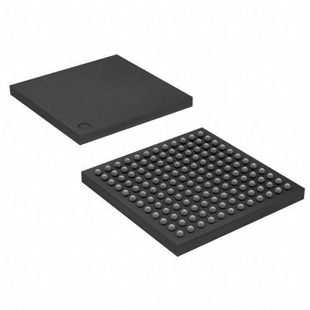
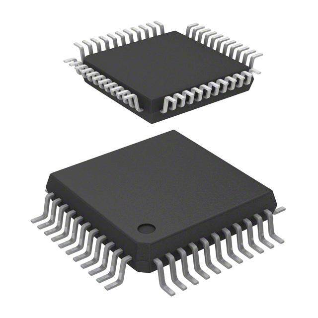
LPC11E1x NXP Semiconductors 32-bit ARM Cortex-M0 microcontroller Unique device serial number for identification. Single 3.3V power supply (1.8V to 3.6V). Temperature range 40 C to +85 C. Available as LQFP64, LQFP48, and HVQFN33 package. 3. Applications Consumer peripherals Handheld scanners Medical Industrial control 4. Ordering information Table 1. Ordering info rmation Type number Package Name Description Version LPC11E11FHN33/101 HVQFN33 plastic thermal enhanced very thin quad flat package; no leads; 33 n/a terminals; body 7 7 0.85 mm LPC11E12FBD48/201 LQFP48 plastic low profile quad flat package; 48 leads; body 7 7 1.4 mm SOT313-2 LPC11E13FBD48/301 LQFP48 plastic low profile quad flat package; 48 leads; body 7 7 1.4 mm SOT313-2 LPC11E14FHN33/401 HVQFN33 plastic thermal enhanced very thin quad flat package; no leads; 33 n/a terminals; body 7 7 0.85 mm LPC11E14FBD48/401 LQFP48 plastic low profile quad flat package; 48 leads; body 7 7 1.4 mm SOT313-2 LPC11E14FBD64/401 LQFP64 plastic low profile quad flat package; 64 leads; body 10 10 1.4 mm SOT314-2 4.1 Ordering options Table 2. Part ordering options Part Number Flash EEPROM SRAM I2C-bus USART SSP ADC GPIO FM+ channels LPC11E11FHN33/101 8 kB 512 B 4 kB 1 1 2 8 28 LPC11E12FBD48/201 16 kB 1 kB 6 kB 1 1 2 8 40 LPC11E13FBD48/301 24 kB 2 kB 8 kB 1 1 2 8 40 LPC11E14FHN33/401 32 kB 4 kB 10 kB 1 1 2 8 28 LPC11E14FBD48/401 32 kB 4 kB 10 kB 1 1 2 8 40 LPC11E14FBD64/401 32 kB 4 kB 10 kB 1 1 2 8 54 LPC11E1X All information provided in this document is subject to legal disclaimers. © NXP B.V. 2013. All rights reserved. Product data sheet Rev. 1.1 — 24 September 2013 3 of 62
LPC11E1x NXP Semiconductors 32-bit ARM Cortex-M0 microcontroller 5. Block diagram SWD, JTAG XTALIN XTALOUT RESET LPC11E1x SYSTEM OSCILLATOR TEST/DEBUG CLOCK INTERFACE IRC, WDO GENERATION, POWER CONTROL, CLKOUT ARM BOD SYSTEM FUNCTIONS CORTEX-M0 POR EEPROM PLL0 512 B 1/2/4 kB FLASH SRAM ROM system bus 8/16/24/32 kB 4/6/8/10 kB 16 kB slave slave slave slave HIGH-SPEED GPIO ports 0/1 AHB-LITE BUS GPIO slave AHB TO APB BRIDGE RXD TXD DCD, DSR(1), RI(1) USART/ 10-bit ADC AD[7:0] SMARTCARD INTERFACE CTS, RTS, DTR SCLK I2C-BUS SCL, SDA CT16B0_MAT[2:0] 16-bit COUNTER/TIMER 0 CT16B0_CAP[1:0](2) SCK0, SSEL0, CT16B1_MAT[1:0] SSP0 MISO0, MOSI0 16-bit COUNTER/TIMER 1 CT16B1_CAP[1:0](2) SCK1, SSEL1, CT32B0_MAT[3:0] SSP1 32-bit COUNTER/TIMER 0 MISO1, MOSI1 CT32B0_CAP[1:0](2) IOCON CT32B1_MAT[3:0] 32-bit COUNTER/TIMER 1 CT32B1_CAP[1:0](2) SYSTEM CONTROL WINDOWED WATCHDOG TIMER PMU GPIO pins GPIO INTERRUPTS GPIO pins GPIO GROUP0 INTERRUPTS GPIO pins GPIO GROUP1 INTERRUPTS 002aag683 (1) Not available on HVQFN33 packages. (2) CT16B0/1_CAP1, CT32B1_CAP1 available on the LQFP64 package only. CT32B0_CAP1 available on the LQFP64 and LQFP48 packages only. Fig 1. Block diagram LPC11E1X All information provided in this document is subject to legal disclaimers. © NXP B.V. 2013. All rights reserved. Product data sheet Rev. 1.1 — 24 September 2013 4 of 62
LPC11E1x NXP Semiconductors 32-bit ARM Cortex-M0 microcontroller 6. Pinning information 6.1 Pinning P U 2 CLK CK1 AKE MAT S S W _ MAT1 MAT0 CAP0/ MAT2/ MAT3/ T32B1 XD/CT32B0_ XD/CT32B0_ TS/CT32B0_ CD/CT16B0_ D7 D5/CT32B1_ O0_15/AD4/C 19/T 18/R 17/R 15/D 23/A 16/A O/PI itnedrmexin aarle 1a PIO0_ PIO0_ PIO0_ VDD PIO1_ PIO0_ PIO0_ SWDI 2 1 0 9 8 7 6 5 3 3 3 2 2 2 2 2 PIO1_19/DTR/SSEL1 1 24 TRST/PIO0_14/AD3/CT32B1_MAT1 RESET/PIO0_0 2 23 TDO/PIO0_13/AD2/CT32B1_MAT0 PIO0_1/CLKOUT/CT32B0_MAT2 3 22 TMS/PIO0_12/AD1/CT32B1_CAP0 XTALIN 4 LPC11E11 21 TDI/PIO0_11/AD0/CT32B0_MAT3 LPC11E14 XTALOUT 5 20 PIO0_22/AD6/CT16B1_MAT1/MISO1 VDD 6 19 SWCLK/PIO0_10/SCK0/CT16B0_MAT2 PIO0_20/CT16B1_CAP0 7 33 VSS 18 PIO0_9/MOSI0/CT16B0_MAT1 PIO0_2/SSEL0/CT16B0_CAP0 8 17 PIO0_8/MISO0/CT16B0_MAT0 9 10 11 12 13 14 15 16 3 L A 1 1 0 0 S PIO0_ O0_4/SC O0_5/SD T0/MOSI T1/SSEL B0_MAT 0_6/SCK O0_7/CT 002aag684 PI PI MA MA T32 PIO PI _ _ C B1 B1 4/ 6 6 2 1 1 _ T T 1 C C O 1/ 3/ PI 2 2 _ _ 0 1 O O PI PI Transparent top view Fig 2. Pin configuration (HVQFN33) LPC11E1X All information provided in this document is subject to legal disclaimers. © NXP B.V. 2013. All rights reserved. Product data sheet Rev. 1.1 — 24 September 2013 5 of 62
LPC11E1x NXP Semiconductors 32-bit ARM Cortex-M0 microcontroller P U 2 CLK CK1 AKE MAT XD S S W _ R 16/RI/CT16B0_CAP0 19/TXD/CT32B0_MAT1 18/RXD/CT32B0_MAT0 17/RTS/CT32B0_CAP0/ 15/DCD/CT16B0_MAT2/ 23/AD7 16/AD5/CT32B1_MAT3/ O/PIO0_15/AD4/CT32B1 22/RI/MOSI1 14/DSR/CT16B0_MAT1/ PIO1_ PIO0_ PIO0_ PIO0_ VDD PIO1_ PIO0_ VSS PIO0_ SWDI PIO1_ PIO1_ 8 7 6 5 4 3 2 1 0 9 8 7 4 4 4 4 4 4 4 4 4 3 3 3 PIO1_25/CT32B0_MAT1 1 36 PIO1_13/DTR/CT16B0_MAT0/TXD PIO1_19/DTR/SSEL1 2 35 TRST/PIO0_14/AD3/CT32B1_MAT1 RESET/PIO0_0 3 34 TDO/PIO0_13/AD2/CT32B1_MAT0 PIO0_1/CLKOUT/CT32B0_MAT2 4 33 TMS/PIO0_12/AD1/CT32B1_CAP0 VSS 5 32 TDI/PIO0_11/AD0/CT32B0_MAT3 XTALIN 6 LPC11E12FBD48/201 31 PIO1_29/SCK0/CT32B0_CAP1 XTALOUT 7 LPC11E13FBD48/301 30 PIO0_22/AD6/CT16B1_MAT1/MISO1 LPC11E14FBD48/401 VDD 8 29 SWCLK/PIO0_10/SCK0/CT16B0_MAT2 PIO0_20/CT16B1_CAP0 9 28 PIO0_9/MOSI0/CT16B0_MAT1 PIO0_2/SSEL0/CT16B0_CAP0 10 27 PIO0_8/MISO0/CT16B0_MAT0 PIO1_26/CT32B0_MAT2/RXD 11 26 PIO1_21/DCD/MISO1 PIO1_27/CT32B0_MAT3/TXD 12 25 PIO1_31 3 4 5 6 7 8 9 0 1 2 3 4 1 1 1 1 1 1 1 2 2 2 2 2 002aag685 O1_20/DSR/SCK1 PIO0_3 PIO0_4/SCL PIO0_5/SDA 6B1_MAT0/MOSI1 6B1_MAT1/SSEL1 n.c. n.c. 24/CT32B0_MAT0 PIO0_6/SCK0 PIO0_7/CTS 32B0_CAP0/SCLK PI 1/CT1 3/CT1 PIO1_ 28/CT 2 2 _ _ _ 1 0 1 O PIO PIO PI Fig 3. Pin configuration (LQFP48) LPC11E1X All information provided in this document is subject to legal disclaimers. © NXP B.V. 2013. All rights reserved. Product data sheet Rev. 1.1 — 24 September 2013 6 of 62
LPC11E1x NXP Semiconductors 32-bit ARM Cortex-M0 microcontroller 5 1 _ 0 O 6 16 19 18 17 12 15 23 9 16 O/PI 22 3 14 PIO1_ PIO1_ PIO0_ PIO0_ PIO0_ PIO1_ VDD PIO1_ PIO0_ PIO1_ VSS PIO0_ SWDI PIO1_ PIO1_ PIO1_ 4 3 2 1 0 9 8 7 6 5 4 3 2 1 0 9 6 6 6 6 6 5 5 5 5 5 5 5 5 5 5 4 PIO1_0 1 48 VDD PIO1_25 2 47 PIO1_13 PIO1_19 3 46 TRST/PIO0_14 RESET/PIO0_0 4 45 TDO/PIO0_13 PIO0_1 5 44 TMS/PIO0_12 PIO1_7 6 43 PIO1_11 VSS 7 42 TDI/PIO0_11 XTALIN 8 41 PIO1_29 LPC11E14FBD64/401 XTALOUT 9 40 PIO0_22 VDD 10 39 PIO1_8 PIO0_20 11 38 SWCLK/PIO0_10 PIO1_10 12 37 PIO0_9 PIO0_2 13 36 PIO0_8 PIO1_26 14 35 PIO1_21 PIO1_27 15 34 PIO1_2 PIO1_4 16 33 VDD 7 8 9 0 1 2 3 4 5 6 7 8 9 0 1 2 1 1 1 2 2 2 2 2 2 2 2 2 2 3 3 3 002aag686 1_1 _20 0_3 0_4 0_5 _21 _17 _23 n.c. n.c. _24 _18 0_6 0_7 _28 1_5 O 1 O O O 0 1 1 1 1 O O 1 O PI PIO PI PI PI PIO PIO PIO PIO PIO PI PI PIO PI See Table3 for the full pin name. Fig 4. Pin configuration (LQFP64) LPC11E1X All information provided in this document is subject to legal disclaimers. © NXP B.V. 2013. All rights reserved. Product data sheet Rev. 1.1 — 24 September 2013 7 of 62
LPC11E1x NXP Semiconductors 32-bit ARM Cortex-M0 microcontroller 6.2 Pin description Table3 shows all pins and their assigned digital or analog functions in order of the GPIO port number. The default function after reset is listed first. All port pins have internal pull-up resistors enabled after reset except for the true open-drain pins PIO0_4 and PIO0_5. Every port pin has a corresponding IOCON register for programming the digital or analog function, the pull-up/pull-down configuration, the repeater, and the open-drain modes. The USART, counter/timer, and SSP functions are available on more than one port pin. Table 3. Pin descripti on Symbol 3 Reset Type Description N3 48 64 state QF FP FP [1] V Q Q H L L RESET/PIO0_0 2 3 4 [2] I; PU I RESET — External reset input with 20 ns glitch filter. A LOW-going pulse as short as 50 ns on this pin resets the device, causing I/O ports and peripherals to take on their default states, and processor execution to begin at address 0. This pin also serves as the debug select input. LOW level selects the JTAG boundary scan. HIGH level selects the ARM SWD debug mode. - I/O PIO0_0 — General purpose digital input/output pin. PIO0_1/CLKOUT/ 3 4 5 [3] I; PU I/O PIO0_1 — General purpose digital input/output pin. A LOW CT32B0_MAT2 level on this pin during reset starts the ISP command handler. - O CLKOUT — Clockout pin. - O CT32B0_MAT2 — Match output 2 for 32-bit timer 0. PIO0_2/SSEL0/ 8 10 13 [3] I; PU I/O PIO0_2 — General purpose digital input/output pin. CT16B0_CAP0 - I/O SSEL0 — Slave select for SSP0. - I CT16B0_CAP0 — Capture input 0 for 16-bit timer 0. PIO0_3 9 14 19 [3] I; PU I/O PIO0_3 — General purpose digital input/output pin. PIO0_4/SCL 10 15 20 [4] I; IA I/O PIO0_4 — General purpose digital input/output pin (open-drain). - I/O SCL — I2C-bus clock input/output (open-drain). High-current sink only if I2C Fast-mode Plus is selected in the I/O configuration register. PIO0_5/SDA 11 16 21 [4] I; IA I/O PIO0_5 — General purpose digital input/output pin (open-drain). - I/O SDA — I2C-bus data input/output (open-drain). High-current sink only if I2C Fast-mode Plus is selected in the I/O configuration register. PIO0_6/SCK0 15 22 29 [3] I; PU I/O PIO0_6 — General purpose digital input/output pin. - I/O SCK0 — Serial clock for SSP0. PIO0_7/CTS 16 23 30 [5] I; PU I/O PIO0_7 — General purpose digital input/output pin (high-current output driver). - I CTS — Clear To Send input for USART. LPC11E1X All information provided in this document is subject to legal disclaimers. © NXP B.V. 2013. All rights reserved. Product data sheet Rev. 1.1 — 24 September 2013 8 of 62
LPC11E1x NXP Semiconductors 32-bit ARM Cortex-M0 microcontroller Table 3. Pin description Symbol 3 Reset Type Description N3 48 64 state QF FP FP [1] V Q Q H L L PIO0_8/MISO0/ 17 27 36 [3] I; PU I/O PIO0_8 — General purpose digital input/output pin. CT16B0_MAT0 - I/O MISO0 — Master In Slave Out for SSP0. - O CT16B0_MAT0 — Match output 0 for 16-bit timer 0. PIO0_9/MOSI0/ 18 28 37 [3] I; PU I/O PIO0_9 — General purpose digital input/output pin. CT16B0_MAT1 - I/O MOSI0 — Master Out Slave In for SSP0. - O CT16B0_MAT1 — Match output 1 for 16-bit timer 0. SWCLK/PIO0_10/SCK0/ 19 29 38 [3] I; PU I SWCLK — Serial wire clock and test clock TCK for JTAG CT16B0_MAT2 interface. - I/O PIO0_10 — General purpose digital input/output pin. - O SCK0 — Serial clock for SSP0. - O CT16B0_MAT2 — Match output 2 for 16-bit timer 0. TDI/PIO0_11/AD0/ 21 32 42 [6] I; PU I TDI — Test Data In for JTAG interface. CT32B0_MAT3 - I/O PIO0_11 — General purpose digital input/output pin. - I AD0 — A/D converter, input 0. - O CT32B0_MAT3 — Match output 3 for 32-bit timer 0. TMS/PIO0_12/AD1/ 22 33 44 [6] I; PU I TMS — Test Mode Select for JTAG interface. CT32B1_CAP0 - I/O PIO_12 — General purpose digital input/output pin. - I AD1 — A/D converter, input 1. - I CT32B1_CAP0 — Capture input 0 for 32-bit timer 1. TDO/PIO0_13/AD2/ 23 34 45 [6] I; PU O TDO — Test Data Out for JTAG interface. CT32B1_MAT0 - I/O PIO0_13 — General purpose digital input/output pin. - I AD2 — A/D converter, input 2. - O CT32B1_MAT0 — Match output 0 for 32-bit timer 1. TRST/PIO0_14/AD3/ 24 35 46 [6] I; PU I TRST — Test Reset for JTAG interface. CT32B1_MAT1 - I/O PIO0_14 — General purpose digital input/output pin. - I AD3 — A/D converter, input 3. - O CT32B1_MAT1 — Match output 1 for 32-bit timer 1. SWDIO/PIO0_15/AD4/ 25 39 52 [6] I; PU I/O SWDIO — Serial wire debug input/output. CT32B1_MAT2 - I/O PIO0_15 — General purpose digital input/output pin. - I AD4 — A/D converter, input 4. - O CT32B1_MAT2 — Match output 2 for 32-bit timer 1. PIO0_16/AD5/ 26 40 53 [6] I; PU I/O PIO0_16 — General purpose digital input/output pin. CT32B1_MAT3/WAKEUP - I AD5 — A/D converter, input 5. - O CT32B1_MAT3 — Match output 3 for 32-bit timer 1. - I WAKEUP — Deep power-down mode wake-up pin with 20 ns glitch filter. Pull this pin HIGH externally to enter Deep power-down mode. Pull this pin LOW to exit Deep power-down mode. A LOW-going pulse as short as 50 ns wakes up the part. LPC11E1X All information provided in this document is subject to legal disclaimers. © NXP B.V. 2013. All rights reserved. Product data sheet Rev. 1.1 — 24 September 2013 9 of 62
LPC11E1x NXP Semiconductors 32-bit ARM Cortex-M0 microcontroller Table 3. Pin description Symbol 3 Reset Type Description N3 48 64 state QF FP FP [1] V Q Q H L L PIO0_17/RTS/ 30 45 60 [3] I; PU I/O PIO0_17 — General purpose digital input/output pin. CT32B0_CAP0/SCLK - O RTS — Request To Send output for USART. - I CT32B0_CAP0 — Capture input 0 for 32-bit timer 0. - I/O SCLK — Serial clock input/output for USART in synchronous mode. PIO0_18/RXD/ 31 46 61 [3] I; PU I/O PIO0_18 — General purpose digital input/output pin. CT32B0_MAT0 - I RXD — Receiver input for USART. Used in UART ISP mode. - O CT32B0_MAT0 — Match output 0 for 32-bit timer 0. PIO0_19/TXD/ 32 47 62 [3] I; PU I/O PIO0_19 — General purpose digital input/output pin. CT32B0_MAT1 - O TXD — Transmitter output for USART. Used in UART ISP mode. - O CT32B0_MAT1 — Match output 1 for 32-bit timer 0. PIO0_20/CT16B1_CAP0 7 9 11 [3] I; PU I/O PIO0_20 — General purpose digital input/output pin. - I CT16B1_CAP0 — Capture input 0 for 16-bit timer 1. PIO0_21/CT16B1_MAT0/ 12 17 22 [3] I; PU I/O PIO0_21 — General purpose digital input/output pin. MOSI1 - O CT16B1_MAT0 — Match output 0 for 16-bit timer 1. - I/O MOSI1 — Master Out Slave In for SSP1. PIO0_22/AD6/ 20 30 40 [6] I; PU I/O PIO0_22 — General purpose digital input/output pin. CT16B1_MAT1/MISO1 - I AD6 — A/D converter, input 6. - O CT16B1_MAT1 — Match output 1 for 16-bit timer 1. - I/O MISO1 — Master In Slave Out for SSP1. PIO0_23/AD7 27 42 56 [6] I; PU I/O PIO0_23 — General purpose digital input/output pin. - I AD7 — A/D converter, input 7. PIO1_0/CT32B1_MAT0 - - 1 [3] I; PU I/O PIO1_0 — General purpose digital input/output pin. - O CT32B1_MAT0 — Match output 0 for 32-bit timer 1. PIO1_1/CT32B1_MAT1 - - 17 [3] I; PU I/O PIO1_1 — General purpose digital input/output pin. - O CT32B1_MAT1 — Match output 1 for 32-bit timer 1. PIO1_2/CT32B1_MAT2 - - 34 [3] I; PU I/O PIO1_2 — General purpose digital input/output pin. - O CT32B1_MAT2 — Match output 2 for 32-bit timer 1. PIO1_3/CT32B1_MAT3 - - 50 [3] I; PU I/O PIO1_3 — General purpose digital input/output pin. - O CT32B1_MAT3 — Match output 3 for 32-bit timer 1. PIO1_4/CT32B1_CAP0 - - 16 [3] I; PU I/O PIO1_4 — General purpose digital input/output pin. - I CT32B1_CAP0 — Capture input 0 for 32-bit timer 1. PIO1_5/CT32B1_CAP1 - - 32 [3] I; PU I/O PIO1_5 — General purpose digital input/output pin. - I CT32B1_CAP1 — Capture input 1 for 32-bit timer 1. PIO1_6 - - 64 [3] I; PU I/O PIO1_6 — General purpose digital input/output pin. PIO1_7 - - 6 [3] I; PU I/O PIO1_7 — General purpose digital input/output pin. PIO1_8 - - 39 [3] I; PU I/O PIO1_8 — General purpose digital input/output pin. LPC11E1X All information provided in this document is subject to legal disclaimers. © NXP B.V. 2013. All rights reserved. Product data sheet Rev. 1.1 — 24 September 2013 10 of 62
LPC11E1x NXP Semiconductors 32-bit ARM Cortex-M0 microcontroller Table 3. Pin description Symbol 3 Reset Type Description N3 48 64 state QF FP FP [1] V Q Q H L L PIO1_9 - - 55 [3] I; PU I/O PIO1_9 — General purpose digital input/output pin. PIO1_10 - - 12 [3] I; PU I/O PIO1_10 — General purpose digital input/output pin. PIO1_11 - - 43 [3] I; PU I/O PIO1_11 — General purpose digital input/output pin. PIO1_12 - - 59 [3] I; PU I/O PIO1_12 — General purpose digital input/output pin. PIO1_13/DTR/ - 36 47 [3] I; PU I/O PIO1_13 — General purpose digital input/output pin. CT16B0_MAT0/TXD - O DTR — Data Terminal Ready output for USART. - O CT16B0_MAT0 — Match output 0 for 16-bit timer 0. - O TXD — Transmitter output for USART. PIO1_14/DSR/ - 37 49 [3] I; PU I/O PIO1_14 — General purpose digital input/output pin. CT16B0_MAT1/RXD - I DSR — Data Set Ready input for USART. - O CT16B0_MAT1 — Match output 1 for 16-bit timer 0. - I RXD — Receiver input for USART. PIO1_15/DCD/ 28 43 57 [3] I; PU I/O PIO1_15 — General purpose digital input/output pin. CT16B0_MAT2/SCK1 I DCD — Data Carrier Detect input for USART. - O CT16B0_MAT2 — Match output 2 for 16-bit timer 0. - I/O SCK1 — Serial clock for SSP1. PIO1_16/RI/ - 48 63 [3] I; PU I/O PIO1_16 — General purpose digital input/output pin. CT16B0_CAP0 - I RI — Ring Indicator input for USART. - I CT16B0_CAP0 — Capture input 0 for 16-bit timer 0. PIO1_17/CT16B0_CAP1/ - - 23 [3] I; PU I/O PIO1_17 — General purpose digital input/output pin. RXD - I CT16B0_CAP1 — Capture input 1 for 16-bit timer 0. - I RXD — Receiver input for USART. PIO1_18/CT16B1_CAP1/ - - 28 [3] I; PU I/O PIO1_18 — General purpose digital input/output pin. TXD - I CT16B1_CAP1 — Capture input 1 for 16-bit timer 1. - O TXD — Transmitter output for USART. PIO1_19/DTR/SSEL1 1 2 3 [3] I; PU I/O PIO1_19 — General purpose digital input/output pin. - O DTR — Data Terminal Ready output for USART. - I/O SSEL1 — Slave select for SSP1. PIO1_20/DSR/SCK1 - 13 18 [3] I; PU I/O PIO1_20 — General purpose digital input/output pin. - I DSR — Data Set Ready input for USART. - I/O SCK1 — Serial clock for SSP1. PIO1_21/DCD/MISO1 - 26 35 [3] I; PU I/O PIO1_21 — General purpose digital input/output pin. - I DCD — Data Carrier Detect input for USART. - I/O MISO1 — Master In Slave Out for SSP1. PIO1_22/RI/MOSI1 - 38 51 [3] I; PU I/O PIO1_22 — General purpose digital input/output pin. - I RI — Ring Indicator input for USART. - I/O MOSI1 — Master Out Slave In for SSP1. LPC11E1X All information provided in this document is subject to legal disclaimers. © NXP B.V. 2013. All rights reserved. Product data sheet Rev. 1.1 — 24 September 2013 11 of 62
LPC11E1x NXP Semiconductors 32-bit ARM Cortex-M0 microcontroller Table 3. Pin description Symbol 3 Reset Type Description N3 48 64 state QF FP FP [1] V Q Q H L L PIO1_23/CT16B1_MAT1/ 13 18 24 [3] I; PU I/O PIO1_23 — General purpose digital input/output pin. SSEL1 - O CT16B1_MAT1 — Match output 1 for 16-bit timer 1. - I/O SSEL1 — Slave select for SSP1. PIO1_24/CT32B0_MAT0 14 21 27 [3] I; PU I/O PIO1_24 — General purpose digital input/output pin. - O CT32B0_MAT0 — Match output 0 for 32-bit timer 0. PIO1_25/CT32B0_MAT1 - 1 2 [3] I; PU I/O PIO1_25 — General purpose digital input/output pin. - O CT32B0_MAT1 — Match output 1 for 32-bit timer 0. PIO1_26/CT32B0_MAT2/ - 11 14 [3] I; PU I/O PIO1_26 — General purpose digital input/output pin. RXD - O CT32B0_MAT2 — Match output 2 for 32-bit timer 0. - I RXD — Receiver input for USART. PIO1_27/CT32B0_MAT3/ - 12 15 [3] I; PU I/O PIO1_27 — General purpose digital input/output pin. TXD - O CT32B0_MAT3 — Match output 3 for 32-bit timer 0. - O TXD — Transmitter output for USART. PIO1_28/CT32B0_CAP0/ - 24 31 [3] I; PU I/O PIO1_28 — General purpose digital input/output pin. SCLK - I CT32B0_CAP0 — Capture input 0 for 32-bit timer 0. - I/O SCLK — Serial clock input/output for USART in synchronous mode. PIO1_29/SCK0/ - 31 41 [3] I; PU I/O PIO1_29 — General purpose digital input/output pin. CT32B0_CAP1 - I/O SCK0 — Serial clock for SSP0. - I CT32B0_CAP1 — Capture input 1 for 32-bit timer 0. PIO1_31 - 25 - [3] I; PU I/O PIO1_31 — General purpose digital input/output pin. n.c. - 19 25 F - Not connected. n.c. - 20 26 F - Not connected. XTALIN 4 6 8 [7] - - Input to the oscillator circuit and internal clock generator circuits. Input voltage must not exceed 1.8V. XTALOUT 5 7 9 [7] - - Output from the oscillator amplifier. V 6; 8; 10; - - Supply voltage to the internal regulator, the external rail, DD 29 44 33; and the ADC. Also used as the ADC reference voltage. 48; 58 V 33 5; 7; - - Ground. SS 41 54 [1] Pin state at reset for default function: I = Input; O = Output; PU = internal pull-up enabled; IA = inactive, no pull-up/down enabled; F = floating; If the pins are not used, tie floating pins to ground or power to minimize power consumption. [2] 5 V tolerant pad. RESET functionality is not available in Deep power-down mode. Use the WAKEUP pin to reset the chip and wake up from Deep power-down mode. An external pull-up resistor is required on this pin for the Deep power-down mode. See Figure28 for the reset pad configuration. [3] 5 V tolerant pad providing digital I/O functions with configurable pull-up/pull-down resistors and configurable hysteresis (see Figure27). [4] I2C-bus pins compliant with the I2C-bus specification for I2C standard mode, I2C Fast-mode, and I2C Fast-mode Plus. [5] 5 V tolerant pad providing digital I/O functions with configurable pull-up/pull-down resistors and configurable hysteresis (see Figure27); includes high-current output driver. LPC11E1X All information provided in this document is subject to legal disclaimers. © NXP B.V. 2013. All rights reserved. Product data sheet Rev. 1.1 — 24 September 2013 12 of 62
LPC11E1x NXP Semiconductors 32-bit ARM Cortex-M0 microcontroller [6] 5 V tolerant pad providing digital I/O functions with configurable pull-up/pull-down resistors, configurable hysteresis, and analog input. When configured as a ADC input, digital section of the pad is disabled and the pin is not 5 V tolerant (see Figure27); includes digital input glitch filter. [7] When the system oscillator is not used, connect XTALIN and XTALOUT as follows: XTALIN can be left floating or can be grounded (grounding is preferred to reduce susceptibility to noise). Leave XTALOUT floating. LPC11E1X All information provided in this document is subject to legal disclaimers. © NXP B.V. 2013. All rights reserved. Product data sheet Rev. 1.1 — 24 September 2013 13 of 62
LPC11E1x NXP Semiconductors 32-bit ARM Cortex-M0 microcontroller 7. Functional description 7.1 On-chip flash programming memory The LPC11E1x contain 24 kB or 32 kB on-chip flash program memory. The flash can be programmed using In-System Programming (ISP) or In-Application Programming (IAP) via the on-chip boot loader software. 7.2 EEPROM The LPC11E1x contain 500 Byte, 1 kB, 2 kB, or 4 kB of on-chip byte-erasable and byte-programmable EEPROM data memory. The EEPROM can be programmed using In-Application Programming (IAP) via the on-chip boot loader software. 7.3 SRAM The LPC11E1x contain a total of 4 kB, 6 kB, 8 kB, or 10 kB on-chip static RAM memory. 7.4 On-chip ROM The on-chip ROM contains the boot loader and the following Application Programming Interfaces (APIs): • In-System Programming (ISP) and In-Application Programming (IAP) support for flash • IAP support for EEPROM • Power profiles for configuring power consumption and PLL settings • 32-bit integer division routines 7.5 Memory map The LPC11E1x incorporates several distinct memory regions, shown in the following figures. Figure5 shows the overall map of the entire address space from the user program viewpoint following reset. The interrupt vector area supports address remapping. The AHB peripheral area is 2 MB in size and is divided to allow for up to 128 peripherals. The APB peripheral area is 512 kB in size and is divided to allow for up to 32 peripherals. Each peripheral of either type is allocated 16kB of space. This addressing scheme allows simplifying the address decoding for each peripheral. LPC11E1X All information provided in this document is subject to legal disclaimers. © NXP B.V. 2013. All rights reserved. Product data sheet Rev. 1.1 — 24 September 2013 14 of 62
LPC11E1x NXP Semiconductors 32-bit ARM Cortex-M0 microcontroller LPC11E1x 4 GB 0xFFFF FFFF reserved 0xE010 0000 private peripheral bus 0xE000 0000 reserved APB peripherals 0x5000 4000 0x4008 0000 GPIO 25 - 31 reserved 0x5000 0000 0x4006 4000 24 GPIO GROUP1 INT 0x4006 0000 reserved 23 GPIO GROUP0 INT 0x4005 C000 22 SSP1 0x4005 8000 0x4008 0000 20 - 21 reserved APB peripherals 0x4004 C000 1 GB 0x4000 0000 19 GPIO interrupts 0x4004 C000 18 system control 0x4004 8000 reserved 17 IOCON 0x4004 4000 16 SSP0 0x4004 0000 0x2000 0800 15 flash/EEPROM controller 0.5 GB 2 kB SRAM (LPC11E14/401) 0x2000 0000 0x4003 C000 14 PMU 0x4003 8000 reserved 10 - 13 reserved 0x1FFF 4000 16 kB boot ROM 0x4002 8000 0x1FFF 0000 9 reserved 0x4002 4000 reserved 8 reserved 0x4002 0000 0x1000 2000 8 kB SRAM (LPC11E13/301 7 ADC 0x4001 C000 LPC11E14/401) 0x1000 1800 6 32-bit counter/timer 1 0x4001 8000 6 kB SRAM (LPC11E12/201) 0x1000 1000 5 32-bit counter/timer 0 0x4001 4000 4 kB SRAM (LPC11E11/101) 0x1000 0000 4 16-bit counter/timer 1 0x4001 0000 3 16-bit counter/timer 0 0x4000 C000 reserved 2 USART/SMART CARD 0x4000 8000 0x0000 8000 1 WWDT 0x4000 4000 32 kB on-chip flash (LPC11E14) 0x0000 6000 0 I2C-bus 0x4000 0000 24 kB on-chip flash (LPC11E13) 0x0000 4000 0x0000 00C0 16 kB on-chip flash (LPC11E12) 0x0000 2000 active interrupt vectors 0x0000 0000 8 kB on-chip flash (LPC11E11) 0 GB 0x0000 0000 002aag688 Fig 5. LPC11E1x memory map 7.6 Nested Vectored Interrupt Controller (NVIC) The Nested Vectored Interrupt Controller (NVIC) is part of the Cortex-M0. The tight coupling to the CPU allows for low interrupt latency and efficient processing of late arriving interrupts. 7.6.1 Features • Controls system exceptions and peripheral interrupts. • In the LPC11E1x, the NVIC supports 24 vectored interrupts. LPC11E1X All information provided in this document is subject to legal disclaimers. © NXP B.V. 2013. All rights reserved. Product data sheet Rev. 1.1 — 24 September 2013 15 of 62
LPC11E1x NXP Semiconductors 32-bit ARM Cortex-M0 microcontroller • Four programmable interrupt priority levels, with hardware priority level masking. • Software interrupt generation. 7.6.2 Interrupt sources Each peripheral device has one interrupt line connected to the NVIC but can have several interrupt flags. Individual interrupt flags can also represent more than one interrupt source. 7.7 IOCON block The IOCON block allows selected pins of the microcontroller to have more than one function. Configuration registers control the multiplexers to allow connection between the pin and the on-chip peripherals. Connect peripherals to the appropriate pins before activating the peripheral and before enabling any related interrupt. . Activity of any enabled peripheral function that is not mapped to a related pin is treated as undefined. 7.7.1 Features • Programmable pull-up, pull-down, or repeater mode. • All GPIO pins (except PIO0_4 and PIO0_5) are pulled up to 3.3 V (V = 3.3 V) if their DD pull-up resistor is enabled. • Programmable pseudo open-drain mode. • Programmable 10 ns glitch filter on pins PIO0_22, PIO0_23, and PIO0_11 to PIO0_16. The glitch filter is turned on by default. • Programmable hysteresis. • Programmable input inverter. 7.8 General-Purpose Input/Output GPIO The GPIO registers control device pin functions that are not connected to a specific peripheral function. Pins can be dynamically configured as inputs or outputs. Multiple outputs can be set or cleared in one write operation. LPC11E1x use accelerated GPIO functions: • GPIO registers are a dedicated AHB peripheral so that the fastest possible I/O timing can be achieved. • Entire port value can be written in one instruction. Any GPIO pin providing a digital function can be programmed to generate an interrupt on a level, a rising or falling edge, or both. The GPIO block consists of three parts: 1. The GPIO ports. 2. The GPIO pin interrupt block to control eight GPIO pins selected as pin interrupts. 3. Two GPIO group interrupt blocks to control two combined interrupts from all GPIO pins. LPC11E1X All information provided in this document is subject to legal disclaimers. © NXP B.V. 2013. All rights reserved. Product data sheet Rev. 1.1 — 24 September 2013 16 of 62
LPC11E1x NXP Semiconductors 32-bit ARM Cortex-M0 microcontroller 7.8.1 Features • GPIO pins can be configured as input or output by software. • All GPIO pins default to inputs with interrupt disabled at reset. • Pin registers allow pins to be sensed and set individually. • Up to eight GPIO pins can be selected from all GPIO pins to create an edge- or level-sensitive GPIO interrupt request. • Any pin or pins in each port can trigger a port interrupt. 7.9 USART The LPC11E1x contain one USART. The USART includes full modem control, support for synchronous mode, and a smart card interface. The RS-485/9-bit mode allows both software address detection and automatic address detection using 9-bit mode. The USART uses a fractional baud rate generator. Standard baud rates such as 115200Bd can be achieved with any crystal frequency above 2MHz. 7.9.1 Features • Maximum USART data bit rate of 3.125Mbit/s. • 16 byte receive and transmit FIFOs. • Register locations conform to 16C550 industry standard. • Receiver FIFO trigger points at 1B, 4B, 8B, and 14B. • Built-in fractional baud rate generator covering wide range of baud rates without a need for external crystals of particular values. • Fractional divider for baud rate control, auto baud capabilities and FIFO control mechanism that enables software flow control implementation. • Support for RS-485/9-bit mode. • Support for modem control. • Support for synchronous mode. • Includes smart card interface. 7.10 SSP serial I/O controller The SSP controllers operate on a SSP, 4-wire SSI, or Microwire bus. It can interact with multiple masters and slaves on the bus. Only a single master and a single slave can communicate on the bus during a given data transfer. The SSP supports full duplex transfers, with frames of 4bit to 16bit of data flowing from the master to the slave and from the slave to the master. In practice, often only one of these data flows carries meaningful data. 7.10.1 Features • Maximum SSP speed of 25 Mbit/s (master) or 4.17 Mbit/s (slave) (in SSP mode) • Compatible with Motorola SPI, 4-wire Texas Instruments SSI, and National Semiconductor Microwire buses LPC11E1X All information provided in this document is subject to legal disclaimers. © NXP B.V. 2013. All rights reserved. Product data sheet Rev. 1.1 — 24 September 2013 17 of 62
LPC11E1x NXP Semiconductors 32-bit ARM Cortex-M0 microcontroller • Synchronous serial communication • Master or slave operation • 8-frame FIFOs for both transmit and receive • 4-bit to 16-bit frame 7.11 I2C-bus serial I/O controller The LPC11E1x contain one I2C-bus controller. The I2C-bus is bidirectional for inter-IC control using only two wires: a Serial Clock line (SCL) and a Serial Data line (SDA). Each device is recognized by a unique address and can operate as either a receiver-only device (e.g., an LCD driver) or a transmitter with the capability to both receive and send information (such as memory). Transmitters and/or receivers can operate in either master or slave mode, depending on whether the chip has to initiate a data transfer or is only addressed. The I2C-bus is a multi-master bus, and more than one bus master connected to the interface can be controlled the bus. 7.11.1 Features • The I2C-interface is an I2C-bus compliant interface with open-drain pins. The I2C-bus interface supports Fast-mode Plus with bit rates up to 1 Mbit/s. • Easy to configure as master, slave, or master/slave. • Programmable clocks allow versatile rate control. • Bidirectional data transfer between masters and slaves. • Multi-master bus (no central master). • Arbitration between simultaneously transmitting masters without corruption of serial data on the bus. • Serial clock synchronization allows devices with different bit rates to communicate via one serial bus. • Serial clock synchronization can be used as a handshake mechanism to suspend and resume serial transfer. • The I2C-bus can be used for test and diagnostic purposes. • The I2C-bus controller supports multiple address recognition and a bus monitor mode. 7.12 10-bit ADC The LPC11E1x contains one ADC. It is a single 10-bit successive approximation ADC with eight channels. 7.12.1 Features • 10-bit successive approximation ADC. • Input multiplexing among 8 pins. • Power-down mode. • Measurement range 0 V to V . DD • 10-bit conversion time 2.44s (up to 400 kSamples/s). • Burst conversion mode for single or multiple inputs. LPC11E1X All information provided in this document is subject to legal disclaimers. © NXP B.V. 2013. All rights reserved. Product data sheet Rev. 1.1 — 24 September 2013 18 of 62
LPC11E1x NXP Semiconductors 32-bit ARM Cortex-M0 microcontroller • Optional conversion on transition of input pin or timer match signal. • Individual result registers for each ADC channel to reduce interrupt overhead. 7.13 General purpose external event counter/timers The LPC11E1x include two 32-bit counter/timers and two 16-bit counter/timers. The counter/timer is designed to count cycles of the system derived clock. It can optionally generate interrupts or perform other actions at specified timer values, based on four match registers. Each counter/timer also includes one capture input to trap the timer value when an input signal transitions, optionally generating an interrupt. 7.13.1 Features • A 32-bit/16-bit timer/counter with a programmable 32-bit/16-bit prescaler. • Counter or timer operation. • Up to two capture channels per timer, that can take a snapshot of the timer value when an input signal transitions. A capture event can also generate an interrupt. • Four match registers per timer that allow: – Continuous operation with optional interrupt generation on match. – Stop timer on match with optional interrupt generation. – Reset timer on match with optional interrupt generation. • Up to four external outputs corresponding to match registers, with the following capabilities: – Set LOW on match. – Set HIGH on match. – Toggle on match. – Do nothing on match. • The timer and prescaler can be configured to be cleared on a designated capture event. This feature permits easy pulse-width measurement by clearing the timer on the leading edge of an input pulse and capturing the timer value on the trailing edge. 7.14 System tick timer The ARM Cortex-M0 includes a system tick timer (SYSTICK) that is intended to generate a dedicated SYSTICK exception at a fixed time interval (typically 10 ms). 7.15 Windowed WatchDog Timer (WWDT) The purpose of the WWDT is to prevent an unresponsive system state. If software fails to update the watchdog within a programmable time window, the watchdog resets the microcontroller 7.15.1 Features • Internally resets chip if not periodically reloaded during the programmable time-out period. • Optional windowed operation requires reload to occur between a minimum and maximum time period, both programmable. LPC11E1X All information provided in this document is subject to legal disclaimers. © NXP B.V. 2013. All rights reserved. Product data sheet Rev. 1.1 — 24 September 2013 19 of 62
LPC11E1x NXP Semiconductors 32-bit ARM Cortex-M0 microcontroller • Optional warning interrupt can be generated at a programmable time before watchdog time-out. • Software enables the WWDT, but a hardware reset or a watchdog reset/interrupt is required to disable the WWDT. • Incorrect feed sequence causes reset or interrupt, if enabled. • Flag to indicate watchdog reset. • Programmable 24-bit timer with internal prescaler. • Selectable time period from (T 2564) to (T 2244) in cy(WDCLK) cy(WDCLK) multiples of T 4. cy(WDCLK) • The Watchdog Clock (WDCLK) source can be selected from the IRC or the dedicated watchdog oscillator (WDO). The clock source selection provides a wide range of potential timing choices of watchdog operation under different power conditions. 7.16 Clocking and power control 7.16.1 Integrated oscillators The LPC11E1x include three independent oscillators: the system oscillator, the Internal RC oscillator (IRC), and the watchdog oscillator. Each oscillator can be used for more than one purpose as required in a particular application. Following reset, the LPC11E1x operates from the internal RC oscillator until software switches to a different clock source. The IRC allows the system to operate without any external crystal and the bootloader code to operate at a known frequency. See Figure6 for an overview of the LPC11E1x clock generation. LPC11E1X All information provided in this document is subject to legal disclaimers. © NXP B.V. 2013. All rights reserved. Product data sheet Rev. 1.1 — 24 September 2013 20 of 62
LPC11E1x NXP Semiconductors 32-bit ARM Cortex-M0 microcontroller CPU, system control, PMU SYSTEM CLOCK system clock n DIVIDER memories, peripheral clocks SYSAHBCLKCTRLn (AHB clock enable) IRC oscillator main clock SSP0 PERIPHERAL SSP0 CLOCK DIVIDER watchdog oscillator USART PERIPHERAL UART CLOCK DIVIDER MAINCLKSEL (main clock select) SSP1 PERIPHERAL SSP1 CLOCK DIVIDER IRC oscillator SYSTEM PLL IRC oscillator system oscillator system oscillator CLKOUT PIN CLOCK CLKOUT pin watchdog oscillator DIVIDER SYSPLLCLKSEL (system PLL clock select) CLKOUTUEN (CLKOUT update enable) IRC oscillator WDT watchdog oscillator WDCLKSEL (WDT clock select) 002aag687 Fig 6. LPC11E1x clocking generation block diagram 7.16.1.1 Internal RC oscillator The IRC can be used as the clock source for the WDT, and/or as the clock that drives the system PLL and then the CPU. The nominal IRC frequency is 12MHz. Upon power-up, any chip reset, or wake-up from Deep power-down mode, the LPC11E1x use the IRC as the clock source. Software can later switch to one of the other available clock sources. 7.16.1.2 System oscillator The system oscillator can be used as the clock source for the CPU, with or without using the PLL. The system oscillator operates at frequencies of 1MHz to 25MHz. This frequency can be boosted to a higher frequency, up to the maximum CPU operating frequency, by the system PLL. 7.16.1.3 Watchdog oscillator The watchdog oscillator can be used as a clock source that directly drives the CPU, the watchdog timer, or the CLKOUT pin. The watchdog oscillator nominal frequency is programmable between 7.8 kHz and 1.7 MHz. The frequency spread over processing and temperature is 40% (see also Table13). LPC11E1X All information provided in this document is subject to legal disclaimers. © NXP B.V. 2013. All rights reserved. Product data sheet Rev. 1.1 — 24 September 2013 21 of 62
LPC11E1x NXP Semiconductors 32-bit ARM Cortex-M0 microcontroller 7.16.2 System PLL The PLL accepts an input clock frequency in the range of 10MHz to 25MHz. The input frequency is multiplied up to a high frequency with a Current Controlled Oscillator (CCO). The multiplier can be an integer value from 1 to 32. The CCO operates in the range of 156MHz to 320MHz. To support this frequency range, an additional divider keeps the CCO within its frequency range while the PLL is providing the desired output frequency. The output divider can be set to divide by 2, 4, 8, or 16 to produce the output clock. The PLL output frequency must be lower than 100 MHz. Since the minimum output divider value is 2, it is insured that the PLL output has a 50% duty cycle. The PLL is turned off and bypassed following a chip reset. Software can enable the PLL later. The program must configure and activate the PLL, wait for the PLL to lock, and then connect to the PLL as a clock source. The PLL settling time is 100s. 7.16.3 Clock output The LPC11E1x feature a clock output function that routes the IRC oscillator, the system oscillator, the watchdog oscillator, or the main clock to an output pin. 7.16.4 Wake-up process The LPC11E1x begin operation by using the 12MHz IRC oscillator as the clock source at power-up and when awakened from Deep power-down mode . This mechanism allows chip operation to resume quickly. If the application uses the main oscillator or the PLL, software must enable these components and wait for them to stabilize. Only then can the system use the PLL and main oscillator as a clock source. 7.16.5 Power control The LPC11E1x support various power control features. There are four special modes of processor power reduction: Sleep mode, Deep-sleep mode, Power-down mode, and Deep power-down mode. The CPU clock rate can also be controlled as needed by changing clock sources, reconfiguring PLL values, and/or altering the CPU clock divider value. This power control mechanism allows a trade-off of power versus processing speed based on application requirements. In addition, a register is provided for shutting down the clocks to individual on-chip peripherals. This register allows fine-tuning of power consumption by eliminating all dynamic power use in any peripherals that are not required for the application. Selected peripherals have their own clock divider which provides even better power control. 7.16.5.1 Power profiles The power consumption in Active and Sleep modes can be optimized for the application through simple calls to the power profile. The power configuration routine configures the LPC11E1x for one of the following power modes: • Default mode corresponding to power configuration after reset. • CPU performance mode corresponding to optimized processing capability. • Efficiency mode corresponding to optimized balance of current consumption and CPU performance. • Low-current mode corresponding to lowest power consumption. In addition, the power profile includes routines to select the optimal PLL settings for a given system clock and PLL input clock. LPC11E1X All information provided in this document is subject to legal disclaimers. © NXP B.V. 2013. All rights reserved. Product data sheet Rev. 1.1 — 24 September 2013 22 of 62
LPC11E1x NXP Semiconductors 32-bit ARM Cortex-M0 microcontroller 7.16.5.2 Sleep mode When Sleep mode is entered, the clock to the core is stopped. Resumption from the Sleep mode does not need any special sequence but re-enabling the clock to the ARM core. In Sleep mode, execution of instructions is suspended until either a reset or interrupt occurs. Peripheral functions continue operation during Sleep mode and can generate interrupts to cause the processor to resume execution. Sleep mode eliminates dynamic power used by the processor itself, by memory systems and related controllers, and by internal buses. 7.16.5.3 Deep-sleep mode In Deep-sleep mode, the LPC11E1x is in Sleep-mode and all peripheral clocks and all clock sources are off except for the IRC. The IRC output is disabled unless the IRC is selected as input to the watchdog timer. In addition all analog blocks are shut down and the flash is in stand-by mode. In Deep-sleep mode, the application can keep the watchdog oscillator and the BOD circuit running for self-timed wake-up and BOD protection. The LPC11E1x can wake up from Deep-sleep mode via reset, selected GPIO pins, or a watchdog timer interrupt. Deep-sleep mode saves power and allows for short wake-up times. 7.16.5.4 Power-down mode In Power-down mode, the LPC11E1x is in Sleep-mode and all peripheral clocks and all clock sources are off except for watchdog oscillator if selected. In addition all analog blocks and the flash are shut down. In Power-down mode, the application can keep the BOD circuit running for BOD protection. The LPC11E1x can wake up from Power-down mode via reset, selected GPIO pins, or a watchdog timer interrupt. Power-down mode reduces power consumption compared to Deep-sleep mode at the expense of longer wake-up times. 7.16.5.5 Deep power-down mode In Deep power-down mode, power is shut off to the entire chip except for the WAKEUP pin. The LPC11E1x can wake up from Deep power-down mode via the WAKEUP pin. The LPC11E1x can be prevented from entering Deep power-down mode by setting a lock bit in the PMU block. Locking out Deep power-down mode enables the application to keep the watchdog timer or the BOD running at all times. When entering Deep power-down mode, an external pull-up resistor is required on the WAKEUP pin to hold it HIGH. Pull the RESET pin HIGH to prevent it from floating while in Deep power-down mode. LPC11E1X All information provided in this document is subject to legal disclaimers. © NXP B.V. 2013. All rights reserved. Product data sheet Rev. 1.1 — 24 September 2013 23 of 62
LPC11E1x NXP Semiconductors 32-bit ARM Cortex-M0 microcontroller 7.16.6 System control 7.16.6.1 Reset Reset has four sources on the LPC11E1x: the RESET pin, the Watchdog reset, power-on reset (POR), and the BrownOut Detection (BOD) circuit. The RESET pin is a Schmitt trigger input pin. Assertion of chip reset by any source, once the operating voltage attains a usable level, starts the IRC and initializes the flash controller. A LOW-going pulse as short as 50 ns resets the part. When the internal Reset is removed, the processor begins executing at address 0, which is initially the Reset vector mapped from the boot block. At that point, all of the processor and peripheral registers have been initialized to predetermined values. In Deep power-down mode, an external pull-up resistor is required on the RESET pin. 7.16.6.2 Brownout detection The LPC11E1x includes four levels for monitoring the voltage on the V pin. If this DD voltage falls below one of the four selected levels, the BOD asserts an interrupt signal to the NVIC. This signal can be enabled for interrupt in the Interrupt Enable Register in the NVIC to cause a CPU interrupt. Alternatively, software can monitor the signal by reading a dedicated status register. Four additional threshold levels can be selected to cause a forced reset of the chip. 7.16.6.3 Code security (Code Read Protection - CRP) CRP provides different levels of security in the system so that access to the on-chip flash and use of the Serial Wire Debugger (SWD) and In-System Programming (ISP) can be restricted. Programming a specific pattern into a dedicated flash location invokes CRP. IAP commands are not affected by the CRP. In addition, ISP entry via the PIO0_1 pin can be disabled without enabling CRP. For details, see the LPC11Exx user manual. There are three levels of Code Read Protection: 1. CRP1 disables access to the chip via the SWD and allows partial flash update (excluding flash sector 0) using a limited set of the ISP commands. This mode is useful when CRP is required and flash field updates are needed but all sectors cannot be erased. 2. CRP2 disables access to the chip via the SWD and only allows full flash erase and update using a reduced set of the ISP commands. 3. Running an application with level CRP3 selected, fully disables any access to the chip via the SWD pins and the ISP. This mode effectively disables ISP override using PIO0_1 pin as well. If necessary, the application must provide a flash update mechanism using IAP calls or using a call to the reinvoke ISP command to enable a flash update via the USART. LPC11E1X All information provided in this document is subject to legal disclaimers. © NXP B.V. 2013. All rights reserved. Product data sheet Rev. 1.1 — 24 September 2013 24 of 62
LPC11E1x NXP Semiconductors 32-bit ARM Cortex-M0 microcontroller CAUTION If level three Code Read Protection (CRP3) is selected, no future factory testing can be performed on the device. In addition to the three CRP levels, sampling of pin PIO0_1 for valid user code can be disabled. For details, see the LPC11Exx user manual. 7.16.6.4 APB interface The APB peripherals are located on one APB bus. 7.16.6.5 AHBLite The AHBLite connects the CPU bus of the ARM Cortex-M0 to the flash memory, the main static RAM, and the ROM. 7.16.6.6 External interrupt inputs All GPIO pins can be level or edge sensitive interrupt inputs. 7.17 Emulation and debugging Debug functions are integrated into the ARM Cortex-M0. Serial wire debug functions are supported in addition to a standard JTAG boundary scan. The ARM Cortex-M0 is configured to support up to four breakpoints and two watch points. The RESET pin selects between the JTAG boundary scan (RESET = LOW) and the ARM SWD debug (RESET = HIGH). The ARM SWD debug port is disabled while the LPC11E1x is in reset. To perform boundary scan testing, follow these steps: 1. Erase any user code residing in flash. 2. Power up the part with the RESET pin pulled HIGH externally. 3. Wait for at least 250 s. 4. Pull the RESET pin LOW externally. 5. Perform boundary scan operations. 6. Once the boundary scan operations are completed, assert the TRST pin to enable the SWD debug mode, and release the RESET pin (pull HIGH). Remark: The JTAG interface cannot be used for debug purposes. LPC11E1X All information provided in this document is subject to legal disclaimers. © NXP B.V. 2013. All rights reserved. Product data sheet Rev. 1.1 — 24 September 2013 25 of 62
LPC11E1x NXP Semiconductors 32-bit ARM Cortex-M0 microcontroller 8. Limiting values Table 4. Limiting valu es In accordance with the Absolute Maximum Rating System (IEC 60134).[1] Symbol Parameter Conditions Min Max Unit V supply voltage (core and external rail) [2] 0.5 +4.6 V DD V input voltage 5V tolerant digital [5][2] 0.5 +5.5 V I I/O pins; V 1.8 V DD V = 0 V 0.5 +3.6 V DD 5 V tolerant [2][4] 0.5 +5.5 open-drain pins PIO0_4 and PIO0_5 V analog input voltage pin configured as [2] 0.5 4.6 V IA analog input [3] I supply current per supply pin - 100 mA DD I ground current per ground pin - 100 mA SS I I/O latch-up current (0.5V ) < V < - 100 mA latch DD I (1.5V ); DD T < 125C j T storage temperature non-operating [6] 65 +150 C stg T maximum junction temperature - 150 C j(max) P total power dissipation (per package) based on package - 1.5 W tot(pack) heat transfer, not device power consumption V electrostatic discharge voltage human body [7] - +6500 V ESD model; all pins [1] The following applies to the limiting values: a) This product includes circuitry specifically designed for the protection of its internal devices from the damaging effects of excessive static charge. Nonetheless, it is suggested that conventional precautions be taken to avoid applying greater than the rated maximum. b) Parameters are valid over operating temperature range unless otherwise specified. All voltages are with respect to VSS unless otherwise noted. c) The limiting values are stress ratings only. Operating the part at these values is not recommended, and proper operation is not guaranteed. The conditions for functional operation are specified in Table5. [2] Maximum/minimum voltage above the maximum operating voltage (see Table5) and below ground that can be applied for a short time (< 10 ms) to a device without leading to irrecoverable failure. Failure includes the loss of reliability and shorter lifetime of the device. [3] See Table6 for maximum operating voltage. [4] V present or not present. Compliant with the I2C-bus standard. 5.5 V can be applied to this pin when V is powered down. DD DD [5] Including voltage on outputs in 3-state mode. [6] The maximum non-operating storage temperature is different than the temperature for required shelf life which should be determined based on required shelf lifetime. Please refer to the JEDEC spec (J-STD-033B.1) for further details. [7] Human body model: equivalent to discharging a 100pF capacitor through a 1.5k series resistor. LPC11E1X All information provided in this document is subject to legal disclaimers. © NXP B.V. 2013. All rights reserved. Product data sheet Rev. 1.1 — 24 September 2013 26 of 62
LPC11E1x NXP Semiconductors 32-bit ARM Cortex-M0 microcontroller 9. Static characteristics Table 5. Static charac teristics T =40C to +85C, unless otherwise specified. amb Symbol Parameter Conditions Min Typ[1] Max Unit V supply voltage (core 1.8 3.3 3.6 V DD and external rail) I supply current Active mode; V =3.3V; DD DD T =25C; code amb while(1){} executed from flash; system clock=12MHz [2][3][4] - 2 - mA [5][6] system clock=50 MHz [3][4][5] - 7 - mA [6][7] Sleep mode; [2][3][4] - 1 - mA V =3.3V; T =25C; [5][6] DD amb system clock= 12 MHz Deep-sleep mode; V =3.3V; [3] - 360 - A DD T =25C amb Power-down mode; V =3.3V; - 2 - A DD T =25C amb Deep power-down mode; [8] - 220 - nA V =3.3V; T =25C DD amb Standard port pins, RESET I LOW-level input current V =0V; on-chip pull-up resistor - 0.5 10 nA IL I disabled I HIGH-level input V =V ; on-chip pull-down resistor - 0.5 10 nA IH I DD current disabled I OFF-state output V =0V; V =V ; on-chip - 0.5 10 nA OZ O O DD current pull-up/down resistors disabled V input voltage pin configured to provide a digital [9][10] 0 - 5.0 V I function [11] V output voltage output active 0 - V V O DD V HIGH-level input 0.7V - - V IH DD voltage V LOW-level input voltage - - 0.3V V IL DD V hysteresis voltage - 0.4 - V hys V HIGH-level output 2.0 V V 3.6 V; I =4 mA V 0.4 - - V OH DD OH DD voltage 1.8 V V < 2.0 V; I =3 mA V 0.4 - - V DD OH DD V LOW-level output 2.0 V V 3.6 V; I =4 mA - - 0.4 V OL DD OL voltage 1.8 V V < 2.0 V; I =3 mA - - 0.4 V DD OL I HIGH-level output V =V 0.4V; 4 - - mA OH OH DD current 2.0 V V 3.6 V DD 1.8 V V < 2.0 V 3 - - mA DD LPC11E1X All information provided in this document is subject to legal disclaimers. © NXP B.V. 2013. All rights reserved. Product data sheet Rev. 1.1 — 24 September 2013 27 of 62
LPC11E1x NXP Semiconductors 32-bit ARM Cortex-M0 microcontroller Table 5. Static characteristics …continued T =40C to +85C, unless otherwise specified. amb Symbol Parameter Conditions Min Typ[1] Max Unit I LOW-level output V =0.4V 4 - - mA OL OL current 2.0 V V 3.6 V DD 1.8 V V < 2.0 V 3 - - mA DD I HIGH-level short-circuit V =0V [12] - - 45 mA OHS OH output current I LOW-level short-circuit V =V [12] - - 50 mA OLS OL DD output current I pull-down current V =5V 10 50 150 A pd I I pull-up current V =0V; 15 50 85 A pu I 2.0 V V 3.6 V DD 1.8 V V < 2.0 V 10 50 85 A DD V <V <5V 0 0 0 A DD I High-drive output pin (PIO0_7) I LOW-level input current V =0V; on-chip pull-up resistor - 0.5 10 nA IL I disabled I HIGH-level input V =V ; on-chip pull-down resistor - 0.5 10 nA IH I DD current disabled I OFF-state output V =0V; V =V ; on-chip - 0.5 10 nA OZ O O DD current pull-up/down resistors disabled V input voltage pin configured to provide a digital [9][10] 0 - 5.0 V I function [11] V output voltage output active 0 - V V O DD V HIGH-level input 0.7V - - V IH DD voltage V LOW-level input voltage - - 0.3V V IL DD V hysteresis voltage 0.4 - - V hys V HIGH-level output 2.5 V V 3.6 V; I =20 mA V 0.4 - - V OH DD OH DD voltage 1.8 V V < 2.5 V; I =12 mA V 0.4 - - V DD OH DD V LOW-level output 2.0 V V 3.6 V; I =4 mA - - 0.4 V OL DD OL voltage 1.8 V V < 2.0 V; I =3 mA - - 0.4 V DD OL I HIGH-level output V =V 0.4V; 20 - - mA OH OH DD current 2.5 V V 3.6 V DD 1.8 V V < 2.5 V 12 - - mA DD I LOW-level output V =0.4V 4 - - mA OL OL current 2.0 V V 3.6 V DD 1.8 V V < 2.0 V 3 - - mA DD I LOW-level short-circuit V =V [12] - - 50 mA OLS OL DD output current I pull-down current V =5V 10 50 150 A pd I I pull-up current V =0V 15 50 85 A pu I 2.0 V V 3.6 V DD 1.8 V V < 2.0 V 10 50 85 A DD V <V <5V 0 0 0 A DD I LPC11E1X All information provided in this document is subject to legal disclaimers. © NXP B.V. 2013. All rights reserved. Product data sheet Rev. 1.1 — 24 September 2013 28 of 62
LPC11E1x NXP Semiconductors 32-bit ARM Cortex-M0 microcontroller Table 5. Static characteristics …continued T =40C to +85C, unless otherwise specified. amb Symbol Parameter Conditions Min Typ[1] Max Unit I2C-bus pins (PIO0_4 and PIO0_5) V HIGH-level input 0.7V - - V IH DD voltage V LOW-level input voltage - - 0.3V V IL DD V hysteresis voltage - 0.05V - V hys DD I LOW-level output V =0.4V; I2C-bus pins configured 3.5 - - mA OL OL current as standard mode pins 2.0 V V 3.6 V DD 1.8 V V < 2.0 V 3 - - DD I LOW-level output V =0.4V; I2C-bus pins configured 20 - - mA OL OL current as Fast-mode Plus pins 2.0 V V 3.6 V DD 1.8 V V < 2.0 V 16 - - DD I input leakage current V =V [13] - 2 4 A LI I DD V =5V - 10 22 A I Oscillator pins V crystal input voltage 0.5 1.8 1.95 V i(xtal) V crystal output voltage 0.5 1.8 1.95 V o(xtal) Pin capacitance C input/output pins configured for analog function - - 7.1 pF io capacitance I2C-bus pins (PIO0_4 and PIO0_5) - - 2.5 pF pins configured as GPIO - - 2.8 pF [1] Typical ratings are not guaranteed. The values listed are at room temperature (25C), nominal supply voltages. [2] IRC enabled; system oscillator disabled; system PLL disabled. [3] I measurements were performed with all pins configured as GPIO outputs driven LOW and pull-up resistors disabled. DD [4] BOD disabled. [5] All peripherals disabled in the AHBCLKCTRL register. Peripheral clocks to USART, SSP0/1 disabled in the SYSCON block. [6] Low-current mode PWR_LOW_CURRENT selected when running the set_power routine in the power profiles. [7] IRC disabled; system oscillator enabled; system PLL enabled. [8] WAKEUP pin pulled HIGH externally. An external pull-up resistor is required on the RESET pin for the Deep power-down mode. [9] Including voltage on outputs in 3-state mode. [10] V supply voltage must be present. DD [11] 3-state outputs go into 3-state mode in Deep power-down mode. [12] Allowed as long as the current limit does not exceed the maximum current allowed by the device. [13] To V . SS LPC11E1X All information provided in this document is subject to legal disclaimers. © NXP B.V. 2013. All rights reserved. Product data sheet Rev. 1.1 — 24 September 2013 29 of 62
LPC11E1x NXP Semiconductors 32-bit ARM Cortex-M0 microcontroller Table 6. ADC static c haracteristics T =40C to +85C unless otherwise specified; ADC frequency 4.5MHz, V = 2.5 V to 3.6 V. amb DD Symbol Parameter Conditions Min Typ Max Unit V analog input voltage 0 - V V IA DD C analog input capacitance - - 1 pF ia E differential linearity error [1][2] - - 1 LSB D E integral non-linearity [3] - - 1.5 LSB L(adj) E offset error [4] - - 3.5 LSB O E gain error [5] - - 0.6 % G E absolute error [6] - - 4 LSB T R voltage source interface - - 40 k vsi resistance R input resistance [7][8] - - 2.5 M i [1] The ADC is monotonic, there are no missing codes. [2] The differential linearity error (E ) is the difference between the actual step width and the ideal step width. See Figure7. D [3] The integral non-linearity (E ) is the peak difference between the center of the steps of the actual and the ideal transfer curve after L(adj) appropriate adjustment of gain and offset errors. See Figure7. [4] The offset error (E ) is the absolute difference between the straight line which fits the actual curve and the straight line which fits the O ideal curve. See Figure7. [5] The gain error (E ) is the relative difference in percent between the straight line fitting the actual transfer curve after removing offset G error, and the straight line which fits the ideal transfer curve. See Figure7. [6] The absolute error (E ) is the maximum difference between the center of the steps of the actual transfer curve of the non-calibrated T ADC and the ideal transfer curve. See Figure7. [7] Tamb = 25 C; maximum sampling frequency fs = 400kSamples/s and analog input capacitance Cia = 1 pF. [8] Input resistance Ri depends on the sampling frequency fs: Ri = 1 / (fs Cia). LPC11E1X All information provided in this document is subject to legal disclaimers. © NXP B.V. 2013. All rights reserved. Product data sheet Rev. 1.1 — 24 September 2013 30 of 62
LPC11E1x NXP Semiconductors 32-bit ARM Cortex-M0 microcontroller offset gain error error EO EG 1023 1022 1021 1020 1019 1018 (2) 7 code (1) out 6 5 (5) 4 (4) 3 (3) 2 1 1 LSB (ideal) 0 1 2 3 4 5 6 7 1018 1019 1020 1021 1022 1023 1024 VIA (LSBideal) offset error EO VDD − VSS 1 LSB = 1024 002aaf426 (1) Example of an actual transfer curve. (2) The ideal transfer curve. (3) Differential linearity error (ED). (4) Integral non-linearity (EL(adj)). (5) Center of a step of the actual transfer curve. Fig 7. ADC characteristics LPC11E1X All information provided in this document is subject to legal disclaimers. © NXP B.V. 2013. All rights reserved. Product data sheet Rev. 1.1 — 24 September 2013 31 of 62
LPC11E1x NXP Semiconductors 32-bit ARM Cortex-M0 microcontroller 9.1 BOD static characteristics Table 7. BOD static characteristics[1] T =25C. amb Symbol Parameter Conditions Min Typ Max Unit V threshold voltage interrupt level 1 th assertion - 2.22 - V de-assertion - 2.35 - V interrupt level 2 assertion - 2.52 - V de-assertion - 2.66 - V interrupt level 3 assertion - 2.80 - V de-assertion - 2.90 - V reset level 0 assertion - 1.46 - V de-assertion - 1.63 - V reset level 1 assertion - 2.06 - V de-assertion - 2.15 - V reset level 2 assertion - 2.35 - V de-assertion - 2.43 - V reset level 3 assertion - 2.63 - V de-assertion - 2.71 - V [1] Interrupt levels are selected by writing the level value to the BOD control register BODCTRL, see the LPC11Exx user manual. 9.2 Power consumption Power measurements in Active, Sleep, and Deep-sleep modes were performed under the following conditions (see the LPC11Exx user manual): • Configure all pins as GPIO with pull-up resistor disabled in the IOCON block. • Configure GPIO pins as outputs using the GPIOnDIR registers. • Write 0 to all GPIOnDATA registers to drive the outputs LOW. LPC11E1X All information provided in this document is subject to legal disclaimers. © NXP B.V. 2013. All rights reserved. Product data sheet Rev. 1.1 — 24 September 2013 32 of 62
LPC11E1x NXP Semiconductors 32-bit ARM Cortex-M0 microcontroller 002aag749 9 IDD 48 MHz(2) (mA) 6 36 MHz(2) 24 MHz(2) 3 12 MHz(1) 0 1.8 2.4 3.0 3.6 VDD (V) Conditions: V = 3.3 V; Active mode entered executing code while(1){} from flash; internal pull-up DD resistors disabled; BOD disabled; all peripherals disabled in the SYSAHBCLKCTRL register; all peripheral clocks disabled; low-current mode. (1) System oscillator and system PLL disabled; IRC enabled. (2) System oscillator and system PLL enabled; IRC disabled. Fig 8. Typical supply current versus regulator supply voltage V in active mode DD 002aag750 9 IDD 48 MHz(2) (mA) 6 36 MHz(2) 24 MHz(2) 3 12 MHz(1) 0 -40 -15 10 35 60 85 temperature (°C) Conditions: V = 3.3 V; Active mode entered executing code while(1){} from flash; internal pull-up DD resistors disabled; BOD disabled; all peripherals disabled in the SYSAHBCLKCTRL register; all peripheral clocks disabled; low-current mode. (1) System oscillator and system PLL disabled; IRC enabled. (2) System oscillator and system PLL enabled; IRC disabled. Fig 9. Typical supply current versus temperature in Active mode LPC11E1X All information provided in this document is subject to legal disclaimers. © NXP B.V. 2013. All rights reserved. Product data sheet Rev. 1.1 — 24 September 2013 33 of 62
LPC11E1x NXP Semiconductors 32-bit ARM Cortex-M0 microcontroller 002aag751 4 IDD (mA) 3 48 MHz(2) 36 MHz(2) 2 24 MHz(2) 12 MHz(1) 1 0 -40 -15 10 35 60 85 temperature (°C) Conditions: V = 3.3 V; Sleep mode entered from flash; internal pull-up resistors disabled; BOD DD disabled; all peripherals disabled in the SYSAHBCLKCTRL register; all peripheral clocks disabled; low-current mode. (1) System oscillator and system PLL disabled; IRC enabled. (2) System oscillator and system PLL enabled; IRC disabled. Fig 10. Typical supply current versus temperature in Sleep mode 002aag745 385 IDD (µA) 375 VDD = 3.6 V 365 VDD = 3.3 V VDD = 2.0 V 355 VDD = 1.8 V 345 -40 -15 10 35 60 85 temperature (°C) Conditions: BOD disabled; all oscillators and analog blocks turned off in the PDSLEEPCFG register. Fig 11. Typical supply current versus temperature in Deep-sleep mode LPC11E1X All information provided in this document is subject to legal disclaimers. © NXP B.V. 2013. All rights reserved. Product data sheet Rev. 1.1 — 24 September 2013 34 of 62
LPC11E1x NXP Semiconductors 32-bit ARM Cortex-M0 microcontroller 002aag746 20 IDD VDD = 3.6 V, 3.3 V (µA) VDD = 2.0 V VDD = 1.8 V 15 10 5 0 -40 -15 10 35 60 85 temperature (°C) Conditions: BOD disabled; all oscillators and analog blocks turned off in the PDSLEEPCFG register. Fig 12. Typical supply current versus temperature in Power-down mode 002aag747 0.8 IDD VDD = 3.6 V (µA) VDD = 3.3 V 0.6 VDD = 2.0 V VDD = 1.8 V 0.4 0.2 0 -40 -15 10 35 60 85 temperature (°C) Fig 13. Typical supply current versus temperature in Deep power-down mode 9.3 Peripheral power consumption The supply current per peripheral is measured as the difference in supply current between the peripheral block enabled and the peripheral block disabled in the SYSAHBCLKCFG and PDRUNCFG (for analog blocks) registers. All other blocks are disabled in both registers and no code is executed. Measured on a typical sample at T =25 C. Unless amb noted otherwise, the system oscillator and PLL are running in both measurements. The supply currents are shown for system clock frequencies of 12 MHz and 48 MHz. LPC11E1X All information provided in this document is subject to legal disclaimers. © NXP B.V. 2013. All rights reserved. Product data sheet Rev. 1.1 — 24 September 2013 35 of 62
LPC11E1x NXP Semiconductors 32-bit ARM Cortex-M0 microcontroller Table 8. Power consumption for individual analog and digital blocks Peripheral Typical supply current in Notes mA n/a 12 MHz 48 MHz IRC 0.27 - - System oscillator running; PLL off; independent of main clock frequency. System oscillator 0.22 - - IRC running; PLL off; independent of main clock at 12 MHz frequency. Watchdog 0.004 - - System oscillator running; PLL off; independent oscillator at of main clock frequency. 500kHz/2 BOD 0.051 - - Independent of main clock frequency. Main PLL - 0.21 - - ADC - 0.08 0.29 - CLKOUT - 0.12 0.47 Main clock divided by 4 in the CLKOUTDIV register. CT16B0 - 0.02 0.06 - CT16B1 - 0.02 0.06 - CT32B0 - 0.02 0.07 - CT32B1 - 0.02 0.06 - GPIO - 0.23 0.88 GPIO pins configured as outputs and set to LOW. Direction and pin state are maintained if the GPIO is disabled in the SYSAHBCLKCFG register. IOCONFIG - 0.03 0.10 - I2C - 0.04 0.13 - ROM - 0.04 0.15 - SPI0 - 0.12 0.45 - SPI1 - 0.12 0.45 - UART - 0.22 0.82 - WWDT - 0.02 0.06 Main clock selected as clock source for the WDT. LPC11E1X All information provided in this document is subject to legal disclaimers. © NXP B.V. 2013. All rights reserved. Product data sheet Rev. 1.1 — 24 September 2013 36 of 62
LPC11E1x NXP Semiconductors 32-bit ARM Cortex-M0 microcontroller 9.4 Electrical pin characteristics 002aae990 3.6 VOH T = 85 °C (V) 25 °C −40 °C 3.2 2.8 2.4 2 0 10 20 30 40 50 60 IOH (mA) Conditions: V = 3.3 V; on pin PIO0_7. DD Fig 14. High-drive output: Typical HIGH-level output voltage V versus HIGH-level OH output current I . OH 002aaf019 60 IOL T = 85 °C (mA) 25 °C −40 °C 40 20 0 0 0.2 0.4 0.6 VOL (V) Conditions: V = 3.3 V; on pins PIO0_4 and PIO0_5. DD Fig 15. I2C-bus pins (high current sink): Typical LOW-level output current I versus OL LOW-level output voltage V OL LPC11E1X All information provided in this document is subject to legal disclaimers. © NXP B.V. 2013. All rights reserved. Product data sheet Rev. 1.1 — 24 September 2013 37 of 62
LPC11E1x NXP Semiconductors 32-bit ARM Cortex-M0 microcontroller 002aae991 15 IOL T = 85 °C (mA) 25 °C −40 °C 10 5 0 0 0.2 0.4 0.6 VOL (V) Conditions: V = 3.3 V; standard port pins and PIO0_7. DD Fig 16. Typical LOW-level output current I versus LOW-level output voltage V OL OL 002aae992 3.6 VOH (V) T = 85 °C 3.2 25 °C −40 °C 2.8 2.4 2 0 8 16 24 IOH (mA) Conditions: V = 3.3 V; standard port pins. DD Fig 17. Typical HIGH-level output voltage V versus HIGH-level output source current OH I OH LPC11E1X All information provided in this document is subject to legal disclaimers. © NXP B.V. 2013. All rights reserved. Product data sheet Rev. 1.1 — 24 September 2013 38 of 62
LPC11E1x NXP Semiconductors 32-bit ARM Cortex-M0 microcontroller 002aae988 10 Ipu (μA) −10 −30 T = 85 °C 25 °C −40 °C −50 −70 0 1 2 3 4 5 VI (V) Conditions: V = 3.3 V; standard port pins. DD Fig 18. Typical pull-up current I versus input voltage V pu I 002aae989 80 T = 85 °C (μIpAd) −2450 °°CC 60 40 20 0 0 1 2 3 4 5 VI (V) Conditions: V = 3.3 V; standard port pins. DD Fig 19. Typical pull-down current I versus input voltage V pd I LPC11E1X All information provided in this document is subject to legal disclaimers. © NXP B.V. 2013. All rights reserved. Product data sheet Rev. 1.1 — 24 September 2013 39 of 62
LPC11E1x NXP Semiconductors 32-bit ARM Cortex-M0 microcontroller 10. Dynamic characteristics 10.1 Flash memory Table 9. Flash characteristics T =40C to +85C, unless otherwise specified. amb Symbol Parameter Conditions Min Typ Max Unit N endurance [1] 10000 100000 - cycles endu t retention time powered 10 - - years ret unpowered 20 - - years t erase time sector or multiple 95 100 105 ms er consecutive sectors t programming time [2] 0.95 1 1.05 ms prog [1] Number of program/erase cycles. [2] Programming times are given for writing 256 bytes from RAM to the flash. Data must be written to the flash in blocks of 256 bytes. Table 10. EEPROM characteristics T =40Cto+85C; V =2.7Vto3.6V. Based on JEDEC NVM qualification. amb DD Failure rate < 10 ppm for parts as specified below. Symbol Parameter Conditions Min Typ Max Unit N endurance 100000 1000000 - cycles endu t retention time powered 100 200 - years ret unpowered 150 300 - years t programming 64 bytes - 2.9 - ms prog time 10.2 External clock Table 11. Dynamic characteristic: external clock T =40C to +85C; V over specified ranges.[1] amb DD Symbol Parameter Conditions Min Typ[2] Max Unit f oscillator frequency 1 - 25 MHz osc T clock cycle time 40 - 1000 ns cy(clk) t clock HIGH time T 0.4 - - ns CHCX cy(clk) t clock LOW time T 0.4 - - ns CLCX cy(clk) t clock rise time - - 5 ns CLCH t clock fall time - - 5 ns CHCL [1] Parameters are valid over operating temperature range unless otherwise specified. [2] Typical ratings are not guaranteed. The values listed are at room temperature (25C), nominal supply voltages. LPC11E1X All information provided in this document is subject to legal disclaimers. © NXP B.V. 2013. All rights reserved. Product data sheet Rev. 1.1 — 24 September 2013 40 of 62
LPC11E1x NXP Semiconductors 32-bit ARM Cortex-M0 microcontroller tCHCX tCHCL tCLCX tCLCH Tcy(clk) 002aaa907 Fig 20. External clock timing (with an amplitude of at least V = 200mV) i(RMS) 10.3 Internal oscillators Table 12. Dynamic characteristics: IRC T =40C to +85C; 2.7 V V 3.6 V[1]. amb DD Symbol Parameter Conditions Min Typ[2] Max Unit f internal RC oscillator - 11.88 12 12.12 MHz osc(RC) frequency [1] Parameters are valid over operating temperature range unless otherwise specified. [2] Typical ratings are not guaranteed. The values listed are at room temperature (25C), nominal supply voltages. 002aaf403 12.15 f (MHz) VDD = 3.6 V 3.3 V 3.0 V 12.05 2.7 V 2.4 V 2.0 V 11.95 11.85 −40 −15 10 35 60 85 temperature (°C) Conditions: Frequency values are typical values. 12 MHz 1 % accuracy is guaranteed for 2.7 V VDD 3.6 V and Tamb=40C to +85C. Variations between parts may cause the IRC to fall outside the 12 MHz 1 % accuracy specification for voltages below 2.7 V. Fig 21. Internal RC oscillator frequency versus temperature T able 13. Dynamic characteristics: Watchdog oscillator Symbol Parameter Conditions Min Typ[1] Max Unit f internal oscillator DIVSEL = 0x1F, FREQSEL = 0x1 [2][3] - 7.8 - kHz osc(int) frequency in the WDTOSCCTRL register; DIVSEL = 0x00, FREQSEL = 0xF [2][3] - 1700 - kHz in the WDTOSCCTRL register [1] Typical ratings are not guaranteed. The values listed are at nominal supply voltages. LPC11E1X All information provided in this document is subject to legal disclaimers. © NXP B.V. 2013. All rights reserved. Product data sheet Rev. 1.1 — 24 September 2013 41 of 62
LPC11E1x NXP Semiconductors 32-bit ARM Cortex-M0 microcontroller [2] The typical frequency spread over processing and temperature (Tamb = 40C to +85C) is 40 %. [3] See the LPC11Exx user manual. 10.4 I/O pins Table 14. Dynamic characteristics: I/O pins[1] T =40C to +85C; 3.0 V V 3.6 V. amb DD Symbol Parameter Conditions Min Typ Max Unit t rise time pin configured as output 3.0 - 5.0 ns r t fall time pin configured as output 2.5 - 5.0 ns f [1] Applies to standard port pins and RESET pin. 10.5 I2C-bus Table 15. Dynamic cha racteristic: I2C-bus pins[1] T =40C to +85C.[2] amb Symbol Parameter Conditions Min Max Unit f SCL clock Standard-mode 0 100 kHz SCL frequency Fast-mode 0 400 kHz Fast-mode Plus 0 1 MHz t fall time [4][5][6][7] of both SDA and SCL - 300 ns f signals Standard-mode Fast-mode 20 + 0.1 C 300 ns b Fast-mode Plus - 120 ns t LOW period of the Standard-mode 4.7 - s LOW SCL clock Fast-mode 1.3 - s Fast-mode Plus 0.5 - s t HIGH period of the Standard-mode 4.0 - s HIGH SCL clock Fast-mode 0.6 - s Fast-mode Plus 0.26 - s t data hold time [3][4][8] Standard-mode 0 - s HD;DAT Fast-mode 0 - s Fast-mode Plus 0 - s t data set-up time [9][10] Standard-mode 250 - ns SU;DAT Fast-mode 100 - ns Fast-mode Plus 50 - ns [1] See the I2C-bus specification UM10204 for details. [2] Parameters are valid over operating temperature range unless otherwise specified. [3] tHD;DAT is the data hold time that is measured from the falling edge of SCL; applies to data in transmission and the acknowledge. [4] A device must internally provide a hold time of at least 300 ns for the SDA signal (with respect to the V (min) of the SCL signal) to IH bridge the undefined region of the falling edge of SCL. [5] Cb = total capacitance of one bus line in pF. [6] The maximum t for the SDA and SCL bus lines is specified at 300 ns. The maximum fall time for the SDA output stage t is specified at f f 250 ns. This allows series protection resistors to be connected in between the SDA and the SCL pins and the SDA/SCL bus lines without exceeding the maximum specified tf. LPC11E1X All information provided in this document is subject to legal disclaimers. © NXP B.V. 2013. All rights reserved. Product data sheet Rev. 1.1 — 24 September 2013 42 of 62
LPC11E1x NXP Semiconductors 32-bit ARM Cortex-M0 microcontroller [7] In Fast-mode Plus, fall time is specified the same for both output stage and bus timing. If series resistors are used, designers should allow for this when considering bus timing. [8] The maximum tHD;DAT could be 3.45 s and 0.9 s for Standard-mode and Fast-mode but must be less than the maximum of tVD;DAT or tVD;ACK by a transition time (see UM10204). This maximum must only be met if the device does not stretch the LOW period (tLOW) of the SCL signal. If the clock stretches the SCL, the data must be valid by the set-up time before it releases the clock. [9] tSU;DAT is the data set-up time that is measured with respect to the rising edge of SCL; applies to data in transmission and the acknowledge. [10] A Fast-mode I2C-bus device can be used in a Standard-mode I2C-bus system but the requirement tSU;DAT = 250 ns must then be met. This will automatically be the case if the device does not stretch the LOW period of the SCL signal. If such a device does stretch the LOW period of the SCL signal, it must output the next data bit to the SDA line t + t = 1000 + 250 = 1250 ns (according to the r(max) SU;DAT Standard-mode I2C-bus specification) before the SCL line is released. Also the acknowledge timing must meet this set-up time. tf tSU;DAT 70 % 70 % SDA 30 % 30 % tf tHD;DAT tVD;DAT tHIGH 70 % 70 % 70 % 70 % SCL 30 % 30 % 30 % 30 % tLOW S 1 / fSCL 002aaf425 Fig 22. I2C-bus pins clock timing LPC11E1X All information provided in this document is subject to legal disclaimers. © NXP B.V. 2013. All rights reserved. Product data sheet Rev. 1.1 — 24 September 2013 43 of 62
LPC11E1x NXP Semiconductors 32-bit ARM Cortex-M0 microcontroller 10.6 SSP interface Table 16. Dynamic cha racteristics of SPI pins in SPI mode Symbol Parameter Conditions Min Typ Max Unit SPI master (in SPI mode) T clock cycle time full-duplex mode [1] 50 - - ns cy(clk) when only transmitting [1] 40 ns t data set-up time in SPI mode [2] 15 - - ns DS 2.4 V V 3.6 V DD 2.0 V V < 2.4 V [2] 20 ns DD 1.8 V V < 2.0 V [2] 24 - - ns DD t data hold time in SPI mode [2] 0 - - ns DH t data output valid time in SPI mode [2] - - 10 ns v(Q) t data output hold time in SPI mode [2] 0 - - ns h(Q) SPI slave (in SPI mode) T PCLK cycle time 20 - - ns cy(PCLK) t data set-up time in SPI mode [3][4] 0 - - ns DS t data hold time in SPI mode [3][4] 3 T + 4 - - ns DH cy(PCLK) t data output valid time in SPI mode [3][4] - - 3 T + 11 ns v(Q) cy(PCLK) t data output hold time in SPI mode [3][4] - - 2 T + 5 ns h(Q) cy(PCLK) [1] Tcy(clk) = (SSPCLKDIV (1 + SCR) CPSDVSR) / fmain. The clock cycle time derived from the SPI bit rate Tcy(clk) is a function of the main clock frequency fmain, the SPI peripheral clock divider (SSPCLKDIV), the SPI SCR parameter (specified in the SSP0CR0 register), and the SPI CPSDVSR parameter (specified in the SPI clock prescale register). [2] Tamb = 40 C to 85 C. [3] Tcy(clk) = 12 Tcy(PCLK). [4] Tamb = 25 C; for normal voltage supply range: VDD = 3.3 V. LPC11E1X All information provided in this document is subject to legal disclaimers. © NXP B.V. 2013. All rights reserved. Product data sheet Rev. 1.1 — 24 September 2013 44 of 62
LPC11E1x NXP Semiconductors 32-bit ARM Cortex-M0 microcontroller Tcy(clk) SCK (CPOL = 0) SCK (CPOL = 1) tv(Q) th(Q) MOSI DATA VALID DATA VALID tDS tDH CPHA = 1 MISO DATA VALID DATA VALID tv(Q) th(Q) MOSI DATA VALID DATA VALID tDS tDH CPHA = 0 MISO DATA VALID DATA VALID 002aae829 Fig 23. SSP master timing in SPI mode LPC11E1X All information provided in this document is subject to legal disclaimers. © NXP B.V. 2013. All rights reserved. Product data sheet Rev. 1.1 — 24 September 2013 45 of 62
LPC11E1x NXP Semiconductors 32-bit ARM Cortex-M0 microcontroller Tcy(clk) SCK (CPOL = 0) SCK (CPOL = 1) tDS tDH MOSI DATA VALID DATA VALID tv(Q) th(Q) CPHA = 1 MISO DATA VALID DATA VALID tDS tDH MOSI DATA VALID DATA VALID tv(Q) th(Q) CPHA = 0 MISO DATA VALID DATA VALID 002aae830 Fig 24. SSP slave timing in SPI mode LPC11E1X All information provided in this document is subject to legal disclaimers. © NXP B.V. 2013. All rights reserved. Product data sheet Rev. 1.1 — 24 September 2013 46 of 62
LPC11E1x NXP Semiconductors 32-bit ARM Cortex-M0 microcontroller 11. Application information 11.1 XTAL input The input voltage to the on-chip oscillators is limited to 1.8 V. If the oscillator is driven by a clock in slave mode, it is recommended that the input be coupled through a capacitor with C = 100 pF. To limit the input voltage to the specified range, choose an additional i capacitor to ground C which attenuates the input voltage by a factor C/(C + C ). In slave g i i g mode, a minimum of 200 mV(RMS) is needed. LPC1xxx XTALIN Ci Cg 100 pF 002aae788 Fig 25. Slave mode operation of the on-chip oscillator In slave mode, couple the input clock signal with a capacitor of 100pF (Figure25), with an amplitude between 200mV(RMS) and 1000mV(RMS). This signal corresponds to a square wave signal with a signal swing of between 280 mV and 1.4 V. The XTALOUT pin in this configuration can be left unconnected. External components and models used in oscillation mode are shown in Figure26 and in Table17 and Table18. Since the feedback resistance is integrated on chip, only a crystal and the capacitances C and C need to be connected externally in case of X1 X2 fundamental mode oscillation (L, C and R represent the fundamental frequency). L S Capacitance C in Figure26 represents the parallel package capacitance and must not be P larger than 7 pF. Parameters F , C , R and C are supplied by the crystal OSC L S P manufacturer. LPC11E1X All information provided in this document is subject to legal disclaimers. © NXP B.V. 2013. All rights reserved. Product data sheet Rev. 1.1 — 24 September 2013 47 of 62
LPC11E1x NXP Semiconductors 32-bit ARM Cortex-M0 microcontroller LPC1xxx L XTALIN XTALOUT = CL CP XTAL RS CX1 CX2 002aaf424 Fig 26. Oscillator modes and models: oscillation mode of operation and external crystal model used for C /C evaluation X1 X2 Table 17. Recommended values for C /C in oscillation mode (crystal and external X1 X2 components parameters) low frequency mode Fundamental oscillation Crystal load Maximum crystal External load frequency F capacitance C series resistance R capacitors C , C OSC L S X1 X2 1MHz to 5MHz 10 pF < 300 18 pF, 18 pF 20 pF < 300 39 pF, 39 pF 30 pF < 300 57pF, 57pF 5MHz to 10MHz 10 pF < 300 18 pF, 18 pF 20 pF < 200 39 pF, 39 pF 30 pF < 100 57 pF, 57 pF 10MHz to 15MHz 10 pF < 160 18 pF, 18 pF 20 pF < 60 39 pF, 39 pF 15MHz to 20MHz 10 pF < 80 18 pF, 18 pF Table 18. Recommended values for C /C in oscillation mode (crystal and external X1 X2 components parameters) high frequency mode Fundamental oscillation Crystal load Maximum crystal External load frequency F capacitance C series resistance R capacitors C , C OSC L S X1 X2 15MHz to 20MHz 10 pF < 180 18 pF, 18 pF 20 pF < 100 39 pF, 39 pF 20MHz to 25MHz 10 pF < 160 18 pF, 18 pF 20 pF < 80 39 pF, 39 pF 11.2 XTAL Printed-Circuit Board (PCB) layout guidelines Follow these guidelines for PCB layout: • Connect the crystal on the PCB as close as possible to the oscillator input and output pins of the chip. • Take care that the load capacitors C , C , and C in case of third overtone crystal x1 x2 x3 use have a common ground plane. LPC11E1X All information provided in this document is subject to legal disclaimers. © NXP B.V. 2013. All rights reserved. Product data sheet Rev. 1.1 — 24 September 2013 48 of 62
LPC11E1x NXP Semiconductors 32-bit ARM Cortex-M0 microcontroller • Connect the external components to the ground plain. • To keep parasitics and the noise coupled in via the PCB as small as possible, keep loops as small as possible. • Choose smaller values of C and C if parasitics of the PCB layout increase. x1 x2 11.3 Standard I/O pad configuration Figure27 shows the possible pin modes for standard I/O pins with analog input function: • Digital output driver • Digital input: Pull-up enabled/disabled • Digital input: Pull-down enabled/disabled • Digital input: Repeater mode enabled/disabled • Analog input VDD VDD open-drain enable strong pin configured output enable ESD pull-up as digital output driver data output PIN strong pull-down ESD VSS VDD weak pull-up pull-up enable weak repeater mode pin configured enable pull-down as digital input pull-down enable data input 10 ns RC GLITCH FILTER select data inverter select glitch filter select analog input pin configured analog input as analog input 002aaf695 Fig 27. Standard I/O pad configuration LPC11E1X All information provided in this document is subject to legal disclaimers. © NXP B.V. 2013. All rights reserved. Product data sheet Rev. 1.1 — 24 September 2013 49 of 62
LPC11E1x NXP Semiconductors 32-bit ARM Cortex-M0 microcontroller 11.4 Reset pad configuration VDD VDD VDD Rpu ESD 20 ns RC reset PIN GLITCH FILTER ESD VSS 002aaf274 Fig 28. Reset pad configuration 11.5 ADC effective input impedance A simplified diagram of the ADC input channels can be used to determine the effective input impedance seen from an external voltage source. See Figure29. ADC Block Source Rmux Rsw Rs ADC COMPARATOR <2 kΩ <1.3 kΩ Rin Cia Cio VEXT VSS 002aah615 Fig 29. ADC input channel The effective input impedance, R , seen by the external voltage source, V , is the in EXT parallel impedance of ((1/f x C ) + R + R ) and (1/f x C ), and can be calculated s ia mux sw s io using Equation1 with f = sampling frequency s C = ADC analog input capacitance ia R = analog mux resistance mux R = switch resistance sw C = pin capacitance io R = --------1----------+R +R --------1---------- (1) in f C mux sw f C s ia s io LPC11E1X All information provided in this document is subject to legal disclaimers. © NXP B.V. 2013. All rights reserved. Product data sheet Rev. 1.1 — 24 September 2013 50 of 62
LPC11E1x NXP Semiconductors 32-bit ARM Cortex-M0 microcontroller Under nominal operating condition V = 3.3 V and with the maximum sampling DD frequency fs = 400 kHz, the parameters assume the following values: C = 1 pF (max) ia R = 2 kΩ (max) mux R = 1.3 kΩ (max) sw C = 7.1 pF (max) io The effective input impedance with these parameters is R = 308 kΩ. in 11.6 ADC usage notes The following guidelines show how to increase the performance of the ADC in a noisy environment beyond the ADC specifications listed in Table6: • The ADC input trace must be short and as close as possible to the LPC11E1x chip. • Shield The ADC input traces from fast switching digital signals and noisy power supply lines. • The ADC and the digital core share the same power supply. Therefore, filter the power supply line adequately. • To improve the ADC performance in a noisy environment, put the device in Sleep mode during the ADC conversion. LPC11E1X All information provided in this document is subject to legal disclaimers. © NXP B.V. 2013. All rights reserved. Product data sheet Rev. 1.1 — 24 September 2013 51 of 62
LPC11E1x NXP Semiconductors 32-bit ARM Cortex-M0 microcontroller 12. Package outline HVQFN33: plastic thermal enhanced very thin quad flat package; no leads; 33 terminals; body 7 x 7 x 0.85 mm D B A terminal 1 index area E A A1 c detail X e1 C v C A B e b w C y1C y 9 16 L 8 17 e Eh e2 33 1 24 X terminal 1 32 25 index area Dh 0 2.5 5 mm scale Dimensions Unit A(1) A1 b c D(1) Dh E(1) Eh e e1 e2 L v w y y1 max 1.00 0.05 0.35 7.1 4.85 7.1 4.85 0.75 mm nom 0.85 0.02 0.28 0.2 7.0 4.70 7.0 4.70 0.65 4.55 4.55 0.60 0.1 0.05 0.08 0.1 min 0.80 0.00 0.23 6.9 4.55 6.9 4.55 0.45 Note 1. Plastic or metal protrusions of 0.075 mm maximum per side are not included. hvqfn33_po Outline References European Issue date version IEC JEDEC JEITA projection 09-03-17 - - - 09-03-23 Fig 30. Package outline HVQFN33 (7 x 7 x 0.85 mm) LPC11E1X All information provided in this document is subject to legal disclaimers. © NXP B.V. 2013. All rights reserved. Product data sheet Rev. 1.1 — 24 September 2013 52 of 62
LPC11E1x NXP Semiconductors 32-bit ARM Cortex-M0 microcontroller LQFP48: plastic low profile quad flat package; 48 leads; body 7 x 7 x 1.4 mm SOT313-2 c y X 36 25 A 37 24 ZE e E HE A A2 A1 (A 3 ) wM θ pin 1 index bp Lp 48 13 L detail X 1 12 ZD vM A e wM bp D B HD v M B 0 2.5 5 mm scale DIMENSIONS (mm are the original dimensions) A UNIT max. A1 A2 A3 bp c D(1) E(1) e HD HE L Lp v w y ZD(1) ZE(1) θ mm 1.6 00..2005 11..4355 0.25 00..2177 00..1182 76..19 76..19 0.5 98..1855 98..1855 1 00..7455 0.2 0.12 0.1 00..9555 00..9555 70oo Note 1. Plastic or metal protrusions of 0.25 mm maximum per side are not included. OUTLINE REFERENCES EUROPEAN ISSUE DATE VERSION IEC JEDEC JEITA PROJECTION 00-01-19 SOT313-2 136E05 MS-026 03-02-25 Fig 31. Package outline LQFP48 (SOT313-2) LPC11E1X All information provided in this document is subject to legal disclaimers. © NXP B.V. 2013. All rights reserved. Product data sheet Rev. 1.1 — 24 September 2013 53 of 62
LPC11E1x NXP Semiconductors 32-bit ARM Cortex-M0 microcontroller LQFP64: plastic low profile quad flat package; 64 leads; body 10 x 10 x 1.4 mm SOT314-2 c y X A 48 33 49 32 ZE e E HE A A2 A1 (A 3 ) wM θ bp Lp pin 1 index L 64 17 1 16 detail X ZD v M A e wM bp D B HD v M B 0 2.5 5 mm scale DIMENSIONS (mm are the original dimensions) UNIT mAax. A1 A2 A3 bp c D(1) E(1) e HD HE L Lp v w y ZD(1) ZE(1) θ mm 1.6 00..2005 11..4355 0.25 00..2177 00..1182 190..91 190..91 0.5 1121..1855 1121..1855 1 00..7455 0.2 0.12 0.1 11..4055 11..4055 70oo Note 1. Plastic or metal protrusions of 0.25 mm maximum per side are not included. OUTLINE REFERENCES EUROPEAN ISSUE DATE VERSION IEC JEDEC JEITA PROJECTION 00-01-19 SOT314-2 136E10 MS-026 03-02-25 Fig 32. Package outline LQFP64 (SOT314-2) LPC11E1X All information provided in this document is subject to legal disclaimers. © NXP B.V. 2013. All rights reserved. Product data sheet Rev. 1.1 — 24 September 2013 54 of 62
LPC11E1x NXP Semiconductors 32-bit ARM Cortex-M0 microcontroller 13. Soldering Footprint information for reflow soldering of HVQFN33 package OID = 8.20 OA PID = 7.25 PA+OA OwDtot = 5.10 OA evia = 4.25 0.20 SR W = 0.30 CU chamfer (4×) e = 0.65 P S OIE = 8.20 OA OwEtot = 5.10 OA EHS = 4.85 CU 4.55 SR SEhtot = 2.70 SP GapE = 0.70 SPE = 1.00 SP 45 DM evia = 1.05 evia = 4.25 LbE = 5.80 CU PIE = 7.25 PA+OA LaE = 7.95 CU 0. SPD = 1.00 SP 0.45 DM GapD = 0.70 SP evia = 2.40 B-side SDhtot = 2.70 SP Solder resist covered via 4.55 SR DHS = 4.85 CU 0.30 PH LbD = 5.80 CU 0.60 SR cover LaD = 7.95 CU 0.60 CU (A-side fully covered) number of vias: 20 solder land solder land plus solder paste solder paste deposit solder resist Remark: occupied area Dimensions in mm Stencil thickness: 0.125 mm 001aao134 Fig 33. Reflow soldering for the HVQFN33 (7x7) package LPC11E1X All information provided in this document is subject to legal disclaimers. © NXP B.V. 2013. All rights reserved. Product data sheet Rev. 1.1 — 24 September 2013 55 of 62
LPC11E1x NXP Semiconductors 32-bit ARM Cortex-M0 microcontroller Footprint information for reflow soldering of LQFP48 package SOT313-2 Hx Gx P2 P1 (0.125) Hy Gy By Ay C D2 (8×) D1 Bx Ax Generic footprint pattern Refer to the package outline drawing for actual layout solder land occupied area DIMENSIONS in mm P1 P2 Ax Ay Bx By C D1 D2 Gx Gy Hx Hy 0.500 0.560 10.350 10.350 7.350 7.350 1.500 0.280 0.500 7.500 7.500 10.650 10.650 sot313-2_fr Fig 34. Reflow soldering for the LQFP48 package LPC11E1X All information provided in this document is subject to legal disclaimers. © NXP B.V. 2013. All rights reserved. Product data sheet Rev. 1.1 — 24 September 2013 56 of 62
LPC11E1x NXP Semiconductors 32-bit ARM Cortex-M0 microcontroller Footprint information for reflow soldering of LQFP64 package SOT314-2 Hx Gx P2 P1 (0.125) Hy Gy By Ay C D2 (8×) D1 Bx Ax Generic footprint pattern Refer to the package outline drawing for actual layout solder land occupied area DIMENSIONS in mm P1 P2 Ax Ay Bx By C D1 D2 Gx Gy Hx Hy 0.500 0.560 13.300 13.300 10.300 10.300 1.500 0.280 0.400 10.500 10.500 13.550 13.550 sot314-2_fr Fig 35. Reflow soldering for the LQFP64 package LPC11E1X All information provided in this document is subject to legal disclaimers. © NXP B.V. 2013. All rights reserved. Product data sheet Rev. 1.1 — 24 September 2013 57 of 62
LPC11E1x NXP Semiconductors 32-bit ARM Cortex-M0 microcontroller 14. Abbreviations Table 19. Abbreviations Acronym Description A/D Analog-to-Digital ADC Analog-to-Digital Converter AHB Advanced High-performance Bus APB Advanced Peripheral Bus BOD BrownOut Detection BSDL Boundary Scan Description Language GPIO General Purpose Input/Output JTAG Joint Test Action Group PLL Phase-Locked Loop RC Resistor-Capacitor SPI Serial Peripheral Interface SSI Serial Synchronous Interface SSP Synchronous Serial Port TAP Test Access Port USART Universal Synchronous Asynchronous Receiver/Transmitter LPC11E1X All information provided in this document is subject to legal disclaimers. © NXP B.V. 2013. All rights reserved. Product data sheet Rev. 1.1 — 24 September 2013 58 of 62
LPC11E1x NXP Semiconductors 32-bit ARM Cortex-M0 microcontroller 15. Revision history Table 20. Revision history Document ID Release date Data sheet status Change notice Supersedes LPC11E1X v.1.1 20130924 Product data sheet - LPC11E1X v.1 Modifications: • Parameters t and f removed in Table10. er clk • Table3: Added “5 V tolerant pad” to RESET/PIO0_0 table note. • Table7: Removed BOD interrupt level 0. • Added Section 11.5 “ADC effective input impedance”. • Programmable glitch filter is enabled by default. See Section7.7.1. • Table5 “Static characteristics” added Pin capacitance section. • Table 4 “Limiting values”: – Updated V min and max. DD – Updated V conditions. I • Table 10 “EEPROM characteristics”: Changed the t from 1.1 ms to 2.9 ms; the prog EEPROM IAP always does an erase and program, thus the total program time is t + t . er prog LPC11E1X v.1 20120220 Product data sheet - - LPC11E1X All information provided in this document is subject to legal disclaimers. © NXP B.V. 2013. All rights reserved. Product data sheet Rev. 1.1 — 24 September 2013 59 of 62
LPC11E1x NXP Semiconductors 32-bit ARM Cortex-M0 microcontroller 16. Legal information 16.1 Data sheet status Document status[1][2] Product status[3] Definition Objective [short] data sheet Development This document contains data from the objective specification for product development. Preliminary [short] data sheet Qualification This document contains data from the preliminary specification. Product [short] data sheet Production This document contains the product specification. [1] Please consult the most recently issued document before initiating or completing a design. [2] The term ‘short data sheet’ is explained in section “Definitions”. [3] The product status of device(s) described in this document may have changed since this document was published and may differ in case of multiple devices. The latest product status information is available on the Internet at URLhttp://www.nxp.com. 16.2 Definitions Suitability for use — NXP Semiconductors products are not designed, authorized or warranted to be suitable for use in life support, life-critical or safety-critical systems or equipment, nor in applications where failure or Draft — The document is a draft version only. The content is still under malfunction of an NXP Semiconductors product can reasonably be expected internal review and subject to formal approval, which may result in to result in personal injury, death or severe property or environmental modifications or additions. NXP Semiconductors does not give any damage. NXP Semiconductors and its suppliers accept no liability for representations or warranties as to the accuracy or completeness of inclusion and/or use of NXP Semiconductors products in such equipment or information included herein and shall have no liability for the consequences of applications and therefore such inclusion and/or use is at the customer’s own use of such information. risk. Short data sheet — A short data sheet is an extract from a full data sheet Applications — Applications that are described herein for any of these with the same product type number(s) and title. A short data sheet is intended products are for illustrative purposes only. NXP Semiconductors makes no for quick reference only and should not be relied upon to contain detailed and representation or warranty that such applications will be suitable for the full information. For detailed and full information see the relevant full data specified use without further testing or modification. sheet, which is available on request via the local NXP Semiconductors sales office. In case of any inconsistency or conflict with the short data sheet, the Customers are responsible for the design and operation of their applications full data sheet shall prevail. and products using NXP Semiconductors products, and NXP Semiconductors accepts no liability for any assistance with applications or customer product Product specification — The information and data provided in a Product design. It is customer’s sole responsibility to determine whether the NXP data sheet shall define the specification of the product as agreed between Semiconductors product is suitable and fit for the customer’s applications and NXP Semiconductors and its customer, unless NXP Semiconductors and products planned, as well as for the planned application and use of customer have explicitly agreed otherwise in writing. In no event however, customer’s third party customer(s). Customers should provide appropriate shall an agreement be valid in which the NXP Semiconductors product is design and operating safeguards to minimize the risks associated with their deemed to offer functions and qualities beyond those described in the applications and products. Product data sheet. NXP Semiconductors does not accept any liability related to any default, damage, costs or problem which is based on any weakness or default in the 16.3 Disclaimers customer’s applications or products, or the application or use by customer’s third party customer(s). Customer is responsible for doing all necessary testing for the customer’s applications and products using NXP Limited warranty and liability — Information in this document is believed to Semiconductors products in order to avoid a default of the applications and be accurate and reliable. However, NXP Semiconductors does not give any the products or of the application or use by customer’s third party representations or warranties, expressed or implied, as to the accuracy or customer(s). NXP does not accept any liability in this respect. completeness of such information and shall have no liability for the consequences of use of such information. NXP Semiconductors takes no Limiting values — Stress above one or more limiting values (as defined in responsibility for the content in this document if provided by an information the Absolute Maximum Ratings System of IEC60134) will cause permanent source outside of NXP Semiconductors. damage to the device. Limiting values are stress ratings only and (proper) operation of the device at these or any other conditions above those given in In no event shall NXP Semiconductors be liable for any indirect, incidental, the Recommended operating conditions section (if present) or the punitive, special or consequential damages (including - without limitation - lost Characteristics sections of this document is not warranted. Constant or profits, lost savings, business interruption, costs related to the removal or repeated exposure to limiting values will permanently and irreversibly affect replacement of any products or rework charges) whether or not such the quality and reliability of the device. damages are based on tort (including negligence), warranty, breach of contract or any other legal theory. Terms and conditions of commercial sale — NXP Semiconductors products are sold subject to the general terms and conditions of commercial Notwithstanding any damages that customer might incur for any reason whatsoever, NXP Semiconductors’ aggregate and cumulative liability towards sale, as published at http://www.nxp.com/profile/terms, unless otherwise customer for the products described herein shall be limited in accordance agreed in a valid written individual agreement. In case an individual with the Terms and conditions of commercial sale of NXP Semiconductors. agreement is concluded only the terms and conditions of the respective agreement shall apply. NXP Semiconductors hereby expressly objects to Right to make changes — NXP Semiconductors reserves the right to make applying the customer’s general terms and conditions with regard to the changes to information published in this document, including without purchase of NXP Semiconductors products by customer. limitation specifications and product descriptions, at any time and without notice. This document supersedes and replaces all information supplied prior No offer to sell or license — Nothing in this document may be interpreted or to the publication hereof. construed as an offer to sell products that is open for acceptance or the grant, conveyance or implication of any license under any copyrights, patents or other industrial or intellectual property rights. LPC11E1X All information provided in this document is subject to legal disclaimers. © NXP B.V. 2013. All rights reserved. Product data sheet Rev. 1.1 — 24 September 2013 60 of 62
LPC11E1x NXP Semiconductors 32-bit ARM Cortex-M0 microcontroller Export control — This document as well as the item(s) described herein whenever customer uses the product for automotive applications beyond may be subject to export control regulations. Export might require a prior NXP Semiconductors’ specifications such use shall be solely at customer’s authorization from competent authorities. own risk, and (c) customer fully indemnifies NXP Semiconductors for any liability, damages or failed product claims resulting from customer design and Non-automotive qualified products — Unless this data sheet expressly use of the product for automotive applications beyond NXP Semiconductors’ states that this specific NXP Semiconductors product is automotive qualified, standard warranty and NXP Semiconductors’ product specifications. the product is not suitable for automotive use. It is neither qualified nor tested in accordance with automotive testing or application requirements. NXP Semiconductors accepts no liability for inclusion and/or use of 16.4 Trademarks non-automotive qualified products in automotive equipment or applications. In the event that customer uses the product for design-in and use in Notice: All referenced brands, product names, service names and trademarks automotive applications to automotive specifications and standards, customer are the property of their respective owners. (a) shall use the product without NXP Semiconductors’ warranty of the I2C-bus — logo is a trademark of NXP B.V. product for such automotive applications, use and specifications, and (b) 17. Contact information For more information, please visit: http://www.nxp.com For sales office addresses, please send an email to: salesaddresses@nxp.com LPC11E1X All information provided in this document is subject to legal disclaimers. © NXP B.V. 2013. All rights reserved. Product data sheet Rev. 1.1 — 24 September 2013 61 of 62
LPC11E1x NXP Semiconductors 32-bit ARM Cortex-M0 microcontroller 18. Contents 1 General description. . . . . . . . . . . . . . . . . . . . . . 1 7.16.5.2 Sleep mode . . . . . . . . . . . . . . . . . . . . . . . . . . 23 2 Features and benefits . . . . . . . . . . . . . . . . . . . . 1 7.16.5.3 Deep-sleep mode. . . . . . . . . . . . . . . . . . . . . . 23 7.16.5.4 Power-down mode. . . . . . . . . . . . . . . . . . . . . 23 3 Applications. . . . . . . . . . . . . . . . . . . . . . . . . . . . 3 7.16.5.5 Deep power-down mode . . . . . . . . . . . . . . . . 23 4 Ordering information. . . . . . . . . . . . . . . . . . . . . 3 7.16.6 System control. . . . . . . . . . . . . . . . . . . . . . . . 24 4.1 Ordering options. . . . . . . . . . . . . . . . . . . . . . . . 3 7.16.6.1 Reset . . . . . . . . . . . . . . . . . . . . . . . . . . . . . . . 24 5 Block diagram . . . . . . . . . . . . . . . . . . . . . . . . . . 4 7.16.6.2 Brownout detection . . . . . . . . . . . . . . . . . . . . 24 6 Pinning information. . . . . . . . . . . . . . . . . . . . . . 5 7.16.6.3 Code security 6.1 Pinning . . . . . . . . . . . . . . . . . . . . . . . . . . . . . . . 5 (Code Read Protection - CRP) . . . . . . . . . . . 24 6.2 Pin description . . . . . . . . . . . . . . . . . . . . . . . . . 8 7.16.6.4 APB interface. . . . . . . . . . . . . . . . . . . . . . . . . 25 7 Functional description . . . . . . . . . . . . . . . . . . 14 7.16.6.5 AHBLite . . . . . . . . . . . . . . . . . . . . . . . . . . . . . 25 7.16.6.6 External interrupt inputs. . . . . . . . . . . . . . . . . 25 7.1 On-chip flash programming memory . . . . . . . 14 7.17 Emulation and debugging . . . . . . . . . . . . . . . 25 7.2 EEPROM . . . . . . . . . . . . . . . . . . . . . . . . . . . . 14 7.3 SRAM. . . . . . . . . . . . . . . . . . . . . . . . . . . . . . . 14 8 Limiting values . . . . . . . . . . . . . . . . . . . . . . . . 26 7.4 On-chip ROM . . . . . . . . . . . . . . . . . . . . . . . . . 14 9 Static characteristics . . . . . . . . . . . . . . . . . . . 27 7.5 Memory map. . . . . . . . . . . . . . . . . . . . . . . . . . 14 9.1 BOD static characteristics . . . . . . . . . . . . . . . 32 7.6 Nested Vectored Interrupt Controller 9.2 Power consumption . . . . . . . . . . . . . . . . . . . 32 (NVIC). . . . . . . . . . . . . . . . . . . . . . . . . . . . . . . 15 9.3 Peripheral power consumption . . . . . . . . . . . 35 7.6.1 Features. . . . . . . . . . . . . . . . . . . . . . . . . . . . . 15 9.4 Electrical pin characteristics. . . . . . . . . . . . . . 37 7.6.2 Interrupt sources. . . . . . . . . . . . . . . . . . . . . . . 16 10 Dynamic characteristics. . . . . . . . . . . . . . . . . 40 7.7 IOCON block . . . . . . . . . . . . . . . . . . . . . . . . . 16 10.1 Flash memory . . . . . . . . . . . . . . . . . . . . . . . . 40 7.7.1 Features. . . . . . . . . . . . . . . . . . . . . . . . . . . . . 16 10.2 External clock. . . . . . . . . . . . . . . . . . . . . . . . . 40 7.8 General-Purpose Input/Output GPIO. . . . . . . 16 10.3 Internal oscillators . . . . . . . . . . . . . . . . . . . . . 41 7.8.1 Features. . . . . . . . . . . . . . . . . . . . . . . . . . . . . 17 10.4 I/O pins . . . . . . . . . . . . . . . . . . . . . . . . . . . . . 42 7.9 USART . . . . . . . . . . . . . . . . . . . . . . . . . . . . . . 17 10.5 I2C-bus. . . . . . . . . . . . . . . . . . . . . . . . . . . . . . 42 7.9.1 Features. . . . . . . . . . . . . . . . . . . . . . . . . . . . . 17 10.6 SSP interface. . . . . . . . . . . . . . . . . . . . . . . . . 44 7.10 SSP serial I/O controller. . . . . . . . . . . . . . . . . 17 11 Application information . . . . . . . . . . . . . . . . . 47 7.10.1 Features. . . . . . . . . . . . . . . . . . . . . . . . . . . . . 17 11.1 XTAL input. . . . . . . . . . . . . . . . . . . . . . . . . . . 47 7.11 I2C-bus serial I/O controller . . . . . . . . . . . . . . 18 11.2 XTAL Printed-Circuit Board 7.11.1 Features. . . . . . . . . . . . . . . . . . . . . . . . . . . . . 18 (PCB) layout guidelines. . . . . . . . . . . . . . . . . 48 7.12 10-bit ADC . . . . . . . . . . . . . . . . . . . . . . . . . . . 18 11.3 Standard I/O pad configuration . . . . . . . . . . . 49 7.12.1 Features. . . . . . . . . . . . . . . . . . . . . . . . . . . . . 18 11.4 Reset pad configuration. . . . . . . . . . . . . . . . . 50 7.13 General purpose external event 11.5 ADC effective input impedance . . . . . . . . . . . 50 counter/timers. . . . . . . . . . . . . . . . . . . . . . . . . 19 11.6 ADC usage notes. . . . . . . . . . . . . . . . . . . . . . 51 7.13.1 Features. . . . . . . . . . . . . . . . . . . . . . . . . . . . . 19 7.14 System tick timer . . . . . . . . . . . . . . . . . . . . . . 19 12 Package outline. . . . . . . . . . . . . . . . . . . . . . . . 52 7.15 Windowed WatchDog Timer (WWDT) . . . . . . 19 13 Soldering . . . . . . . . . . . . . . . . . . . . . . . . . . . . . 55 7.15.1 Features. . . . . . . . . . . . . . . . . . . . . . . . . . . . . 19 14 Abbreviations . . . . . . . . . . . . . . . . . . . . . . . . . 58 7.16 Clocking and power control . . . . . . . . . . . . . . 20 15 Revision history . . . . . . . . . . . . . . . . . . . . . . . 59 7.16.1 Integrated oscillators . . . . . . . . . . . . . . . . . . . 20 16 Legal information . . . . . . . . . . . . . . . . . . . . . . 60 7.16.1.1 Internal RC oscillator . . . . . . . . . . . . . . . . . . . 21 16.1 Data sheet status. . . . . . . . . . . . . . . . . . . . . . 60 7.16.1.2 System oscillator . . . . . . . . . . . . . . . . . . . . . . 21 16.2 Definitions . . . . . . . . . . . . . . . . . . . . . . . . . . . 60 7.16.1.3 Watchdog oscillator . . . . . . . . . . . . . . . . . . . . 21 16.3 Disclaimers . . . . . . . . . . . . . . . . . . . . . . . . . . 60 7.16.2 System PLL . . . . . . . . . . . . . . . . . . . . . . . . . . 22 16.4 Trademarks . . . . . . . . . . . . . . . . . . . . . . . . . . 61 7.16.3 Clock output . . . . . . . . . . . . . . . . . . . . . . . . . . 22 7.16.4 Wake-up process . . . . . . . . . . . . . . . . . . . . . . 22 17 Contact information . . . . . . . . . . . . . . . . . . . . 61 7.16.5 Power control . . . . . . . . . . . . . . . . . . . . . . . . . 22 18 Contents. . . . . . . . . . . . . . . . . . . . . . . . . . . . . . 62 7.16.5.1 Power profiles. . . . . . . . . . . . . . . . . . . . . . . . . 22 Please be aware that important notices concerning this document and the product(s) described herein, have been included in section ‘Legal information’. © NXP B.V. 2013. All rights reserved. For more information, please visit: http://www.nxp.com For sales office addresses, please send an email to: salesaddresses@nxp.com Date of release: 24 September 2013 Document identifier: LPC11E1X
Mouser Electronics Authorized Distributor Click to View Pricing, Inventory, Delivery & Lifecycle Information: N XP: LPC11E14FBD48/401, LPC11E14FHN33/401, LPC11E11FHN33/101, LPC11E12FBD48/201, LPC11E13FBD48/301, LPC11E14FBD64/401,