ICGOO在线商城 > LP38692SD-2.5/NOPB

 Datasheet下载
- 型号: LP38692SD-2.5/NOPB
- 制造商: Texas Instruments
- 库位|库存: xxxx|xxxx
- 要求:
| 数量阶梯 | 香港交货 | 国内含税 |
| +xxxx | $xxxx | ¥xxxx |
查看当月历史价格
查看今年历史价格
LP38692SD-2.5/NOPB产品简介:
ICGOO电子元器件商城为您提供LP38692SD-2.5/NOPB由Texas Instruments设计生产,在icgoo商城现货销售,并且可以通过原厂、代理商等渠道进行代购。 提供LP38692SD-2.5/NOPB价格参考¥4.24-¥9.55以及Texas InstrumentsLP38692SD-2.5/NOPB封装/规格参数等产品信息。 你可以下载LP38692SD-2.5/NOPB参考资料、Datasheet数据手册功能说明书, 资料中有LP38692SD-2.5/NOPB详细功能的应用电路图电压和使用方法及教程。
| 参数 | 数值 |
| 产品目录 | 集成电路 (IC)半导体 |
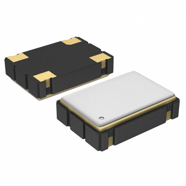
| 描述 | IC REG LDO 2.5V 1A 6WSON低压差稳压器 1A LDO W/Enable Pin |
| 产品分类 | |
| 品牌 | Texas Instruments |
| 产品手册 | http://www.ti.com/lit/gpn/lp38692 |
| 产品图片 |
|
| rohs | 符合RoHS无铅 / 符合限制有害物质指令(RoHS)规范要求 |
| 产品系列 | 电源管理 IC,低压差稳压器,Texas Instruments LP38692SD-2.5/NOPB- |
| 数据手册 | |
| 产品型号 | LP38692SD-2.5/NOPB |
| PSRR/纹波抑制—典型值 | 55 dB |
| 产品 | Low Dropout CMOS Linear Regulator |
| 产品目录页面 | |
| 产品种类 | 低压差稳压器 |
| 供应商器件封装 | 6-WSON (3x3) |
| 其它名称 | LP38692SD-2.5/NOPBDKR |
| 包装 | Digi-Reel® |
| 商标 | Texas Instruments |
| 回动电压—最大值 | 1.3 V |
| 安装类型 | 表面贴装 |
| 安装风格 | SMD/SMT |
| 封装 | Reel |
| 封装/外壳 | 6-WDFN 裸露焊盘 |
| 封装/箱体 | WSON-6 |
| 工作温度 | -40°C ~ 125°C |
| 工厂包装数量 | 1000 |
| 最大工作温度 | + 125 C |
| 最大输入电压 | 10 V |
| 最小工作温度 | - 40 C |
| 最小输入电压 | 2.7 V |
| 标准包装 | 1 |
| 电压-跌落(典型值) | 0.8V @ 1A |
| 电压-输入 | 最高 10V |
| 电压-输出 | 2.5V |
| 电流-输出 | 1A |
| 电流-限制(最小值) | - |
| 稳压器拓扑 | 正,固定式 |
| 稳压器数 | 1 |
| 类型 | Low Dropout Linear Regulator |
| 系列 | LP38692 |
| 设计资源 | http://www.digikey.com/product-highlights/cn/zh/texas-instruments-webench-design-center/3176 |
| 负载调节 | 1.8 % |
| 输出电压 | 2.5 V |
| 输出电流 | 1 A |
| 输出端数量 | 1 Output |
| 输出类型 | Fixed |
| 配用 | /product-detail/zh/LP38692EVAL/LP38692EVAL-ND/1640865 |


- 商务部:美国ITC正式对集成电路等产品启动337调查
- 曝三星4nm工艺存在良率问题 高通将骁龙8 Gen1或转产台积电
- 太阳诱电将投资9.5亿元在常州建新厂生产MLCC 预计2023年完工
- 英特尔发布欧洲新工厂建设计划 深化IDM 2.0 战略
- 台积电先进制程称霸业界 有大客户加持明年业绩稳了
- 达到5530亿美元!SIA预计今年全球半导体销售额将创下新高
- 英特尔拟将自动驾驶子公司Mobileye上市 估值或超500亿美元
- 三星加码芯片和SET,合并消费电子和移动部门,撤换高东真等 CEO
- 三星电子宣布重大人事变动 还合并消费电子和移动部门
- 海关总署:前11个月进口集成电路产品价值2.52万亿元 增长14.8%


PDF Datasheet 数据手册内容提取
Product Sample & Technical Tools & Support & Reference Folder Buy Documents Software Community Design LP38690,LP38692 SNVS322M–DECEMBER2004–REVISEDDECEMBER2015 LP38690, LP38692 1-A Low Dropout CMOS Linear Regulators Stable with Ceramic Output Capacitors 1 Features 3 Description • WideInputVoltageRange(2.7Vto10V) The LP38690 and LP38692 low-dropout CMOS linear 1 regulators provide tight output tolerance (2.5% • 2.5%OutputAccuracy(25°C) typical), extremely low dropout voltage (450 mV at a • LowDropoutVoltage:450mVat1A 1-A load current, V = 5 V), and excellent AC OUT (typical,5V ) performance utilizing ultra low ESR ceramic output OUT • Precision(Trimmed)BandgapReference capacitors. • EnsuredSpecificationsfor –40°Cto125°C The low thermal resistance of the WSON, SOT-223, and TO-252 packages allow the full operating current • 1-µAOff-StateQuiescentCurrent to be used even in high ambient temperature • ThermalOverloadProtection environments. • FoldbackCurrentLimiting The use of a PMOS power transistor means that no • 3-LeadTO-252,5-LeadSOT-223,and6-Bump DC base drive current is required to bias it allowing WSONPackages ground pin current to remain below 100 µA • EnablePin(LP38692) regardless of load current, input voltage, or operating temperature. • GroundPinCurrent:55µA(typical)atFullLoad • PrecisionOutputVoltage:2.5%(25°C)Accuracy DeviceInformation(1) PARTNUMBER PACKAGE BODYSIZE(NOM) 2 Applications TO-252(3) 6.58mmx6.10mm • HardDiskDrives LP38690 WSON(6) 3.00mmx3.00mm • NotebookComputers SOT-223(5) 6.50mmx3.56mm LP38692 • BatteryPoweredDevices WSON(6) 3.00mmx3.00mm • PortableInstrumentation (1) For all available packages, see the orderable addendum at theendofthedatasheet. SimplifiedSchematicforLP38690 SimplifiedSchematicforLP38692 VIN VOUT VIN VOUT IN OUT IN OUT LP38690 EN LP38692 SNS** VEN SNS** 1 µF* GND 1 µF* 1 PF * GND 1 PF * *Minimumvaluerequiredforstability. **WSONpackagedevicesonly. *Minimumvaluerequiredforstability. **WSONpackagedevicesonly. 1 An IMPORTANT NOTICE at the end of this data sheet addresses availability, warranty, changes, use in safety-critical applications, intellectualpropertymattersandotherimportantdisclaimers.PRODUCTIONDATA.
LP38690,LP38692 SNVS322M–DECEMBER2004–REVISEDDECEMBER2015 www.ti.com Table of Contents 1 Features.................................................................. 1 8.1 ApplicationInformation............................................14 2 Applications........................................................... 1 8.2 TypicalApplications................................................15 3 Description............................................................. 1 9 PowerSupplyRecommendations...................... 18 4 RevisionHistory..................................................... 2 10 Layout................................................................... 18 5 PinConfigurationandFunctions......................... 3 10.1 PCBLayout...........................................................18 10.2 LayoutExamples...................................................19 6 Specifications......................................................... 4 10.3 WSONMounting...................................................19 6.1 AbsoluteMaximumRatings......................................4 10.4 RFI/EMISusceptibility...........................................20 6.2 ESDRatings..............................................................4 10.5 OutputNoise.........................................................20 6.3 RecommendedOperatingConditions.......................4 11 DeviceandDocumentationSupport................. 21 6.4 ThermalInformation..................................................4 6.5 ElectricalCharacteristics...........................................5 11.1 DocumentationSupport .......................................21 6.6 TypicalCharacteristics..............................................6 11.2 RelatedLinks........................................................21 11.3 CommunityResources..........................................21 7 DetailedDescription............................................ 11 11.4 Trademarks...........................................................21 7.1 Overview.................................................................11 11.5 ElectrostaticDischargeCaution............................21 7.2 FunctionalBlockDiagrams.....................................11 11.6 Glossary................................................................21 7.3 FeatureDescription.................................................13 12 Mechanical,Packaging,andOrderable 7.4 DeviceFunctionalModes........................................13 Information........................................................... 21 8 ApplicationandImplementation........................ 14 4 Revision History NOTE:Pagenumbersforpreviousrevisionsmaydifferfrompagenumbersinthecurrentversion. ChangesfromRevisionL(March2015)toRevisionM Page • AddedtopnavigatoriconforTIDesigns ............................................................................................................................... 1 • AddedCautionnotetoFoldbackCurrentLimitingsubsection ............................................................................................ 13 ChangesfromRevisionK(December2014)toRevisionL Page • Changed"mA"backto"mV"-errorfromSDSconversion.................................................................................................... 5 ChangesfromRevisionJ(April2013)toRevisionK Page • ChangedDeviceInformationandESDRatingtables,FeatureDescription,DeviceFunctionalModes,Application andImplementation,PowerSupplyRecommendations,Layout,DeviceandDocumentationSupport,and Mechanical,Packaging,andOrderableInformationsections;updateThermalValuesmovedsomecurvesto ApplicationCurvessection;changepackagenamePFMtoTO-252(NationaltoTInomenclature)andpinnames fromVIN,VOUTtoIN,OUT. ................................................................................................................................................. 1 ChangesfromRevisionI(April2013)toRevisionJ Page • ChangedlayoutofNationalDataSheettoTIformat........................................................................................................... 20 2 SubmitDocumentationFeedback Copyright©2004–2015,TexasInstrumentsIncorporated ProductFolderLinks:LP38690 LP38692
LP38690,LP38692 www.ti.com SNVS322M–DECEMBER2004–REVISEDDECEMBER2015 5 Pin Configuration and Functions LP38690TO-252(NDP) LP38690WSON(NGG) 3Pins 6Pins TopView TopView IN 1 6 IN Exposed Pad GND 2 on Bottom 5 SNS (DAP) N/C 3 4 OUT LP38690/92SOT-223(NDC) LP38692WSON(NGG) 5Pins 6Pins TopView TopView EN1 IN 1 6 IN N/C2 5GND OUT3 Exposed Pad GND 2 on Bottom 5 SNS IN4 (DAP) EN 3 4 OUT PinFunctions PIN LP38690 LP38692 TYPE DESCRIPTION NAME TO-252 WSON SOT-223 WSON TheEnable(EN)pinallowstheparttobeturnedONandOFFbypullingthis EN — — 1 3 I pinHIGHorLOW. Circuitgroundfortheregulator.FortheTO-252andSOT-223packagesthis GND TAB 2 5 2 — isthermallyconnectedtothedieandfunctionsasaheatsinkwhensoldered downtoalargecopperplane. Thisistheinputsupplyvoltagetotheregulator.ForWSONdevices,bothIN IN 3 1,6 4 1,6 I pinsmustbetiedtogetherforfullcurrentoperation(500mAmaximumper pin). OUT 1 4 3 4 O Regulatedoutputvoltage. WSONonly-Outputsensepinallowsremotesensingattheloadwhich eliminatestheerrorinoutputvoltageduetovoltagedropscausedbythe SNS — 5 — 5 I resistanceinthetracesbetweentheregulatorandtheload.Thispinmust betiedtoVOUT. WSONonly-TheDAP(ExposedPad)functionsasathermalconnection DAP — X — X — whensolderedtoacopperplane.SeeWSONMountingsectioninLayoutfor moreinformation. Copyright©2004–2015,TexasInstrumentsIncorporated SubmitDocumentationFeedback 3 ProductFolderLinks:LP38690 LP38692
LP38690,LP38692 SNVS322M–DECEMBER2004–REVISEDDECEMBER2015 www.ti.com 6 Specifications 6.1 Absolute Maximum Ratings overoperatingfree-airtemperaturerange(unlessotherwisenoted)(1) MIN MAX UNIT V(max)Allpins(withrespecttoGND) –0.3 12 V I (2) Internallylimited OUT Junctiontemperature −40 150 °C Leadtemperature(soldering,5seconds) 260 Powerdissipation(3) Internallylimited Storagetemperature,T –65 150 °C stg (1) StressesbeyondthoselistedunderAbsoluteMaximumRatingsmaycausepermanentdamagetothedevice.Thesearestressratings only,whichdonotimplyfunctionaloperationofthedeviceattheseoranyotherconditionsbeyondthoseindicatedunderRecommended OperatingConditions.Exposuretoabsolute-maximum-ratedconditionsforextendedperiodsmayaffectdevicereliability. (2) Ifusedinadual-supplysystemwheretheregulatorloadisreturnedtoanegativesupply,theoutputpinmustbediodeclampedto ground. (3) Atelevatedtemperatures,devicepowerdissipationmustbederatedbasedonpackagethermalresistanceandheatsinkvalues(ifa heatsinkisused).WhenusingtheWSONpackage,refertoTIApplicationReportAN-1187LeadlessLeadframePackage(LLP) (SNOA401)andtheWSONMountingsectioninthisdatasheet.Ifpowerdissipationcausesthejunctiontemperaturetoexceedspecified limits,thedevicegoesintothermalshutdown. 6.2 ESD Ratings VALUE UNIT V Electrostaticdischarge Human-bodymodel(HBM),perANSI/ESDA/JEDECJS-001(1) ±2000 V (ESD) (1) JEDECdocumentJEP155statesthat500-VHBMallowssafemanufacturingwithastandardESDcontrolprocess. 6.3 Recommended Operating Conditions overoperatingfree-airtemperaturerange(unlessotherwisenoted) MIN NOM MAX UNIT V supplyvoltage 2.7 10 V IN Operatingjunctiontemperature −40 125 °C 6.4 Thermal Information LP38690 LP38690/92 LP38692 THERMALMETRIC(1) TO-252 WSON SOT-223 UNIT 3PINS 6PINS 5PINS R (2) Junction-to-ambientthermalresistance 50.5 50.6 68.5 °C/W θJA R Junction-to-case(top)thermalresistance 52.6 44.4 52.2 °C/W θJC(top) R Junction-to-boardthermalresistance 29.7 24.9 13.0 °C/W θJB ψ Junction-to-topcharacterizationparameter 4.8 0.4 5.5 °C/W JT ψ Junction-to-boardcharacterizationparameter 29.3 25.1 12.8 °C/W JB R Junction-to-case(bottom)thermalresistance 1.5 5.4 n/a °C/W θJC(bot) (1) Formoreinformationabouttraditionalandnewthermalmetrics,seetheSemiconductorandICPackageThermalMetricsapplication report,SPRA953. (2) Junction-to-ambientthermalresistance,High-K. 4 SubmitDocumentationFeedback Copyright©2004–2015,TexasInstrumentsIncorporated ProductFolderLinks:LP38690 LP38692
LP38690,LP38692 www.ti.com SNVS322M–DECEMBER2004–REVISEDDECEMBER2015 6.5 Electrical Characteristics Unlessotherwisespecified:V =V +1V,C =C =10µF,I =10mA,andlimitsareforT =25°C.Minimum(MIN) IN OUT IN OUT LOAD J andmaximum(MAX)limitsarespecifiedthroughtesting,statisticalcorrelation,ordesign. PARAMETER TESTCONDITIONS MIN TYP(1) MAX UNIT –2.5 2.5 VOUT Outputvoltagetolerance 100µA<IL<1A %VOUT V +1V≤V ≤10V –5 5 O IN −40°C≤T ≤125°C J V +0.5V≤V ≤10V OUT IN 0.03 I =25mA L Outputvoltageline ΔVOUT/ΔVIN regulation(2) VOUT+0.5V≤VIN≤10V %/A I =25mA 1 L −40°C≤T ≤125°C J 1mA<I <1A L 1.8 V =V +1V IN OUT Outputvoltageload ΔVOUT/ΔIL regulation(3) 1mA<IL<1A V V =V +1V 5 IN OUT −40°C≤T ≤125°C J V =1.8V OUT 950 I =1A L V =1.8V OUT I =1A 1600 L −40°C≤T ≤125°C J I =0.1A 80 L V =2.5V OUT I =1A 800 L V =2.5V I =0.1A 145 OUT L −40°C≤T ≤125°C J I =1A 1300 V –V Dropoutvoltage(4) L mV IN OUT I =0.1A 65 L V =3.3V OUT I =1A 650 L VOUT=3.3V IL=0.1A 110 −40°C≤TJ≤125°C IL=1A 1000 I =0.1A 45 L V =5V OUT I =1A 450 L V =5V, I =0.1A 100 OUT L −40°C≤T ≤125°C J I =1A 800 L V ≤10V,I =100µAto1A 55 IN L V ≤10V,I =100µAto1A I Quiescentcurrent IN L 100 Q −40°C≤T ≤125°C J µA V ≤0.4V(LP38692only) 0.001 EN V –V ≤4V I (MIN) Minimumloadcurrent IN OUT 100 L −40°C≤T ≤125°C J V –V >5V 450 IN OUT I Foldbackcurrentlimit mA FB V –V <4V 1500 IN OUT PSRR Ripplerejection V =V +2V ,with1V /120 IN OUT (DC) (p-p) 55 dB Hzripple T Thermalshutdown SD 160 activation(junctiontemp) °C T (HYST) Thermalshutdown SD 10 hysteresis(junctiontemp) e Outputnoise V =3.3V,BW=10Hzto10kHz 0.7 µV/√Hz n OUT V (LEAK) Outputleakagecurrent V =V +1Vat10V 0.5 12 µA OUT OUT OUT(NOM) IN (1) Typicalnumbersrepresentthemostlikelyparametricnormfor25°Coperation. (2) Outputvoltagelineregulationisdefinedasthechangeinoutputvoltagefromnominalvalueresultingfromachangeininputvoltage. (3) Outputvoltageloadregulationisdefinedasthechangeinoutputvoltagefromnominalvalueastheloadcurrentincreasesfrom1mAto fullload. (4) Dropoutvoltageisdefinedastheminimuminputtooutputdifferentialrequiredtomaintaintheoutputwithin100mVofnominalvalue. Copyright©2004–2015,TexasInstrumentsIncorporated SubmitDocumentationFeedback 5 ProductFolderLinks:LP38690 LP38692
LP38690,LP38692 SNVS322M–DECEMBER2004–REVISEDDECEMBER2015 www.ti.com Electrical Characteristics (continued) Unlessotherwisespecified:V =V +1V,C =C =10µF,I =10mA,andlimitsareforT =25°C.Minimum(MIN) IN OUT IN OUT LOAD J andmaximum(MAX)limitsarespecifiedthroughtesting,statisticalcorrelation,ordesign. PARAMETER TESTCONDITIONS MIN TYP(1) MAX UNIT Output=OFF,−40°C≤T ≤125°C 0.4 J Output=ON,V =4V 1.8 IN −40°C≤T ≤125°C J Enablevoltage(LP38692 VEN only) Output=ON,VIN=6V 3 V −40°C≤T ≤125°C J Output=ON,V =10V 4 IN −40°C≤T ≤125°C J I Enablepinleakage V =0Vor10V,V =10V –1 0.001 1 µA EN EN IN 6.6 Typical Characteristics Unlessotherwisespecified:T =25°C,C =C =10µF,ENpinistiedtoV (LP38692only),V =1.8V,V =V +1 J IN OUT IN OUT IN OUT V,I =10mA. L 1.2 1.0 COUT = 1 PF COUT = 10 PF 1.0 0.8 Hz) 0.8 Hz) 0.6 V V/ NOISE/ (P 00..46 NOISE (P 0.4 0.2 0.2 0.0 0.0 10 100 1k 10k 100k 10 100 1k 10k 100k FREQUENCY (Hz) FREQUENCY (Hz) Figure1.NoisevsFrequency Figure2.NoisevsFrequency 1.5 60 COUT = 100 PF 50 Hz) 1.0 N (dB) 40 O V/ TI E (P EJEC 30 NOIS 0.5 PPLE R 20 COUT = 10 PF RI VIN(DC) = 5.3V 10 VIN(AC) = 1V(p-p) VOUT = 3.3V 0.0 0 10 100 1k 10k 100k 10 100 1k 10k 100k FREQUENCY (Hz) FREQUENCY (Hz) Figure3.NoisevsFrequency Figure4.RippleRejection 6 SubmitDocumentationFeedback Copyright©2004–2015,TexasInstrumentsIncorporated ProductFolderLinks:LP38690 LP38692
LP38690,LP38692 www.ti.com SNVS322M–DECEMBER2004–REVISEDDECEMBER2015 Typical Characteristics (continued) Unlessotherwisespecified:T =25°C,C =C =10µF,ENpinistiedtoV (LP38692only),V =1.8V,V =V +1 J IN OUT IN OUT IN OUT V,I =10mA. L 60 60 50 50 B) B) N (d 40 N (d 40 O O CTI CTI E 30 E 30 EJ EJ RIPPLE R 1200 CVVIIONNU((DATC C=)) 1==0 150V. 3P(VFp-p) RIPPLE R 1200 CVVVIIOONNUU((DATT C C==)) 3 1==. 3 P15VFV.3(Vp-p) VOUT = 3.3V 0 0 10 100 1k 10k 100k 10 100 1k 10k 100k FREQUENCY (Hz) FREQUENCY (Hz) Figure5.RippleRejection Figure6.RippleRejection VOUT = 3.3V VOUT = 3.3V 20 COUT = 100 PF 100 COUT = 10 PF V) 10 VOUT V) 50 m m VOUT (T 0 (T 0 U U O O V’ -10 V’ -50 -20 -100 5 5 VIN V) VIN V) 4 (N 4 (N VI VI 3 3 200 P s/DIV 100 P s/DIV Figure7.LineTransientResponse Figure8.LineTransientResponse 100 VOUT = 3.3V 100 COUT = 1 PF mV) 50 V) 50 (T 0 VOUT m VOUT OU (UT 0 V’ -50 COUT = 100 PF O V’ -50 -100 -100 1 ILOAD A) 5 (D VIN V) OA 4 (N 0.01 IL VI 3 100 P s/DIV 200 P s/DIV Figure9.LineTransientResponse Figure10.LoadTransientResponse Copyright©2004–2015,TexasInstrumentsIncorporated SubmitDocumentationFeedback 7 ProductFolderLinks:LP38690 LP38692
LP38690,LP38692 SNVS322M–DECEMBER2004–REVISEDDECEMBER2015 www.ti.com Typical Characteristics (continued) Unlessotherwisespecified:T =25°C,C =C =10µF,ENpinistiedtoV (LP38692only),V =1.8V,V =V +1 J IN OUT IN OUT IN OUT V,I =10mA. L 400 200 V) 200 COUT = 10 PF V) 100 COUT = 10 PF m m (OUT 0 VOUT (OUT 0 VOUT V’ -200 V’ -100 -400 -200 0.5 1 ILOAD (A)AD ILOAD (A)OAD O L 0.01 IL 0.01 I 40 Ps /DIV 40 Ps /DIV Figure11.LoadTransientResponse Figure12.LoadTransientResponse 400 400 COUT = 1 PF COUT = 1 PF V) 200 V) 200 m VOUT m (T 0 (T 0 U U O O VOUT V -200 V -200 ’ ’ -400 -400 0.5 1 ILOAD (A)D ILOAD (A)AD A O O L 0.01 IL 0.01 I 10 Ps /DIV 10 Ps /DIV Figure13.LoadTransientResponse Figure14.LoadTransientResponse 0.4 0.4 0.2 0.2 0 0 NOITAIV --00..42 EVIATION --00..42 E D D % -0.6 % -0.6 -0.8 -0.8 -1 -1 -1.2 -50 -25 0 25 50 75 100 125 -50 -25 0 25 50 75 100 125 TEMPERATURE (oC) TEMPERATURE (oC) Figure15.VOUTvsTemperature(5V) Figure16. VOUTvsTemperature(3.3V) 8 SubmitDocumentationFeedback Copyright©2004–2015,TexasInstrumentsIncorporated ProductFolderLinks:LP38690 LP38692
LP38690,LP38692 www.ti.com SNVS322M–DECEMBER2004–REVISEDDECEMBER2015 Typical Characteristics (continued) Unlessotherwisespecified:T =25°C,C =C =10µF,ENpinistiedtoV (LP38692only),V =1.8V,V =V +1 J IN OUT IN OUT IN OUT V,I =10mA. L 0.1 0.2 0 0.1 0 -0.1 NOITAIVED % ---000...432 NOITAIVED % ----0000....4321 -0.5 -0.5 -0.6 -0.6 -0.7 -0.7 -50 -25 0 25 50 75 100 125 -50 -25 0 25 50 75 100 125 TEMPERATURE (oC) TEMPERATURE (oC) Figure17. V vsTemperature(2.5V) Figure18. V vsTemperature(1.8V) OUT OUT Figure20.V vsV (Power-Up) Figure19.V vsV (1.8V) OUT IN OUT IN 1600 1000 1400 125°C 900 VOUT = 3.3V 800 1200 700 (mV)UT 1800000 )Vm( TUO 560000 125°C O P ROP 600 -40°C 25°C ORD 400 VD V 300 400 -40°C 25°C 200 200 100 0 0 0 200 400 600 800 1000 0 200 400 600 800 1000 IOUT (mA) IOUT (mA) Figure22.DropoutVoltagevsI Figure21.DropoutVoltagevsI OUT OUT Copyright©2004–2015,TexasInstrumentsIncorporated SubmitDocumentationFeedback 9 ProductFolderLinks:LP38690 LP38692
LP38690,LP38692 SNVS322M–DECEMBER2004–REVISEDDECEMBER2015 www.ti.com Typical Characteristics (continued) Unlessotherwisespecified:T =25°C,C =C =10µF,ENpinistiedtoV (LP38692only),V =1.8V,V =V +1 J IN OUT IN OUT IN OUT V,I =10mA. L 2.3 -1.0 2.1 VIN = 10V -1.5 1.9 1.7 %/A) (V)N 1.5 VIN = 6V (OUT -2.0 VE 1.3 ’/IT -2.5 U 1.1 O V ’ 0.9 VIN = 4V -3.0 0.7 0.5 -3.5 -50 -25 0 25 50 75 100 125 -50 -25 0 25 50 75 100 125 TEMPERATURE (oC) TEMPERATURE (oC) Figure23.EnableVoltagevsTemperature Figure24.LoadRegulationvsTemperature 0.034 0.032 0.03 V) %/ (N 0.028 VI ’ /T 0.026 U O V ’ 0.024 0.022 0.02 -50 -25 0 25 50 75 100 125 TEMPERATURE (oC) Figure25.LineRegulationvsTemperature 10 SubmitDocumentationFeedback Copyright©2004–2015,TexasInstrumentsIncorporated ProductFolderLinks:LP38690 LP38692
LP38690,LP38692 www.ti.com SNVS322M–DECEMBER2004–REVISEDDECEMBER2015 7 Detailed Description 7.1 Overview The LP38690 and LP38692 devices are designed to meet the requirements of portable, battery-powered digital systems providing an accurate output voltage with fast start-up. When disabled via a low logic signal at the enable pin (EN), the power consumption is reduced to virtually zero (LP38692 only). The LP38690 and LP38692 performwellwithasingle1-μFinputcapacitorandasingle1-μFceramicoutputcapacitor. 7.2 Functional Block Diagrams IN P-FET - P-FET MOSFET DRIVER + ENABLE LOGIC FOLDBACK CURRENT OUT LIMITING R THERMAL 1.25V SHUTDOWN REFERENCE 1 R 2 GND Figure26. LP38690FunctionalDiagram(TO-252) IN P-FET - P-FET MOSFET DRIVER + ENABLE N/C LOGIC FOLDBACK CURRENT OUT LIMITING SNS THERMAL 1.25 V SHUTDOWN REFERENCE R1 R2 GND Figure27. LP38690FunctionalDiagram(WSON) Copyright©2004–2015,TexasInstrumentsIncorporated SubmitDocumentationFeedback 11 ProductFolderLinks:LP38690 LP38692
LP38690,LP38692 SNVS322M–DECEMBER2004–REVISEDDECEMBER2015 www.ti.com Functional Block Diagrams (continued) IN P-FET - P-FET MOSFET DRIVER + ENABLE EN LOGIC FOLDBACK CURRENT OUT LIMITING THERMAL 1.25V SHUTDOWN REFERENCE R1 R2 GND Figure28. LP38692FunctionalDiagram(SOT-223) IN P-FET - P-FET MOSFET DRIVER + ENABLE EN LOGIC FOLDBACK CURRENT OUT LIMITING SNS R THERMAL 1.25V SHUTDOWN REFERENCE 1 R 2 GND Figure29. LP38692FunctionalDiagram(WSON) 12 SubmitDocumentationFeedback Copyright©2004–2015,TexasInstrumentsIncorporated ProductFolderLinks:LP38690 LP38692
LP38690,LP38692 www.ti.com SNVS322M–DECEMBER2004–REVISEDDECEMBER2015 7.3 Feature Description 7.3.1 Enable(EN) The LP38692 has an Enable pin (EN) which allows an external control signal to turn the regulator output On and Off. The Enable On/Off threshold has no hysteresis. The voltage signal must rise and fall cleanly, and promptly, through the ON and OFF voltage thresholds. The EN pin voltage must be higher than the V threshold to EN(MIN) ensure that the device is fully enabled under all operating conditions. The EN pin voltage must be lower than the V threshold to ensure that the device is fully disabled. The Enable pin has no internal pull-up or pull-down EN(MAX) to establish a default condition and, as a result, this pin must be terminated either actively or passively. If the Enable pin is driven from a source that actively pulls high and low, the drive voltage should not be allowed to go below ground potential or higher than V . If the application does not require the Enable function, the pin should IN beconnecteddirectlytotheINpin. 7.3.2 ThermalShutdownProtection(TSD) Thermal shutdown disables the output when the junction temperature rises to approximately 160°C which allows thedevicetocool.Whenthejunctiontemperaturecoolstoapproximately150°C,theoutputcircuitryenables. Based on power dissipation, thermal resistance, and ambient temperature, the thermal protection circuit may cycle on and off. This thermal cycling limits the dissipation of the regulator and protects it from damage as a resultofoverheating. The TSD circuitry of the LP38692 has been designed to protect against temporary thermal overload conditions. TheTSDcircuitrywasnotintendedtoreplaceproperheat-sinking.ContinuouslyrunningtheLP38692deviceinto thermalshutdowndegradesdevicereliability. 7.3.3 FoldbackCurrentLimiting Foldback current limiting is built into the LP38690 and LP38692 which reduces the amount of output current the part can deliver as the output voltage is reduced. The amount of load current is dependent on the differential voltage between V and V . Typically, when this differential voltage exceeds 5 V, the load current limits at IN OUT about450mA.WhentheV –V differentialisreducedbelow4V,loadcurrentislimitedtoabout1500mA. IN OUT CAUTION When toggling the LP38692 Enable (EN) after the input voltage (V ) is applied, the IN foldback current limit circuitry is functional the first time that the EN pin is taken high. The foldback current limit circuitry is non-functional the second, and subsequent, times that the EN pin is taken high. Depending on the input and output capacitance values the input inrush current may be higher than expected which can cause the input voltagetodroop. If the EN pin is connected to the IN pin, the foldback current limit circuitry is functional whenV isappliedifV startsfromlessthan0.4V. IN IN 7.4 Device Functional Modes 7.4.1 Enable(EN) The EN pin voltage must be higher than the V threshold to ensure that the device is fully enabled under all EN(MIN) operatingconditions. 7.4.2 MinimumOperatingInputVoltage(V ) IN The LP38690 and LP38692 devices do not include any dedicated UVLO circuitry. The LP38690 and LP38692 internal circuitry is not fully functional until V is at least 2.7 V. The output voltage is not regulated until V ≥ IN IN (V +V ),or2.7V,whicheverishigher. OUT DO Copyright©2004–2015,TexasInstrumentsIncorporated SubmitDocumentationFeedback 13 ProductFolderLinks:LP38690 LP38692
LP38690,LP38692 SNVS322M–DECEMBER2004–REVISEDDECEMBER2015 www.ti.com 8 Application and Implementation NOTE Information in the following applications sections is not part of the TI component specification, and TI does not warrant its accuracy or completeness. TI’s customers are responsible for determining suitability of components for their purposes. Customers should validateandtesttheirdesignimplementationtoconfirmsystemfunctionality. 8.1 Application Information 8.1.1 ReverseVoltage A reverse voltage condition exists when the voltage at the output pin is higher than the voltage at the input pin. Typically this happens when V is abruptly taken low and C continues to hold a sufficient charge such that IN OUT the input to output voltage becomes reversed. A less common condition is when an alternate voltage source is connectedtotheoutput. There are two possible paths for current to flow from the output pin back to the input during a reverse voltage condition. 1. While V is high enough to keep the control circuitry alive, and the EN pin (LP38692 only) is above the IN V threshold, the control circuitry attempts to regulate the output voltage. If the input voltage is less than EN(ON) the programmed output voltage, the control circuit drives the gate of the pass element to the full ON condition. In this condition, reverse current flows from the output pin to the input pin, limited only by the R of the pass element and the output to input voltage differential. Discharging an output capacitor up to DS(ON) 1000 μF in this manner does not damage the device as the current will rapidly decay. However, continuous reversecurrentshouldbeavoided.WhentheENpinislowthisconditionisprevented. 2. The internal PFET pass element has an inherent parasitic diode. During normal operation, the input voltage is higher than the output voltage and the parasitic diode is reverse biased. However, when V is below the IN value where the control circuitry is alive, or the EN pin is low (LP38692 only), and the output voltage is more than 500 mV (typical) above the input voltage the parasitic diode becomes forward biased and current flows from the output pin to the input pin through the diode. The current in the parasitic diode should be limited to lessthan1Acontinuousand5Apeak. If used in a dual-supply system where the regulator output load is returned to a negative supply, the output pin must be diode clamped to ground to limit the negative voltage transition. A Schottky diode is recommendedforthisprotectiveclamp. 14 SubmitDocumentationFeedback Copyright©2004–2015,TexasInstrumentsIncorporated ProductFolderLinks:LP38690 LP38692
LP38690,LP38692 www.ti.com SNVS322M–DECEMBER2004–REVISEDDECEMBER2015 8.2 Typical Applications VIN VOUT IN OUT LP38690 SNS** 1 µF* GND 1 µF* *Minimumvaluerequiredforstability. **WSONpackagedevicesonly. Figure30. LP38690TypicalApplication VIN VOUT IN OUT EN LP38692 VEN SNS** 1 PF * GND 1 PF * *Minimumvaluerequiredforstability. **WSONpackagedevicesonly. Figure31. LP38692TypicalApplication 8.2.1 DesignRequirements FortypicalCMOSvoltageregulatorapplications,usetheparameterslistedinTable1. Table1.DesignParameters DESIGNPARAMETER EXAMPLEVALUE Inputvoltagerange 2.7to10V Outputvoltage 1.8V Outputcurrent 1A Outputcapacitorrange 1µF Input/outputcapacitorESRrange 5mΩto500mΩ Copyright©2004–2015,TexasInstrumentsIncorporated SubmitDocumentationFeedback 15 ProductFolderLinks:LP38690 LP38692
LP38690,LP38692 SNVS322M–DECEMBER2004–REVISEDDECEMBER2015 www.ti.com 8.2.2 DetailedDesignProcedure 8.2.2.1 PowerDissipationandDeviceOperation The permissible power dissipation for any package is a measure of the capability of the device to pass heat from the power source, the junctions of the device, to the ultimate heat sink, the ambient environment. Thus, the power dissipation is dependent on the ambient temperature and the thermal resistance across the various interfacesbetweenthediejunctionandambientair. The permissible power dissipation for any package is a measure of the capability of the device to pass heat from the power source, the junctions of the device, to the ultimate heat sink, the ambient environment. Thus, the power dissipation is dependent on the ambient temperature and the thermal resistance across the various interfacesbetweenthediejunctionandambientair. ThemaximumallowablepowerdissipationforthedeviceinagivenpackagecanbecalculatedusingEquation1: P =((T –T )/R ) (1) D-MAX J-MAX A θJA TheactualpowerbeingdissipatedinthedevicecanberepresentedbyEquation2: P =(V –V )×I (2) D IN OUT OUT These two equations establish the relationship between the maximum power dissipation allowed due to thermal consideration, the voltage drop across the device, and the continuous current capability of the device. These two equationsshouldbeusedtodeterminetheoptimumoperatingconditionsforthedeviceintheapplication. In applications where lower power dissipation (P ) and/or excellent package thermal resistance (R ) is present, D θJA themaximumambienttemperature(T )maybeincreased. A-MAX In applications where high power dissipation and/or poor package thermal resistance is present, the maximum ambient temperature (T ) may have to be derated. T is dependent on the maximum operating junction A-MAX A-MAX temperature (T = 125°C), the maximum allowable power dissipation in the device package in the J-MAX-OP application (P ), and the junction-to ambient thermal resistance of the part/package in the application (R ), D-MAX θJA asgivenbyEquation3: T =(T –(R ×P )) (3) A-MAX J-MAX-OP θJA D-MAX Alternately, if T can not be derated, the P value must be reduced. This can be accomplished by reducing A-MAX D V in the V – V term as long as the minimum V is met, or by reducing the I term, or by some IN IN OUT IN OUT combinationofthetwo. 8.2.2.2 ExternalCapacitors In common with most regulators, the LP38690 and LP38692 require external capacitors for regulator stability. The LP38690 and LP38692 are specifically designed for portable applications requiring minimum board space andsmallestcomponents.Thesecapacitorsmustbecorrectlyselectedforgoodperformance. 8.2.2.2.1 InputCapacitor An input capacitor is required for stability. It is recommended that a 1-μF capacitor be connected between the LP38690 or LP38692 IN pin and GND pin (this capacitance value may be increased without limit). This capacitor must be located a distance of not more than 1 cm from the IN pin and returned to a clean analogue ground. Any goodqualityceramic,tantalum,orfilmcapacitormaybeusedattheinput. Important: To ensure stable operation it is essential that good PCB design practices are employed to minimize ground impedance and keep input inductance low. If these conditions cannot be met, or if long leads are used to connect the battery or other power source to the LP38690 or LP38692, then it is recommended that the input capacitor is increased. Also, tantalum capacitors can suffer catastrophic failures due to surge current when connectedtoalow-impedancesourceofpower(likeabatteryoraverylargecapacitor).Ifatantalumcapacitoris used at the input, it must be ensured by the manufacturer to have a surge current rating sufficient for the application. There are no requirements for the equivalent series resistance (ESR) on the input capacitor, but tolerance and temperature coefficient must be considered when selecting the capacitor to ensure the capacitance remains approximately1 μFovertheentireoperatingtemperaturerange. 16 SubmitDocumentationFeedback Copyright©2004–2015,TexasInstrumentsIncorporated ProductFolderLinks:LP38690 LP38692
LP38690,LP38692 www.ti.com SNVS322M–DECEMBER2004–REVISEDDECEMBER2015 8.2.2.2.2 OutputCapacitor The LP38690 and LP38692 are designed specifically to work with very small ceramic output capacitors. A 1-μF ceramic capacitor (temperature types Z5U, Y5V or X7R/X5R) with ESR between 5 mΩ to 500 mΩ, is suitable in theLP38690orLP38692applicationcircuit. For this device the output capacitor should be connected between the OUT pin and GND pin. It is also possible tousetantalumorfilmcapacitorsatthedeviceoutput,butthesearenotasattractiveforreasonsofsizeandcost (see Capacitor Characteristics). The output capacitor must meet the requirement for the minimum value of capacitanceandalsohaveanESRvaluethatiswithintherange5mΩ to500mΩ forstability. 8.2.2.2.3 NoLoadStability The LP38690 and LP38692 remain stable and in regulation with no external load. This is an important considerationinsomecircuits,forexampleCMOSRAMkeep-aliveapplications. 8.2.2.2.4 CapacitorCharacteristics The LP38690 and LP38692 are designed to work with ceramic capacitors on the output to take advantage of the benefitstheyoffer.Forcapacitancevaluesintherangeof0.47 μFto4.7 μF,ceramiccapacitorsarethesmallest, least expensive and have the lowest ESR values, thus making them best for eliminating high frequency noise. The ESR of a typical 1-μF ceramic capacitor is in the range of 20 mΩ to 40 mΩ, which easily meets the ESR requirementforstabilityfortheLP38690orLP38692. For both input and output capacitors, careful interpretation of the capacitor specification is required to ensure correct device operation. The capacitor value can change greatly, depending on the operating conditions and capacitortype. Inparticular,theoutputcapacitorselectionshouldtakeaccountofallthecapacitorparameters,toensurethatthe specification is met within the application. The capacitance can vary with DC bias conditions as well as temperature and frequency of operation. Capacitor values also shows some decrease over time due to aging. The capacitor parameters are also dependent on the particular case size, with smaller sizes giving poorer performance figures in general. As an example, Figure 32 shows a typical graph comparing different capacitor case sizes in a capacitance vs DC bias plot. As shown in Figure 32, increasing the DC Bias condition can result in the capacitance value falling below the minimum value given in the recommended capacitor specifications table (0.7 μF in this case). Note that the graph shows the capacitance out of spec for the 0402 case size capacitorathigherbiasvoltages.Itisthereforerecommendedthatthecapacitormanufacturers’specificationsfor thenominalvaluecapacitorareconsultedforallconditions,assomecapacitorsizes(forexample,0402)maynot besuitableintheactualapplication. )F 0603, 10V, X5R P 1 100% L A N IM O 80% N fo % ( E 60% U L 0402, 6.3V, X5R A V P 40% A C 20% 0 1.0 2.0 3.0 4.0 5.0 DC BIAS (V) Figure32. TypicalVariationInCapacitancevsDCBias The ceramic capacitor’s value varies with temperature. The capacitor type X7R, which operates over a temperature range of –55°C to 125°C, only varies the capacitance to within ±15%. The capacitor type X5R has a similar tolerance over a reduced temperature range of –55°C to 85°C. Many large value ceramic capacitors, larger than 1 μF are manufactured with Z5U or Y5V temperature characteristics. Their capacitance can drop by more than 50% as the temperature varies from 25°C to 85°C. Therefore, X7R and X5R types are recommended overZ5UandY5Vinapplicationswheretheambienttemperaturechangessignificantlyaboveorbelow25°C. Copyright©2004–2015,TexasInstrumentsIncorporated SubmitDocumentationFeedback 17 ProductFolderLinks:LP38690 LP38692
LP38690,LP38692 SNVS322M–DECEMBER2004–REVISEDDECEMBER2015 www.ti.com Tantalum capacitors are less desirable than ceramic for use as output capacitors because they are more costly when comparing equivalent capacitance and voltage ratings in the 0.47-μF to 4.7-μF range. Another important consideration is that tantalum capacitors have higher ESR values than equivalent size ceramic capacitors. This means that while it may be possible to find a tantalum capacitor with an ESR value within the stable range, it would have to be larger in capacitance (which means bigger and more costly) than a ceramic capacitor with the same ESR value. It should also be noted that the ESR of a typical tantalum increases about 2:1 as the temperaturegoesfrom25°Cdownto-40°C,sosomeguardbandmustbeallowed. 8.2.3 ApplicationCurves Figure33.VOUTvsVEN,On(LP38692Only) Figure34.VOUTvsVEN,Off(LP38692Only) 9 Power Supply Recommendations The LP38690 and LP38692 are designed to operate from an input supply voltage range of 2.7 V to 10 V. The input supply must be well regulated and free of spurious noise. To ensure that the LP38690 or LP38692 output voltage is well regulated, the input supply must be at least V + 0.5 V, or 2.7 V, whichever is higher. A OUT minimumcapacitorvalueof1-μFisrequiredtobewithin1cmoftheINpin. 10 Layout 10.1 PCB Layout The dynamic performance of the LP38690 and LP38692 devices is dependent on the layout of the PCB. PCB layout practices that are adequate for typical LDOs may degrade the load regulation, PSRR, noise, or transient performanceoftheLP38690orLP38692. Best performance is achieved by placing C and C on the same side of the PCB as the LP38690 or IN OUT LP38692, and as close to the package as is practical. The ground connections for C and C must be back to IN OUT theLP38690orLP38692GNDpinusingaswideandshortacoppertraceasispractical. Connections using long trace lengths, narrow trace widths, or connections through vias must be avoided. These addparasiticinductancesandresistancethatresultininferiorperformanceespeciallyduringtransientconditions. A ground plane, either on the opposite side of a two-layer PCB, or embedded in a multi-layer PCB, is strongly recommended.Thisgroundplaneservestwopurposes: 1. Providesacircuitreferenceplanetoassureaccuracy,and 2. provides a thermal plane to remove heat from the LP38690 or LP38692 WSON package through thermal viasunderthepackageDAP. 18 SubmitDocumentationFeedback Copyright©2004–2015,TexasInstrumentsIncorporated ProductFolderLinks:LP38690 LP38692
LP38690,LP38692 www.ti.com SNVS322M–DECEMBER2004–REVISEDDECEMBER2015 10.2 Layout Examples C OUT Power Ground EN V OUT C OUT NC OUT GND V OUT OUT D IN N Power G Ground V IN VIN IN CIN C IN Figure35.LP38690TO-252Package Figure36.LP38692SOT-223Package V IN CIN IN 1 6 IN CIN IN 1 6 IN Power 2 Thermal 5 SNS Power 2 Thermal 5 SNS Ground Pad Ground Pad N/C 3 4 OUT EN 3 4 OUT C C OUT OUT Figure37.LP38690WSONPackage Figure38.LP38692WSONPackage 10.3 WSON Mounting The NGG0006A (No Pullback) 6-Lead WSON package requires specific mounting techniques which are detailed in the TI Application Report AN-1187 Leadless Leadframe Package (LLP) (SNOA401). Referring to the section PCB Design Recommendations (Page 5), it should be noted that the pad style which should be used with the WSON package is the NSMD (non-solder mask defined) type. Additionally, it is recommended the PCB terminal padstobe0.2mmlongerthanthepackagepadstocreateasolderfillettoimprovereliabilityandinspection. The input current is split between two IN pins, 1 and 6. The two IN pins must be connected together to ensure thatthedevicecanmeetallspecificationsattheratedcurrent. The thermal dissipation of the WSON package is directly related to the printed circuit board construction and the amountofadditionalcopperareaconnectedtotheDAP. TheDAP(exposedpad)onthebottomoftheWSONpackageisconnectedtothediesubstratewithaconductive dieattachadhesive.TheDAPhasnodirectelectrical(wire)connectiontoanyofthepins.ThereisaparasiticPN junction between the die substrate and the device ground. As such, it is strongly recommend that the DAP be connected directly to the ground at device lead 2 (such as GND). Alternately, but not recommended, the DAP maybeleftfloating(thatis,noelectricalconnection).TheDAPmustnotbeconnectedtoanypotentialotherthan ground. Copyright©2004–2015,TexasInstrumentsIncorporated SubmitDocumentationFeedback 19 ProductFolderLinks:LP38690 LP38692
LP38690,LP38692 SNVS322M–DECEMBER2004–REVISEDDECEMBER2015 www.ti.com 10.4 RFI/EMI Susceptibility Radio frequency interference (RFI) and electromagnetic interference (EMI) can degrade any integrated circuit’s performance because of the small dimensions of the geometries inside the device. In applications where circuit sources are present which generate signals with significant high frequency energy content (> 1 MHz), care must betakentoensurethatthisdoesnotaffectthedeviceregulator. If RFI/EMI noise is present on the input side of the regulator (such as applications where the input source comes from the output of a switching regulator), good ceramic bypass capacitors must be used at the IN pin of the device. If a load is connected to the device output which switches at high speed (such as a clock), the high-frequency currentpulsesrequiredbytheloadmustbesuppliedbythecapacitorsonthedeviceoutput.Sincethebandwidth of the regulator loop is less than 100 kHz, the control circuitry cannot respond to load changes above that frequency. This means the effective output impedance of the device at frequencies above 100 kHz is determined onlybytheoutputcapacitors. In applications where the load is switching at high speed, the output of the device may need RF isolation from the load. It is recommended that some inductance be placed between the output capacitor and the load, and goodRFbypasscapacitorsbeplaceddirectlyacrosstheload. PCB layout is also critical in high noise environments, since RFI/EMI is easily radiated directly into PC traces. Noisy circuitry should be isolated from clean circuits where possible, and grounded through a separate path. At MHz frequencies, ground planes begin to look inductive and RFI/ EMI can cause ground bounce across the ground plane. In multi-layer PCB applications, care should be taken in layout so that noisy power and ground planesdonotradiatedirectlyintoadjacentlayerswhichcarryanalogpowerandground. 10.5 Output Noise Noise is specified in two ways: Spot Noise or Output Noise Density is the RMS sum of all noise sources, measuredattheregulatoroutput,ataspecificfrequency(measuredwitha1-Hzbandwidth).Thistypeofnoiseis usually plotted on a curve as a function of frequency. Total Output Noise or Broad-Band Noise is the RMS sum ofspotnoiseoveraspecifiedbandwidth,usuallyseveraldecadesoffrequencies. Attention should be paid to the units of measurement. Spot noise is measured in units µV/√Hz or nV/√Hz and totaloutputnoiseismeasuredinµV RMS The primary source of noise in low-dropout regulators is the internal reference. Noise can be reduced in two ways: by increasing the transistor area or by increasing the current drawn by the internal reference. Increasing the area decreases the chance of fitting the die into a smaller package. Increasing the current drawn by the internalreferenceincreasesthetotalsupplycurrent(GNDpincurrent). 20 SubmitDocumentationFeedback Copyright©2004–2015,TexasInstrumentsIncorporated ProductFolderLinks:LP38690 LP38692
LP38690,LP38692 www.ti.com SNVS322M–DECEMBER2004–REVISEDDECEMBER2015 11 Device and Documentation Support 11.1 Documentation Support 11.1.1 RelatedDocumentation Forrelateddocumentation,seethefollowing: TIApplicationReportAN-1187LeadlessLeadframePackage(LLP)(SNOA401) 11.2 Related Links Table 2 below lists quick access links. Categories include technical documents, support and community resources,toolsandsoftware,andquickaccesstosampleorbuy. Table2.RelatedLinks TECHNICAL TOOLS& SUPPORT& PARTS PRODUCTFOLDER SAMPLE&BUY DOCUMENTS SOFTWARE COMMUNITY LP38690 Clickhere Clickhere Clickhere Clickhere Clickhere LP38692 Clickhere Clickhere Clickhere Clickhere Clickhere 11.3 Community Resources The following links connect to TI community resources. Linked contents are provided "AS IS" by the respective contributors. They do not constitute TI specifications and do not necessarily reflect TI's views; see TI's Terms of Use. TIE2E™OnlineCommunity TI'sEngineer-to-Engineer(E2E)Community.Createdtofostercollaboration amongengineers.Ate2e.ti.com,youcanaskquestions,shareknowledge,exploreideasandhelp solveproblemswithfellowengineers. DesignSupport TI'sDesignSupport QuicklyfindhelpfulE2Eforumsalongwithdesignsupporttoolsand contactinformationfortechnicalsupport. 11.4 Trademarks E2EisatrademarkofTexasInstruments. Allothertrademarksarethepropertyoftheirrespectiveowners. 11.5 Electrostatic Discharge Caution Thesedeviceshavelimitedbuilt-inESDprotection.Theleadsshouldbeshortedtogetherorthedeviceplacedinconductivefoam duringstorageorhandlingtopreventelectrostaticdamagetotheMOSgates. 11.6 Glossary SLYZ022—TIGlossary. Thisglossarylistsandexplainsterms,acronyms,anddefinitions. 12 Mechanical, Packaging, and Orderable Information The following pages include mechanical, packaging, and orderable information. This information is the most current data available for the designated devices. This data is subject to change without notice and revision of thisdocument.Forbrowser-basedversionsofthisdatasheet,refertotheleft-handnavigation. Copyright©2004–2015,TexasInstrumentsIncorporated SubmitDocumentationFeedback 21 ProductFolderLinks:LP38690 LP38692
PACKAGE OPTION ADDENDUM www.ti.com 6-Feb-2020 PACKAGING INFORMATION Orderable Device Status Package Type Package Pins Package Eco Plan Lead/Ball Finish MSL Peak Temp Op Temp (°C) Device Marking Samples (1) Drawing Qty (2) (6) (3) (4/5) LP38690DT-1.8/NOPB ACTIVE TO-252 NDP 3 75 Green (RoHS SN Level-2-260C-1 YEAR -40 to 125 LP38690 & no Sb/Br) DT-1.8 LP38690DT-2.5/NOPB ACTIVE TO-252 NDP 3 75 Green (RoHS SN Level-2-260C-1 YEAR -40 to 125 LP38690 & no Sb/Br) DT-2.5 LP38690DT-3.3 NRND TO-252 NDP 3 75 TBD Call TI Call TI -40 to 125 LP38690 DT-3.3 LP38690DT-3.3/NOPB ACTIVE TO-252 NDP 3 75 Green (RoHS SN Level-2-260C-1 YEAR -40 to 125 LP38690 & no Sb/Br) DT-3.3 LP38690DT-5.0/NOPB ACTIVE TO-252 NDP 3 75 Green (RoHS SN Level-2-260C-1 YEAR -40 to 125 LP38690 & no Sb/Br) DT-5.0 LP38690DTX-1.8/NOPB ACTIVE TO-252 NDP 3 2500 Green (RoHS SN Level-2-260C-1 YEAR -40 to 125 LP38690 & no Sb/Br) DT-1.8 LP38690DTX-2.5/NOPB ACTIVE TO-252 NDP 3 2500 Green (RoHS SN Level-2-260C-1 YEAR -40 to 125 LP38690 & no Sb/Br) DT-2.5 LP38690DTX-3.3/NOPB ACTIVE TO-252 NDP 3 2500 Green (RoHS SN Level-2-260C-1 YEAR -40 to 125 LP38690 & no Sb/Br) DT-3.3 LP38690DTX-5.0/NOPB ACTIVE TO-252 NDP 3 2500 Green (RoHS SN Level-2-260C-1 YEAR -40 to 125 LP38690 & no Sb/Br) DT-5.0 LP38690SD-1.8 NRND WSON NGG 6 1000 TBD Call TI Call TI -40 to 125 L113B LP38690SD-1.8/NOPB ACTIVE WSON NGG 6 1000 Green (RoHS NIPDAU | SN Level-1-260C-UNLIM -40 to 125 L113B & no Sb/Br) LP38690SD-2.5/NOPB ACTIVE WSON NGG 6 1000 Green (RoHS SN Level-1-260C-UNLIM -40 to 125 L114B & no Sb/Br) LP38690SD-3.3/NOPB ACTIVE WSON NGG 6 1000 Green (RoHS NIPDAU | SN Level-1-260C-UNLIM -40 to 125 L115B & no Sb/Br) LP38690SD-5.0/NOPB ACTIVE WSON NGG 6 1000 Green (RoHS NIPDAU | SN Level-1-260C-UNLIM -40 to 125 L116B & no Sb/Br) LP38690SDX-3.3/NOPB ACTIVE WSON NGG 6 4500 Green (RoHS NIPDAU | SN Level-1-260C-UNLIM -40 to 125 L115B & no Sb/Br) LP38690SDX-5.0/NOPB ACTIVE WSON NGG 6 4500 Green (RoHS NIPDAU | SN Level-1-260C-UNLIM -40 to 125 L116B & no Sb/Br) LP38692MP-1.8/NOPB ACTIVE SOT-223 NDC 5 1000 Green (RoHS SN Level-1-260C-UNLIM -40 to 125 LJPB & no Sb/Br) LP38692MP-2.5 NRND SOT-223 NDC 5 1000 TBD Call TI Call TI -40 to 125 LJRB Addendum-Page 1
PACKAGE OPTION ADDENDUM www.ti.com 6-Feb-2020 Orderable Device Status Package Type Package Pins Package Eco Plan Lead/Ball Finish MSL Peak Temp Op Temp (°C) Device Marking Samples (1) Drawing Qty (2) (6) (3) (4/5) LP38692MP-2.5/NOPB ACTIVE SOT-223 NDC 5 1000 Green (RoHS SN Level-1-260C-UNLIM -40 to 125 LJRB & no Sb/Br) LP38692MP-3.3 NRND SOT-223 NDC 5 1000 TBD Call TI Call TI -40 to 125 LJSB LP38692MP-3.3/NOPB ACTIVE SOT-223 NDC 5 1000 Green (RoHS SN Level-1-260C-UNLIM -40 to 125 LJSB & no Sb/Br) LP38692MP-5.0 NRND SOT-223 NDC 5 1000 TBD Call TI Call TI -40 to 125 LJTB LP38692MP-5.0/NOPB ACTIVE SOT-223 NDC 5 1000 Green (RoHS SN Level-1-260C-UNLIM -40 to 125 LJTB & no Sb/Br) LP38692MPX-1.8/NOPB ACTIVE SOT-223 NDC 5 2000 Green (RoHS SN Level-1-260C-UNLIM -40 to 125 LJPB & no Sb/Br) LP38692MPX-3.3/NOPB ACTIVE SOT-223 NDC 5 2000 Green (RoHS SN Level-1-260C-UNLIM -40 to 125 LJSB & no Sb/Br) LP38692MPX-5.0/NOPB ACTIVE SOT-223 NDC 5 2000 Green (RoHS SN Level-1-260C-UNLIM -40 to 125 LJTB & no Sb/Br) LP38692SD-1.8/NOPB ACTIVE WSON NGG 6 1000 Green (RoHS SN Level-1-260C-UNLIM -40 to 125 L123B & no Sb/Br) LP38692SD-2.5/NOPB ACTIVE WSON NGG 6 1000 Green (RoHS SN Level-1-260C-UNLIM -40 to 125 L124B & no Sb/Br) LP38692SD-3.3/NOPB ACTIVE WSON NGG 6 1000 Green (RoHS SN Level-1-260C-UNLIM -40 to 125 L125B & no Sb/Br) LP38692SD-5.0/NOPB ACTIVE WSON NGG 6 1000 Green (RoHS SN Level-1-260C-UNLIM -40 to 125 L126B & no Sb/Br) LP38692SDX-3.3/NOPB ACTIVE WSON NGG 6 4500 Green (RoHS SN Level-1-260C-UNLIM -40 to 125 L125B & no Sb/Br) LP38692SDX-5.0/NOPB ACTIVE WSON NGG 6 4500 Green (RoHS SN Level-1-260C-UNLIM -40 to 125 L126B & no Sb/Br) (1) The marketing status values are defined as follows: ACTIVE: Product device recommended for new designs. LIFEBUY: TI has announced that the device will be discontinued, and a lifetime-buy period is in effect. NRND: Not recommended for new designs. Device is in production to support existing customers, but TI does not recommend using this part in a new design. PREVIEW: Device has been announced but is not in production. Samples may or may not be available. OBSOLETE: TI has discontinued the production of the device. (2) RoHS: TI defines "RoHS" to mean semiconductor products that are compliant with the current EU RoHS requirements for all 10 RoHS substances, including the requirement that RoHS substance do not exceed 0.1% by weight in homogeneous materials. Where designed to be soldered at high temperatures, "RoHS" products are suitable for use in specified lead-free processes. TI may reference these types of products as "Pb-Free". Addendum-Page 2
PACKAGE OPTION ADDENDUM www.ti.com 6-Feb-2020 RoHS Exempt: TI defines "RoHS Exempt" to mean products that contain lead but are compliant with EU RoHS pursuant to a specific EU RoHS exemption. Green: TI defines "Green" to mean the content of Chlorine (Cl) and Bromine (Br) based flame retardants meet JS709B low halogen requirements of <=1000ppm threshold. Antimony trioxide based flame retardants must also meet the <=1000ppm threshold requirement. (3) MSL, Peak Temp. - The Moisture Sensitivity Level rating according to the JEDEC industry standard classifications, and peak solder temperature. (4) There may be additional marking, which relates to the logo, the lot trace code information, or the environmental category on the device. (5) Multiple Device Markings will be inside parentheses. Only one Device Marking contained in parentheses and separated by a "~" will appear on a device. If a line is indented then it is a continuation of the previous line and the two combined represent the entire Device Marking for that device. (6) Lead/Ball Finish - Orderable Devices may have multiple material finish options. Finish options are separated by a vertical ruled line. Lead/Ball Finish values may wrap to two lines if the finish value exceeds the maximum column width. Important Information and Disclaimer:The information provided on this page represents TI's knowledge and belief as of the date that it is provided. TI bases its knowledge and belief on information provided by third parties, and makes no representation or warranty as to the accuracy of such information. Efforts are underway to better integrate information from third parties. TI has taken and continues to take reasonable steps to provide representative and accurate information but may not have conducted destructive testing or chemical analysis on incoming materials and chemicals. TI and TI suppliers consider certain information to be proprietary, and thus CAS numbers and other limited information may not be available for release. In no event shall TI's liability arising out of such information exceed the total purchase price of the TI part(s) at issue in this document sold by TI to Customer on an annual basis. Addendum-Page 3
PACKAGE MATERIALS INFORMATION www.ti.com 29-Sep-2019 TAPE AND REEL INFORMATION *Alldimensionsarenominal Device Package Package Pins SPQ Reel Reel A0 B0 K0 P1 W Pin1 Type Drawing Diameter Width (mm) (mm) (mm) (mm) (mm) Quadrant (mm) W1(mm) LP38690DTX-1.8/NOPB TO-252 NDP 3 2500 330.0 16.4 6.9 10.5 2.7 8.0 16.0 Q2 LP38690DTX-2.5/NOPB TO-252 NDP 3 2500 330.0 16.4 6.9 10.5 2.7 8.0 16.0 Q2 LP38690DTX-3.3/NOPB TO-252 NDP 3 2500 330.0 16.4 6.9 10.5 2.7 8.0 16.0 Q2 LP38690DTX-5.0/NOPB TO-252 NDP 3 2500 330.0 16.4 6.9 10.5 2.7 8.0 16.0 Q2 LP38690SD-1.8 WSON NGG 6 1000 178.0 12.4 3.3 3.3 1.0 8.0 12.0 Q1 LP38690SD-1.8/NOPB WSON NGG 6 1000 180.0 12.4 3.3 3.3 1.0 8.0 12.0 Q1 LP38690SD-2.5/NOPB WSON NGG 6 1000 178.0 12.4 3.3 3.3 1.0 8.0 12.0 Q1 LP38690SD-3.3/NOPB WSON NGG 6 1000 180.0 12.4 3.3 3.3 1.0 8.0 12.0 Q1 LP38690SD-5.0/NOPB WSON NGG 6 1000 180.0 12.4 3.3 3.3 1.0 8.0 12.0 Q1 LP38690SDX-3.3/NOPB WSON NGG 6 4500 330.0 12.4 3.3 3.3 1.0 8.0 12.0 Q1 LP38690SDX-5.0/NOPB WSON NGG 6 4500 330.0 12.4 3.3 3.3 1.0 8.0 12.0 Q1 LP38692MP-1.8/NOPB SOT-223 NDC 5 1000 330.0 16.4 7.0 7.5 2.2 12.0 16.0 Q3 LP38692MP-2.5 SOT-223 NDC 5 1000 330.0 16.4 7.0 7.5 2.2 12.0 16.0 Q3 LP38692MP-2.5/NOPB SOT-223 NDC 5 1000 330.0 16.4 7.0 7.5 2.2 12.0 16.0 Q3 LP38692MP-3.3 SOT-223 NDC 5 1000 330.0 16.4 7.0 7.5 2.2 12.0 16.0 Q3 LP38692MP-3.3/NOPB SOT-223 NDC 5 1000 330.0 16.4 7.0 7.5 2.2 12.0 16.0 Q3 LP38692MP-5.0 SOT-223 NDC 5 1000 330.0 16.4 7.0 7.5 2.2 12.0 16.0 Q3 LP38692MP-5.0/NOPB SOT-223 NDC 5 1000 330.0 16.4 7.0 7.5 2.2 12.0 16.0 Q3 PackMaterials-Page1
PACKAGE MATERIALS INFORMATION www.ti.com 29-Sep-2019 Device Package Package Pins SPQ Reel Reel A0 B0 K0 P1 W Pin1 Type Drawing Diameter Width (mm) (mm) (mm) (mm) (mm) Quadrant (mm) W1(mm) LP38692MPX-1.8/NOPB SOT-223 NDC 5 2000 330.0 16.4 7.0 7.5 2.2 12.0 16.0 Q3 LP38692MPX-3.3/NOPB SOT-223 NDC 5 2000 330.0 16.4 7.0 7.5 2.2 12.0 16.0 Q3 LP38692MPX-5.0/NOPB SOT-223 NDC 5 2000 330.0 16.4 7.0 7.5 2.2 12.0 16.0 Q3 LP38692SD-1.8/NOPB WSON NGG 6 1000 178.0 12.4 3.3 3.3 1.0 8.0 12.0 Q1 LP38692SD-2.5/NOPB WSON NGG 6 1000 178.0 12.4 3.3 3.3 1.0 8.0 12.0 Q1 LP38692SD-3.3/NOPB WSON NGG 6 1000 178.0 12.4 3.3 3.3 1.0 8.0 12.0 Q1 LP38692SD-5.0/NOPB WSON NGG 6 1000 178.0 12.4 3.3 3.3 1.0 8.0 12.0 Q1 LP38692SDX-3.3/NOPB WSON NGG 6 4500 330.0 12.4 3.3 3.3 1.0 8.0 12.0 Q1 LP38692SDX-5.0/NOPB WSON NGG 6 4500 330.0 12.4 3.3 3.3 1.0 8.0 12.0 Q1 *Alldimensionsarenominal Device PackageType PackageDrawing Pins SPQ Length(mm) Width(mm) Height(mm) LP38690DTX-1.8/NOPB TO-252 NDP 3 2500 367.0 367.0 38.0 LP38690DTX-2.5/NOPB TO-252 NDP 3 2500 367.0 367.0 38.0 LP38690DTX-3.3/NOPB TO-252 NDP 3 2500 367.0 367.0 38.0 LP38690DTX-5.0/NOPB TO-252 NDP 3 2500 367.0 367.0 38.0 LP38690SD-1.8 WSON NGG 6 1000 210.0 185.0 35.0 LP38690SD-1.8/NOPB WSON NGG 6 1000 203.0 203.0 35.0 LP38690SD-2.5/NOPB WSON NGG 6 1000 210.0 185.0 35.0 LP38690SD-3.3/NOPB WSON NGG 6 1000 203.0 203.0 35.0 PackMaterials-Page2
PACKAGE MATERIALS INFORMATION www.ti.com 29-Sep-2019 Device PackageType PackageDrawing Pins SPQ Length(mm) Width(mm) Height(mm) LP38690SD-5.0/NOPB WSON NGG 6 1000 203.0 203.0 35.0 LP38690SDX-3.3/NOPB WSON NGG 6 4500 346.0 346.0 35.0 LP38690SDX-5.0/NOPB WSON NGG 6 4500 346.0 346.0 35.0 LP38692MP-1.8/NOPB SOT-223 NDC 5 1000 367.0 367.0 35.0 LP38692MP-2.5 SOT-223 NDC 5 1000 367.0 367.0 35.0 LP38692MP-2.5/NOPB SOT-223 NDC 5 1000 367.0 367.0 35.0 LP38692MP-3.3 SOT-223 NDC 5 1000 367.0 367.0 35.0 LP38692MP-3.3/NOPB SOT-223 NDC 5 1000 367.0 367.0 35.0 LP38692MP-5.0 SOT-223 NDC 5 1000 367.0 367.0 35.0 LP38692MP-5.0/NOPB SOT-223 NDC 5 1000 367.0 367.0 35.0 LP38692MPX-1.8/NOPB SOT-223 NDC 5 2000 367.0 367.0 35.0 LP38692MPX-3.3/NOPB SOT-223 NDC 5 2000 367.0 367.0 35.0 LP38692MPX-5.0/NOPB SOT-223 NDC 5 2000 367.0 367.0 35.0 LP38692SD-1.8/NOPB WSON NGG 6 1000 210.0 185.0 35.0 LP38692SD-2.5/NOPB WSON NGG 6 1000 210.0 185.0 35.0 LP38692SD-3.3/NOPB WSON NGG 6 1000 210.0 185.0 35.0 LP38692SD-5.0/NOPB WSON NGG 6 1000 210.0 185.0 35.0 LP38692SDX-3.3/NOPB WSON NGG 6 4500 367.0 367.0 35.0 LP38692SDX-5.0/NOPB WSON NGG 6 4500 367.0 367.0 35.0 PackMaterials-Page3
MECHANICAL DATA NDC0005A www.ti.com
PACKAGE OUTLINE NDP0003B TO-252 - 2.55 mm max height SCALE 1.500 TRANSISTOR OUTLINE 10.42 9.40 6.22 1.27 B 5.97 0.88 A (2.345) 1 2.285 (2.5) 2 5.46 6.73 4.57 4.96 6.35 3 0.88 3X 0.64 1.02 PKG OPTIONAL 0.64 0.25 C A B 8 8 TOP & BOTTOM 1.14 0.89 C 2.55 MAX SEATING PLANE 0.88 0.17 0.60 0.46 0.46 0.51 MIN 4.32 MIN 3 2 4 1 4219870/A 03/2018 NOTES: 1. All linear dimensions are in millimeters. Any dimensions in parenthesis are for reference only. Dimensioning and tolerancing per ASME Y14.5M. 2. This drawing is subject to change without notice. 3. Reference JEDEC registration TO-252. www.ti.com
EXAMPLE BOARD LAYOUT NDP0003B TO-252 - 2.55 mm max height TRANSISTOR OUTLINE SEE SOLDER MASK DETAIL 2X (2.15) 2X (1.3) (5.7) 1 4 SYMM (4.57) (5.5) 3 (R0.05) TYP (4.38) (2.285) PKG LAND PATTERN EXAMPLE EXPOSED METAL SHOWN SCALE: 8X 0.07 MAX METAL EDGE 0.07 MIN ALL AROUND ALL AROUND METAL UNDER EXPOSED SOLDER MASK METAL EXPOSED METAL SOLDER MASK SOLDER MASK OPENING OPENING NON SOLDER MASK SOLDER MASK DEFINED DEFINED (PREFERRED) SOLDER MASK DETAIL 4219870/A 03/2018 NOTES: (continued) 4. This package is designed to be soldered to a thermal pad on the board. For more information, see Texas Instruments literature numbers SLMA002(www.ti.com/lit/slm002) and SLMA004 (www.ti.com/lit/slma004). 5. Vias are optional depending on application, refer to device data sheet. It is recommended that vias under paste be filled, plugged or tented. www.ti.com
EXAMPLE STENCIL DESIGN NDP0003B TO-252 - 2.55 mm max height TRANSISTOR OUTLINE (1.35) TYP 2X (2.15) (0.26) 2X (1.3) (R0.05) TYP (1.32) TYP (4.57) 16X (1.12) 16X (1.15) (4.38) PKG SOLDER PASTE EXAMPLE BASED ON 0.125 MM THICK STENCIL SCALE: 8X 4219870/A 03/2018 NOTES: (continued) 6. Laser cutting apertures with trapezoidal walls and rounded corners may offer better paste release. IPC-7525 may have alternate design recommendations. 7. Board assembly site may have different recommendations for stencil design. www.ti.com
MECHANICAL DATA NGG0006A SDE06A (Rev A) www.ti.com
IMPORTANTNOTICEANDDISCLAIMER TI PROVIDES TECHNICAL AND RELIABILITY DATA (INCLUDING DATASHEETS), DESIGN RESOURCES (INCLUDING REFERENCE DESIGNS), APPLICATION OR OTHER DESIGN ADVICE, WEB TOOLS, SAFETY INFORMATION, AND OTHER RESOURCES “AS IS” AND WITH ALL FAULTS, AND DISCLAIMS ALL WARRANTIES, EXPRESS AND IMPLIED, INCLUDING WITHOUT LIMITATION ANY IMPLIED WARRANTIES OF MERCHANTABILITY, FITNESS FOR A PARTICULAR PURPOSE OR NON-INFRINGEMENT OF THIRD PARTY INTELLECTUAL PROPERTY RIGHTS. These resources are intended for skilled developers designing with TI products. You are solely responsible for (1) selecting the appropriate TI products for your application, (2) designing, validating and testing your application, and (3) ensuring your application meets applicable standards, and any other safety, security, or other requirements. These resources are subject to change without notice. TI grants you permission to use these resources only for development of an application that uses the TI products described in the resource. Other reproduction and display of these resources is prohibited. No license is granted to any other TI intellectual property right or to any third party intellectual property right. TI disclaims responsibility for, and you will fully indemnify TI and its representatives against, any claims, damages, costs, losses, and liabilities arising out of your use of these resources. TI’s products are provided subject to TI’s Terms of Sale (www.ti.com/legal/termsofsale.html) or other applicable terms available either on ti.com or provided in conjunction with such TI products. TI’s provision of these resources does not expand or otherwise alter TI’s applicable warranties or warranty disclaimers for TI products. Mailing Address: Texas Instruments, Post Office Box 655303, Dallas, Texas 75265 Copyright © 2020, Texas Instruments Incorporated