ICGOO在线商城 > LP2975IMM-5.0/NOPB
- 型号: LP2975IMM-5.0/NOPB
- 制造商: Texas Instruments
- 库位|库存: xxxx|xxxx
- 要求:
| 数量阶梯 | 香港交货 | 国内含税 |
| +xxxx | $xxxx | ¥xxxx |
查看当月历史价格
查看今年历史价格
LP2975IMM-5.0/NOPB产品简介:
ICGOO电子元器件商城为您提供LP2975IMM-5.0/NOPB由Texas Instruments设计生产,在icgoo商城现货销售,并且可以通过原厂、代理商等渠道进行代购。 提供LP2975IMM-5.0/NOPB价格参考以及Texas InstrumentsLP2975IMM-5.0/NOPB封装/规格参数等产品信息。 你可以下载LP2975IMM-5.0/NOPB参考资料、Datasheet数据手册功能说明书, 资料中有LP2975IMM-5.0/NOPB详细功能的应用电路图电压和使用方法及教程。
| 参数 | 数值 |
| 产品目录 | 集成电路 (IC)半导体 |
| 描述 | IC REG CTRLR SGL 5V 8VSSOP低压差电压控制器 MOSFET LDO Driver/Controller 8-VSSOP -40 to 125 |
| 产品分类 | PMIC - 稳压器 - 线性晶体管驱动器集成电路 - IC |
| 品牌 | Texas Instruments |
| 产品手册 | |
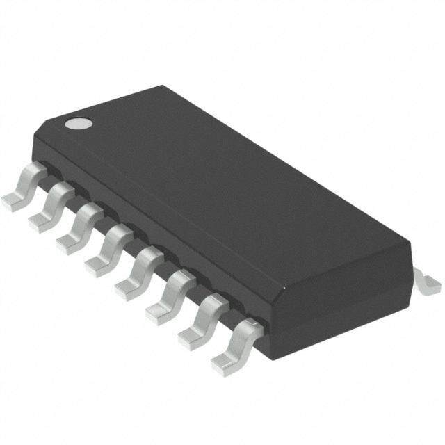
| 产品图片 |
|
| rohs | 符合RoHS无铅 / 符合限制有害物质指令(RoHS)规范要求 |
| 产品系列 | 电源管理 IC,低压差电压控制器,Texas Instruments LP2975IMM-5.0/NOPB- |
| 数据手册 | |
| 产品型号 | LP2975IMM-5.0/NOPB |
| 产品 | MOSFET LDO Driver/Controller |
| 产品种类 | 低压差电压控制器 |
| 供应商器件封装 | 8-VSSOP |
| 其它名称 | LP2975IMM-5.0/NOPBDKR |
| 包装 | Digi-Reel® |
| 商标 | Texas Instruments |
| 安装风格 | SMD/SMT |
| 封装 | Reel |
| 封装/外壳 | 8-TSSOP,8-MSOP(0.118",3.00mm 宽) |
| 封装/箱体 | VSSOP-8 |
| 工作温度 | -40°C ~ 125°C |
| 工厂包装数量 | 1000 |
| 最大工作温度 | + 125 C |
| 最大输入电压 | 24 V |
| 最小工作温度 | - 40 C |
| 最小输入电压 | 1.8 V |
| 标准包装 | 1 |
| 电压-输入 | 1.8 V ~ 24 V |
| 电压-输出 | 5V |
| 电流-电源 | 180µA |
| 电源电流 | 180 uA |
| 类型 | 正,固定式 |
| 系列 | LP2975 |
| 设计资源 | http://www.digikey.com/product-highlights/cn/zh/texas-instruments-webench-design-center/3176 |
| 输出数 | 1 |
| 输出类型 | Adjustable |



- 商务部:美国ITC正式对集成电路等产品启动337调查
- 曝三星4nm工艺存在良率问题 高通将骁龙8 Gen1或转产台积电
- 太阳诱电将投资9.5亿元在常州建新厂生产MLCC 预计2023年完工
- 英特尔发布欧洲新工厂建设计划 深化IDM 2.0 战略
- 台积电先进制程称霸业界 有大客户加持明年业绩稳了
- 达到5530亿美元!SIA预计今年全球半导体销售额将创下新高
- 英特尔拟将自动驾驶子公司Mobileye上市 估值或超500亿美元
- 三星加码芯片和SET,合并消费电子和移动部门,撤换高东真等 CEO
- 三星电子宣布重大人事变动 还合并消费电子和移动部门
- 海关总署:前11个月进口集成电路产品价值2.52万亿元 增长14.8%



PDF Datasheet 数据手册内容提取
LP2975 www.ti.com SNVS006F–SEPTEMBER1997–REVISEDAPRIL2013 MOSFET LDO Driver/Controller CheckforSamples:LP2975 FEATURES DESCRIPTION 1 • SimpletoUse,FewExternalComponents A high-current LDO regulator is simple to design with 2 theLP2975LDOController.UsinganexternalP-FET, • Ultra-smallVSSOP-8Package the LP2975 will deliver an ultra low dropout regulator • 1.5%(AGrade)PrecisionOutputVoltage withextremelylowquiescentcurrent. • Low-powerShutdownInput High open loop gain assures excellent regulation and • <1 µAinShutdown ripplerejectionperformance. • LowOperatingCurrent(180µATypical@V = IN The trimmed internal bandgap reference provides 5V) precise output voltage over the entire operating • WideSupplyVoltageRange(1.8Vto24V) temperaturerange. • Built-inCurrentLimitAmplifier Dropout voltage is “user selectable” by sizing the • OvertemperatureProtection external FET: the minimum input-output voltage required for operation is the maximum load current • 5.0V,and3.3VStandardOutputVoltages multipliedbytheR (ON)oftheFET. DS • CanbeProgrammedUsingExternalDivider Overcurrent protection of the external FET is easily • −40°Cto+125°CJunctionTemperatureRange implemented by placing a sense resistor in series withV .The57mVdetectionthresholdofthecurrent APPLICATIONS IN sense circuitry minimizes dropout voltage and power • High-current5Vto3.3VRegulator dissipationintheresistor. • PostRegulatorforSwitchingConverter The standard product versions available provide output voltages of 5.0V, or 3.3V with specified 25°C • Current-limitedSwitch accuracy of 1.5% (“A” grade) and 2.5% (standard grade). Block Diagram *R valuesare:208kfor12Vpart,72.8kfor5Vpart,and39.9kfor3.3Vpart. SET 1 Pleasebeawarethatanimportantnoticeconcerningavailability,standardwarranty,anduseincriticalapplicationsof TexasInstrumentssemiconductorproductsanddisclaimerstheretoappearsattheendofthisdatasheet. Alltrademarksarethepropertyoftheirrespectiveowners. 2 PRODUCTIONDATAinformationiscurrentasofpublicationdate. Copyright©1997–2013,TexasInstrumentsIncorporated Products conform to specifications per the terms of the Texas Instruments standard warranty. Production processing does not necessarilyincludetestingofallparameters.
LP2975 SNVS006F–SEPTEMBER1997–REVISEDAPRIL2013 www.ti.com Connection Diagram DevicePin6(N/C)hasnointernalconnection Figure1. 8-LeadVSSOPSurfaceMountPackage TopView SeePackageNumberDGK0008A 2 SubmitDocumentationFeedback Copyright©1997–2013,TexasInstrumentsIncorporated ProductFolderLinks:LP2975
LP2975 www.ti.com SNVS006F–SEPTEMBER1997–REVISEDAPRIL2013 Thesedeviceshavelimitedbuilt-inESDprotection.Theleadsshouldbeshortedtogetherorthedeviceplacedinconductivefoam duringstorageorhandlingtopreventelectrostaticdamagetotheMOSgates. ABSOLUTE MAXIMUM RATINGS(1) StorageTemperatureRange −65°Cto+150°C LeadTemp.(Soldering,5seconds) 260°C ESDRating 2kV PowerDissipation (2) InternallyLimited InputSupplyVoltage(Survival) −0.3Vto+26V CurrentLimitPins(Survival) −0.3Vto+V IN CompPin(Survival) −0.3Vto+2V GatePin(Survival) −0.3Vto+V IN ON/OFFPin(Survival) −0.3Vto+20V FeedbackPin(Survival) −0.3Vto+24V (1) AbsoluteMaximumRatingsindicatelimitsbeyondwhichdamagetothecomponentmayoccur.Electricalspecificationsdonotapply whenoperatingthedeviceoutsideofitsratedoperatingconditions. (2) TheLP2975hasinternalthermalshutdownwhichactivatesatadietemperatureofabout150°C.Itshouldbenotedthatthepower dissipatedwithintheLP2975islowenoughthatthisprotectioncircuitshouldneveractivateduetoself-heating,evenatelevated ambienttemperatures. OPERATING RATINGS JunctionTemperature,T −40°Cto+125°C J InputSupplyVoltage,V +1.8Vto+24V IN ELECTRICAL CHARACTERISTICS LimitsinstandardtypefaceareforT =25°C,andlimitsinboldfacetypeapplyoverthefulloperatingjunctiontemperature J range.Unlessotherwisespecified:V =1.5V,V =15V. ON/OFF IN LM2975AI-X.X LM2975I-X.X (1) (1) Symbol Parameter Conditions Typ Units Min Max Min Max RegulationVoltage 12.5<V <24V 11.820 12.180 11.700 12.300 IN 12.0 (12VVersions) (V -0.5V)>V >(V -5V) 11.640 12.360 11.520 12.480 IN GATE IN RegulationVoltage 5.5<V <24V 4.925 5.075 4.875 5.125 V IN 5.0 V REG (5VVersions) (V -0.5V)>V >(V -4.5V) 4.850 5.150 4.800 5.200 IN GATE IN RegulationVoltage 3.8<V <24V 3.250 3.350 3.217 3.383 IN 3.3 (3.3VVersions) (V -0.5V)>V >(V -3.3V) 3.201 3.399 3.168 3.432 IN GATE IN 1.215 1.265 1.203 1.277 V CompPinVoltage V <V <24V 1.240 V COMP REG IN 1.209 1.271 1.196 1.284 240 240 V =5V 180 I QuiescentCurrent IN 320 320 µA Q V =0V 0.01 1 1 ON/OFF CurrentLimit V =15V 45 69 45 69 V IN 57 mV CL SenseVoltage V =0.9XV 39 72 39 72 FB REG 1.10 1.10 Output=ON 0.94 1.20 1.20 V ON/OFFThreshold V ON/OFF 0.70 0.70 Output=OFF 0.87 0.40 0.40 ON/OFF 50 50 I V =1.5V 34 µA ON/OFF InputBiasCurrent ON/OFF 75 75 GateDriveCurrent V =7.5V 1.3 1.3 G 3.5 mA (Sourcing) V =1.1XV 0.3 0.3 FB REG I G GateDriveCurrent V =7.5V 350 350 G 1100 µA (Sinking) V =0.9XV 40 40 FB REG (1) Limitsare100%productiontestedat25°C.Limitsovertheoperatingtemperaturerangearespecifiedthroughcorrelationusing StatisticalQualityControl(SQC)methods.ThelimitsareusedtocalculateTI'sAverageOutgoingQualityLevel(AOQL). Copyright©1997–2013,TexasInstrumentsIncorporated SubmitDocumentationFeedback 3 ProductFolderLinks:LP2975
LP2975 SNVS006F–SEPTEMBER1997–REVISEDAPRIL2013 www.ti.com ELECTRICAL CHARACTERISTICS (continued) LimitsinstandardtypefaceareforT =25°C,andlimitsinboldfacetypeapplyoverthefulloperatingjunctiontemperature J range.Unlessotherwisespecified:V =1.5V,V =15V. ON/OFF IN LM2975AI-X.X LM2975I-X.X (1) (1) Symbol Parameter Conditions Typ Units Min Max Min Max V =24V V GateClampVoltage IN 17 15 19 15 19 V G(MIN) V =0.9XV FB REG Resistancefrom V =24V R(V -G) IN 500 kΩ IN GatetoV V =0 IN ON/OFF ΔVGATE/ OpenLoop VIN=15V 5000 V/V ΔVCOMP VoltageGain 0.5V≤VGATE≤13 4 SubmitDocumentationFeedback Copyright©1997–2013,TexasInstrumentsIncorporated ProductFolderLinks:LP2975
LP2975 www.ti.com SNVS006F–SEPTEMBER1997–REVISEDAPRIL2013 TYPICAL APPLICATION CIRCUITS *SeeApplicationHints:Feed-ForwardCapacitor. **Ifcurrentlimitingisnotrequired,shortoutthisresistor. Figure2. 5V-3.3V@5ALDORegulator *SeeApplicationHints:ADJUSTINGTHEOUTPUTVOLTAGE. ***Ifcurrentlimitingisnotrequired,shortoutthisresistor. Figure3. AdjustableVoltage5ALDORegulator Copyright©1997–2013,TexasInstrumentsIncorporated SubmitDocumentationFeedback 5 ProductFolderLinks:LP2975
LP2975 SNVS006F–SEPTEMBER1997–REVISEDAPRIL2013 www.ti.com TYPICAL PERFORMANCE CHARACTERISTICS Unlessotherwisespecified:T =25°C,C =1µF,ON/OFFpinistiedto1.5V. A IN MinimumOperatingVoltage V ReferredGateClampVoltage IN Figure4. Figure5. ON/OFFThreshold CurrentLimitSenseVoltage Figure6. Figure7. ON/OFFPinCurrent SupplyCurrent Figure8. Figure9. 6 SubmitDocumentationFeedback Copyright©1997–2013,TexasInstrumentsIncorporated ProductFolderLinks:LP2975
LP2975 www.ti.com SNVS006F–SEPTEMBER1997–REVISEDAPRIL2013 TYPICAL PERFORMANCE CHARACTERISTICS (continued) Unlessotherwisespecified:T =25°C,C =1µF,ON/OFFpinistiedto1.5V. A IN ON/OFFInputResistance GateCurrent Figure10. Figure11. Gate-GroundSaturation LineRegulation Figure12. Figure13. LoadRegulation LeakageCurrent Figure14. Figure15. Copyright©1997–2013,TexasInstrumentsIncorporated SubmitDocumentationFeedback 7 ProductFolderLinks:LP2975
LP2975 SNVS006F–SEPTEMBER1997–REVISEDAPRIL2013 www.ti.com TYPICAL PERFORMANCE CHARACTERISTICS (continued) Unlessotherwisespecified:T =25°C,C =1µF,ON/OFFpinistiedto1.5V. A IN ControllerGainandPhaseResponse Figure16. 8 SubmitDocumentationFeedback Copyright©1997–2013,TexasInstrumentsIncorporated ProductFolderLinks:LP2975
LP2975 www.ti.com SNVS006F–SEPTEMBER1997–REVISEDAPRIL2013 REFERENCE DESIGNS The LP2975 controller can be used with virtually any P-channel MOSFET to build a wide variety of linear voltage regulators. Since it would be impossible to document all the different voltage and current combinations that could be built, a numberofreferencedesignswillbepresentedalongwithperformancedataforeach. THE PERFORMANCE DATA SHOWN IS ACTUAL TEST DATA, BUT IS NOT ENSURED. The following reference designs have been confirmed with T = 25°C only, and no design consideration is given for operating A atanyotherambienttemperature. DESIGN #1: V = 5V @ 5A OUT (RefertoTYPICALAPPLICATIONCIRCUITS) Components C =82µFAluminumElectrolytic IN C =120µFAluminumElectrolytic OUT C =220pF F R =10mΩ SC P-FET=NDP6020P Heatsink: (assuming V ≤ 7V and T ≤ 60°C) if protection against a continuous short-circuit is required, a IN A heatsink with θ ≤ 1.5 °C/W must be used. However, if continuous short-circuit survivability is not needed, a S-A heatsinkwithθ ≤6°C/Wisadequate. S-A PerformanceData DropoutVoltage Dropout voltage is defined as the minumum input-to-output differential voltage required by the regulator to keep the output in regulation. It is measured by reducing V until the output voltage drops below the nominal value IN (thenominalvalueistheoutputvoltagemeasuredwithV =5.5V).I =5Aforthistest. IN L DROPOUTVOLTAGE=323mV LoadRegulation Load regulation is defined as the maximum change in output voltage as the load current is varied. It is measured by changing the load resistance and recording the minimum/maximum output voltage. The measured change in outputvoltageisdividedbythenominaloutputvoltageandexpressedasapercentage.V =5.6Vforthistest. IN 5mA≤I ≤5A:LOADREGULATION=0.012% L 0≤I ≤5A:LOADREGULATION=0.135% L LineRegulation Line regulation is defined as the maximum change in output voltage as the input voltage is varied. It is measured by changing the input voltage and recording the minimum/maximum output voltage. The measured change in outputvoltageisdividedbythenominaloutputvoltageandexpressedasapercentage.I =5Aforthistest. L 5.4V≤V ≤10V:LINEREGULATION=0.03% IN OutputNoiseVoltage Output noise voltage was measured by connecting a wideband AC voltmeter (HP 400E) directly across the outputcapacitor.V =6VandI =5Aforthistest. IN L NOISE=75µV(rms) Copyright©1997–2013,TexasInstrumentsIncorporated SubmitDocumentationFeedback 9 ProductFolderLinks:LP2975
LP2975 SNVS006F–SEPTEMBER1997–REVISEDAPRIL2013 www.ti.com TransientResponse Transient response is defined as the change in output voltage which occurs after the load current is suddenly changed.V =5.6Vforthistest. IN The load resistor is connected to the regulator output using a switch so that the load current increases from 0 to 5A abruptly. The change in output voltage is shown in the scope photo below (the vertical scale is 200 mV/division and the horizontal scale is 10 µs/division). The regulator nominal output (5V) is located on the center lineofthephoto. The output shows a maximum change of about −600 mV compared to nominal. This is due to the relatively small output capacitor chosen for this design. Increasing C greatly improves transient response (see Design #2 and OUT Design#3). Figure17. TransientResponsefor0–5ALoadStep DESIGN #2: V = 3V @ 0.5A OUT (RefertoTYPICALAPPLICATIONCIRCUITS,AdjustableVoltageRegulator) Components C =68µFTantalum IN C =2X68µFTantalum OUT C =470pF C R1=237kΩ,1% R2=NOTUSED R =0.1Ω SC TiefeedbackpintoV OUT P-FET=NDT452P Heatsink:TabofN-FETissoldereddownto0.6in2copperareaonPCboard. Output Voltage Adjustment: For this application, a 3.3V part is “trimmed” down to 3V by using a single external 237kΩ resistoratR1,whichparallelstheinternal39.9kΩ resistor(reducingtheeffectiveresistanceto34.2kΩ). Because the tempco of the external resistor will not match the tempco of the internal resistor (which is typically 3000 ppm), this method of adjusting V by using a single resistor is only recommended in cases where the OUT outputvoltageisadjusted≤ 10%awayfromthenominalvalue. 10 SubmitDocumentationFeedback Copyright©1997–2013,TexasInstrumentsIncorporated ProductFolderLinks:LP2975
LP2975 www.ti.com SNVS006F–SEPTEMBER1997–REVISEDAPRIL2013 PerformanceData DropoutVoltage Dropout voltage is defined as the minimum input-to-output differential voltage required by the regulator to keep the output in regulation. It is measured by reducing V until the output voltage drops below the nominal value IN (thenominalvalueistheoutputvoltagemeasuredwithV =5V).I =0.5Aforthistest. IN L DROPOUTVOLTAGE=141mV LoadRegulation Load regulation is defined as the maximum change in output voltage as the load current is varied. It is measured by changing the load resistance and recording the minimum/maximum output voltage. The measured change in outputvoltageisdividedbythenominaloutputvoltageandexpressedasapercentage.V =3.5Vforthistest. IN 0≤I ≤0.5A:LOADREGULATION=0.034% L LineRegulation Line regulation is defined as the maximum change in output voltage as the input voltage is varied. It is measured by changing the input voltage and recording the minimum/maximum output voltage. The measured change in outputvoltageisdividedbythenominaloutputvoltageandexpressedasapercentage.I =0.5Aforthistest. L 3.5V≤V ≤6V:LINEREGULATION=0.017% IN OutputNoiseVoltage Output noise voltage was measured by connecting a wideband AC voltmeter (HP 400E) directly across the outputcapacitor.V =5VandI =0.5Aforthistest. IN L NOISE=85µV(rms) TransientResponse Transient response is defined as the change in output voltage which occurs after the load current is suddenly changed.V =3.5Vforthistest. IN The load resistor is connected to the regulator output using a switch so that the load current increases from 0 to 0.5A abruptly. The change in output voltage is shown in the scope photo (the vertical scale is 20 mV/division and the horizontal scale is 50 µs/division). The regulator nominal output (3V) is located on the center line of the photo.Amaximumchangeofabout−50mVisshown. Figure18. TransientResponsefor0–0.5ALoadStep MinimizingC OUT It is often desirable to decrease the value of C to save cost and reduce size. The design guidelines suggest OUT selecting C to set the first pole ≤ 200 Hz (see later section, Output Capacitor), but this is not an absolute OUT requirementinallcases. Copyright©1997–2013,TexasInstrumentsIncorporated SubmitDocumentationFeedback 11 ProductFolderLinks:LP2975
LP2975 SNVS006F–SEPTEMBER1997–REVISEDAPRIL2013 www.ti.com The effect of reducing C is to decrease phase margin. As phase margin is decreased, the output ringing will OUT increase when a load step is applied to the output. Eventually, if C is made small enough, the regulator will OUT oscillate. To demonstrate these effects, the value of C in reference design #2 is halved by removing one of the two 68 OUT µF output capacitors and the transient response test is repeated (see photo below). The total overshoot increasesfrom−50mVtoabout −75mV,andthesecond“ring” onthetransientisnoticeablylarger. Figure19. TransientResponsewithOutputCapacitorHalved The design is next tested with only a 4.7 µF output capacitor (see scope photo below). Observe that the vertical scale has been increased to 100 mV/division to accommodate the −250 mV undershoot. More important is the severeringingasthetransientdecays.Mostdesignerswouldrecognizethisimmediatelyasthewarningsignofa marginallystabledesign. Figure20. TransientResponsewithOnly4.7µFOutputCap The reason this design is marginally stable is that the 4.7 µF output capacitor (along with the 6Ω output load) sets the pole f at 5 kHz. Analysis shows that the unity-gain frequency of the loop is increased to about 100 kHz, p allowing the FET's gate capacitance pole f to cause significant phase shift before the loop gain goes below pg unity. Also, because of the low output voltage, the feedforward capacitor provides less than 10° of positive phase shift.Forgoodstability,theoutputcapcitorneedstobelargerthan4.7µF. Fordetailedinformationonstabilityandphasemargin,seetheApplicationHintssection. 12 SubmitDocumentationFeedback Copyright©1997–2013,TexasInstrumentsIncorporated ProductFolderLinks:LP2975
LP2975 www.ti.com SNVS006F–SEPTEMBER1997–REVISEDAPRIL2013 DESIGN #3: V = 1.5V @ 6A. OUT (RefertoTYPICALAPPLICATIONCIRCUITS,AdjustableVoltageRegulator) Components C =1000µFAluminumElectrolytic IN C =4X330µFOSCONAluminumElectrolytic OUT C =NOTUSED C R1=261Ω,1% R2=1.21kΩ,1% R =6mΩ SC P-FET=NDP6020P Heatsink: (Assuming V ≤ 3.3V and T ≤ 60°C) if protection against a continuous short-circuit is required, a IN A heatsink with θ < 2.5 °C/W must be used. However, if continuous short-circuit survivability is not needed, a S-A heatsinkwithθ <7°C/Wisadequate. S-A PerformanceData DropoutVoltage Dropout voltage is defined as the minimum input-to-output differential voltage required by the regulator to keep the output in regulation. It is measured by reducing V until the output voltage drops below the nominal value IN (thenominalvalueistheoutputvoltagemeasuredwithV =3.3V).I =6Aforthistest. IN L DROPOUTVOLTAGE=0.68V LoadRegulation Load regulation is defined as the maximum change in output voltage as the load current is varied. It is measured by changing the load resistance and recording the minimum/maximum output voltage. The measured change in outputvoltageisdividedbythenominaloutputvoltageandexpressedasapercentage.V =3.3Vforthistest. IN 0≤I ≤6A:LOADREGULATION=0.092% L LineRegulation Line regulation is defined as the maximum change in output voltage as the input voltage is varied. It is measured by changing the input voltage and recording the minimum/maximum output voltage. The measured change in outputvoltageisdividedbythenominaloutputvoltageandexpressedasapercentage.I =6Aforthistest. L 3.3V≤V ≤5V:LINEREGULATION=0.033% IN OutputNoiseVoltage Output noise voltage was measured by connecting a wideband AC voltmeter (HP 400E) directly across the outputcapacitor.V =3.3VandI =6Aforthistest. IN L NOISE=60µV(rms) TransientResponse Transient response is defined as the change in output voltage which occurs after the load current is suddenly changed.V =3.3Vforthistest. IN The load resistor is connected to the regulator output using a switch so that the load current increases from 0 to 6A abruptly. The change in output voltage is shown in the scope photo (the vertical scale is 50 mV/division and the horizontal scale is 20 µs/division. The regulator nominal output (1.5V) is located on the center line of the photo.Amaximumchangeofabout−80mVisshown. Copyright©1997–2013,TexasInstrumentsIncorporated SubmitDocumentationFeedback 13 ProductFolderLinks:LP2975
LP2975 SNVS006F–SEPTEMBER1997–REVISEDAPRIL2013 www.ti.com Figure21. TransientResponsefor0–6ALoadStep Application Hints SELECTINGTHEFET ThebestchoiceofFETforaspecificapplicationwilldependonanumberoffactors: VOLTAGE RATING: The FET must have a Drain-to-Source breakdown voltage (sometimes called BV ) which DSS isgreaterthantheinputvoltage. DRAIN CURRENT: On-state Drain current must be specified to be greater than the worst-case (short circuit) loadcurrentfortheapplication. TURN-ON THRESHOLD: The Gate-to-Source voltage where the FET turns on (called the Gate Threshold Voltage) is very important. Many FET's are intended for use with G-to-S voltages in the 5V to 10V range. These shouldonlybeusedinapplicationswheretheinputvoltageishighenoughtoprovide>5VofdrivetotheGate. Newer FET's are becoming available with lower turn-on thresholds (Logic-Level FET's) which turn on fully with a gate voltage of only 3V to 4V. Low threshold FET's should be used in applications where the input voltage is ≤ 5V. ONRESISTANCE:FETonresistance(oftencalledR ON)isacriticalparametersinceitdirectlydeterminesthe DS minimuminput-to-outputvoltagerequiredforoperationatagivenloadcurrent(alsocalleddropoutvoltage). R ON is highly dependent on the amount of Gate-to-Source voltage applied. For example, the R ON of a FET DS DS with V = 5V will typically decrease by about 25% as the V is increased to 10V. R ON is also temperature G-S G-S DS dependent,increasingathighertemperatures. ThedropoutvoltageofanyLDOdesignisdirectlyrelatedtoR ON,asgivenby: DS V =I ×(R ON+R ) DROPOUT LOAD DS SC where • R istheshort-circuitcurrentlimitsetresistor(seeTYPICALAPPLICATIONCIRCUITS) SC GATE CAPACITANCE: Selecting a FET with the lowest possible Gate capacitance improves LDO performance intwoways: 1. The Gate pin of the LP2975 (which drives the Gate of the FET) has a limited amount of current to source or sink. This means faster changes in Gate voltage (which corresponds to faster transient response) will occur withasmalleramountofGatecapacitance. 2. The Gate capacitance forms a pole in the loop gain which can reduce phase margin. When possible, this pole should be kept at a higher frequency than the cross-over frequency of the regulator loop (see later section,CrossoverFrequencyandPhaseMargin). AhighvalueofGatecapacitancemayrequirethatafeedforwardcapacitorbeusedtocancelsomeoftheexcess phaseshift(seelatersection,Feed-ForwardCapacitor)topreventloopinstability. 14 SubmitDocumentationFeedback Copyright©1997–2013,TexasInstrumentsIncorporated ProductFolderLinks:LP2975
LP2975 www.ti.com SNVS006F–SEPTEMBER1997–REVISEDAPRIL2013 POWERDISSIPATION:ThemaximumpowerdissipatedintheFETinanyapplicationcanbecalculatedfrom: P =(V −V )×I MAX IN OUT MAX where • I isthemaximumoutputcurrent MAX It should be noted that if the regulator is to be designed to withstand short-circuit, a current sense resistor must beusedtolimitI toasafevalue(refertosectionSHORT-CIRCUITCURRENTLIMITING). MAX The power dissipated in the FET determines the best choice for package type. A TO-220 package device is best suitedforapplicationswherepowerdissipationislessthan15W.Powerlevelsabove15Wwouldalmostcertainly requireaTO-3typedevice. In low power applications, surface-mount package devices are size-efficient and cost-effective, but care must be takentonotexceedtheirpowerdissipationlimits. POWERDISSIPATIONANDHEATSINKING SincetheLP2975controllerissuitableforusewithalmostanyexternalP-FET,itfollowsthatdesignscanbebuilt which have very high power dissipation in the pass FET. Since the controller can not protect the FET from overtemperaturedamage,thermaldesignmustbecarefullydonetoassureareliabledesign. THERMALDESIGNMETHOD:ThetemperatureoftheFETandthepowerdissipatedisdefinedbytheequation: T =(θ ×P )+T J J-A D A where • T isthejunctiontemperatureoftheFET. J • T istheambienttemperature. A • P isthepowerdissipatedbytheFET. D • θ isthejunction-to-ambientthermalresistance. J-A Toensureareliabledesign,thefollowingguidelinesarerecommended: 1. Designforamaximum(worst-case)FETjunctiontemperaturewhichdoesnotexceed150°C. 2. Heatsinkingshouldbedesignedforworst-case(maximum)valuesofT andP . A D 3. In designs which must survive a short circuit on the output, the maximum power dissipation must be calculatedassumingthattheoutputisshortedtoground: P (MAX)=V ×I D IN SC where • I istheshort-circuitoutputcurrent. SC 4. If the design is not intended to be short-circuit proof, the maximum power dissipation for intended operation willbe: P (MAX)=(V −V )×I D IN OUT MAX where • I isthemaximumoutputcurrent. MAX LOW POWER (<2W) APPLICATIONS: In most cases, some type of small surface-mount device will be used for the FET in low power designs. Because of the increased cell density (and tiny packages) used by modern FET's, the current carrying capability may easily exceed the power dissipation limits of the package. It is possible to paralleltwoormoreFET's,whichdividesthepowerdissipationamongallofthepackages. It should be noted that the “heatsink” for a surface mount package is the copper of the PC board and the packageitself(directradiation). Surface-mount devices have the value of θ specified for a typical PC board mounting on their data sheet. In J-A most cases it is best to start with the known data for the application (P , T , T ) and calculate the required value D A J ofθ needed.ThisvaluewilldefinethetypeofFETand,possibly,theheatsinkrequiredforcooling. J-A θ =(T −T )/P (MAX) J-A J A D Copyright©1997–2013,TexasInstrumentsIncorporated SubmitDocumentationFeedback 15 ProductFolderLinks:LP2975
LP2975 SNVS006F–SEPTEMBER1997–REVISEDAPRIL2013 www.ti.com DESIGN EXAMPLE: A design is to be done with V = 5V and V = 3.3V with a maximum load current of 300 IN OUT mA.Basedontheseconditions,powerdissipationintheFETduringnormaloperationwouldbe: P =(V −V )×I D IN OUT LOAD Solving, we find that P = 0.51W. Assuming that the maximum allowable value of T is 150°C and the maximum D J T is70°C,thevalueofθ isfoundtobe157°C/W. A J-A However,ifthisdesignmustsurviveacontinuousshortontheoutput,thepowerdissipatedintheFETishigher: P (SC)=V ×I =5×0.33=1.65W D IN SC (ThisassumesthecurrentsenseresistorisselectedforanI valuethatis10%higherthantherequired0.3A). SC Thevalueofθ requiredtosurvivecontinuousshortcircuitiscalculatedtobe49°C/W. J-A Having solved for the value(s) of θ , a FET can be selected. It should be noted that a FET must be used with a J-A θ valuelessthanorequaltothecalculatedvalue. J-A HIGH POWER (≥2W) APPLICATIONS: As power dissipation increases above 2W, a FET in a larger package must be used to obtain lower values of θ . The same formulae derived in the previous section are used to J-A calculateP andθ . D J-A Having found θ , it becomes necessary to calculate the value of θ (the heatsink-to-ambient thermal J-A S-A resistance)sothataheatsinkcanbeselected: θ =θ −(θ +θ ) S-A J-A J-C C-S where • θ isthejunction-to-casethermalresistance.Thisparameteristhemeasureofthermalresistancebetween J-C thesemiconductordieinsidetheFETandthesurfaceofthecaseoftheFETwhereitmountstotheheatsink (thevalueofθ canbefoundonthedatasheetfortheFET).AtypicalFETinaTO-220packagewillhavea J-C θ valueofapproximately2–4°C/W,whileadeviceinaTO-3packagewillbeabout0.5–2°C/W. J-C • θ isthecase-to-heatsinkthermalresistance,whichmeasureshowmuchthermalresistanceexistsbetween C-S thesurfaceoftheFETandtheheatsink.θ isdependentonthepackagetypeandmountingmethod.ATO- C-S 220packagewithmicainsulatorandthermalgreasesecuredtoaheatsinkwillhaveaθ valueintherange C-S of1–1.5°C/W.ATO-3packagemountedinthesamemannerwillhaveaθ valueof0.3–0.5°C/W.Thebest C-S sourceofinformationforthisisheatsinkcatalogs(Wakefield,AAVID,Thermalloy)sincetheyalsosell mountinghardware. • θ istheheatsink-to-ambientthermalresistance,whichdefineshowwellaheatsinktransfersheatintothe S-A air.Oncethisisdetermined,aheatsinkmustbeselectedwhichhasavaluewhichislessthanorequaltothe computedvalue. The value of θ is usually listed in the manufacturer's data sheet for a heatsink, but the information is S-A sometimesgiveninagraphoftemperaturerisevs.dissipatedpower. DESIGN EXAMPLE: A design is to be done which takes 3.3V in and provides 2.5V out at a load current of 7A. Thepowerdissipationwillbecalculatedforbothnormaloperationandshortcircuitconditions. Fornormaloperation: P =(V −V )×I =5.6W D IN OUT LOAD Iftheoutputisshortedtoground: P (SC)=V ×I =3.3×7.7=25.4W D IN SC (AssumingthatasenseresistorisselectedtosetthevalueofI 10%abovethenominal7A). SC θ willbecalculatedassumingamaximumT of70°CandamaximumT of150°C: J-A A J θ =(T −T )/P (MAX) J-A J A D Fornormaloperation: θ =(150−70)/5.6=14.3°C/W J-A Fordesignswhichmustoperatewiththeoutputshortedtoground: θ =(150−70)/25.4=3.2°C/W J-A 16 SubmitDocumentationFeedback Copyright©1997–2013,TexasInstrumentsIncorporated ProductFolderLinks:LP2975
LP2975 www.ti.com SNVS006F–SEPTEMBER1997–REVISEDAPRIL2013 The value of 14.3°C/W can be easily met using a TO-220 device. Calculating the value of θ required S-A (assumingavalueofθ =3°C/Wandθ =1°C/W): J-C C-S θ =θ −(θ +θ ) S-A J-A J-C C-S θ =14.3−(3+1)=10.3°C/W S-A Any heatsink may be used with a thermal resistance ≤ 10.3°C/W @ 5.6W power dissipation (refer to manufacturer's data sheet curves). Examples of suitable heatsinks are Thermalloy #6100B and IERC #LATO127B5CB. However, if the design must survive a sustained short on the output, the calculated θ value of 3.2°C/W J-A eliminatesthepossibilityofusingaTO-220packagedevice. Assuming a TO-3 device is selected with a θ value of 1.5°C/W and θ = 0.4°C/W, we can calculate the J-C C-S requiredvalueofθ : S-A θ =θ −(θ +θ ) S-A J-A J-C C-S θ =3.2−(1.5+0.4)=1.3°C/W S-A A θ value ≤1.3°C/W would require a relatively large heatsink, or possibly some kind of forced airflow for S-A cooling. SHORT-CIRCUITCURRENTLIMITING Short-circuit current limiting is easily implemented using a single external resistor (R ). The value of R can be SC SC calculatedfrom: R =V /I SC CL SC where • I isthedesiredshortcircuitcurrent. SC • V isthecurrentlimitsensevoltage. CL The value of V is 57 mV (typical), with specified limits listed in the ELECTRICAL CHARACTERISTICS section. CL When doing a worst-case calculation for power dissipation in the FET, it is important to consider both the toleranceofV andthetolerance(andtemperaturedrift)ofR . CL SC For maximum accuracy, the INPUT and CURRENT LIMIT pins must be Kelvin connected to R , to avoid errors SC causedbyvoltagedropsalongthetracescarryingthecurrentfromtheinputsupplytotheSourcepinoftheFET. EXTERNALCAPACITORS The best capacitors for use in a specific design will depend on voltage and load current (examples of tested circuitsforseveraldifferentoutputvoltagesandcurrentsareprovidedinaprevioussection.) Informationinthenextsectionsisprovidedtoaidthedesignerintheselectionoftheexternalcapacitors. InputCapacitor Although not always required, an input capacitor is recommended. Good bypassing on the input assures that the regulator is working from a source with a low impedance, which improves stability. A good input capacitor can also improve transient response by providing a reservoir of stored energy that the regulator can utilize in cases wheretheloadcurrentdemandsuddenlyincreases.ThevalueusedforC maybeincreasedwithoutlimit.Refer IN totheREFERENCEDESIGNSsectionforexamplesofinputcapacitors. OutputCapacitor The output capacitor is required for loop stability (compensation) as well as transient response. During sudden changes in load current demand, the output capacitor must source or sink current during the time it takes the control loop of the LP2975 to adjust the gate drive to the pass FET. As a general rule, a larger output capacitor will improve both transient response and phase margin (stability). The value of C may be increased without OUT limit. OUTPUT CAPACITOR AND COMPENSATION: Loop compensation for the LP2975 is derived from C and, in OUT somecases,thefeed-forwardcapacitorC (seenextsection). F Copyright©1997–2013,TexasInstrumentsIncorporated SubmitDocumentationFeedback 17 ProductFolderLinks:LP2975
LP2975 SNVS006F–SEPTEMBER1997–REVISEDAPRIL2013 www.ti.com C forms a pole (referred to as f ) in conjuction with the load resistance which causes the loop gain to roll off OUT p (decrease)atanadditional−20dB/decade.Thefrequencyofthepoleis: f =0.16/[(R +ESR)×C ] p L OUT where • R istheloadresistance. L • C isthevalueoftheoutputcapacitor. OUT • ESRistheequivalentseriesresistanceofC . OUT As a general guideline, the frequency of f should be ≤ 200 Hz. It should be noted that higher load currents p correspondtolowervaluesofR ,whichrequiresthatC beincreasedtokeepf atagivenfrequency. L OUT p DESIGN EXAMPLE: Select the minimum required output capacitance for a design whose output specifications are5V@1A: f =0.16/[(R +ESR)×C ] p L OUT Re-written: C =0.16/[f ×(R +ESR)] OUT p L Valuesusedforthecalculation: f =200Hz,R =5Ω,ESR=0.1Ω (assumed). p L SolvingforC ,weget157μF(neareststandardsizewouldbe180 μF). OUT The ESR of the output capacitor is very important for stability, as it creates a zero (f ) which cancels much of the z phaseshiftresultingfromoneofthepolespresentintheloop.Thefrequencyofthezeroiscalculatedfrom: f =0.16/(ESR×C ) z OUT For best results in most designs, the frequency of f should fall between 5 kHz and 50 kHz. It must be noted that z the values of C and ESR usually vary with temperature (severely in the case of aluminum electrolytics), and OUT thismustbetakenintoconsideration. For the design example (V = 5V @ 1A), select a capacitor which meets the f requirements. Solving the OUT z equationforESRyields: ESR=0.16/(f ×C ) z OUT Assumingf =5kHzand50kHz,thelimitingvaluesofESRforthe180μFcapacitorarefoundtobe: z 18mΩ≤ESR≤0.18Ω A good-quality, low-ESR capacitor type such as the Panasonic HFQ is a good choice. However, the 10V/180 µF capacitor(#ECA-1AFQ181)hasanESRof0.3Ω whichisnotinthedesiredrange. Toassureastabledesign,someoftheoptionsare: 1. UseadifferenttypecapacitorwhichhasalowerESRsuchasanorganic-electrolyteOSCON. 2. Use a higher voltage capacitor. Since ESR is inversely proportional to the physical size of the capacitor, a higher voltage capacitor with the same C value will typically have a lower ESR (because of the larger case size). In this example, a Panasonic ECA-1EFQ181 (which is a 180 µF/25V part) has an ESR of 0.17Ω and wouldmeetthedesiredESRrange. 3. Useafeed-forwardcapacitor(seenextsection). Feed-ForwardCapacitor Although not required in every application, the use of a feed-forward capacitor (C ) can yield improvements in F bothphasemarginandtransientresponseinmostdesigns. The added phase margin provided by C can prevent oscillations in cases where the required value of C and F OUT ESRcannotbeeasilyobtained(seeprevioussection). C can also reduce the phase shift due to the pole resulting from the Gate capacitance, stabilizing applications F where this pole occurs at a low frequency (before cross-over) which would cause oscillations if left uncompensated(seelatersection,GateCapacitancePoleFrequency(f ). pg Even in a stable design, adding C will typically provide more optimal loop response (faster settling time). For F thesereasons,theuseofafeed-forwardcapacitorisalwaysrecommended. 18 SubmitDocumentationFeedback Copyright©1997–2013,TexasInstrumentsIncorporated ProductFolderLinks:LP2975
LP2975 www.ti.com SNVS006F–SEPTEMBER1997–REVISEDAPRIL2013 C is connected across the top resistor in the divider used to set the output voltage (see TYPICAL F APPLICATIONCIRCUITS).Thisformsazerointheloopresponse(definedasf ),whosefrequencyis: zf f =6.6×10⁻⁶/[C ×(V /1.24−1)] zf F OUT WhensolvedforC ,thef equationis: F zf C =6.6×10⁻⁶/[f ×(V /1.24−1)] F zf OUT Formostapplications,f shouldbesetbetween5kHzand50kHz. zf ADJUSTINGTHEOUTPUTVOLTAGE If an output voltage is required which is not available as a standard voltage, the LP2975 can be configured as an adjustable regulator (see TYPICAL APPLICATION CIRCUITS). The external resistors R1 and R2 (along with the internal24kΩresistor)settheoutputvoltage. The use of any external resistors to alter the LP2975 pre-set output voltage is outside the specified operating conditions.Outputvoltageaccuracywithexternalresistorswillbeinferiorwhencomparedtothetolerancesofthe LP2975 pre-set voltages options, and some external trim mechanism may be needed to achieve an acceptable initial accuracy of the custom output voltage. Users of this methodology are strongly encouraged to confirm that theircustomcircuitmeetsalloftheirperformancerequirements. It is important to note that the external R2 is connected in parallel with the internal 24 kΩ resistor (typical). If we define R as the total resistance between the COMP pin and ground, then its value will be the parallel EQ combinationofR2and24kΩ: R =(R2×24k)/(R2+24k) EQ Itfollowsthattheoutputvoltagewillbe: V =1.24[(R1/R )+1] OUT EQ SomeimportantconsiderationsforanadjustableLP2975design: The tolerance of the internal 24 kΩ resistor is about ±20%. Also, its temperature coefficient is almost certainly differentthantheTCofanyexternalresistorthatisusedforR2. For these reasons, it is recommended that R2 be set at a value that is not greater than 1.2k. In this way, the value of R2 will dominate R , and the tolerance and TC of the internal 24k resistor will have a negligible effect EQ onoutputvoltageaccuracy. While this guideline for the value of R2 will generally provide adequate performance when operating with T = A 25°C, it is important to note that loading the COMP pin with 1.2kΩ, or less, to ground will impair device operation at elevated temperatures. For operation at temperatures above approximately 50°C it is recommended that the valueofR2shouldnotbelessthanapproximately5kΩ. TodeterminethevalueforR1: R1=R [(V /1.24)−1] EQ OUT ExternalCapacitors(AdjustableApplication) All information in the previous section, EXTERNAL CAPACITORS, applies to the adjustable application with the exceptionofhowtoselectthevalueofthefeed-forwardcapacitor. The feed-forward capacitor C in the adjustable application (see TYPICAL APPLICATION CIRCUITS) performs C exactly the same function as described in the previous section, Feed-Forward Capacitor. However, because R1 isuser-selected,adifferentformulamustbeusedtodeterminethevalueofC : C C =1/(2π×R1×f ) C zf Asstatedpreviously,theoptimalfrequencyatwhichtoplacethezerof isusuallybetween5kHzand50kHz. zf OPTIMIZINGDESIGNSTABILITY Because the LP2975 can be used with a variety of different applications, there is no single set of components that are best suited to every design. This section provides information which will enable the designer to select componentsthatoptimizestability(phasemargin)foraspecificapplication. Copyright©1997–2013,TexasInstrumentsIncorporated SubmitDocumentationFeedback 19 ProductFolderLinks:LP2975
LP2975 SNVS006F–SEPTEMBER1997–REVISEDAPRIL2013 www.ti.com GateCapacitance An important consideration of a design is to identify the frequency of the pole which results from the capacitance of the Gate of the FET (this pole will be referred to as f ). As f gets closer to the loop crossover frequency, the pg pg phasemarginisreduced.InformationwillnowbeprovidedtoallowthetotalGatecapacitancetobecalculatedso thatf canbeapproximated. pg The first step in calculating fp is to determine how much effective Gate capacitance (C ) is present. The EFF formulaforcalculatingC is: EFF C =C +C [1+G (R //ESR)] EFF GS GD m L where • C istheGate-to-Sourcecapacitance,whichisfoundfromthevalues(refertoFETdatasheetforvaluesof GS C andC ): ISS RSS C =C −C GS ISS RSS where • G istheGate-to-Draincapacitance,whichisequalto: GD C =C GD RSS where • G isthetransconductanceoftheFET. m The FET data sheet specifies forward transconductance (G ) at some value of drain current (defined as I ). To fs D findGmatthedesiredvalueofloadcurrent(definedasI ),usetheformula: L G =G ×(I /I )1/2 m fs L D where • R istheloadresistance. L ESRistheequivalentseriesresistanceoftheoutputcapacitor. • ThetermR //ESRisdefinedas: L (R ×ESR)/(R +ESR) L L It can be seen from these equations that C varies with R . To get the worst-case (maximum) value for C , EFF L EFF use the maximum value of load current, which also means the minimum value of load resistance R . It should be L notedthatinmostcases,theESRisthedominanttermwhichdeterminesthevalueofR //ESR. L Figure22. GatePinOutputImpedance GateCapacitancePoleFrequency(f ) pg ThepolefrequencyresultingfromtheGatecapacitanceC isdefinedasf andcanbeapproximatedfrom: EFF pg f ≃0.16/(R ×C ) pg O EFF where • R istheoutputimpedanceoftheLP2975GatepinwhichdrivestheGateoftheFET. O 20 SubmitDocumentationFeedback Copyright©1997–2013,TexasInstrumentsIncorporated ProductFolderLinks:LP2975
LP2975 www.ti.com SNVS006F–SEPTEMBER1997–REVISEDAPRIL2013 It is important to note that R is a function of input supply voltage (see Figure 22. As shown, the minimum value O ofR isabout550Ω @V =24V,increasingtoabout1.55kΩ@V =3V. O IN IN Using the equation for f , a family of curves are provided showing how f varies with C for several values of pg pg EFF R (seeFigure23). O Figure23. f vs.C pg EFF Ascanbeseeninthegraph,valuesofC inthe500pF–2500pFrangeproducevaluesforf between40kHz EFF pg and 700 kHz. To determine what effect f will have on stability, the bandwidth of the regulator loop must be pg calculated(seenextsection,CrossoverFrequencyandPhaseMargin). CrossoverFrequencyandPhaseMargin Thetermf willbeusedtodefinethecrossoverfrequencyoftheregulatorloop(whichisthefrequencywherethe c gain curve crosses the 0 dB axis). The importance of this frequency is that it is the point where the loop gain goesbelowunity,whichmarkstheusablebandwidthoftheregulatorloop. Itisthephasemargin(orlackofit)atf thatdetermineswhethertheregulatorisstable.Phasemarginisdefined c as the total phase shift subtracted from 180°. In general, a stable loop requires at least 20°-30° of phase margin atf . c f canbeapproximatedbythefollowingequation(alltermshavebeenpreviouslydefined): c ThisequationassumesthatnoC isusedandf /f >1. F pg c If the frequency of the Gate capacitance pole f has been calculated (previous section), the amount of added pg phase shift may now be determined. As shown in the graph below (see Figure 24, the amount of added phase shiftincreasesasf approachesf . pg c The amount of phase shift due to f that can occur before oscillation takes place depends on how much added pg phaseshiftispresentasaresultoftheC pole(seeprevioussection,OutputCapacitor). OUT Copyright©1997–2013,TexasInstrumentsIncorporated SubmitDocumentationFeedback 21 ProductFolderLinks:LP2975
LP2975 SNVS006F–SEPTEMBER1997–REVISEDAPRIL2013 www.ti.com Figure24. PhaseShiftDuetof pg Because of this, there is no exact number for f /f that can be given as a fixed limit for stable operation. pg c However,asageneralguideline,itisrecommendedthatf ≥3f . pg c If this is not found to be true after inital calculations, the ratio of f /f can be increased by either reducing C pg c EFF (selectingadifferentFET)orusingalargervalueofC . OUT Along with these two methods, another technique for improving loop stability is the use of a feed-forward capacitor (see next section, Feed-Forward Compensation). This can improve phase margin by cancelling some oftheexcessphaseshift. Feed-ForwardCompensation Phase shift in the loop gain of the regulator results from f (the pole from the output capacitor and load p resistance), f (the pole from the FET gate capacitance), as well as the IC's internal controller pole (see typical pg curve).Ifthetotalphaseshiftbecomesexcessive,instabilitycanresult. Thetotalphaseshiftcanbereducedusingfeed-forwardcompensation,whichplacesazerointhelooptoreduce theeffectsofthepoles. The feed-forward capacitor C can accomplish this, provided it is selected to set the zero at the correct F frequency. It is important to point out that the feed-forward capacitor produces both a zero and a pole. The frequency where the zero occurs will be defined as f , and the frequency of the pole will be defined as f . The zf pf equationstocalculatethefrequenciesare: f =6.6×10⁻⁶/[C ×(V /1.24−1)] zf F OUT f =6.6×10⁻⁶/[C ×(1−1.24/V )] pf F OUT In general, the feed-forward capacitor gives the greatest improvement in phase margin (provides the maximum reduction in phase shift) when the zero occurs at a frequency where the loop gain is >1 (before the crossover frequency). The pole must occur at a higher frequency (the higher the better) where most of the phase shift added by the new pole occurs beyond the crossover frequency. For this reason, the pole-zero pair created by C F becomemoreeffectiveatimprovingloopstabilityastheygetfartherapartinfrequency. In reviewing the equations for f and f , it can be seen that they get closer together in frequency as V zf pf OUT decreases. For this reason, the use of C gives greatest benefit at higher output voltages, declining as V F OUT approaches1.24V(whereC hasnoeffectatall). F In selecting a value of feed-forward capacitor, the crossover frequency f must first be calculated. In general, the c frequencyofthezero(f )setbythiscapacitorshouldbeintherange: zf 0.2f ≤f ≤1.0f c zf c Theequationtodeterminethevalueofthefeed-forwardcapacitorinfixed-voltageapplicationsis: C =6.6×10⁻⁶/[f ×(V /1.24−1)] F zf OUT Inadjustableapplications(usinganexternalresistivedivider)thecapacitorisfoundusing: C =1/(2π×R1×f ) C zf 22 SubmitDocumentationFeedback Copyright©1997–2013,TexasInstrumentsIncorporated ProductFolderLinks:LP2975
LP2975 www.ti.com SNVS006F–SEPTEMBER1997–REVISEDAPRIL2013 SummaryofStabilityInformation This section will present an explanation of theory and terminology used to analyze loop stability, along with specificinformationrelatedtostabilizingLP2975applications. BodePlotsandPhaseShift Loop gain information is most often presented in the form of a Bode Plot, which plots Gain (in dB) versus Frequency(inHertz). A Bode Plot also conveys phase shift information, which can be derived from the locations of the poles and zeroes. POLE: A pole causes the slope of the gain curve to decrease by an additional −20 dB/decade, and it also causesphaselag(definedasnegativephaseshift)tooccur. A single pole will cause a maximum −90° of phase lag (see Figure 25). It should be noted that when the total phaseshiftat0dBreaches(orgetscloseto)−180°, oscillations will result. Therefore, it can be seen that at least twopolesinthegaincurvearerequiredtocauseinstability. ZERO: A zero has an effect that is exactly opposite to a pole. A zero will add a maximum +90° of phase lead (defined as positive phase shift). Also, a zero causes the slope of the gain curve to increase by an additional +20dB/decade(seeFigure26). Figure25. EffectsofaSinglePole Totalphaseshift The actual test of whether or not a regulator is stable is the amount of phase shift that is present when the gain curvecrossesthe0dBaxis(thefrequencywherethisoccurswaspreviouslydefinedasf ). c The phase shift at f can be estimated by looking at all of the poles and zeroes on the Bode plot and adding up c the contributions of phase lag and lead from each one. As shown in the graphs, most of the phase lag (or lead) contributedbyapole(orzero)occurswithinonedecadeofthefrequencyofthepole(orzero). In general, a phase margin (defined as the difference between the total phase shift and −180°) of at least 20° to 30°isrequiredforastableloop. Copyright©1997–2013,TexasInstrumentsIncorporated SubmitDocumentationFeedback 23 ProductFolderLinks:LP2975
LP2975 SNVS006F–SEPTEMBER1997–REVISEDAPRIL2013 www.ti.com Figure26. EffectsofaSingleZero StabilityAnalysisofTypicalApplications The first application to be analyzed is a fixed-output voltage regulator with no feed-forward capacitor (see Figure27). Figure27. StablePlotwithoutFeed-Forward In this example, the value of C is selected so that the pole formed by C and R (previously defined as f ) OUT OUT L p issetat200Hz.TheESRofC isselectedsothatzeroformedbytheESRandC (definedasf )issetat5 OUT OUT z kHz (these selections follow the general guidelines stated previously in this document). Note that the gate capacitanceisassumedtobemoderate,withthepoleformedbytheC (definedasf )occurringat100kHz. GATE pg To estimate the total phase margin, the individual phase shift contributions of each pole and zero will be calculatedassumingf =200Hz,f =5kHz,f =10kHzandf =100kHz: p z c pg Controllerpoleshift=−90° f shift=−arctan(10k/200)=−89° p f shift=arctan(10k/5k)=+63° z f shift=−arctan(10k/100k)=−6° pg Summing the four numbers, the estimate for the total phase shift is −122°, which corresponds to a phase margin of 58°. This application is stable, but could be improved by using a feed-forward capacitor (see next section). EFFECT OF FEED-FORWARD: The example previously used will be continued with the addition of a feed- forward capacitor C (see Figure 28). The zero formed by C (previously defined as f ) is set at 10 kHz and the F F zf poleformedbyC (previouslydefinedasf )issetat40kHz(the4Xratiooff /f correspondstoV =5V). F pf pf zf OUT 24 SubmitDocumentationFeedback Copyright©1997–2013,TexasInstrumentsIncorporated ProductFolderLinks:LP2975
LP2975 www.ti.com SNVS006F–SEPTEMBER1997–REVISEDAPRIL2013 Figure28. ImprovedPhaseMarginwithFeed-Forward To estimate the total phase margin, the individual phase shift contributions of each pole and zero will be calculatedassumingf =200Hz,f =5kHz,f =10kHz,f =40kHz,f =50kHz,andf =100kHz: p z zf pf c pg Controllerpoleshift=−90° f shift=−arctan(50k/200)=−90° p f shift=arctan(50k/5k)=+84° z f shift=arctan(50k/100k)=+79° zf f shift=−arctan(50k/40k)=−51° pf f shift=−arctan(50k/100k)=−27° pg Summing the six numbers, the estimate for the total phase shift is −95°, which corresponds to a phase margin of85°(a27°improvementoverthesameapplicationwithoutthefeed-forwardcapacitor). For this reason, a feed-forward capacitor is recommended in all applications. Although not always required, the added phase margin typically gives faster settling times and provides some design guard band against C and OUT ESRvariationswithtemperature. CausesandCuresofOscillations The most common cause of oscillations in an LDO application is the output capacitor ESR. If the ESR is too high ortoolow,thezero(f )doesnotprovideenoughphaselead. z HIGH ESR: To illustrate the effect of an output capacitor with high ESR, the previous example will be repeated except that the ESR will be increased by a factor of 20X. This will cause the frequency of the zero f to z decreaseby20X,whichmovesitfrom5kHzdownto250Hz(seeFigure29). Figure29. HighESRUnstablewithoutFeed-Forward Copyright©1997–2013,TexasInstrumentsIncorporated SubmitDocumentationFeedback 25 ProductFolderLinks:LP2975
LP2975 SNVS006F–SEPTEMBER1997–REVISEDAPRIL2013 www.ti.com As shown, moving the location of f lower in frequency extends the bandwidth, pushing the crossover frequency z f out to about 200 kHz. In viewing the plot, it can be seen that f and f essentially cancel out, leaving only the c p z controller pole and f . However, since f now occurs well before f , it will cause enough phase shift to leave pg pg c very little phase margin. This application would either oscillate continuously or be marginally stable (meaning it wouldexhibitsevereringingontransientsteps). This can be improved by adding a feed-forward capacitor C , which adds a zero (f ) and a pole (f ) to the gain F zf pf plot(seeFigure30). In this case, C is selected to place f at about the same frequency as f (essentially cancelling out the phase F zf pg shift due to f ). Assuming the added pole f is near or beyond the f frequency, it will add < 45° of phase lag, pg pf c leavingaphasemarginof> 45°(adequateforgoodstability). Figure30. HighESRCorrectedwithFeed-Forward LOWESR:ToillustratehowanoutputcapacitorwithlowESRcancauseanLDOregulatortooscillate,thesame examplewillbeshownexceptthattheESRwillbereducedsufficientlytoincreasetheoriginalf from5kHzto50 z kHz. The plot now shows (see Figure 31) that the crossover frequency f has moved down to about 8 kHz. Since f is c z 6Xf ,itmeansthatthezerof canonlyprovideabout9°ofphaseleadatf ,whichisnotsufficientforstability. c z c Figure31. LowESRUnstablewithoutFeed-Forward This application can also be improved by adding a feed-forward capacitor. C will add both a zero f and pole f F zf pf tothegainplot(seeFigure32). The crossover frequency f is now about 10 kHz. If C is selected so that f is about 5 kHz, and f is about 20 c F zf pf kHz (which means V = 5V), the phase margin will be considerably improved. Calculating out all the poles and OUT zeroes,thephasemarginisincreasedfrom9°to43°(adequateforgoodstability). 26 SubmitDocumentationFeedback Copyright©1997–2013,TexasInstrumentsIncorporated ProductFolderLinks:LP2975
LP2975 www.ti.com SNVS006F–SEPTEMBER1997–REVISEDAPRIL2013 Figure32. LowESRCorrectedwithFeed-Forward EXCESSIVE GATE CAPACITANCE: Higher values of gate capacitance shift the pole f to lower frequencies, pg which can cause stability problems (see previous section Gate Capacitance Pole Frequency (f )). As shown in pg Figure 23, the pole f will likely fall somewhere between 40 kHz and 500 kHz. How much phase shift this adds pg dependsonthecrossoverfrequencyf . c The effect of gate capacitance becomes most important at high values of ESR for the output capacitor (see Figure 29). Higher values of ESR increase f , which brings f more into the positive gain portion of the curve. As c pg f moves to a lower frequency (corresponding to higher values of gate capacitance), this effect becomes even pg worse. This points out why FET's should be selected with the lowest possible gate capacitance: it makes the design moretolerantofhigherESRvaluesontheoutputcapacitor. The use of a feed-forward capacitor C will help reduce excess phase shift due to f , but its effectiveness F pg dependsonoutputvoltage(seenextsection). LOWOUTPUTVOLTAGEANDC F The feed-forward capacitor C will provide a positive phase shift (lead) which can be used to cancel some of the F excess phase lag from any of the various poles present in the loop. However, it is important to note that the effectivenessofC decreaseswithoutputvoltage. F This is due to the fact that the frequencies of the zero f and pole f get closer together as the output voltage is zf pf reduced(seeequationsinFeed-ForwardCompensation). C is more effective when the pole-zero pair are farther apart, because there is less self cancellation. The net F benefit in phase shift provided by C is the difference between the lead (positive phase shift) from f and the lag F zf (negative phase shift) from f which is present at the crossover frequency f . As the pole and zero frequency pf c approacheachother,thatdifferencediminishestonothing. The amount of phase lead at f provided by C depends both on the f f ratio and the location of f with respect C F zf/pf z to f . To illustrate this more clearly, a graph is provided which shows how much phase lead can be obtained for c V =12V,5V,and3.3V(seeFigure33). OUT Copyright©1997–2013,TexasInstrumentsIncorporated SubmitDocumentationFeedback 27 ProductFolderLinks:LP2975
LP2975 SNVS006F–SEPTEMBER1997–REVISEDAPRIL2013 www.ti.com Figure33. PhaseLeadProvidedbyC F The most important information on the graph is the frequency range of f which will provide the maximum benefit zf (mostpositivephaseshift): ForV =12V:0.1f <f <1.0f OUT c z c ForV =5V:0.2f <f <1.2f OUT c z c ForV =3.3V:0.2f <f <1.3f OUT c z c It's also important to note how the maximum available phase shift that C can provide drops off with V . At F OUT 12V, more than 50° can be obtained, but at 3.3V less than 30° is possible. The lesson from this is that higher voltage designs are more tolerant of phase shifts from both f (the gate capacitance pole) and incorrect pg placement of f (which means the output capacitor ESR is not at its nominal value). At lower values of V , z OUT theseparametersmustbemorepreciselyselectedsinceC cannotprovideasmuchcorrection. F 28 SubmitDocumentationFeedback Copyright©1997–2013,TexasInstrumentsIncorporated ProductFolderLinks:LP2975
LP2975 www.ti.com SNVS006F–SEPTEMBER1997–REVISEDAPRIL2013 GENERALDESIGNPROCEDURE AssumingthatV ,V ,andR aredefined: IN OUT L 1. Calculate the required value of capacitance for C so that the pole f ≤ 200 Hz (see previous section, OUT p Output Capacitor. For this calculation, an ESR of about 0.1Ω can be assumed for the purpose of determining C . OUT IMPORTANT: If a smaller value of output capacitor is used (so that the value of f >200 Hz), the phase p margin of the control loop will be reduced. This will result in increased ringing on the output voltage during a loadtransient.Iftheoutputcapacitorismadeextremelysmall,oscillationswillresult. To illustrate this effect, scope photos have been presented showing the output voltage of reference design #2 as the output capacitor is reduced to approximately 1/30 of the nominal value (the value which sets f = p 200 Hz). As shown, the effect of deviating from the nominal value is gradual and the regulator is quite robust inresistinggoingintooscillations. 2. Approximate the crossover frequency f using the equation in the previous section Crossover Frequency and c PhaseMargin. 3. Calculate the required ESR of the output capacitor so that the frequency of the zero f is set to 0.5 f (see z c previoussection,OutputCapacitor). 4. Calculate the value of the feed-forward capacitor C so that the zero f occurs at the frequency which yields F zf the maximum phase gain for the output voltage selected (see previous section, LOW OUTPUT VOLTAGE ANDC ).TheformulaforcalculatingC isintheprevioussection,Feed-ForwardCapacitor. F F Lower ESR electrolytics are available which use organic electrolyte (OSCON types), but are more costly than typicalaluminumelectrolytics. If the calculated value of ESR is higher than what is found in the selected capacitor, an external resistor can be placedinserieswithC . OUT LOW VOLTAGE DESIGNS: Designs which have a low output voltage (where the positive effects of C are very F small)maybemarginallystableiftheC andESRvaluesarenotcarefullyselected. OUT Also, if the FET gate capacitance is large (as in the case of a high-current FET), the pole f could possibly get pg lowenoughinfrequencytocauseaproblem. The solution in both cases is to increase the amount of output capacitance which will shift f to a lower frequency p (and reduce overall loop bandwidth). The ESR and C calculations should be repeated, since this changes the F crossoverfrequencyf . c Copyright©1997–2013,TexasInstrumentsIncorporated SubmitDocumentationFeedback 29 ProductFolderLinks:LP2975
LP2975 SNVS006F–SEPTEMBER1997–REVISEDAPRIL2013 www.ti.com REVISION HISTORY ChangesfromRevisionE(April2013)toRevisionF Page • ChangedlayoutofNationalDataSheettoTIformat.......................................................................................................... 29 30 SubmitDocumentationFeedback Copyright©1997–2013,TexasInstrumentsIncorporated ProductFolderLinks:LP2975
PACKAGE OPTION ADDENDUM www.ti.com 23-Sep-2013 PACKAGING INFORMATION Orderable Device Status Package Type Package Pins Package Eco Plan Lead/Ball Finish MSL Peak Temp Op Temp (°C) Device Marking Samples (1) Drawing Qty (2) (3) (4/5) LP2975AIMM-3.3 ACTIVE VSSOP DGK 8 TBD Call TI Call TI -40 to 125 L45A LP2975AIMM-3.3/NOPB ACTIVE VSSOP DGK 8 1000 Green (RoHS CU SN Level-1-260C-UNLIM -40 to 125 L45A & no Sb/Br) LP2975AIMM-5.0 ACTIVE VSSOP DGK 8 1000 TBD Call TI Call TI -40 to 125 L46A LP2975AIMM-5.0/NOPB ACTIVE VSSOP DGK 8 1000 Green (RoHS CU SN Level-1-260C-UNLIM -40 to 125 L46A & no Sb/Br) LP2975AIMMX-5.0 ACTIVE VSSOP DGK 8 3500 TBD Call TI Call TI -40 to 125 L46A LP2975AIMMX-5.0/NOPB ACTIVE VSSOP DGK 8 3500 Green (RoHS CU SN Level-1-260C-UNLIM -40 to 125 L46A & no Sb/Br) LP2975IMM-3.3 ACTIVE VSSOP DGK 8 TBD Call TI Call TI -40 to 125 L45B LP2975IMM-3.3/NOPB ACTIVE VSSOP DGK 8 1000 Green (RoHS CU SN Level-1-260C-UNLIM -40 to 125 L45B & no Sb/Br) LP2975IMM-5.0 ACTIVE VSSOP DGK 8 TBD Call TI Call TI -40 to 125 L46B LP2975IMM-5.0/NOPB ACTIVE VSSOP DGK 8 1000 Green (RoHS CU SN Level-1-260C-UNLIM -40 to 125 L46B & no Sb/Br) LP2975IMMX-5.0 ACTIVE VSSOP DGK 8 TBD Call TI Call TI -40 to 125 L46B LP2975IMMX-5.0/NOPB ACTIVE VSSOP DGK 8 3500 Green (RoHS CU SN Level-1-260C-UNLIM -40 to 125 L46B & no Sb/Br) (1) The marketing status values are defined as follows: ACTIVE: Product device recommended for new designs. LIFEBUY: TI has announced that the device will be discontinued, and a lifetime-buy period is in effect. NRND: Not recommended for new designs. Device is in production to support existing customers, but TI does not recommend using this part in a new design. PREVIEW: Device has been announced but is not in production. Samples may or may not be available. OBSOLETE: TI has discontinued the production of the device. (2) Eco Plan - The planned eco-friendly classification: Pb-Free (RoHS), Pb-Free (RoHS Exempt), or Green (RoHS & no Sb/Br) - please check http://www.ti.com/productcontent for the latest availability information and additional product content details. TBD: The Pb-Free/Green conversion plan has not been defined. Pb-Free (RoHS): TI's terms "Lead-Free" or "Pb-Free" mean semiconductor products that are compatible with the current RoHS requirements for all 6 substances, including the requirement that lead not exceed 0.1% by weight in homogeneous materials. Where designed to be soldered at high temperatures, TI Pb-Free products are suitable for use in specified lead-free processes. Addendum-Page 1
PACKAGE OPTION ADDENDUM www.ti.com 23-Sep-2013 Pb-Free (RoHS Exempt): This component has a RoHS exemption for either 1) lead-based flip-chip solder bumps used between the die and package, or 2) lead-based die adhesive used between the die and leadframe. The component is otherwise considered Pb-Free (RoHS compatible) as defined above. Green (RoHS & no Sb/Br): TI defines "Green" to mean Pb-Free (RoHS compatible), and free of Bromine (Br) and Antimony (Sb) based flame retardants (Br or Sb do not exceed 0.1% by weight in homogeneous material) (3) MSL, Peak Temp. -- The Moisture Sensitivity Level rating according to the JEDEC industry standard classifications, and peak solder temperature. (4) There may be additional marking, which relates to the logo, the lot trace code information, or the environmental category on the device. (5) Multiple Device Markings will be inside parentheses. Only one Device Marking contained in parentheses and separated by a "~" will appear on a device. If a line is indented then it is a continuation of the previous line and the two combined represent the entire Device Marking for that device. Important Information and Disclaimer:The information provided on this page represents TI's knowledge and belief as of the date that it is provided. TI bases its knowledge and belief on information provided by third parties, and makes no representation or warranty as to the accuracy of such information. Efforts are underway to better integrate information from third parties. TI has taken and continues to take reasonable steps to provide representative and accurate information but may not have conducted destructive testing or chemical analysis on incoming materials and chemicals. TI and TI suppliers consider certain information to be proprietary, and thus CAS numbers and other limited information may not be available for release. In no event shall TI's liability arising out of such information exceed the total purchase price of the TI part(s) at issue in this document sold by TI to Customer on an annual basis. Addendum-Page 2
PACKAGE MATERIALS INFORMATION www.ti.com 23-Sep-2013 TAPE AND REEL INFORMATION *Alldimensionsarenominal Device Package Package Pins SPQ Reel Reel A0 B0 K0 P1 W Pin1 Type Drawing Diameter Width (mm) (mm) (mm) (mm) (mm) Quadrant (mm) W1(mm) LP2975AIMM-3.3/NOPB VSSOP DGK 8 1000 178.0 12.4 5.3 3.4 1.4 8.0 12.0 Q1 LP2975AIMM-5.0 VSSOP DGK 8 1000 178.0 12.4 5.3 3.4 1.4 8.0 12.0 Q1 LP2975AIMM-5.0/NOPB VSSOP DGK 8 1000 178.0 12.4 5.3 3.4 1.4 8.0 12.0 Q1 LP2975AIMMX-5.0 VSSOP DGK 8 3500 330.0 12.4 5.3 3.4 1.4 8.0 12.0 Q1 LP2975AIMMX-5.0/NOPB VSSOP DGK 8 3500 330.0 12.4 5.3 3.4 1.4 8.0 12.0 Q1 LP2975IMM-3.3/NOPB VSSOP DGK 8 1000 178.0 12.4 5.3 3.4 1.4 8.0 12.0 Q1 LP2975IMM-5.0/NOPB VSSOP DGK 8 1000 178.0 12.4 5.3 3.4 1.4 8.0 12.0 Q1 LP2975IMMX-5.0/NOPB VSSOP DGK 8 3500 330.0 12.4 5.3 3.4 1.4 8.0 12.0 Q1 PackMaterials-Page1
PACKAGE MATERIALS INFORMATION www.ti.com 23-Sep-2013 *Alldimensionsarenominal Device PackageType PackageDrawing Pins SPQ Length(mm) Width(mm) Height(mm) LP2975AIMM-3.3/NOPB VSSOP DGK 8 1000 210.0 185.0 35.0 LP2975AIMM-5.0 VSSOP DGK 8 1000 210.0 185.0 35.0 LP2975AIMM-5.0/NOPB VSSOP DGK 8 1000 210.0 185.0 35.0 LP2975AIMMX-5.0 VSSOP DGK 8 3500 367.0 367.0 35.0 LP2975AIMMX-5.0/NOPB VSSOP DGK 8 3500 367.0 367.0 35.0 LP2975IMM-3.3/NOPB VSSOP DGK 8 1000 210.0 185.0 35.0 LP2975IMM-5.0/NOPB VSSOP DGK 8 1000 210.0 185.0 35.0 LP2975IMMX-5.0/NOPB VSSOP DGK 8 3500 367.0 367.0 35.0 PackMaterials-Page2
None
IMPORTANTNOTICE TexasInstrumentsIncorporatedanditssubsidiaries(TI)reservetherighttomakecorrections,enhancements,improvementsandother changestoitssemiconductorproductsandservicesperJESD46,latestissue,andtodiscontinueanyproductorserviceperJESD48,latest issue.Buyersshouldobtainthelatestrelevantinformationbeforeplacingordersandshouldverifythatsuchinformationiscurrentand complete.Allsemiconductorproducts(alsoreferredtohereinas“components”)aresoldsubjecttoTI’stermsandconditionsofsale suppliedatthetimeoforderacknowledgment. TIwarrantsperformanceofitscomponentstothespecificationsapplicableatthetimeofsale,inaccordancewiththewarrantyinTI’sterms andconditionsofsaleofsemiconductorproducts.TestingandotherqualitycontroltechniquesareusedtotheextentTIdeemsnecessary tosupportthiswarranty.Exceptwheremandatedbyapplicablelaw,testingofallparametersofeachcomponentisnotnecessarily performed. TIassumesnoliabilityforapplicationsassistanceorthedesignofBuyers’products.Buyersareresponsiblefortheirproductsand applicationsusingTIcomponents.TominimizetherisksassociatedwithBuyers’productsandapplications,Buyersshouldprovide adequatedesignandoperatingsafeguards. TIdoesnotwarrantorrepresentthatanylicense,eitherexpressorimplied,isgrantedunderanypatentright,copyright,maskworkright,or otherintellectualpropertyrightrelatingtoanycombination,machine,orprocessinwhichTIcomponentsorservicesareused.Information publishedbyTIregardingthird-partyproductsorservicesdoesnotconstitutealicensetousesuchproductsorservicesorawarrantyor endorsementthereof.Useofsuchinformationmayrequirealicensefromathirdpartyunderthepatentsorotherintellectualpropertyofthe thirdparty,oralicensefromTIunderthepatentsorotherintellectualpropertyofTI. ReproductionofsignificantportionsofTIinformationinTIdatabooksordatasheetsispermissibleonlyifreproductioniswithoutalteration andisaccompaniedbyallassociatedwarranties,conditions,limitations,andnotices.TIisnotresponsibleorliableforsuchaltered documentation.Informationofthirdpartiesmaybesubjecttoadditionalrestrictions. ResaleofTIcomponentsorserviceswithstatementsdifferentfromorbeyondtheparametersstatedbyTIforthatcomponentorservice voidsallexpressandanyimpliedwarrantiesfortheassociatedTIcomponentorserviceandisanunfairanddeceptivebusinesspractice. TIisnotresponsibleorliableforanysuchstatements. Buyeracknowledgesandagreesthatitissolelyresponsibleforcompliancewithalllegal,regulatoryandsafety-relatedrequirements concerningitsproducts,andanyuseofTIcomponentsinitsapplications,notwithstandinganyapplications-relatedinformationorsupport thatmaybeprovidedbyTI.Buyerrepresentsandagreesthatithasallthenecessaryexpertisetocreateandimplementsafeguardswhich anticipatedangerousconsequencesoffailures,monitorfailuresandtheirconsequences,lessenthelikelihoodoffailuresthatmightcause harmandtakeappropriateremedialactions.BuyerwillfullyindemnifyTIanditsrepresentativesagainstanydamagesarisingoutoftheuse ofanyTIcomponentsinsafety-criticalapplications. Insomecases,TIcomponentsmaybepromotedspecificallytofacilitatesafety-relatedapplications.Withsuchcomponents,TI’sgoalisto helpenablecustomerstodesignandcreatetheirownend-productsolutionsthatmeetapplicablefunctionalsafetystandardsand requirements.Nonetheless,suchcomponentsaresubjecttotheseterms. NoTIcomponentsareauthorizedforuseinFDAClassIII(orsimilarlife-criticalmedicalequipment)unlessauthorizedofficersoftheparties haveexecutedaspecialagreementspecificallygoverningsuchuse. OnlythoseTIcomponentswhichTIhasspecificallydesignatedasmilitarygradeor“enhancedplastic”aredesignedandintendedforusein military/aerospaceapplicationsorenvironments.BuyeracknowledgesandagreesthatanymilitaryoraerospaceuseofTIcomponents whichhavenotbeensodesignatedissolelyattheBuyer'srisk,andthatBuyerissolelyresponsibleforcompliancewithalllegaland regulatoryrequirementsinconnectionwithsuchuse. TIhasspecificallydesignatedcertaincomponentsasmeetingISO/TS16949requirements,mainlyforautomotiveuse.Inanycaseofuseof non-designatedproducts,TIwillnotberesponsibleforanyfailuretomeetISO/TS16949. Products Applications Audio www.ti.com/audio AutomotiveandTransportation www.ti.com/automotive Amplifiers amplifier.ti.com CommunicationsandTelecom www.ti.com/communications DataConverters dataconverter.ti.com ComputersandPeripherals www.ti.com/computers DLP®Products www.dlp.com ConsumerElectronics www.ti.com/consumer-apps DSP dsp.ti.com EnergyandLighting www.ti.com/energy ClocksandTimers www.ti.com/clocks Industrial www.ti.com/industrial Interface interface.ti.com Medical www.ti.com/medical Logic logic.ti.com Security www.ti.com/security PowerMgmt power.ti.com Space,AvionicsandDefense www.ti.com/space-avionics-defense Microcontrollers microcontroller.ti.com VideoandImaging www.ti.com/video RFID www.ti-rfid.com OMAPApplicationsProcessors www.ti.com/omap TIE2ECommunity e2e.ti.com WirelessConnectivity www.ti.com/wirelessconnectivity MailingAddress:TexasInstruments,PostOfficeBox655303,Dallas,Texas75265 Copyright©2013,TexasInstrumentsIncorporated

 Datasheet下载

