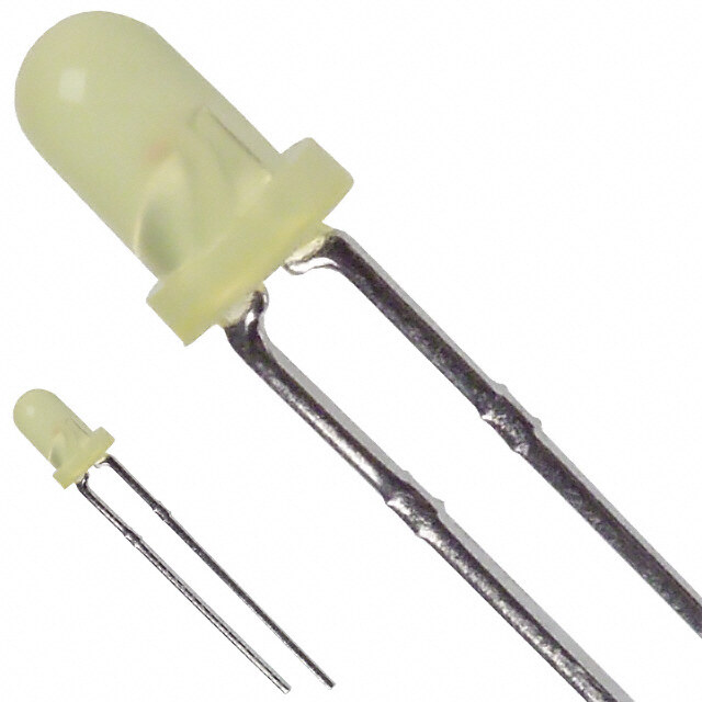
ICGOO在线商城 > 光电元件 > LED 指示 - 分立 > LNJ424C46RA
 Datasheet下载
- 型号: LNJ424C46RA
- 制造商: Panasonic Corporation
- 库位|库存: xxxx|xxxx
- 要求:
| 数量阶梯 | 香港交货 | 国内含税 |
| +xxxx | $xxxx | ¥xxxx |
查看当月历史价格
查看今年历史价格
LNJ424C46RA产品简介:
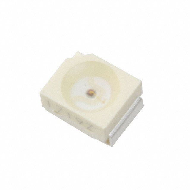
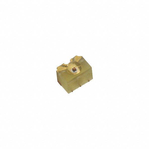
ICGOO电子元器件商城为您提供LNJ424C46RA由Panasonic Corporation设计生产,在icgoo商城现货销售,并且可以通过原厂、代理商等渠道进行代购。 LNJ424C46RA价格参考。Panasonic CorporationLNJ424C46RA封装/规格:LED 指示 - 分立, 琥珀色 589nm LED 指示 - 分立 2.1V 2-PLCC。您可以下载LNJ424C46RA参考资料、Datasheet数据手册功能说明书,资料中有LNJ424C46RA 详细功能的应用电路图电压和使用方法及教程。
Panasonic Electronic Components 旗下的型号 LNJ424C46RA,属于 LED 指示灯(分立式)产品。该 LED 主要用于各类电子设备中作为状态指示灯,具有高亮度、低功耗、长寿命等优点。

其典型应用场景包括:

1. 工业控制设备:如PLC、HMI、工业计算机等,用于显示设备运行状态、报警或通讯状态。
2. 家电产品:如洗衣机、冰箱、微波炉等家用电器,作为电源、功能状态或故障指示灯。
3. 通信设备:如路由器、交换机、基站设备等,用于指示网络连接、数据传输或电源状态。
4. 汽车电子系统:用于仪表盘、控制面板或车载设备中的状态显示。
5. 测试与测量仪器:如万用表、示波器等,用作功能指示或测量状态提示。

LNJ424C46RA 具备良好的环境适应性和稳定性,适用于需要可靠视觉反馈的多种电子系统中。
| 参数 | 数值 |
| 产品目录 | |
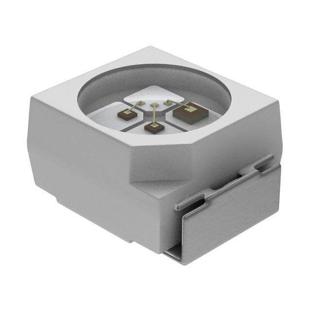
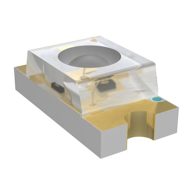
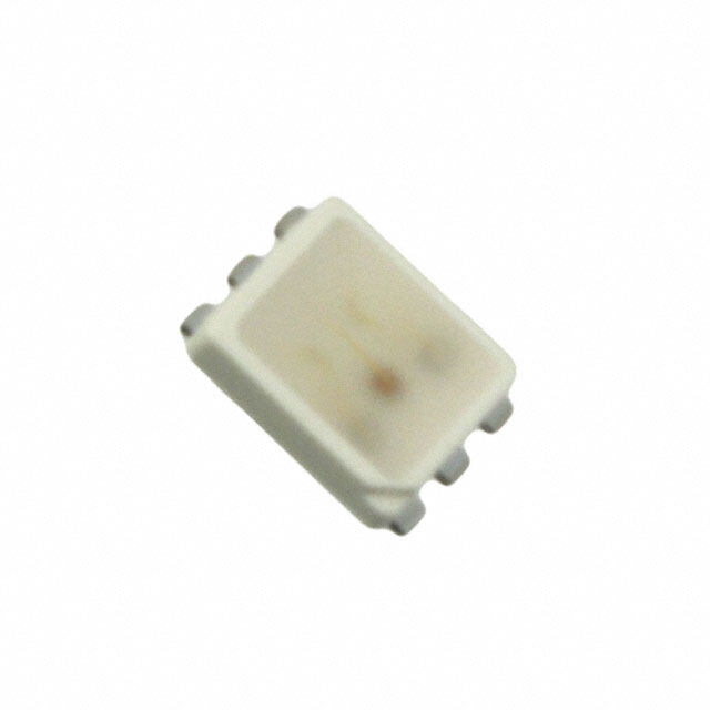
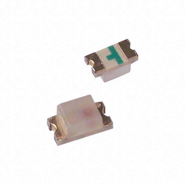
| 描述 | LED SMD AMBER 2-PLCC |
| 产品分类 | |
| 品牌 | Panasonic Electronic Components |
| 数据手册 | |
| 产品图片 | |
| 产品型号 | LNJ424C46RA |
| rohs | 无铅 / 符合限制有害物质指令(RoHS)规范要求 |
| 产品系列 | - |
| 其它名称 | LNJ424C46RATR |
| 包装 | 带卷 (TR) |
| 大小/尺寸 | 3.20mm 长 x 2.80mm 宽 |
| 安装类型 | 表面贴装 |
| 封装/外壳 | 2-PLCC |
| 标准包装 | 2,000 |
| 毫烛光等级 | 230mcd |
| 波长-主 | 589nm |
| 波长-峰值 | 595nm |
| 测试电流时的光通量 | - |
| 电压-正向(Vf)(典型值) | 2.1V |
| 电流-测试 | 20mA |
| 视角 | - |
| 透镜样式/尺寸 | 圆形,带平顶,2.4mm |
| 透镜类型 | - |
| 颜色 | 琥珀 |
| 高度 | 1.80mm |


- 商务部:美国ITC正式对集成电路等产品启动337调查
- 曝三星4nm工艺存在良率问题 高通将骁龙8 Gen1或转产台积电
- 太阳诱电将投资9.5亿元在常州建新厂生产MLCC 预计2023年完工
- 英特尔发布欧洲新工厂建设计划 深化IDM 2.0 战略
- 台积电先进制程称霸业界 有大客户加持明年业绩稳了
- 达到5530亿美元!SIA预计今年全球半导体销售额将创下新高
- 英特尔拟将自动驾驶子公司Mobileye上市 估值或超500亿美元
- 三星加码芯片和SET,合并消费电子和移动部门,撤换高东真等 CEO
- 三星电子宣布重大人事变动 还合并消费电子和移动部门
- 海关总署:前11个月进口集成电路产品价值2.52万亿元 增长14.8%

PDF Datasheet 数据手册内容提取
Regulations Total pages Page KG3F6694/K No. 13 1 Product Specification 3528 Package Size Type Chip LED Type Number:LNJ424C46RA Panasonic Unified Parts Number:LNJ424C46RA Semiconductor Company, Panasonic Corporation Established Applied Checked Prepared by by by by Y.Matsuyama T.Kitazono A.Nakano 2011-04-05 Established Revised Semiconductor Company, Panasonic Corporation
LNJ424C46RA Product Specification Total pages Page 13 2 Table of contents 1. Product Summary ・・・・・・・・・・・・・・・・・・・・・・・・・・・・・・・・・・・・・・・・・・・・・・・・・・・・・・・・・・・・ 3 2. Absolute Maximum Ratings ・・・・・・・・・・・・・・・・・・・・・・・・・・・・・・・・・・・・・・・・・・・・・・・・・・・ 3 3. Electrical-Optical Characteristics ・・・・・・・・・・・・・・・・・・・・・・・・・・・・・・・・・・・・・・・・・・・・・ 3 ~ 4 4. Typical characteristic(Reference) ・・・・・・・・・・・・・・・・・・・・・・・・・・・・・・・・・・・・・・・・・・・・・ 5 ~ 6 5. Outline ・・・・・・・・・・・・・・・・・・・・・・・・・・・・・・・・・・・・・・・・・・・・・・・・・・・・・・・・・・・・・・・・・・・・・・・ 7 6. Recommended Land Layout ・・・・・・・・・・・・・・・・・・・・・・・・・・・・・・・・・・・・・・・・・・・・・・・・・・ 7 7. Recommended Soldering Conditions ・・・・・・・・・・・・・・・・・・・・・・・・・・・・・・・・・・・・・・・・・ 8 ~ 9 8. Precautions for Application Design ・・・・・・・・・・・・・・・・・・・・・・・・・・・・・・・・・・・・・・・・・・・ 10 9. Handling Instructions ・・・・・・・・・・・・・・・・・・・・・・・・・・・・・・・・・・・・・・・・・・・・・・・・・・・・・・・・・ 11 ~ 12 10. Thermal Stress to Optical Device ・・・・・・・・・・・・・・・・・・・・・・・・・・・・・・・・・・・・・・・・・・・・・ 13 11. Guarantee ・・・・・・・・・・・・・・・・・・・・・・・・・・・・・・・・・・・・・・・・・・・・・・・・・・・・・・・・・・・・・・・・・・・ 13 12. Others ・・・・・・・・・・・・・・・・・・・・・・・・・・・・・・・・・・・・・・・・・・・・・・・・・・・・・・・・・・・・・・・・・・・・・・・ 13 《Attached paper》 1. Packing Specification ・・・・・・・・・・・・・・・・・・・・・・・・・・・・・・・・・・・・・・・・・・・・・・・・・・・・・・・・ 1 ~ 5 2. Reliability Test Result ・・・・・・・・・・・・・・・・・・・・・・・・・・・・・・・・・・・・・・・・・・・・・・・・・・・・・・・・ 1 2011-04-05 Established Revised Semiconductor Company, Panasonic Corporation
LNJ424C46RA Product Specification Total pages Page 13 3 ■ Product Summary Type Amber Light Emitting Diode (3528 Package size Type Chip LED) Application Indicators Material InGaAlP ■ Absolute Maximum Ratings Item Symbol Ratings Unit Remarks Power dissipation P 80 mW D Forward current I 30 mA F Pulse forward current I 90 mA (Note1) FP Reverse voltage V 4 V R Operating ambient Topr -40 ~ +100 ℃ temperature Storage temperature Tstg -40 ~ +100 ℃ (Note1) The condition of I is duty 10 %, pulse width 1 ms FP Please contact us for further information regarding special operating conditions such as I :less than DC =1 mA F I :less than pulse width =1 ms, duty=10 % FP ■ Electrical-Optical Characteristics (Ta=25 ℃±3 ℃) Item Symbol Condition Min. Typ. Max. Unit Luminous intensity I I =20 mA DC 140 230 380 mcd (Note2) O F Reverse current I V =4 V - - 100 μA R R Forward voltage V I =20 mA DC - 2.1 2.5 V F F Dominant emission λd I =20 mA DC 584 589 596 nm wavelength (Note3) F Peak emission wavelength λp I =20 mA DC - 595 - nm F Spectral half band width ⊿λ I =20 mA DC - 20 - nm F (Note2) Rank classification of luminous intensity. (Condition:I =20 mA DC) F Rank Luminous intensity Unit 1 140 ~ 200 2 200 ~ 270 mcd 3 270 ~ 380 ・Measurement tolerance is ±15 %. ・Luminous intensity standard is equal to NIST. (Note3) Rank classification of dominant emission wavelength. (Condition:I =20 mA DC) F Rank Dominant emission wavelength Unit L 584 ~ 590 nm H 590 ~ 596 ・Measurement tolerance is ±2 nm. 2011-04-05 Established Revised Semiconductor Company, Panasonic Corporation
LNJ424C46RA Product Specification Total pages Page 13 4 (Note4) Be careful about the product destruction by static electricity. (Note5) Precautions for circuit design of LED operation. (A) (B) The brightness difference is thought by the influence of VF about the circuit of (A) and avoids using, please. Recommend the use of the circuit of (B). 2011-04-05 Established Revised Semiconductor Company, Panasonic Corporation
LNJ424C46RA Product Specification Total pages Page 13 5 ■ Typical characteristic(Reference) Forward Current vs. Forward Voltage Relative Luminous Intensity vs. Ambient Temperature 100 1000 Ta=25 ℃ IF=20 mA ) % 50 ( o (mA) F 30 nsity : I nt : I Inte e s 100 urr 10 ou C n d mi r 5 u rwa e L Fo 3 ativ el R 1 10 1.0 1.5 2.0 2.5 3.0 3.5 -40 -20 0 20 40 60 80 100 Forward Voltage : V (V) Ambient Temperature : Ta (℃) F Luminous Intensity vs. Forward Current Forward Current vs. Ambient Temperature 10000 40 Ta=25 ℃ 35 d) mc 1000 A) 30 ( m O ( sity : I nt : I F 25 en 100 rre 20 s Int d Cu ou ar 15 n w umi 10 For 10 L 5 1 0 1 10 100 0 20 40 60 80 100 120 Ambient Temperature : T (℃) Forward Current : I (mA) a F ※The description data of this page is a typical value. 2011-04-05 Established Revised Semiconductor Company, Panasonic Corporation
LNJ424C46RA Product Specification Total pages Page 13 6 Relative Luminous Intensity - Wavelength Characteristics 120 %) 100 ( y nsit 80 e nt I us 60 o n mi u 40 L e v ati 20 el R 0 350 400 450 500 550 600 650 700 750 Wavelength (nm) Directive Characteristics Relative Luminous Intensity I (%) O ※The description data of this page is a typical value. 2011-04-05 Established Revised Panasonic Semiconductor Opto Devices Co., Ltd.
LNJ424C46RA Product Specification Total pages Page 13 7 ■ Outline Polarity Unit:mm 1 2 Anode Cathode Marking Position 3.5±0.2 3.2 φ2.4 1 2 C0.8 Marking Specification 5 5 0. 0.8 n ount of resiMax 0.00 Max 0.1 ±1.80.2 1 4 0 5 A m A 1 4 05 A □ 2 Reserve 2 1 2 0. Day Lot No. (A・B・C・・・) 2. ± 8 2. Day (01・02・03・・・) Month(1~9,O,N,D) Year (0~9) 0.8±0.2 0.8±0.2 Recommended Land Layout 4.5 (1.5) 1.5 (1.5) 1. Anode 2. Cathode 6 2. (Note1) Tolerance unless specified:±0.1 mm. (Note2) ( ) A size is a reference. 2011-04-05 Established Revised Semiconductor Company, Panasonic Corporation
LNJ424C46RA Product Specification Total pages Page 13 8 ■ Recommended Soldering Conditions 1. The reflow soldering 1) The first time reflow soldering Pleasa use it on condition that the folloeing. Max. 260 ℃ 250 ℃ Rate:1 ℃/s ~ 5 ℃/s 200 ℃ 150 ℃~ 180 ℃ Preheating Max.10 s 40 ℃ 30 s 120 s Max 70 s *This should be a profile on the print wiring board and FPC surface. 2) The second time reflow soldering (Up to the 2nd time) In case of the second time reflow, please store the product 10 ℃~30 ℃,60 %RH and proceed the reflow soldering within 3 days after the first time reflow. Follow the same condition as the first reflow. 2. Hand soldering 1) Basically keep the temperature on the edge of iron at 350 ℃ and apply within 3 s. If the temperature is higher than the condition above, apply in a shorter time (1 s per 10 ℃). 2) The iron equipped with temperature control circuit should be used. 3) Do not give a stress to lead or resin on soldering. Especially do not let iron contact with them. A LED chip will be damaged and broken by extreme stress. 4) Do not also give a stress to the device and bend of PC board adjusted right after manual soldering iron. 5) The LED which was removed from PC board should not be used again. 6) Please do not solder excluding the reflow soldering or the manual soldering Iron. 2011-04-05 Established Revised Semiconductor Company, Panasonic Corporation
LNJ424C46RA Product Specification Total pages Page 13 9 3. Automatic Mounting These products are available for automatic mounting machines. However, concerning demand on structure and performance of these devices, you should pay attentions to the followings below. 1) Though we’ve performed anti-static operation on these devices, static electricity can be frequently occurred in dry atmosphere and cause products to stick on the cover tapes. Please study to control humidity and to perform anti-static measure. 2) If a successful mounting is not secured on your systems, you may study the following subjects. Especially for a round shaped tool, please choose the one not Inside diameter of tool sticking out from the LED’s lens area. For a particular tool (“asterisk” type etc.), which intends to Shape of tool incline due to its shape. Please study the location and the size of it. Please set the height of the tool a little lower from top of the Height of tool face of tape guide. Please adjust the absorb position as a center of device as Position in absorption possible. To reduce the vibration on mounting, please discuss taking Vibration in mounting necessary measures against optimization of mounting speed and tensions in winding and feeding tapes. Mind the pin position of the products prepared a pin-hole (byφ0.5 mm) on the bottom of the embossed tape. Pin push up system “Pin push up system” is suitable only for products with a pin-hole but not for others. 2011-04-05 Established Revised Semiconductor Company, Panasonic Corporation
LNJ424C46RA Product Specification Total pages Page 13 10 ■ Precautions for Application Design 1. Connect the current control resistor in the circuit and operate products within rated range of use. 2. Avoid instant reverse voltage (over current) when turning ON/OFF the circuit. 3. Check a pattern dimension well before use. 4. Avoid using under environments as shown in the following. ・A place where dust or corrosive gas is generated. ・A place where dew drop is generated on the product surface (LED). 5. Avoid circuit design that the product (LED) can be heated by adjacent high power electrical heating element such as high power resistor or by high component density. 6. Mount the chip at right angles to the longitudinal direction of the PC board so that the stress on the product should be decreased. (Notes) We recommend the LED be placed on the PC board as shown in diagram A. If the LED must be placed on the PC board as shown in diagram B, special care should be taken to insure that the LED is not affected by bend of the PC board after the soldering process. (LED arrangement on PC board) (A) (B) 2011-04-05 Established Revised Semiconductor Company, Panasonic Corporation
LNJ424C46RA Product Specification Total pages Page 13 11 ■ Handling Instructions 1. Storage In order to avoid absorption of moisture during conveyance and storage of products, we are applying moisture-proof packaging by means of aluminum-laminated bags containing silica gel. Then, when absorption of moisture proceeds, the color of indicators in the silica gel changes, to which must be paid much attention. After the aluminum-laminated bag is opened, absorption of moisture of the products proceeds quickly, which is likely to cause characteristic defects due to thermal stress generated during the re-flowing process in the worst case. Therefore when these products are used, be sure to open the bags one by one to complete re-flowing quickly. LED terminals, as being treated with Ag plating, may be changed in the surface quality and degraded in solderability when exposed to the following conditions. Therefore, pay enough attention to the storage condition. 2. Conditions and Terms of Storage of Products Please store products according to the following product conditions depending on the conditions of the products. Conditions of Storage Conditions of Product Ambient Temperature Term Temperature humidity When aluminum-laminated 10 ℃ ~ 30 ℃ 60 % or under Within one year bag is not opened yet When aluminum-laminated 10 ℃ ~ 30 ℃ 60 % or under Within 3 days bag is opened Up to the second time after 10 ℃ ~ 30 ℃ 60 % or under Within 3 days the first reflowing If the above-mentioned treatment was not made (including a case of discoloration of the silica gel indicator in the bag or similar), remove moisture by means of baking treatment or the like before use. 《Recommended Baking Conditions》 In a reel condition (as taken out of the aluminum-laminate bag) Temperature:60 ℃. Time: More than 12 h and up to 24 h. (However, the baking treatment is limited to one time only.) (Note) ・The poor characteristic may generate on the products when a great deal of neglect time after the opening in your process. Also under the products with taping, there is a possibility that the strength of cover tape peeling fluctuates and the mounting error occurs after baking. Therefore, please take sufficient advance checks and control in your process. Meanwhile, please note that we are not responsible for the problem occurred except in the condition above. 3. Washing 1) Do not wash the products in principle. 2) If washing is required by a reason of the set, be sure to make it after the products are mounted (after reflowing) according to the following conditions. ・Alcohol is recommended for cleaning. Do not use a chlorine solvent, which may cause damage to the epoxy and product and deterioration of the products. ・As for ultrasonic cleaning, it may differently affect each of the mounting board, such as resonance. Sufficient checks on the ultrasonic cleaning is required for actual use. ・Avoid the use of brushing because it sometime damages light-emitting surfaces. 2011-04-05 Established Revised Semiconductor Company, Panasonic Corporation
LNJ424C46RA Product Specification Total pages Page 13 12 4. Product strength Resin is used as sealing material for light emitting diode on this product. The molding resin may be peeled off with strong direct shocks in the resin part by reducing strength of the resin after heating. So you should pay attention to keep products from shocking on resin side, especially during soldering process and using soldering irons. And after soldering process, please avoid shocking directly on resin side, such as in the following cases, handling PCB’s, piling them up and putting them in magazines. Especially small type chip LEDs should be carefully handled. 5. Static electricity This LED is sensitive to static electricity and care should be fully taken in handing it. In the event that the voltage greater than absolute maximum rating is applied, which will damage LEDs. Please take necessary measures against Static electricity and serge in building LED assembly line and in handling LED in mid-flow of the process. *Please take the following measures such that the voltage and surge voltage more than an element resisting pressure level will not be applied. 1) Check the entire drive circuit including the power source. As a check example, a surge current generated at power-on/off should be checked not to exceed the absolute maximum ratings of the LED. Please also insert an appropriate protective circuit into the LED driver circuit. ・As shown in the figure, in order to protect LED, it is recommended to use a Zener diode. 2) Beware of destruction by static electricity in handling LEDs. As proactive measures against static electricity, it is effective to earth your body (via 1 MΩ), spread conductive mat on the floor, wear semi conductive work uniform and shoes and use semi conductive containers. Also, be sure to earth the nose of a soldering iron. It is recommended to use an ionizor in the facility or the environment where static electricity may be generated easily. 2011-04-05 Established Revised Semiconductor Company, Panasonic Corporation
LNJ424C46RA Product Specification Total pages Page 13 13 ■ Thermal Stress to Optical Device Since light transmissivity is important for the package resin of optical devices (LED’s, photodiodes, photo ICs, Photosensors, photocouplers), it is necessary for resin to contain additives in it. For this reason, it has a lower thermal deformation temperature, compared with the package resin for ICs, LSI’s and so on and is in the vicinity of the maximum storage temperature. Unless it is designed under the operating conditions, taking into an operating current and ambient conditions into account, the optical devices may be destroyed due to thermal stress caused to the operating optical devices and this may cause lower light output and disconnection. ■ Guarantee The warranty will be valid only within the reliability test results or the items and terms of the reliability assurance standard. It is also limited to that of the delivered product itself and we are not responsible for the labor cost for replacement work, compensation for loss and the like. The following cases are onerous since they are out of our guarantee even during the guarantee period: ・Troubles resulting from careless handling or erroneous use. ・Troubles resulting from unreasonable repair or improvement. ・Troubles resulting from irresistible force such as natural disasters. Should there be any doubt, we will verify it to clarify the cause in the presence of both parties in principle and take a proper action. ■ Others 1) For matters on quality agreed between you and as those mentioned in these delivery specifications only are valid basically and matters decided between you and us before the receipt of these specifications become invalid unless they are mentioned in these specifications. But, if any inadequacy is present, we are ready for a discussion with you to settle the matter. In case any modification is required after the receipt of those specifications, only matters agreed by you and us are valid. 2) For a special application or question, contact us before the fact and without delay. 3) Though we will deliver the products for which we guarantee the matters on quality mentioned in these specifications, please investigate on your side the incorporation into actual sets, duration under actual working conditions and other matters on quality of the products sufficiently. 4) If these delivery specifications are not returned to us within two weeks after the issue, we regard them as received, which please understand. 5) For the doubts or necessity of change in this specification, mutual discussion will be made for the solution 6) The specifications will be changed after prior discussion. 7) UL Standard UL standard is not acquired since optical characteristics of sillicon resin is superior. 8) This product is RoHS-free supported. 2011-04-05 Established Revised Semiconductor Company, Panasonic Corporation
LNJ424C46RA Packing Specification Total pages Page 5 1 ■ Embossed taping specifications Unit:mm φ1.5 +0.1 -0 1 0. ± 4.0±0.1 2.0±0.05 5 0.3±0.05 7 1. 0.2 ±0.05 +0.3 0 -0.1 3.5 8. ±0.1 ±0.1 5) 3.9 3.75 7 2. ( 4.0±0.1 φ1.05±0.05 2.2±0.1 3.05±0.1 2 2.95±0.1 0. (Note1) Unless specified R of the corner is Max. 0.3 mm. (Note2) Allowance of accumulated pitch of feeding holes is ±0.2 mm per 10 pitches. (Note3) Tolerance unless specified is ±0.1 mm. 2011-04-05 Established Revised Semiconductor Company, Panasonic Corporation
LNJ424C46RA Packing Specification Total pages Page 5 2 ■ Reel Specification Unit:mm +0 φ180.0 -3.0 2.0±0.2 A-A’SECT φ13.0±0.2 3 0 +1.0 0. 1. φ60.0 -0 ± ± 0 4 9. 1. 1 (Note1) This part is the application of JEITA ETX-7001. 2011-04-05 Established Revised Semiconductor Company, Panasonic Corporation
LNJ424C46RA Packing Specification Total pages Page 5 3 ■ Taping specifications Blank (Trailer part) Product (LED enclosure part) Blank (start) Leader Min. 40 mm Min. 40 mm Min. 200 mm Mounting part Pulling direction Pin-feed hole side Outline Polarity mark EIAJ C3 label 1. Pin-feed holes should be on the left side on the tape in the pulling direction. 2. Chip LED taping direction. Refer to the above Figure. 3. The leader part is saved as cover tape, which should be 200 mm or longer. 4. Keep more than 10 emboss blanks both at front and end of the taping. ■ Mechanical strength and treatment F Cover tape 10 ° Carrier tape Tape feeding direction 1. Exfoliation strength of the cover tape should be 0.2 N ~ 0.7 N. 2. Tape bending strength Tape should not be deformed by bending with a radius of 15 mm. 3. Percentage defective of enclosed The product which was enclosed in reverse direction or with back side up should be counted as 0 piece/reel. The number of dropped parts should be 0.1 % of entire number of parts or 1 piece, whichever larger. There should be no continuous dropping however total number has to remain intact. 4. There should be no tape joint. 2011-04-05 Established Revised Semiconductor Company, Panasonic Corporation
LNJ424C46RA Packing Specification Total pages Page 5 4 ■ Packing form 1. A reel of 2 000 LED’s is a basic unit. 2. A reel and silica gel are put into an aluminum lamination bag. Reel packing Aluminum lamination bag packing Notice label (Printing) back Reel EIAJ C3 label ※Rank can not be mixed within a reel. Aluminum lamination bag Silica gel Packing case (Inner) Packing case (Outer) Notice label EIAJ C3 label ※Rank can be mixed within a packing (inner box and outer box). EIAJ C3 label ※Fractional packing, I,e, tape & reel and inner or outer carton, can be happened. (Note) Please refer the product traceability with date code on the packing label. 2011-04-05 Established Revised Semiconductor Company, Panasonic Corporation
LNJ424C46RA Packing Specification Total pages Page 5 5 ■ Internal use Label Items 1. Packing Classification 1) Reel : 2 000 pcs 2) Packing (Inner) : 6 000 pcs 3) Packing (outer) : 12 000 pcs 2. Label 1) EIAJ C3 labeling F A H B I C D G E A : Customer code B : Internal packing code C : Rank D : Date code Example of date code (Reference) 14 ⇒ April, 2011 January February ………………… October November December 1 2 ………………… O N D (October November December) *Only on the packing case tight number can be contained. E : Date of label printing F : Quantity G : Product number H : Bar code symbol I : Pb free ※ Product name indication (Example) LNJ424C46 RA Taping specification Chip LED product № 2) Indication method (Notice label) 2011-04-05 Established Revised Semiconductor Company, Panasonic Corporation
LNJ424C46RA Reliability Test Result Total pages Page 1 1 Issued by Reaffirmed by Product Name : LNJ424C46RA Panasonic Semiconductor Opto Devices Co., Ltd. Quality control group ◆Reliability Assurance Criterion(MIL-STD-19500H LTPD 15 %) Judgment Test items Test conditions Test results criteria Consecutive operating I Max., Ta=25 ℃, t=1 000 h 0/15 B life test FDC High temperature Tstg Max., t=1 000 h 0/15 A storage test Low temperature Tstg Min., t=1 000 h 0/15 A storage test High temperature Ta=60 ℃, RH≧90 %, t=1 000 h 0/15 A humidity storage test Temperature:Ta=250 ℃, t=10 s Max., Max. 260 ℃ Reflow soldering Soldering heat test 0/15 A Refer to attached paper product specification Sheet No.13/7. Temperature: Temperature cycle test 【Tstg Min.~25 ℃~Tstg Max.~25 ℃】 0/15 A (gaseous phase) Time: (30 min 5 min 30 min 5 min) × 20 cycles Temperature:【Tstg Max. ~ 0 ℃】 Thermal shock test Time : (5 min 5 min) 0/15 A (liquid phase) × 10 cycles Drop distance : 1 m Fall test Drop the device 3 times on a maple board of 3 cm or 0/15 A more in thickness. ◆Judgment Criteria A Item Symbol Measurement condition Limit Unit Forward Voltage V Same as the Product Standards Upper Limit×1.2 V F Reverse Leakage I Same as the Product Standards Upper Limit×2.0 μA Current R Luminous Intensity ⊿I Same as the Product Standards Lower Limit×0.7 % O ◆Judgment Criteria B Item Symbol Measurement condition Limit Unit Forward Voltage V Same as the Product Standards Upper Limit×1.2 V F Reverse Leakage I Same as the Product Standards Upper Limit×2.0 μA Current R Luminous Intensity ⊿I Same as the Product Standards Lower Limit×0.5 % O (Notes) If you have any special requirement, please inquire for us. 2011-04-05 Established Revised Semiconductor Company, Panasonic Corporation
LNJ424C46RA Product Specification Total pages Page Standard Revision History 1 1 Date Page Contents of revision Revision reason 2011-04-05 ・Novel enactment 2011-04-05 Established Revised Semiconductor Company, Panasonic Corporation