ICGOO在线商城 > 集成电路(IC) > 时钟/计时 - 时钟发生器,PLL,频率合成器 > LMX2541SQ3320E/NOPB

 Datasheet下载
- 型号: LMX2541SQ3320E/NOPB
- 制造商: Texas Instruments
- 库位|库存: xxxx|xxxx
- 要求:
| 数量阶梯 | 香港交货 | 国内含税 |
| +xxxx | $xxxx | ¥xxxx |
查看当月历史价格
查看今年历史价格
LMX2541SQ3320E/NOPB产品简介:
ICGOO电子元器件商城为您提供LMX2541SQ3320E/NOPB由Texas Instruments设计生产,在icgoo商城现货销售,并且可以通过原厂、代理商等渠道进行代购。 LMX2541SQ3320E/NOPB价格参考。Texas InstrumentsLMX2541SQ3320E/NOPB封装/规格:时钟/计时 - 时钟发生器,PLL,频率合成器, 。您可以下载LMX2541SQ3320E/NOPB参考资料、Datasheet数据手册功能说明书,资料中有LMX2541SQ3320E/NOPB 详细功能的应用电路图电压和使用方法及教程。
LMX2541SQ3320E/NOPB是德州仪器(Texas Instruments)推出的一款高性能低相位噪声射频时钟发生器,属于时钟/计时类中的PLL(锁相环)和频率合成器产品。该芯片集成了Delta-Sigma调制分数-N PLL和压控振荡器(VCO),支持宽频率输出范围,适用于需要高精度、低抖动时钟信号的射频和通信系统。

其典型应用场景包括:无线通信基础设施(如基站和微波回传系统)、测试与测量设备(如频谱分析仪、信号发生器)、软件定义无线电(SDR)、雷达系统以及高速数据转换器(ADC/DAC)的采样时钟同步。此外,该器件也广泛用于需要多频段本地振荡信号生成的系统中,提供稳定且可编程的高频时钟输出。

LMX2541SQ3320E/NOPB采用小型化QFN封装,具备良好的电源噪声抑制能力和灵活的配置选项,可通过SPI接口进行参数设置,便于系统集成与调试。其“NOPB”后缀表示无铅环保设计,符合RoHS标准,适用于对可靠性和环境要求较高的工业及通信应用。
| 参数 | 数值 |
| 产品目录 | 集成电路 (IC)半导体 |
| 描述 | IC PLL FREQ SYNTH W/VCO 36LLP锁相环 - PLL Ultra-Lo Noise PLLatinum Freq Synth |
| 产品分类 | |
| 品牌 | Texas Instruments |
| 产品手册 | http://www.ti.com/lit/gpn/lmx2541 |
| 产品图片 |
|
| rohs | 符合RoHS无铅 / 符合限制有害物质指令(RoHS)规范要求 |
| 产品系列 | RF集成电路,锁相环 - PLL,Texas Instruments LMX2541SQ3320E/NOPB- |
| 数据手册 | |
| 产品型号 | LMX2541SQ3320E/NOPB |
| PLL | 是 |
| 产品种类 | 锁相环 - PLL |
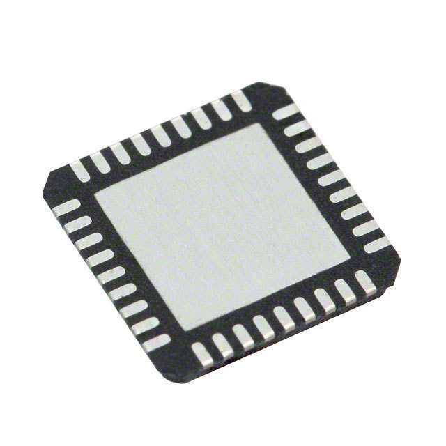
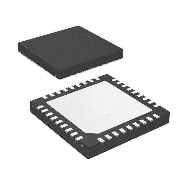
| 供应商器件封装 | 36-WQFN (6x6) |
| 其它名称 | *LMX2541SQ3320E/NOPB |
| 分频器/倍频器 | 是/是 |
| 包装 | 剪切带 (CT) |
| 商标 | Texas Instruments |
| 安装类型 | 表面贴装 |
| 安装风格 | SMD/SMT |
| 封装 | Reel |
| 封装/外壳 | 36-WFQFN 裸露焊盘 |
| 封装/箱体 | LLP EP |
| 工作温度 | -40°C ~ 85°C |
| 工作电源电压 | 3.3 V |
| 工厂包装数量 | 1000 |
| 差分-输入:输出 | 无/无 |
| 最大工作温度 | + 85 C |
| 最大输入频率 | 6000 MHz |
| 最小工作温度 | - 40 C |
| 最小输入频率 | 5 MHz |
| 标准包装 | 1 |
| 比率-输入:输出 | 2:2 |
| 电压-电源 | 3.15 V ~ 3.45 V |
| 电源电压-最大 | 3.45 V |
| 电源电压-最小 | 3.15 V |
| 电路数 | 1 |
| 电路数量 | 1 |
| 类型 | 时钟/频率合成器,RF |
| 系列 | LMX2541 |
| 输入 | 时钟 |
| 输出 | 时钟 |
| 频率-最大值 | 3.6GHz |


- 商务部:美国ITC正式对集成电路等产品启动337调查
- 曝三星4nm工艺存在良率问题 高通将骁龙8 Gen1或转产台积电
- 太阳诱电将投资9.5亿元在常州建新厂生产MLCC 预计2023年完工
- 英特尔发布欧洲新工厂建设计划 深化IDM 2.0 战略
- 台积电先进制程称霸业界 有大客户加持明年业绩稳了
- 达到5530亿美元!SIA预计今年全球半导体销售额将创下新高
- 英特尔拟将自动驾驶子公司Mobileye上市 估值或超500亿美元
- 三星加码芯片和SET,合并消费电子和移动部门,撤换高东真等 CEO
- 三星电子宣布重大人事变动 还合并消费电子和移动部门
- 海关总署:前11个月进口集成电路产品价值2.52万亿元 增长14.8%


PDF Datasheet 数据手册内容提取
Product Sample & Technical Tools & Support & Folder Buy Documents Software Community LMX2541 SNOSB31J–JULY2009–REVISEDDECEMBER2014 LMX2541 Ultra-Low Noise PLLatinum Frequency Synthesizer With Integrated VCO 1 Features 3 Description • MultipleFrequencyOptionsAvailable The LMX2541 device is an ultra low-noise frequency 1 synthesizer which integrates a high-performance (SeeDeviceComparisonTable) delta-sigma fractional N PLL, a VCO with fully • FrequenciesFrom31.6MHzto4000MHz integrated tank circuit, and an optional frequency • VeryLowRMSNoiseandSpurs divider. The PLL offers an unprecedented normalized • –225dBc/HzNormalizedPLLPhaseNoise noise floor of –225 dBc/Hz and can be operated with up to 104 MHz of phase-detector rate (comparison • IntegratedRMSNoise(100Hzto20MHz) frequency) in both integer and fractional modes. The – 2mRad(100Hzto20MHz)at2.1GHz PLL can also be configured to work with an external – 3.5mRad(100Hzto20MHz)at3.5GHz VCO. • UltraLow-NoiseIntegratedVCO The LMX2541 integrates several low-noise, high- • ExternalVCOOption(InternalVCOBypassed) precisionLDOsandoutputdrivermatchingnetworkto provide higher supply noise immunity and more • VCOFrequencyDivider1to63(AllValues) consistent performance, while reducing the number of • ProgrammableOutputPower external components. When combined with a high- • Upto104-MHzPhaseDetectorFrequency quality reference oscillator, the LMX2541 generates a verystable,ultralow-noisesignal. • IntegratedLow-NoiseLDOs • ProgrammableChargePumpOutput The LMX2541 is offered in a family of 6 devices with varying VCO frequency range from 1990 MHz up to 4 • PartiallyIntegratedLoopFilter GHz. Using a flexible divider, the LMX2541 can • DigitalFrequencyShiftKeying(FSK)Modulation generatefrequenciesaslowas31.6MHz. Pin The LMX2541 is a monolithic integrated circuit, • IntegratedReferenceCrystalOscillatorCircuit fabricated in a proprietary BiCMOS process. Device • HardwareandSoftwarePowerDown programming is facilitated using a three-wire • FastLockModeandVCO-BasedCycleSlip MICROWIRE interface that can operate down to 1.6 Reduction volts. Supply voltage ranges from 3.15 V to 3.45 V. The LMX2541 is available in a 36-pin 6-mm × 6-mm • AnalogandDigitalLockDetect ×0.8-mmWQFNpackage. • 1.6-VLogicCompatibility DeviceInformation(1) 2 Applications VCOFREQUENCY PARTNUMBER PACKAGE (MHz) • WirelessInfrastructure(UMTS,LTE,WiMax) LMX2541SQ2060E WQFN(36) 1990-2240 • BroadbandWireless LMX2541SQ2380E WQFN(36) 2200-2530 • WirelessMeterReading LMX2541SQ2690E WQFN(36) 2490-2865 • TestandMeasurement LMX2541SQ3030E WQFN(36) 2810-3230 • FMMobileRadio LMX2541SQ3320E WQFN(36) 3130-3600 space LMX2541SQ3740E WQFN(36) 3480-4000 (1) For all available packages, see the orderable addendum at theendofthedatasheet. SystemBlockDiagram Clean Ultra-Clean Dirty Input Reference Local Oscillator Clock Clock PLL Dist. PLL LMK04000 LMX2541 (Clock Jitter Cleaner) (RF Synthesizer) 1 An IMPORTANT NOTICE at the end of this data sheet addresses availability, warranty, changes, use in safety-critical applications, intellectualpropertymattersandotherimportantdisclaimers.PRODUCTIONDATA.
LMX2541 SNOSB31J–JULY2009–REVISEDDECEMBER2014 www.ti.com Table of Contents 1 Features.................................................................. 1 9.2 FunctionalBlockDiagrams.....................................25 2 Applications........................................................... 1 9.3 FeatureDescription.................................................26 3 Description............................................................. 1 9.4 DeviceFunctionalModes........................................36 9.5 Programming...........................................................37 4 RevisionHistory..................................................... 2 9.6 RegisterMaps.........................................................38 5 DeviceComparisonTable..................................... 3 10 ApplicationandImplementation........................ 51 6 PinConfigurationandFunctions......................... 4 10.1 ApplicationInformation..........................................51 7 Specifications......................................................... 6 10.2 TypicalApplication ...............................................59 7.1 AbsoluteMaximumRatings......................................6 11 PowerSupplyRecommendations..................... 61 7.2 ESDRatings..............................................................6 12 Layout................................................................... 62 7.3 RecommendedOperatingConditions.......................6 12.1 LayoutGuidelines.................................................62 7.4 ThermalInformation..................................................6 12.2 LayoutExample....................................................63 7.5 ElectricalCharacteristics...........................................7 13 DeviceandDocumentationSupport................. 64 7.6 TimingRequirements..............................................11 7.7 TypicalCharacteristics............................................12 13.1 DeviceSupport......................................................64 13.2 Trademarks...........................................................64 8 ParameterMeasurementInformation................23 13.3 ElectrostaticDischargeCaution............................64 8.1 BenchTestSetups..................................................23 13.4 Glossary................................................................64 9 DetailedDescription............................................ 25 14 Mechanical,Packaging,andOrderable 9.1 Overview.................................................................25 Information........................................................... 64 4 Revision History ChangesfromRevisionI(February2013)toRevisionJ Page • AddedESDRatingstable,FeatureDescriptionsection,DeviceFunctionalModes,ApplicationandImplementation section,PowerSupplyRecommendationssection,Layoutsection,DeviceandDocumentationSupportsection,and Mechanical,Packaging,andOrderableInformationsection.................................................................................................. 1 ChangesfromRevisionH(February2013)toRevisionI Page • ChangedlayoutofNationalDataSheettoTIformat........................................................................................................... 36 2 SubmitDocumentationFeedback Copyright©2009–2014,TexasInstrumentsIncorporated ProductFolderLinks:LMX2541
LMX2541 www.ti.com SNOSB31J–JULY2009–REVISEDDECEMBER2014 5 Device Comparison Table VCO LMX2541SQ2060E LMX2541SQ2380E LMX2541SQ2690E LMX2541SQ3030E LMX2541SQ3320E LMX2541SQ3740E _DIV Fmin Fmax Fmin Fmax Fmin Fmax Fmin Fmax Fmin Fmax Fmin Fmax 1 1990.0 2240.0 2200.0 2530.0 2490.0 2865.0 2810.0 3230.0 3130.0 3600.0 3480.0 4000.0 2 995.0 1120.0 1100.0 1265.0 1245.0 1432.5 1405.0 1615.0 1565.0 1800.0 1740.0 2000.0 3 663.3 746.7 733.3 843.3 830.0 955.0 936.7 1076.7 1043.3 1200.0 1160.0 1333.3 4 497.5 560.0 550.0 632.5 622.5 716.3 702.5 807.5 782.5 900.0 870.0 1000.0 5 398.0 448.0 440.0 506.0 498.0 573.0 562.0 646.0 626.0 720.0 696.0 800.0 6 331.7 373.3 366.7 421.7 415.0 477.5 468.3 538.3 521.7 600.0 580.0 666.7 7 284.3 320.0 314.3 361.4 355.7 409.3 401.4 461.4 447.1 514.3 497.1 571.4 8 248.8 280.0 275.0 316.3 311.3 358.1 351.3 403.8 391.3 450.0 435.0 500.0 ... ... ... ... ... ... ... ... ... ... ... ... ... 63 31.6 35.6 34.9 40.2 39.5 45.5 44.6 51.3 49.7 57.1 55.2 63.5 All devices have continuous frequency coverage below a divide value of 8 (7 for most devices) down to their minimum frequency achievable with divide by 63. The numbers in bold show the upper end of this minimum continuous frequency range. For instance, the LMX2541SQ3740E option offers continuous frequency coverage from 55.2 MHz to 571.4 MHz and LMX2541SQ2060E offers continuous frequency coverage from 31.6 MHz to 280 MHz. If using the part in External VCO mode, all parts have roughly the same performance and any option willdo. Copyright©2009–2014,TexasInstrumentsIncorporated SubmitDocumentationFeedback 3 ProductFolderLinks:LMX2541
LMX2541 SNOSB31J–JULY2009–REVISEDDECEMBER2014 www.ti.com 6 Pin Configuration and Functions NJKPackage 36-PinWQFN TopView RFout NC LE CLK DATA VccDiv Bypass VccBias VccDig 36 35 34 33 32 31 30 29 28 GND 1 27 GND VregRFout 2 26 VregFRAC VccRFout 3 25 VccFRAC L1 4 24 RFoutEN 0 Lmid 5 GND 23 VccOSCin L2 6 22 OSCin* VccVCO 7 21 OSCin VregVCO 8 20 Ftest/LD VrefVCO 9 19 VccPLL2 10 11 12 13 14 15 16 17 18 GND CE ExtVCOin VccPLL1 VccCP1 Vtune CPout FLout VccCP2 PinFunctions PIN TYPE DESCRIPTION NAME NO. Bypass 30 Bypass PutacaptotheVccBiaspin. ChipEnable. CE 11 CMOS Thedeviceneedstobeprogrammedforthispintoproperlypowerdownthedevice. MICROWIREclockinput.HighimpedanceCMOSinput. CLK 33 High-ZInput ThispinisusedforthedigitalFSKmodulationfeature. CPout 16 Output Chargepumpoutput. DATA 32 High-ZInput MICROWIREserialdatainput.HighimpedanceCMOSinput. OptionalinputforusewithanexternalVCO. ExtVCOin 12 RFInput ThispinshouldbeACcoupledifusedorleftopenifnotused. FLout 17 Output Fastlockoutput. SoftwarecontrollablemultiplexedCMOSoutput. Ftest/LD 20 Output CanbeusedtomonitorPLLlockcondition. GND 0 GND TheDAPpadmustbegrounded. GND 1 GND GND 10 GND GND 27 GND L1 4 NC Donotconnectthispin. L2 6 NC Donotconnectthispin. LE 34 High-ZInput MICROWIRELatchEnableinput.HighimpedanceCMOSinput. Lmid 5 NC Donotconnectthispin. NC 35 NC Noconnect. Oscillatorinputsignal.Ifnotbeingusedwithanexternalcrystal,thisinputshouldbeAC OSCin 21 High-ZInput coupled. 4 SubmitDocumentationFeedback Copyright©2009–2014,TexasInstrumentsIncorporated ProductFolderLinks:LMX2541
LMX2541 www.ti.com SNOSB31J–JULY2009–REVISEDDECEMBER2014 PinFunctions(continued) PIN TYPE DESCRIPTION NAME NO. Complementaryoscillatorinputsignal.Canalsobeusedwithanexternalcrystal.Ifnot OSCin* 22 High-ZInput beingusedwithanexternalcrystal,thisinputshouldbeACcoupled. RFout 36 RFOutput RFoutput.MustbeACcoupledifused. RFoutEN 24 Input Softwareprogrammableoutputenablepin. VccBias 29 Supply SupplyforBiascircuitrythatisforthewholechip. VccCP1 14 Supply PowersupplyforPLLchargepump. VccCP2 18 Supply PowersupplyforPLLchargepump. VccDig 28 Supply Supplyfordigitalcircuitry,suchtheMICROWIRE. VccDiv 31 Supply Supplyfortheoutputdivider Supply VccFRAC 25 PowerSupplyforthePLLfractionalcircuitry. (LDOInput) VccOSCin 23 Supply SupplyfortheOSCinbuffer. VccPLL1 13 Supply PowersupplyforPLL. VccPLL2 19 Supply PowersupplyforPLL. Supply VccRFout 3 SupplyfortheRFoutputbuffer. (LDOInput) Supply VccVCO 7 SupplyfortheVCO. (LDOInput) VregFRAC 26 LDOOutput Regulatedpowersupplyusedforthefractionaldelta-sigmacircuitry. VregRFout 2 LDOOutput LDOOutputforRFoutputbuffer. VrefVCO 9 LDOBypass LDOBypass VregVCO 8 LDOOutput LDOOutputforVCO Vtune 15 High-ZInput TuningvoltageinputtotheVCO. Copyright©2009–2014,TexasInstrumentsIncorporated SubmitDocumentationFeedback 5 ProductFolderLinks:LMX2541
LMX2541 SNOSB31J–JULY2009–REVISEDDECEMBER2014 www.ti.com 7 Specifications 7.1 Absolute Maximum Ratings overoperatingfree-airtemperaturerange(unlessotherwisenoted) (1)(2) MIN MAX UNIT Vcc PowerSupplyVoltage –0.3 3.6 V V InputVoltagetopinsotherthanVccPins –0.3 (Vcc+0.3) V IN (3) T LeadTemperature(solder4sec.) 260 °C L T StorageTemperature –65 150 °C stg (1) StressesbeyondthoselistedunderAbsoluteMaximumRatingsmaycausepermanentdamagetothedevice.Thesearestressratings only,whichdonotimplyfunctionaloperationofthedeviceattheseoranyotherconditionsbeyondthoseindicatedunderRecommended OperatingConditions.Exposuretoabsolute-maximum-ratedconditionsforextendedperiodsmayaffectdevicereliability. (2) IfMilitary/Aerospacespecifieddevicesarerequired,pleasecontacttheTexasInstrumentsSalesOffice/Distributorsforavailabilityand specifications. (3) Nevertoexceed3.6V. 7.2 ESD Ratings VALUE UNIT Humanbodymodel(HBM),perANSI/ESDA/JEDECJS-001(1) ±2500 Charged-devicemodel(CDM),perJEDECspecificationJESD22- ±1750 V(ESD) Electrostaticdischarge C101(2) V Machinemodel(MM) ±400 (1) JEDECdocumentJEP155statesthat500-VHBMallowssafemanufacturingwithastandardESDcontrolprocess. (2) JEDECdocumentJEP157statesthat250-VCDMallowssafemanufacturingwithastandardESDcontrolprocess. 7.3 Recommended Operating Conditions MIN NOM MAX UNIT Vcc PowerSupplyVoltage(AllVccPins) 3.15 3.3 3.45 V T AmbientTemperature –40 85 °C A 7.4 Thermal Information LMX2541 LMX2541 LMX2541 SQ2060E SQ2060E SQ2060E THERMALMETRIC(1) UNIT 9Thermal 13Thermal 16Thermal Vias(2) Vias(3) Vias(4) R Junction-to-ambientthermalresistance 31.7 30.3 29.8 θJA °C/W ψ Junction-to-topcharacterizationparameter 7.3 7.3 7.3 JT (1) Formoreinformationabouttraditionalandnewthermalmetrics,seetheICPackageThermalMetricsapplicationreport,SPRA953. (2) RecommendedforMostReliableSolderability. (3) CompromiseBetweenSolderability,HeatDissipation,andFractionalSpurs. (4) RecommendedforOptimalHeatDissipationandFractionalSpurs. 6 SubmitDocumentationFeedback Copyright©2009–2014,TexasInstrumentsIncorporated ProductFolderLinks:LMX2541
LMX2541 www.ti.com SNOSB31J–JULY2009–REVISEDDECEMBER2014 7.5 Electrical Characteristics (3.15V≤V ≤3.45V,-40°C≤T ≤85°C;exceptasspecified.TypicalvaluesareatVcc=3.3V,25C.) CC A PARAMETER TESTCONDITIONS MIN TYP MAX UNIT CURRENTCONSUMPTION DefaultPower VCO_DIV>1 170 204 EntireChipSupplyCurrentwith I Mode mA CC allblocksenabled (1) VCO_DIV=1 130 156 I CurrentforExternalVCOMode RFoutEN=LOW 72 94 mA PLL VCO_DIV>1 I CurrentforDividerOnlyMode DefaultPowerMode 84 110 mA DIV (1) I PD PowerDownCurrent CE=0V,DeviceInitialized 100 250 µA CC OSCILLATOR(NORMALMODEOPERATIONWITHXO=0) I OSC OscillatorInputHighCurrentfor IH V =2.75V 300 µA in OSCinandOSCin* IH I OSCi OscillatorInputLowCurrentfor IL V =0 –100 µA n OSCinandOSCin*pins IL OSC_2X=1 5 52 OSCinFrequencyRange fOSCin (2) MODE=0 5 700 MHz OSC_2X=0 MODE=1 5 900 dv SlewRate (2) 150 V/µs OSCin Single-Ended 0.2 2.0 v OscillatorSensitivity dv ≥150V/µs Vpp OSCin OSCin Differential 0.4 3.1 OSCILLATOR(CRYSTALMODEWITHXO=1) f CrystalFrequencyRange V =2.75V 5 20 MHz XTAL IH ESR CrystalEquivalentSeries Thisarequirementforthecrystal,nota XTA 100 Ω Resistance characteristicoftheLMX2541. L Thisrequirementisforthecrystal,nota P PowerDissipationinCrystal 200 µW XTAL characteristicoftheLMX2541. C InputCapacitanceofOSCin 6 pF OSCin PLL f PhaseDetectorFrequency 104 MHz PD CPG=1X 100 CPG=2X 200 ChargePump I CPG=3X 300 µA CPout OutputCurrentMagnitude ... ... CPG=32X 3200 I TR CPout CPTRI-STATECurrent 0.4V<V <Vcc-0.4 1 5 nA I CPout I M ChargePump V =Vcc/2 CPout CPout 3% 10% M Sinkvs.SourceMismatch T =25°C A ChargePump 0.4V<V <Vcc-0.4 I V CPout 4% CPout Currentvs.CPVoltageVariation T =25°C A CPCurrentvs.Temperature I T V =Vcc/2 8% CPout Variation CPout NormalizedPLL1/fNoise CPG=1X –116 dBc/Hz LN(f) LNPLL_flicker(10kHz) CPG=32X –124.5 (3) NormalizedPLLNoiseFloor CPG=1X –220.8 dBc/Hz LNPLL_flat(1Hz) CPG=32X –225.4 (1) TheLMX2541RFoutpowerlevelisprogrammablewiththeprogramwordsofVCOGAIN,OUTTERM,andDIVGAIN.Changingthese wordscanchangetheoutputpoweroftheVCOaswellasthecurrentconsumptionoftheoutputbuffer.Forthepurposeofconsistency inelectricalspecifications,"DefaultPowerMode"isdefinedtobethesettingsofVCOGAIN=OUTTERM=DIVGAIN=12. (2) Nottestedinproduction.Specifiedbycharacterization.OSCinistestedonlyto400MHz. (3) SeeApplicationandImplementationformoredetailsontheseparameters. Copyright©2009–2014,TexasInstrumentsIncorporated SubmitDocumentationFeedback 7 ProductFolderLinks:LMX2541
LMX2541 SNOSB31J–JULY2009–REVISEDDECEMBER2014 www.ti.com Electrical Characteristics (continued) (3.15V≤V ≤3.45V,-40°C≤T ≤85°C;exceptasspecified.TypicalvaluesareatVcc=3.3V,25C.) CC A PARAMETER TESTCONDITIONS MIN TYP MAX UNIT RFoutBufferEnabledandVCO_DIV>1 400 4000 f PLLInputFrequency MHz ExtVCOin RFoutBufferDisabledandVCO_DIV=1 400 6000 pnExtVCOi P((2L)LaIpnppluietsSteonMsiativxitLyimitOnly) ffEExxttVVCCOOiinn≤>44GGHHzz –1–55 1100 dBm VCOSPECIFICATIONS 2060E 1990 2240 2380E 2200 2530 Mode=FullChipMode 2690E 2490 2865 f InternalVCOFrequencyRange Thisisthefrequencybeforethe MHz VCO VCOdivider. 3030E 2810 3230 3320E 3130 3600 3740E 3480 4000 ΔT MaximumAllowableTemperature (2),(4) 125 °C CL DriftforContinuousLock 2060E 3.5 2380E 2.8 MaximumFrequency 2690E 1.6 p RFOutputPower DefaultPowerMode dBm RFout VCO_DIV=1 3030E 1.2 3320E 0.2 3740E –0.3 FixedTemperaturewith100MHzfrequencychange 0.3 attheoutput ΔP ChangeinOutputPower dB RFout Fixedfrequencywithachangeovertheentire 0.4 temperaturerange Thelowernumberintherange 2060E 13-23 applieswhentheVCOisatits 2380E 16-30 lowestfrequencyandthehigher numberapplieswhentheVCO 2690E 17-32 K FineTuningSensitivity MHz/V Vtune isatitshighestfrequency.A 3030E 20-37 linearapproximationcanbe usedforfrequenciesbetween 3320E 21-37 thesetwocases. 3740E 24-42 DefaultPowerMode VCO_DIV=2 –20 HSRFout S(5e)condHarmonic (1) dBc 50ΩLoad VCO_DIV=3 –20 DefaultPowerMode VCO_DIV=2 3% DERFout D(5u)tyCycleError (1) 50ΩLoad VCO_DIV=3 3% PSH VCOFrequencyPushing C =4.7µF,OpenLoop 600 kHz/V VCO VregVCO VSWR1.7to1 VCO_DIV=1 ±800 PUL VCOFrequencyPulling kHz VCO (6dBPad) VCO_DIV>1 ±60 (4) MaximumAllowableTemperatureDriftforContinuousLockishowfarthetemperaturecandriftineitherdirectionfromthevalueitwas atthetimethattheR0registerwaslastprogrammed,andstillhavethedevicestayinlock.TheactionofprogrammingtheR0register, eventothesamevalue,activatesafrequencycalibrationroutine.Thisimpliesthatthedevicewillworkovertheentirefrequencyrange, butifthetemperaturedriftsmorethanthemaximumallowabledriftforcontinuouslock,thenitwillbenecessarytoreloadtheR0register toensurethatitstaysinlock.Regardlessofwhattemperaturethedevicewasinitiallyprogrammedat,thetemperaturecanneverdrift outsidethefrequencyrangeof-40°C≤T ≤85°Cwithoutviolatingspecifications. A (5) Thedutycycleerror(DE)andsecondharmonic(HS)aretheoreticallyrelatedbytheequationHS=10·log|2π·DE|-6dB.Asquare wavewith3%dutycycletheoreticallyhasasecondharmonicof-20dBc. 8 SubmitDocumentationFeedback Copyright©2009–2014,TexasInstrumentsIncorporated ProductFolderLinks:LMX2541
LMX2541 www.ti.com SNOSB31J–JULY2009–REVISEDDECEMBER2014 Electrical Characteristics (continued) (3.15V≤V ≤3.45V,-40°C≤T ≤85°C;exceptasspecified.TypicalvaluesareatVcc=3.3V,25C.) CC A PARAMETER TESTCONDITIONS MIN TYP MAX UNIT 2060E 1.6 IntegrationBandwidth =100Hzto20MHz 2380E 1.8 MiddleVCOFrequency 2690E 2.1 σ RMSPhaseError 100MHzWenzelCrystal mRad Φ Reference 3030E 2.1 IntegerMode 3320E 2.3 OptimizedLoopBandwidth 3740E 2.6 VCOPHASENOISE(6) 10-kHzOffset –89.7 100-kHzOffset –113.7 f = RFout MinVCO 1-MHzOffset –134.9 Frequency 10-MHzOffset –155.4 PhaseNoise 20-MHzOffset –160.3 L(f) dBc/Hz Fout 2060E 10-kHzOffset –86.5 100-kHzOffset –111.4 f = RFout MaxVCO 1-MHzOffset –132.8 Frequency 10-MHzOffset –153.4 20-MHzOffset –158.5 10-kHzOffset –87.9 100-kHzOffset –112.7 f = RFout MinVCO 1-MHzOffset –133.8 Frequency 10-MHzOffset –154.2 PhaseNoise 20-MHzOffset –159.5 L(f) dBc/Hz Fout 2380E 10-kHzOffset –83.4 100-kHzOffset –109.1 f = RFout MaxVCO 1-MHzOffset –130.8 Frequency 10-MHzOffset –151.8 20-MHzOffset –157.5 10-kHzOffset –86.9 100-kHzOffset –111.8 f = RFout MinVCO 1-MHzOffset –133.3 Frequency 10-MHzOffset –154.2 PhaseNoise 20-MHzOffset –159.4 L(f) dBc/Hz Fout 2690E 10-kHzOffset –82.3 100-kHzOffset –108.4 f = RFout MaxVCO 1-MHzOffset –130.3 Frequency 10-MHzOffset –151.1 20-MHzOffset –156.7 (6) TheVCOphasenoiseismeasuredassumingthattheloopbandwidthissufficientlynarrowthattheVCOnoisedominates.Thephase noiseismeasuredwithAC_TEMP_COMP=5andthedeviceisreloadedateachtestfrequency.Thetypicalperformance characteristicssectionshowshowtheVCOphasenoisevariesovertemperatureandfrequency. Copyright©2009–2014,TexasInstrumentsIncorporated SubmitDocumentationFeedback 9 ProductFolderLinks:LMX2541
LMX2541 SNOSB31J–JULY2009–REVISEDDECEMBER2014 www.ti.com Electrical Characteristics (continued) (3.15V≤V ≤3.45V,-40°C≤T ≤85°C;exceptasspecified.TypicalvaluesareatVcc=3.3V,25C.) CC A PARAMETER TESTCONDITIONS MIN TYP MAX UNIT 10-kHzOffset –86.1 100-kHzOffset –110.5 f = RFout MinVCO 1-MHzOffset –132.0 Frequency 10-MHzOffset –152.2 PhaseNoise 20-MHzOffset –157.1 L(f) dBc/Hz Fout 3030E 10-kHzOffset –82.2 100-kHzOffset –107.7 f = RFout MaxVCO 1-MHzOffset –129.4 Frequency 10-MHzOffset –150.5 20-MHzOffset –156.1 10-kHzOffset –84.1 100-kHzOffset –109.1 f = RFout MinVCO 1-MHzOffset –130.7 Frequency 10-MHzOffset –151.6 PhaseNoise 20-MHzOffset –156.9 L(f) dBc/Hz Fout 3320E 10-kHzOffset –82.0 100-kHzOffset –107.0 f = RFout MaxVCO 1-MHzOffset –128.5 Frequency 10-MHzOffset –149.6 20-MHzOffset –155.2 10-kHzOffset –83.9 100-kHzOffset –108.3 f = RFout MinVCO 1-MHzOffset –129.9 Frequency 10-MHzoffset –150.6 PhaseNoise 20-MHzOffset –156.5 L(f) dBc/Hz Fout 3740E 10-kHzOffset –81.6 100-kHzOffset –106.5 f = RFout MaxVCO 1-MHzOffset –127.7 Frequency 10-MHzOffset –148.6 20-MHzOffset –154.2 DIGITALINTERFACE(DATA,CLK,LE,CE,Ftest/LD,FLout,RFoutEN) V High-LevelInputVoltage 1.6 Vcc V IH V Low-LevelInputVoltage 0.4 V IL I High-LevelInputCurrent V =1.75,XO=0 –5 5 µA IH IH I Low-LevelInputCurrent V =0V,XO=0 –5 5 µA IL IL V High-LevelOutputVoltage I =500µA 2 V OH OH V Low-LevelOutputVoltage I =-500µA 0 0.4 V OL OL I LeakageCurrent Ftest/LDandFLoutPinsOnly –5 5 µA Leak 10 SubmitDocumentationFeedback Copyright©2009–2014,TexasInstrumentsIncorporated ProductFolderLinks:LMX2541
LMX2541 www.ti.com SNOSB31J–JULY2009–REVISEDDECEMBER2014 7.6 Timing Requirements MIN NOM MAX UNIT t ClocktoEnableLowTime SeeFigure1 25 ns CE t DatatoClockSetUpTime SeeFigure1 25 ns CS t DatatoClockHoldTime SeeFigure1 20 ns CH t ClockPulseWidthHigh SeeFigure1 25 ns CWH t ClockPulseWidthLow SeeFigure1 25 ns CWL t EnabletoClockSetUpTime SeeFigure1 25 ns CES t EnablePulseWidthHigh SeeFigure1 25 ns EWH MSB LSB DATA D19 D18 D17 D16 D15 D0 C3 C2 C1 C0 CLK tCES tCS tCH tCWH tCWL tES LE tEWH Figure1. SerialDataTimingDiagram Copyright©2009–2014,TexasInstrumentsIncorporated SubmitDocumentationFeedback 11 ProductFolderLinks:LMX2541
LMX2541 SNOSB31J–JULY2009–REVISEDDECEMBER2014 www.ti.com 7.7 Typical Characteristics 7.7.1 NotEnsuredCharacteristics )zH/cBd( RO --220160 )zH/cBd( RO --221168 O O LF E -214 LF E -220 S S IO IO N N D -218 D -222 E E Z Z ILA ILA MR -222 MR -224 O O N LLP -226 1 2 3 4 N LLP -226 10 10 10 10 1X 2X 4X 8X 16X 32X SLEW RATE (V/Ps) CHARGE PUMP GAIN Figure2.PLLNormalizedNoiseFloorvsOSCinSlewRate Figure3.PLLNormalizedNoiseFloorvsChargePump (K =32X) Gain(SlewRate=2000V/μs) PD -105 -115 )zH )zH /cBd -109 /cBd -117 ( E ( E S S ION -113 ION -119 f/1 D f/1 D EZ -117 EZ -121 ILA ILA M M RO -121 RO -123 N N LLP LLP -125 -125 101 102 103 104 1X 2X 4X 8X 16X 32X SLEW RATE (V/Ps) CHARGE PUMP GAIN Figure4.PLLNormalized1/fNoisevsOSCinSlewRate Figure5.PLLNormalized1/fNoisevsChargePumpGain (K =32X) (SlewRate=2000V/μs) PD -90 Modeled Noise -93 Measured Noise -96 1/f Noise Flat Noise Hz) -99 c/ B -102 d se ( -105 oi e N -108 s ha -111 P -114 -117 -120 1x10² 1x10³ 1x10⁴ 1x10⁵ 1x10⁶ Offset (Hz) D001 SeePhaseNoiseMeasurementTestSetup Figure6.PLL1/fandNoiseFloorMeasurementoftheLMX2541SQ3740E 12 SubmitDocumentationFeedback Copyright©2009–2014,TexasInstrumentsIncorporated ProductFolderLinks:LMX2541
LMX2541 www.ti.com SNOSB31J–JULY2009–REVISEDDECEMBER2014 Not Ensured Characteristics (continued) -80 -145 -88 -147.5 -96 Hz) -104 Hz) -150 c/ c/ B -112 B d d -152.5 se ( -120 se ( oi oi N -128 N -155 e e s s ha -136 ha -157.5 P P -144 -160 -152 -160 -162.5 1x10³ 1x10⁴ 1x10⁵ 1x10⁶ 1x10⁷ 1x10⁸ 5x101 1x10² 2x10² 5x10² 1x10³ 2x10³ Offset (Hz) Offset (Hz) D001 D001 Engagingthedividerreducesthephasenoiseby20× Theaboveplotshowshowthisnoisefloorchangesasafunctionof log(VCO_DIV)exceptatfaroffsetswhereitaddsnoise. thefrequencyoftheRFoutpin. Figure7.DividerNoiseFloorvsDividerValue(f =3700 Figure8.DividerNoiseFloorvsFrequency VCO MHz,VariousValuesforVCO_DIV) Table1.RelativeVCOPhaseNoiseOverTemperatureDrift (AC_TEMP_COMP=24,Vcc=3.3V)(1) TEMPERATURE PHASENOISECHANGEINCELSIUSFORVARIOUSOFFSETS LOCK CURRENT 10kHz 100kHz 1MHz 10MHz 20MHz –40 –40 +0.4 –2.0 –1.6 –1.8 –1.6 –40 25 +0.3 +0.5 +0.5 +0.5 +0.4 –40 85 +0.9 +2.0 +2.4 +2.5 +2.3 25 –40 +0.2 –2.2 –1.7 –2.0 –1.8 25 25 Thisisthedefaultconditiontowhichtheseothernumbersarenormalizedto. 25 85 +0.6 +1.5 +2.0 +2.0 +1.9 85 –40 +0.2 –2.2 –1.7 –1.9 –1.8 85 25 +0.2 +0.2 +0.3 +0.2 +0.2 85 85 +0.6 +1.8 +2.2 +2.3 +2.1 (1) ThetableshowsthetypicaldegradationforVCOphasenoisewhentheVCOislockedatonetemperatureandthetemperatureis allowedtodrifttoanothertemperature.Anegativevalueindicatesaphasenoiseimprovement. Copyright©2009–2014,TexasInstrumentsIncorporated SubmitDocumentationFeedback 13 ProductFolderLinks:LMX2541
LMX2541 SNOSB31J–JULY2009–REVISEDDECEMBER2014 www.ti.com 7.7.2 OutputPowerinBypassMode The following plots show the trends in output power as a function of temperature, voltage, and frequency. For states where VCOGAIN and OUTTERM are not 12, the table below shows how the output power is modified based on these programmable settings. The measurement of the output power is sensitive to the test circuit. All thenumbersintheelectricalspecificationsandtypicalperformancecurveswereobtainedfromacharacterization setup that accommodate temperature testing and changing of parts. In a more optimized setup the measured RF outputpoweristypicallyontheorderof1.5to2.4dBhigher. 5 6 OUTTERM=12 4 Vcc = 3.3V OUTTERM=15 2 3 )m Vcc = 3.45V )m Bd 2 Bd ( R ( R -2 E E W 1 W OUTTERM=9 O O P 0 P OUTTERM=6 -6 Vcc = 3.15V -1 OUTTERM=3 -2 -10 1750 2250 2750 3250 3750 4250 1750 2250 2750 3250 3750 4250 FREQUENCY (MHz) FREQUENCY (MHz) Figure9.OutputPowervsVoltage(VCO_DIV=1, Figure10.OutputPowervsOUTTERMandFREQUENCY VCOGAIN=12,OUTTERM=12,T =25°C) (VCO_DIV=1,T =25°C,Vcc=3.3V,VCOGAIN=12) A A 5 6 TA = 25o C VCOGAIN=12 4 TA = -40o C VCOGAIN=15 2 3 )m )m Bd 2 Bd VCOGAIN=9 ( R ( R -2 E E W 1 W VCOGAIN=6 O O P 0 TA = 85o C P -6 VCOGAIN=3 -1 -2 -10 1750 2250 2750 3250 3750 4250 1750 2250 2750 3250 3750 4250 FREQUENCY (MHz) FREQUENCY (MHz) Figure11.OutputPowervsTemperature(VCO_DIV=1, Figure12.OutputPowervsVCOGAINandFREQUENCY VCOGAIN=12,OUTTERM=12,Vcc=3.3V) (VCO_DIV=1,T =25°C,Vcc=3.3V,OUTTERM=12) A Table2.ChangeinOutputPowerinBypassModeasaFunctionofVCOGAINandOUTTERM VCOGAIN 3 6 9 12 15 3 –9.7 –8.4 –7.9 –7.8 –7.9 6 –6.6 –4.5 –3.6 –3.4 –3.6 OUTTERM 9 –5.7 –3.1 –1.7 –1.3 –1.3 12 –5.4 –2.5 –0.8 +0.0 +0.1 15 –5.3 –2.2 –0.3 +0.8 +1.1 14 SubmitDocumentationFeedback Copyright©2009–2014,TexasInstrumentsIncorporated ProductFolderLinks:LMX2541
LMX2541 www.ti.com SNOSB31J–JULY2009–REVISEDDECEMBER2014 7.7.3 OutputPowerinDividedMode The measurement of the output power is sensitive to the test circuit. All the numbers in the electrical specifications and typical performance curves were obtained from a characterization setup that accommodate temperature testing and changing of parts. In a more optimized setup the measured RF output power is typically ontheorderof1.5to2.4dBhigher. 9 10 Vcc = 3.3 V OUTTERM=15 8 8 OUTTERM=12 7 6 6 4 )mB 5 Vcc = 3.45 V )mB 2 OUTTERM=6 d d ( R 4 ( R 0 E E OUTTERM=9 W 3 W -2 O O P 2 P -4 1 -6 Vcc = 3.15 V OUTTERM=3 0 -8 -1 -10 0 500 1000 1500 2000 2500 0 500 1000 1500 2000 2500 FREQUENCY (MHz) FREQUENCY (MHz) Figure13.OutputPowervsVoltage(VCO_DIV>1, Figure14.OutputPowervsOUTTERMandFREQUENCY DIVGAIN=12,OUTTERM=12,T =25°C) (VCO_DIV>1,T =25°C,Vcc=3.3V,DIVGAIN=12) A A 9 10 DIVGAIN=15 8 8 DIVGAIN=12 7 6 6 4 )mB 5 TA = -40o C )mB 2 d d ( R 4 ( R 0 EW 3 TA = 25o C EW -2 DIVGAIN=6 O O P 2 P -4 DIVGAIN=9 1 -6 TA = 85o C 0 -8 DIVGAIN=3 -1 -10 0 500 1000 1500 2000 2500 0 500 1000 1500 2000 2500 FREQUENCY (MHz) FREQUENCY (MHz) Figure15.OutputPowervsTemperature(VCO_DIV>1, Figure16.OutputPowervsDIVGAINand DIVGAIN=OUTTERM=12,Vcc=3.3V) FREQUENCY(VCO_DIV>1,T =25°C,Vcc=3.3V, A OUTTERM=12) Table3.ChangeinOutputPowerinDividedModeasaFunctionofDIVGAINandOUTTERM(1) DIVGAIN 3 6 9 12 15 3 –10.2 –6.1 –5.7 –5.5 –5.5 6 –9.8 –4.4 –2.4 –2.1 –2.0 OUTTERM 9 –9.8 –4.3 –1.5 –0.7 –0.5 12 –9.9 –4.3 –1.4 +0.0 +0.2 15 –9.9 –4.4 –1.4 +0.3 +0.7 (1) ThetableshowstheRELATIVEoutputpowertothecaseofVCOGAIN=OUTTERM=12. Copyright©2009–2014,TexasInstrumentsIncorporated SubmitDocumentationFeedback 15 ProductFolderLinks:LMX2541
LMX2541 SNOSB31J–JULY2009–REVISEDDECEMBER2014 www.ti.com 7.7.4 RFoutOutputImpedance TheimpedanceoftheRFoutpinvariesasafunctionoffrequency,VCO_DIV,OUTTERM,VCOGAIN,DIVGAIN,and frequency.Wheninbypassmode(VCO_DIV=1),theDIVGAINwordhasnoimpactontheoutputimpedance.When individedmode(VCO_DIV>1),theVCOGAINhasnoimpactontheoutputimpedance.Thisgraphicshowshowthe inputimpedancevariesasafunctionoffrequencyforboththebypassanddividedcases. 4 Marker 1: 2 3 1 GHz VCO_DIV 1 2 = 1 Marker 2: 1 2 GHz Marker 3: VCO_DIV > 1 3 GHz Marker 4: 4 GHz Start 30 MHz Stop 5 GHz Figure17.RFoutOutputImpedance Table4.RFoutOutputImpedancevs.VCOGAIN(BypassMode)(1) Freq. VCOGAIN=3 VCOGAIN=6 VCOGAIN=9 VCOGAIN=12 VCOGAIN=15 (MHz) IMAGINA IMAGINA IMAGINA IMAGINA IMAGINA REAL REAL REAL REAL REAL RY RY RY RY RY 50 3.8 2.1 5.5 1.9 7.3 1.8 9.5 1.7 10.1 1.7 100 4.8 4.1 6.1 3.9 7.8 3.7 9.8 3.6 10.3 3.6 200 5.4 5.7 6.8 6.0 8.7 6.3 10.9 6.5 11.4 6.6 400 5.5 9.4 7.5 10.0 9.8 10.6 12.4 11.0 13.1 11.0 600 5.8 15.1 8.1 15.4 10.7 15.7 13.7 15.7 14.5 15.6 800 7.0 20.7 9.6 20.8 12.6 20.8 15.8 20.3 16.7 20.1 1000 9.2 26.3 12.1 26.1 15.4 25.6 19.0 24.6 19.8 24.1 1200 10.7 28.6 13.4 27.9 16.3 26.9 19.3 25.5 20.0 25.0 1400 12.2 30.9 14.7 29.7 17.1 28.2 19.7 26.4 20.2 25.9 1600 13.7 33.2 15.9 31.5 18.0 29.5 20.1 27.4 20.5 26.8 1800 15.2 35.5 17.2 33.3 18.8 30.8 20.5 28.3 20.7 27.7 2000 14.5 39.5 16.4 37.4 17.9 35.0 19.6 32.5 19.8 31.9 2200 15.6 42.9 17.4 40.7 18.7 38.2 20.3 35.6 20.4 35.0 2400 14.2 47.6 16.0 45.3 17.4 42.8 19.0 40.1 19.2 39.4 2600 12.2 51.3 14.1 48.7 15.6 46.5 17.2 43.5 17.3 42.5 2800 11.5 57.9 13.7 55.3 15.3 52.4 17.0 49.0 17.1 48.3 3000 10.6 67.1 13.1 64.0 14.8 60.5 16.3 56.5 16.4 55.7 3200 13.1 77.3 15.7 73.2 17.3 69.0 18.4 64.2 18.4 63.3 3400 17.6 88.1 20.0 82.8 21.1 77.4 21.7 71.8 21.5 70.8 3600 29.0 96.0 30.6 90.2 30.9 83.6 30.2 76.7 29.8 75.6 3800 38.2 99.4 38.0 94.4 36.4 87.3 34.1 80.5 33.4 79.4 (1) ThisisfortheVCOdividerinbypassmode(VCO_DIV=1)andtheRFoutpinpoweredup.OUTTERMwassetto12. 16 SubmitDocumentationFeedback Copyright©2009–2014,TexasInstrumentsIncorporated ProductFolderLinks:LMX2541
LMX2541 www.ti.com SNOSB31J–JULY2009–REVISEDDECEMBER2014 RFout Output Impedance (continued) Table4.RFoutOutputImpedancevs.VCOGAIN(BypassMode)(1)(continued) Freq. VCOGAIN=3 VCOGAIN=6 VCOGAIN=9 VCOGAIN=12 VCOGAIN=15 (MHz) IMAGINA IMAGINA IMAGINA IMAGINA IMAGINA REAL REAL REAL REAL REAL RY RY RY RY RY 4000 43.5 106.0 41.6 99.0 38.9 92.0 35.5 85.1 34.8 83.7 4200 48.0 119.3 45.9 109.8 43.1 101.9 37.2 94.2 36.0 93.0 4400 62.4 137.9 56.4 126.6 49.8 117.6 42.3 109.5 40.8 108.3 4600 87.0 149.4 76.0 138.1 65.4 129.5 54.3 122.2 52.3 121.2 4800 128.1 153.7 109.7 145.6 93.0 140.1 76.7 135.9 74.0 135.5 5000 168.1 134.7 145.4 135.5 124.9 138.0 105.4 141.1 102.4 141.9 Table5.RFoutOutputImpedancevs.OUTTERM(BypassMode)(1) Freq. OUTTERM=3 OUTTERM=6 OUTTERM=9 OUTTERM=12 TERM=15 (MHz) IMAGINA IMAGINA IMAGINA IMAGINA IMAGINA REAL REAL REAL REAL REAL RY RY RY RY RY 50 27.9 1.6 16.2 1.9 12.3 1.8 9.5 1.7 7.8 1.7 100 28.5 2.8 16.7 3.6 12.7 3.6 9.8 3.6 8.0 3.5 200 29.2 3.8 18.1 5.9 14.0 6.3 10.9 6.5 9.0 6.6 400 28.8 5.7 19.2 9.5 15.3 10.3 12.4 11.0 10.6 11.2 600 28.8 8.8 20.4 13.7 16.5 14.9 13.7 15.7 11.9 16.0 800 29.1 11.7 22.5 17.5 18.7 19.2 15.8 20.3 14.0 20.8 1000 28.6 13.4 22.8 19.2 19.3 21.2 16.5 22.5 14.6 23.1 1200 28.0 15.0 23.1 20.9 19.8 23.2 17.1 24.7 15.2 25.4 1400 27.5 16.7 23.3 22.7 20.4 25.2 17.7 26.9 15.8 27.7 1600 27.0 18.4 23.6 24.4 20.9 27.2 18.4 29.0 16.5 30.0 1800 26.4 20.1 23.9 26.1 21.4 29.2 19.0 31.2 17.1 32.3 2000 25.9 21.8 24.1 27.9 22.0 31.1 19.6 33.4 17.7 34.6 2200 25.3 23.5 24.4 29.6 22.5 33.1 20.3 35.6 18.3 36.9 2400 23.1 26.9 22.9 33.2 21.3 37.1 19.0 40.1 17.0 41.8 2600 20.1 29.3 20.5 35.4 19.3 39.6 17.2 42.9 15.1 44.9 2800 18.5 34.2 19.6 40.4 18.8 45.0 17.0 49.0 14.8 51.6 3000 16.6 40.6 18.1 46.9 17.8 51.9 16.3 56.5 14.3 59.7 3200 16.5 47.0 18.9 53.4 19.3 58.9 18.4 64.2 16.7 68.2 3400 17.1 53.8 20.4 60.1 21.8 65.8 21.7 71.8 20.4 76.6 3600 20.8 59.4 25.4 65.0 28.3 70.5 30.2 76.8 30.3 82.5 3800 22.0 64.9 27.3 69.7 31.1 74.6 34.1 80.5 35.4 86.1 4000 23.0 70.0 28.1 74.9 32.1 80.0 35.5 86.4 37.6 92.0 4200 23.7 77.9 28.6 82.8 32.8 87.7 37.0 94.2 39.9 100.9 4400 23.7 93.2 30.1 98.0 35.4 102.9 42.3 109.4 47.8 116.6 4600 27.3 107.4 36.6 112.0 44.8 116.3 54.3 122.2 62.6 128.9 4800 40.1 126.6 52.2 129.8 63.3 132.3 76.7 135.9 89.3 140.5 5000 61.4 142.8 76.2 143.3 89.5 142.3 105.5 141.0 121.0 140.5 (1) TheVCOdividerwasbypassed(VCO_DIV=1)andtheRFoutpinwasenabled.TheVCOGAINwordwassetto12. Copyright©2009–2014,TexasInstrumentsIncorporated SubmitDocumentationFeedback 17 ProductFolderLinks:LMX2541
LMX2541 SNOSB31J–JULY2009–REVISEDDECEMBER2014 www.ti.com Table6.RFoutOutputImpedancevs.DIVGAIN(DividedMode)(1) Freq. DIVGAIN=3 DIVGAIN=6 DIVGAIN=9 DIVGAIN=12 DIVGAIN=15 (MHz) IMAGINAR IMAGINAR IMAGINAR IMAGINAR IMAGINAR REAL REAL REAL REAL REAL Y Y Y Y Y 50 3.2 2.2 3.6 2.1 5.8 2.0 13.9 1.9 22.3 1.6 100 4.5 4.1 4.6 4.0 6.6 3.8 14.7 3.2 23.2 2.3 200 5.7 5.3 6.4 5.7 7.0 5.9 15.0 4.7 23.0 2.7 400 5.0 9.2 5.6 9.4 7.7 9.5 15.6 7.7 22.8 4.4 600 5.2 14.6 5.7 14.6 7.8 14.6 15.9 12.1 22.2 7.9 800 6.0 20.2 6.5 20.2 8.7 20.2 16.9 16.5 22.3 11.4 1000 7.9 25.7 8.4 25.7 10.7 25.5 18.7 20.5 22.9 14.6 1200 11.0 29.9 11.6 30.0 13.9 29.5 21.4 23.1 24.3 16.8 1400 13.2 32.3 13.9 32.3 16.1 31.7 22.5 24.3 23.9 18.2 1600 14.2 34.4 15.0 34.3 17.1 33.5 22.5 25.8 23.1 20.1 1800 13.9 37.2 14.6 37.0 16.7 36.2 21.6 28.2 21.7 22.9 2000 13.5 41.1 14.3 40.9 16.4 39.9 20.9 31.4 20.6 26.4 2200 14.8 45.1 15.6 44.7 17.8 43.6 21.7 34.5 20.9 29.7 2400 14.1 49.4 14.9 49.0 17.1 47.7 20.4 38.1 19.3 33.5 2600 12.4 52.1 13.2 51.6 15.5 50.1 18.2 40.4 16.8 36.2 2800 11.8 59.3 12.5 58.7 15.0 56.8 17.0 46.2 15.3 42.0 3000 10.7 68.3 11.5 67.6 14.0 65.2 15.2 53.4 13.0 49.2 3200 13.1 78.6 14.0 77.6 16.7 74.5 16.5 61.1 13.8 56.9 3400 18.1 89.6 18.9 88.4 21.6 84.4 19.4 69.2 16.0 65.1 3600 29.2 98.6 29.8 96.9 31.9 91.6 26.1 75.4 21.7 71.6 3800 36.0 105.8 36.5 103.9 37.8 97.5 28.9 81.1 24.0 77.8 4000 43.6 101.4 43.7 99.5 43.7 92.9 32.3 78.8 27.1 76.3 4200 40.6 122.9 40.8 120.3 40.6 111.8 26.6 94.7 20.7 91.8 4400 63.6 143.0 62.9 139.6 59.9 128.6 37.8 111.4 30.0 109.2 4600 90.9 155.3 88.8 151.4 81.1 139.6 49.9 125.8 40.3 124.9 4800 135.8 159.1 131.2 155.7 116.3 145.5 73.7 142.1 61.7 144.0 5000 179.4 135.1 173.2 133.9 153.3 131.4 107.1 147.7 94.5 155.2 (1) ThiswasdonewithRFoutbufferpoweredupandwithOUTTERM=12.VCO_DIVwassetto50. Table7.RFoutOutputImpedancevs.OUTTERM(DividedMode)(1) Freq.(MHz) OUTTERM=3 OUTTERM=6 OUTTERM=9 OUTTERM=12 OUTTERM=15 IMAGINA IMAGINA IMAGINA IMAGINA IMAGINA REAL REAL REAL REAL REAL RY RY RY RY RY 50 44.1 –0.3 31.8 1.0 21.2 1.7 14.0 1.9 9.3 2.0 100 44.9 –2.2 32.8 0.7 22.1 2.5 14.8 3.2 10.0 3.5 200 43.2 –7.2 33.2 –1.2 23.3 2.8 16.1 4.7 11.3 5.6 400 33.2 –8.1 28.5 –1.5 21.9 4.5 15.7 7.7 11.2 9.1 600 28.0 –3.8 25.7 1.8 21.4 8.0 15.9 12.1 11.4 13.9 800 25.1 1.1 24.0 5.6 21.7 11.5 16.9 16.5 12.5 19.0 1000 23.7 5.8 23.3 9.6 22.4 14.7 18.7 20.5 14.6 23.8 1200 23.5 9.3 23.7 12.4 23.8 16.7 21.4 23.1 17.7 27.2 1400 22.6 12.3 22.9 14.8 23.5 18.1 22.5 24.3 19.5 28.9 1600 21.5 15.3 21.8 17.4 22.6 20.0 22.5 25.8 20.2 30.5 1800 20.2 18.8 20.5 20.7 21.3 22.8 21.6 28.2 19.7 33.0 (1) Thiswasdoneindividedmode(VCO_DIV=50)withVCOGAIN=12. 18 SubmitDocumentationFeedback Copyright©2009–2014,TexasInstrumentsIncorporated ProductFolderLinks:LMX2541
LMX2541 www.ti.com SNOSB31J–JULY2009–REVISEDDECEMBER2014 Table7.RFoutOutputImpedancevs.OUTTERM(DividedMode)(1)(continued) Freq.(MHz) OUTTERM=3 OUTTERM=6 OUTTERM=9 OUTTERM=12 OUTTERM=15 2000 19.1 22.9 19.4 24.5 20.1 26.3 20.9 31.4 19.3 36.4 2200 19.4 26.4 19.7 28.0 20.5 29.6 21.7 34.5 20.6 39.8 2400 17.9 30.4 18.2 32.0 18.9 33.4 20.4 38.1 19.8 43.6 2600 15.7 33.3 15.9 34.9 16.5 36.1 18.2 40.4 17.9 45.7 2800 14.5 39.0 14.5 40.7 15.1 42.0 17.0 46.2 17.2 51.9 3000 12.7 46.1 12.6 47.9 12.9 49.2 15.2 53.4 15.8 59.5 3200 13.5 53.5 13.3 55.5 13.8 56.9 16.5 61.1 18.0 67.8 3400 15.5 61.3 15.4 63.5 15.9 65.0 19.4 69.2 22.0 76.5 3600 20.9 67.5 21.1 70.0 21.7 71.5 26.1 75.4 30.5 82.8 3800 22.7 73.3 23.1 76.0 23.9 77.6 28.9 81.1 34.7 88.2 4000 25.4 71.7 26.2 74.5 27.1 76.1 32.3 78.8 39.0 84.7 4200 19.0 86.1 19.8 89.5 20.7 91.4 26.6 94.7 34.6 101.8 4400 26.6 102.0 28.3 106.3 29.9 108.7 37.8 111.4 49.4 118.0 4600 34.9 116.4 37.8 121.5 40.1 124.1 49.8 125.9 65.3 130.6 4800 52.1 134.8 57.4 140.3 61.1 143.1 73.7 141.9 93.8 141.8 5000 78.5 147.4 87.4 152.0 93.3 154.0 107.2 148.0 129.0 138.6 7.7.4.1 OSCinandFinSensitivity Thischartshowsthetypicalsensitivityforasinewave.Notethatatlowerfrequencies,thereisaconstant slopethatsuggeststhatthepartfailswhentheslewratefallsbelow27V/us.Theelectricalspecifications callforaminimumof150V/ustoensuremargin.Also,assomeoftheotherperformancegraphsshow,the OSCinslewratehasanimpactonfractionalspursandphasenoiseaswell.Itisrecommendedtodesignto theelectricalspecifications,notthetypicalperformanceplots. Variationovervoltageandtemperatureistypicallyverysmallandontheorderthanless±1dB. Figure18.OSCinSensitivityforSingle-EndedSINEWave Copyright©2009–2014,TexasInstrumentsIncorporated SubmitDocumentationFeedback 19 ProductFolderLinks:LMX2541
LMX2541 SNOSB31J–JULY2009–REVISEDDECEMBER2014 www.ti.com 20 10 TA = 25oC Ensured Operating Range 0 m) B d (Oin -10 TA = 85oC C V T X E p -20 TA = -40oC -30 -40 0 1000 2000 3000 4000 5000 6000 7000 8000 fExtVCOin (MHz) ThisplotshowstheExtVCOinsensitivitywhichappliesonlywhenthedeviceisbeingusedinExternalVCO mode. Variationovervoltageistypicallyverysmallandontheorderoflessthan±1dB. Figure19.SINEwaveExtVCOinSensitivity Marker 1: 50 MHz Marker 2: 100 MHz Marker 3: 1 500 MHz XO = 1 4 2 Marker 4: 3 1000 MHz 2 XO = 0 Start 50 MHz 3 4 Stop 1000 MHz Figure20.OSCinInputImpedance Table8.OSCinFrequency FREQUENCY OSCin(NORMALMODE) OSCin(XOMODE) OSCin#(NORMALMODE) (MHz) REAL IMAGINARY REAL IMAGINARY REAL IMAGINARY 1 3945.3 2261.6 9452.3 2182.1 3975.5 2287.0 5 4846.0 –189.6 2397.9 –916.7 4890.1 –150.1 10 4253.4 –1850.1 428.2 –1105.7 4297.4 –1886.7 20 2295.3 –2366.9 248.4 –591.8 2288.6 –2383.8 30 1290.0 –2087.0 187.1 –410.1 1304.3 –2079.1 40 847.9 –1716.1 163.5 –313.3 855.5 –1718.0 20 SubmitDocumentationFeedback Copyright©2009–2014,TexasInstrumentsIncorporated ProductFolderLinks:LMX2541
LMX2541 www.ti.com SNOSB31J–JULY2009–REVISEDDECEMBER2014 Table8.OSCinFrequency(continued) FREQUENCY OSCin(NORMALMODE) OSCin(XOMODE) OSCin#(NORMALMODE) (MHz) 50 581.3 –1464.9 147.9 –257.1 590.7 –1471.6 60 439.2 –1254.1 138.3 –219.0 449.4 –1264.2 70 337.9 –1105.7 131.1 –192.0 349.0 –1115.4 80 269.4 –983.6 127.0 –171.8 276.3 –989.1 90 223.4 –869.9 119.7 –158.0 231.9 –876.2 100 179.2 –776.8 114.5 –143.9 186.9 –783.9 200 52.4 –379.8 93.9 –85.1 54.3 –382.5 300 31.2 –247.0 80.9 –68.9 31.9 –247.4 400 23.5 –181.7 72.3 –58.1 23.8 –180.5 500 20.4 –140.5 65.1 –49.4 20.4 –138.4 600 18.4 –110.2 58.1 –42.1 18.2 –107.6 700 17.0 –88.0 51.9 –35.6 16.7 –85.3 800 15.8 –71.2 47.4 –29.5 15.7 –68.4 900 15.2 –57.6 43.6 –23.4 14.7 –56.3 1000 15.1 –45.2 40.9 –17.2 14.3 –44.7 Marker 1: 7 100 MHz 8 Marker 2: 1 GHz Marker 3: 2 GHz 6 Marker 4: 3 GHz Marker 5: 1 4 GHz 5 Marker 6: 5 GHz Marker 7: 6 GHz 2 Marker 8: 3 7 GHz 4 Start 100 MHz Stop 7000 MHz Figure21.ExtVCOinInputImpedance Copyright©2009–2014,TexasInstrumentsIncorporated SubmitDocumentationFeedback 21 ProductFolderLinks:LMX2541
LMX2541 SNOSB31J–JULY2009–REVISEDDECEMBER2014 www.ti.com Table9.ExtVCOinFrequency FREQUENCY REAL IMAGINARY 100 627.9 –1532.3 200 193.8 –852.6 400 56.4 –434.5 600 31.3 –287.4 800 23.2 –212.9 1000 17.8 –167.0 1200 15.4 –134.9 1400 14.0 –111.4 1600 12.8 –93.7 1800 11.8 –79.5 2000 11.2 –67.5 2200 10.7 –57.4 2400 10.2 –48.6 2600 10.5 –42.0 2800 9.1 –35.5 3000 7.8 –29.0 3200 7.2 –23.4 3400 6.6 –18.3 3600 5.9 –13.3 3800 5.3 –8.5 4000 5.0 –3.7 4200 4.5 –1.4 4400 4.0 0.9 4600 3.5 3.1 4800 2.6 7.7 5000 1.7 12.1 6000 0.9 26.7 7000 2.3 51.9 22 SubmitDocumentationFeedback Copyright©2009–2014,TexasInstrumentsIncorporated ProductFolderLinks:LMX2541
LMX2541 www.ti.com SNOSB31J–JULY2009–REVISEDDECEMBER2014 8 Parameter Measurement Information 8.1 Bench Test Setups DC Blocking 10 MHz Capacitor SMA Cable Signal Generator OSCin Device Under Test Semiconductor SMA Cable CPout Parameter Pin Analyzer 3.3 V Evaluation Board Power Supply Figure22. ChargePumpCurrentsTestSetup The charge pump is tested in external VCO mode (MODE=1), although it is no external VCO hooked up. The CPout pin should be disconnected from the any external VCO tuning pin, external loop filter, and also the Vtune pin on the device. A signal is then applied to the OSCin pin to ensure that the R counter is oscillating. This signal does not have to be clean and the frequency is very critical. These currents at the CPout pin are typically measuredwithasemiconductorparameteranalyzer. 8.1.1 ChargePumpCurrentMeasurements In order to test the TRI-STATE current, the CPT bit is set to one and the current is measured. Aside from having no other sources of leakage attached to this pin, it is also important that the board be well cleaned before doing this test. The temperature and voltage at the charge pump can then be varied and the resulting leakage current is then recorded. Typically, the leakage currents are worst at higher temperatures and higher charge pump voltages. In order to test the source and sink currents, the CPT bit is set to active mode and the frequency is programmed to something much higher than can be achieved in order to force the charge pump to rail. The reason why this is necessary is that the duty cycle of the charge pump is not 100% unless it is forced against one of the rails. If the charge pump polarity bit (CPP) is set to positive, then the charge pump source current is measured. To measure the sink current, the CPT bit is set to negative. The part is then programmed and the charge pump will rail in one direction. The semiconductor parameter analyzer measures the current at a particular charge pump voltage. The phase detector polarity bit, CPP, can be toggled to test between the negative and positive charge pump gains. In order to test leakage, set the TRI-STATE bit, CPT, to 1 so that this can be measured. For the most accurate measurements, it is desirable that the CPout and Vtune pin are not shorted together for these measurements. Oncethesecurrentsaremeasured,thenthedatasheetparameterscanbecalculated. Asummaryofthesechargepumptestsisgiveninthetablebelow. MEASUREMENT PLL_R PLL_N CPG CPT CPP LeakageCurrent X X X 1(TRI-STATE) X SourceCurrent 1 4000 0-31 0(Active) 1(Positive) SinkCurrent 1 4000 0-31 0(Active) 0(Negative) Copyright©2009–2014,TexasInstrumentsIncorporated SubmitDocumentationFeedback 23 ProductFolderLinks:LMX2541
LMX2541 SNOSB31J–JULY2009–REVISEDDECEMBER2014 www.ti.com 8.1.2 ChargePumpCurrentDefinitions Figure23. ChargePumpCurrentDefinitions I1=ChargePumpSinkCurrentatV =Vcc-ΔV CPout I2=ChargePumpSinkCurrentatV =Vcc/2 CPout I3=ChargePumpSinkCurrentatV =ΔV CPout I4=ChargePumpSourceCurrentatV =Vcc-ΔV CPout I5=ChargePumpSourceCurrentatV =Vcc/2 CPout I6=ChargePumpSourceCurrentatV =ΔV CPout ΔV=Voltageoffsetfromthepositiveandnegativesupplyrails.Definedtobe0.4voltsforthispart. Figure24. VariationofChargePumpCurrentMagnitudevs.ChargePumpVoltage Figure25. VariationofChargePumpCurrentMagnitudevs.Temperature Figure26. ChargePumpSinkvs.SourceCurrentMismatch 24 SubmitDocumentationFeedback Copyright©2009–2014,TexasInstrumentsIncorporated ProductFolderLinks:LMX2541
LMX2541 www.ti.com SNOSB31J–JULY2009–REVISEDDECEMBER2014 9 Detailed Description 9.1 Overview The LMX2541 is a low-noise synthesizer that can be used with the internal VCO or with an external VCO. The functionaldescriptiongivesmoredetailsonthis. 9.2 Functional Block Diagrams Clean Ultra-Clean Dirty Input Reference Local Oscillator Clock Clock PLL Dist. PLL LMK04000 LMX2541 (Clock Jitter Cleaner) (RF Synthesizer) Figure27. SystemBlockDiagram Vtune VregVCO VCO Charge CPout VrefVCO VREG Pump N Divider ExtVCOin 4/5 Prescaler I(cid:3) Fast FLout 2-63 Modulus Lock Divider Control Comp Ftest/LD RFout VREG RFout VregFRAC MUX FRAC VREG RFoutEN OSCin 2X DATA MUX Serial Interface CLK OSCin* R Control LE Divider CE Figure28. FunctionalBlockDiagram Copyright©2009–2014,TexasInstrumentsIncorporated SubmitDocumentationFeedback 25 ProductFolderLinks:LMX2541
LMX2541 SNOSB31J–JULY2009–REVISEDDECEMBER2014 www.ti.com 9.3 Feature Description The LMX2541 is a low power, high performance frequency synthesizer system which includes a PLL, Partially Integrated Loop Filter, VCO, VCO Divider, and Programmable Output Buffer. There are three basic modes that the device can be configured in: Full Chip Mode, External VCO Mode, and Divider Only Mode. Full chip mode is intendedtobeusedwiththeinternalVCOandPLL.ThereisalsotheoptionofExternalVCOmode,whichallows the user to connect their own external VCO. Finally, there is Divider only, which is just the VCO divider and outputbuffer.TheactiveblocksforthesemodesaredescribedinTable10: Table10.ActiveBlocks AVAILABLEBLOCKS MODE LOOP VCO OUTPUT PLL VCO FILTER DIVIDER BUFFER Full Yes Yes Yes Yes Yes Chip External Yes No No Yes Yes VCO Divider No No No Yes Yes Only 9.3.1 PLLReferenceOscillatorInputPins TherearethreebasicwaysthattheOSCin/OSCin*pinsmaybeconfiguredasshowninthetablebelow: MODE DESCRIPTION XOBIT Crystal Deviceisusedwithacrystaloscillator 1 Single Deviceisdrivenwithasingle-endedsource,suchasaTCXO. 0 Ended Use this mode when driving with a differential signal, such as an LVDS Differential 0 signal. InadditiontothewaythattheOSCin/OSCin*pinsaredriven,therearealsobitsthateffectthefrequencythatthe chip uses. The OSC_FREQ word needs to be programmed correctly, or the VCO may have issues locking to the properfrequency,becausetheVCOfrequencycalibrationisbasedonthisword. Table11.WordNameandFunction WORDNAME FUNCTION ThisneedstobesetcorrectlyiftheinternalVCOisusedforproper OSC_FREQ calibration. This allows the oscillator frequency to be doubled. The R divider is OSC2X bypassedinthiscase. Higher slew rates tend to yield the best fractional spurs and phase noise, so a square wave signal is best for OSCin. Single ended mode and differential mode have similar results if a square wave is used to drive the OSCinpin.Ifusingasinewave,higherfrequenciestendtoworkbetterduetotheirhigherslewrates. 9.3.2 PLLRDivider The R divider divides the OSCin frequency down to the phase detector frequency. If the doubler is enabled, then theRdividerisbypassed. 9.3.3 PLLPhaseDetectorandChargePump The phase detector compares the outputs of the R and N dividers and generates a correction current corresponding to the phase error. This charge pump current is software programmable to 32 different levels. The phasedetectorfrequency,f ,canbecalculatedasfollows: PD f =f /R (1) PD OSCin 26 SubmitDocumentationFeedback Copyright©2009–2014,TexasInstrumentsIncorporated ProductFolderLinks:LMX2541
LMX2541 www.ti.com SNOSB31J–JULY2009–REVISEDDECEMBER2014 9.3.4 PLLNDividerandFractionalCircuitry The N divider in the LMX2541 includes fractional compensation and can achieve any fractional denominator (PLL_DEN) from 1 to 4,194,303. The integer portion, PLL_N, is the whole part of the N divider value and the fractional portion, PLL_NUM / PLL_DEN, is the remaining fraction. PLL_N, PLL_NUM, and PLL_DEN are softwareprogrammable.Soingeneral,thetotalNdividervalue,N,isdeterminedby: N=PLL_N+PLL_NUM/PLL_DEN (2) The order of the delta-sigma modulator is programmable from integer mode to fourth order. There are also several dithering modes that are also programmable. In order to make the fractional spurs consistent, the modulatorisresetanytimethattheR0registerisprogrammed. 9.3.5 PartiallyIntegratedLoopFilter The LMX2541 integrates the third pole (formed by R3_LF and C3_LF) and fourth pole (formed by R4_LF and C4_LF) of the loop filter. The values for these integrated components can be programmed independently through the MICROWIRE interface. The larger the values of these components, the stronger the attenuation of the internal loop filter. The maximum attenuation can be achieved by setting the internal resistors and capacitors to their maximum value and the minimum attenuation can be attained by setting all of these to their minimum setting.Thispartiallyintegratedloopfiltercanonlybeusedinfullchipmode. Charge CPout Pump R4_LF R3_LF Vtune C2_LF C1_LF R2_LF Figure29. PartiallyIntegratedLoopFilter 9.3.6 LowNoise,FullyIntegratedVCO The LMX2541 includes a fully integrated VCO, including the inductors. The VCO (Voltage Controlled Oscillator) takes the voltage from the loop filter and converts this into a frequency. The VCO frequency is related to the otherfrequenciesanddividervaluesasfollows: f =f ×N=f ×N/R (3) VCO PD OSCin In order to the reduce the VCO tuning gain and therefore improve the VCO phase noise performance, the VCO frequencyrangeisdividedintomanydifferentfrequencybands.Thiscreatestheneedforfrequencycalibrationin order to determine the correct frequency band given a desired output frequency. The frequency calibration routine is activated any time that the R0 register is programmed. It is important that the OSC_FREQ word is set correctlytohavethisworkcorrectly. The VCO also has an internal amplitude calibration algorithm to optimize the phase noise which is also activated any time the R0 register is programmed. The optimum internal settings for this are temperature dependent. If the temperature is allowed to drift too much without being re-calibrated, some minor phase noise degradation could result. For applications where this is an issue, the AC_TEMP_COMP word can be used to sacrifice phase noise at room temperature in order to improve the VCO phase noise over all temperatures. The maximum allowable drift for continuous lock, ΔT , is stated in the electrical specifications. For this part, a number of +125 C means CL thepartwillneverloselockifthepartisoperatedunderrecommendedoperatingconditions. Copyright©2009–2014,TexasInstrumentsIncorporated SubmitDocumentationFeedback 27 ProductFolderLinks:LMX2541
LMX2541 SNOSB31J–JULY2009–REVISEDDECEMBER2014 www.ti.com 9.3.7 ProgrammableVCODivider The VCO divider can be programmed to any value from 2 to 63 as well as bypass mode if device is in full chip mode. In external VCO mode or divider mode, all values except bypass mode can be used for the VCO divider. The VCO divider is not in the feedback path between the VCO and the PLL and therefore has no impact on the PLLloopdynamics.Afterthisprogrammabledividerischanged,itmaybebeneficialtoreprogramtheR0register to recallibrate the VCO . The frequency at the RFout pin is related to the VCO frequency and divider value, VCO_DIV,asfollows: f =f /VCO_DIV (4) RFout VCO When this divider is enabled, there will be some far-out phase noise contribution to the VCO noise. Also, it may be beneficial for VCO phase noise to reprogram the R0 register to recalibrate the VCO if the VCO_DIV value is changedfrombypasstodivided,orvice-versa. The duty cycle for this divider is always 50%, even for odd divide values. Because of the architecture of this divider that allows it to work to high frequencies and always have a 50% duty cycle, there are a few extra considerations: • In divider only mode, there must be five clock cycles on the ExtVCOin pin after the divide value is programmed in order to cause the divide value to properly changed. It is fine to use more than 5 clock cycles forthispurpose. • For a divide of 4 or 5 ONLY, the R4 register needs to be programmed one more time after the device is fully programmed in order synchronize the divider. Failure to do so will cause the VCO divider to divide by the wrong value. Furthermore, if the VCO signal ever goes away, as is the case when the part is powered down, it is necessary to reprogram the R4 register again to re-synchronize the divider. Furthermore, if the R0 registeriseverprogrammedinfullchipmode,itisalsonecessarytoreprogramtheR4register. 9.3.8 ProgrammableRFOutputBuffer The output power at the RFout pin can be programmed to various levels as well as on and off states. The output state of this pin is controlled by the RFoutEN pin as well as the RFOUT word. The RF output buffer can be disabled while still keeping the PLL in lock. In addition to this, the actual output power level of this pin can be adjusted using the VCOGAIN, DIVGAIN, and OUTTERM programming words. The reader should note that VCOGAINcontrolsthegainoftheVCObuffer,notthetuningconstantinoftheVCO. 9.3.9 PowerdownModes The LMX2541 can be powered up and down using the CE pin or the POWERDOWN bit. When the device is powered down, the programming and VCO calibration information is retained, so it is not necessary to re- program the device when the device comes out of the powered down state (The one exception is when the VCO_DIV value is 4 or 5, which has already been discussed.). The following table shows how to use the bit and pin. CEPIN POWERDOWNBIT DEVICESTATE Low Don'tCare PoweredDown 0 PoweredUp High 1 PoweredDown The device can be programmed in the powerdown state. However, the VCO frequency needs to be changed when the device is powered up because the VCO calibration does not run in the powerdown state. Also, the special programming for VCO_DIV = 4 or 5 has to be done when the part is powered up. In order for the CE pin to properly power the device down when it is held low, the all registers in the device need to have been programmedatleastonetime. 9.3.10 Fastlock The LMX2541 includes the Fastlock feature that can be used to improve the lock times. When the frequency is changed, a timeout counter is used to engage the fastlock for a programmable amount of time. During the time that the device is in Fastlock, the FLout pin changes from high impedance to low, thus switching in the external resistorR2pLFwithR2_LFaswellaschangingtheinternalloopfiltervaluesforR3_LFandR4_LF. 28 SubmitDocumentationFeedback Copyright©2009–2014,TexasInstrumentsIncorporated ProductFolderLinks:LMX2541
LMX2541 www.ti.com SNOSB31J–JULY2009–REVISEDDECEMBER2014 R4_LF R3_LF Vtune Charge CPout Pump C2_LF Fastlock Control FLout C1_LF R2pLF R2_LF Figure30. FastlockSchematic Table 12 shows the charge pump gain, loop filter resistors, and FLout pin change between normal operation and Fastlock. Table12.NormalOperationvsFastlock NORMAL PARAMETER FASTLOCK OPERATION ChargePumpGain CPG FL_CPG LoopFilterResistorR3_LF R3_LF FL_R3_LF LoopFilterResistorR4_LF R4_LF FL_R4_LF High FLoutPin Low Impedance Once the loop filter values and charge pump gain are known for normal mode operation, they can be determined for fastlock operation as well. In normal operation, one cannot use the highest charge pump gain and still use fastlock because there will be no larger current to switch in. If the resistors and the charge pump current are done simultaneously, then the phase margin can be preserved while increasing the loop bandwidth by a factor of Kasshowninthefollowingtable: Copyright©2009–2014,TexasInstrumentsIncorporated SubmitDocumentationFeedback 29 ProductFolderLinks:LMX2541
LMX2541 SNOSB31J–JULY2009–REVISEDDECEMBER2014 www.ti.com PARAMETER SYMBOL CALCULATION ChargepumpgaininFastlock FL_CPG Typicallychoosetobethelargestvalue. K= LoopBandwidthMultiplier K sqrt(FL_CPG/CPG) FL_R3_LF= InternalLoopFilterResistor FL_R3_LF R3_LF/K FL_R4_LF= InternalLoopFilterResistor FL_R4_LF R4_LF/K R2pLF= ExternalLoopFilterResistor R2pLF R2_LF/(K-1) 9.3.11 LockDetect The Ftest/LD pin of the LMX2541 can be configured to output a signal that gives an indication for the PLL being locked. There are two styles of lock detect; analog and digital. The analog lock detect signal is more of a legacy feature and consists a series of narrow pulses that correspond to when the charge pump comes on. These pulsescanbeintegratedwithanexternalRCfiltertocreategeneratealockdetectsignal.Analoglockdetectcan be configured in a push-pull output or an open drain output. The analog open drain lock detect signal can be integrated with a similar RC filter and requires an additional pullup resistor. This pullup resistor can be much largerthantheresistorintheRCfilterinordertomakeunbalancedtimeconstantsforimprovedsensitivity. The digital lock detect function can also be selected for the Ftest/LD pin to give a logic level indication of lock or unlock. The digital lock detect circuitry works by comparing the difference between the phase of the inputs to the phase detector with a RC generated delay of ε. To indicate a locked state (Lock = HIGH) the phase error must be less than ε for 5 consecutive phase detector cycles. Once in lock (Lock = HIGH), the RC delay is changed to δ. To indicate an out of lock state (Lock = LOW), the phase error must become greater than δ. The values of ε andδ areprogrammablewiththeDLOCKword. 30 SubmitDocumentationFeedback Copyright©2009–2014,TexasInstrumentsIncorporated ProductFolderLinks:LMX2541
LMX2541 www.ti.com SNOSB31J–JULY2009–REVISEDDECEMBER2014 START LD = LOW (Not Locked) NO Phase Error < H YES NO Phase Error < H YES NO Phase Error < H YES NO Phase Error < H YES NO Phase Error < H YES LD = HIGH (Locked) NO YES Phase Error > G Figure31. LockDetect 9.3.12 CurrentConsumption The current consumption of the LMX2541 has many factors that influence it. Determining the current consumption for the entire device involves knowing which blocks are powered up and adding their currents together. The current in the electrical specifications gives some typical cases, but there could be some variation over factors such as the phase detector frequency. Also, the output buffer current can be impacted by the software controllable settings. By subtracting or adding combinations of the currents for the RFout buffer and VCO divider, the current consumption for the device can be estimated for any usable configuration. The currents forthebufferandVCOdividerareasfollows: BLOCK CURRENT(mA) ~40 RFOutputBuffer (SeeProgrammableOutputPowerwithOn/Off) VCODivider 32 Copyright©2009–2014,TexasInstrumentsIncorporated SubmitDocumentationFeedback 31 ProductFolderLinks:LMX2541
LMX2541 SNOSB31J–JULY2009–REVISEDDECEMBER2014 www.ti.com 9.3.13 FractionalSpurs 9.3.13.1 PrimaryFractionalSpurs The primary fractional spurs occur at multiples of the channel spacing and can change based on the fraction. For instance, if the phase detector frequency is 10 MHz, and the channel spacing is 100 kHz, then this could be achievedusingafractionof1/100.Thefractionalspurswouldbeatoffsetsthataremultiples100kHz. 9.3.13.2 Sub-FractionalSpurs Sub-fractional spurs occur at sub-multiples of the channel spacing, Fch. For instance, in the above example, there could be a sub-fractional spur at 50 kHz. The occurrence of these spurs is dependent on the modulator order. Integer mode and the first order modulator never have sub-fractional spurs. If the fractional denominator can be chosen to avoid factors of 2 or 3, then there will also be no sub-fractional spurs. Sub-fractional spurs get worse for higher order modulators. Dithering tends to reduce sub-fractional spurs at the expense of increasing PLLphasenoise.Table13providesguidanceonpredictingsub-fractionalspuroffsetfrequencies. Table13.Sub-FractionalSpurOffsetFrequencies vs. ModulatorOrderandFractionalDenominatorFactors FRACTIONALDENOMINATORFACTORS ORDER NOFACTORof2or3 FACTORof2butnot3 FACTORof3butnot2 FACTORof2and3 IntegerMode None None None None 1stOrderModulator None None None None 2ndOrderModulator None Fch/2 None Fch/2 3rdOrderModulator None Fch/2 Fch/3 Fch/6 4thOrderModulator None Fch/4 Fch/3 Fch/12 9.3.14 ImpactofVCO_DIVonFractionalSpurs Because the fractional and sub-fractional spur levels do not depend on output frequency, there is a big benefit to division. In general, every factor of 2 gives a 6 dB improvement to fractional spurs. Also, because the spur offset frequency is not divided, the channel spacing at the VCO can be also increased to improve the spurs. However, if the on-chip VCO is used, crosstalk can cause spurs at a frequency of f mod f . Consider the following RFout PD exampleofa50MHzphasedetectorfrequencyandVCO_DIV=2.IftheVCOisat3000.1MHzanddividedby2 to get 1500.05 MHz, there will be a spur at an offset of 50 kHz (1500.05 MHz mod 50 MHz). However, if the VCO frequency is at 3050.1 MHz, the output will be at 1525.05 MHz, but the spur will be at a much farther offset thatcaneasilybefilteredbytheloopfilterof25.05MHz(1525.05MHzmod50MHz). 9.3.15 PLLPhaseNoise 9.3.15.1 Figure6,LMX2541SQ3740ERawPhaseNoiseMeasurementPlotDescription The above plot demonstrates the PLL phase noise of the LMX2541SQ3700E operating at 3700 MHz output frequency, phase detector frequency of 100 MHz, and charge pump gain of 32X. The loop bandwidth was made as wide as possible to fully expose the PLL phase noise and reference source was a 100 MHz Wenzel crystal. This measurement was done in integer mode. To better understand the impact of using fractional mode, consult theapplicationssection. The measured noise is the sum of the PLL 1/f noise and noise floor. At offsets below 1 kHz, the PLL 1/f noise dominates and changes at a rate of 10 dB/decade. The noise at 1 kHz is dominated by this 1/f noise and has a value of -103 dBc/Hz. In the 100 - 200 kHz offset range, the noise is -113.7 dBc/Hz and is dominated by the PLL noisefloor.Itcanbeshownthatiftheeffectsoftheloopfilterpeakingandthe1/fnoisearesubtractedawayfrom thismeasurement,itwouldbeabout0.6dBbetter. If the phase detector frequency is changed with the VCO frequency held constant, the PLL noise floor will change, but the 1/f noise will remain the same. If the VCO frequency is changed, both the 1/f noise and PLL noisefloorchangeatarateof20dB/decade. 32 SubmitDocumentationFeedback Copyright©2009–2014,TexasInstrumentsIncorporated ProductFolderLinks:LMX2541
LMX2541 www.ti.com SNOSB31J–JULY2009–REVISEDDECEMBER2014 9.3.15.2 Figure37,LMX2541SQ2690SystemPhaseNoisePlotDescription For this plot, a third order modulator with dithering disabled was used with a fractional denominator of 500000. The charge pump gain was 32X and the loop filter components were C1 = 2.2 nF, C2 = 22 nF, R2 = 470 Ω. The internal loop filter components were C3_LF = 20 pF, C4_LF = 100 pF, R3_LF = 1 kΩ, R4_LF = 200 Ω. The VCO frequency is 2720.1 MHz. The OSCin signal was a 500 MHz differential LVPECL output of the LMK04033. 9.3.15.3 PhaseNoiseofPLL Disregarding the impact of reference oscillator noise, loop filter resistor thermal noise, and loop filter shaping, the phase noise of the PLL can be decomposed into three components: flicker noise, flat noise, and fractional noise. ThesenoisesourcesaddinanRMSsensetoproducethetotalPLLnoise.Inotherwords: L (f)=10·log(10(L (f)/10)+10(L (f)/10)+10(L (f)/10) (5) PLL PLL_flat PLL_flicker PLL_fractional Table14.PotentialInfluencingFactors POTENTIALINFLUENCINGFACTORS SYMBOL f f f K FRAC VCO PD PD L (f) No Yes Yes Yes No PLL_flat L (f) Yes Yes No Yes No PLL_flicker L (f) Yes No Yes No Yes PLL_fractional The preceding table shows which factors of offset frequency (f), VCO frequency (f ), phase detector frequency VCO (f ), charge pump gain (K ), and the fractional settings (FRAC) can potentially influence each phase noise PD PD component.Thefractionalsettingsincludethefraction,modulatororder,anddithering. For the flat noise and flicker noise, it is possible to normalize each of these noise sources into a single index. By normalizing these noise sources to an index, it makes it possible to calculate the flicker and flat noise for an arbitrary condition. These indices are reported in the electrical characteristics section and in the typical performancecurves. Table15.NoiseComponent NOISECOMPONENT INDEX RELATIONSHIP L (f)= LN PLL_flat L (f) PLL_flat LN PLL_flat (1Hz) PLL_flat(1Hz) +20·log(N)+10·log(f ) PD L (f)= LN PLL_flicker L (f) PLL_flicker LN (10kHz) PLL_flicker (10kHz) PLL_flicker -10·log(10kHz/f)+20·log(f /1GHz) VCO The flat noise is dependent on the PLL N divider value (N) and the phase detector frequency (f ) and the 1 Hz PD Normalized phase noise ( LN ). The 1 Hz normalized phase noise can also depend on the charge PLL_flat(1 Hz) pump gain as well. In order to make an accurate measurement of just the flat noise component, the offset frequency must be chosen sufficiently smaller then the loop bandwidth of the PLL, and yet large enough to avoid a substantial noise contribution from the reference and PLL flicker noise. This becomes easier to measure for lowerphasedetectorfrequencies. The flicker noise, also known as 1/f noise, can be normalized to 1 GHz carrier frequency and 10 kHz offset, LN (10kHz).Flickernoisecandominateatlowoffsetsfromthecarrierandhasa10dB/decadeslopeand PLL_flicker improves with higher charge pump currents and at higher offset frequencies . To accurately measure the flicker noise it is important to use a high phase detector frequency and a clean crystal to make it such that this measurement is on the 10 dB/decade slope close to the carrier. L (f) can be masked by the reference PLL_flicker oscillatorperformanceifalowpowerornoisysourceisused. An alternative way to interpret the flicker noise is the 1/f noise corner, f . This would be the offset frequency corner where the flat noise and flicker noise are equal. This corner frequency changes as a function of the phase detectorfrequencyandcanberelatedtotheflatandflickernoiseindicesasshownbelow. f =10((LN (10kHz)-LN (1Hz)-140)/10)×f (6) corner PLL_flicker PLL_flat PD Copyright©2009–2014,TexasInstrumentsIncorporated SubmitDocumentationFeedback 33 ProductFolderLinks:LMX2541
LMX2541 SNOSB31J–JULY2009–REVISEDDECEMBER2014 www.ti.com Based on the values for LNPLL_flicker(10 kHz) and LNPLL_flat(1Hz) as reported in the electrical specifications, the corner frequency can be calculated. For example, one of the plots in the typical performance characteristics shows the phase noise with a 100 MHz phase detector frequency and 32X charge pump gain. In this case, this cornerfrequencyworksouttobe0.000123 ×100MHz=12.3kHz. K LN LN f PD PLL_flicker(10kHz) PLL_flat(1Hz) corner 1X -116.0dBc/Hz -220.8dBc/Hz 0.000302×f PD 32X -124.5dBc/Hz -225.4dBc/Hz 0.000123×f PD For integer mode or a first order modulator, there is no fractional noise (disregarding fractional spurs). For higher order modulators, the fractional engine may or may not add significant phase noise depending on the fraction andchoiceofdithering. 9.3.16 ImpactofModulatorOrder,Dithering,andLargerEquivalentFractionsonSpursandPhaseNoise To achieve a fractional N value, an integer N divider is modulated between different values. This gives rise to three main degrees of freedom with the LMX2541 delta-sigma engine: the modulator order, dithering, and the way that the fractional portion is expressed. The first degree of freedom, the modulator order, can be selected as zero (integer mode), one, two, three, or four. One simple technique to better understand the impact of the delta- sigma fractional engine on noise and spurs is to tune the VCO to an integer channel and observe the impact of changing the modulator order from integer mode to a higher order. A higher fractional modulator order in theory yields lower primary fractional spurs. However, this can also give rise to sub-fractional spurs in some applications. The second degree of freedom is dithering. Dithering seeks to improve the sub-fractional spurs by randomizing the sequence of N divider values. In theory, a perfectly randomized sequence would eliminate all sub-fractional spurs, but add phase noise by spreading the energy that would otherwise be contained in the spurs.Thethirddegreeoffreedomisthewaythatthefractionisexpressed.Forexample,1/10canbeexpressed as a larger equivalent fraction of 100000/1000000. Using larger equivalent fractions tends to increase randomization similar to dithering. In general, the very low phase noise of the LMX2541 exposes the modulator noise when dithering and large fractions are used, so use these with caution. The avid reader is highly encouraged to read application note 1879 for more details on fractional spurs. The following table summarizes therelationshipsbetweenspurtypes,phasenoise,modulatororder,ditheringandfractionalexpression. ACTION USING NOISE/SPURTYPE INCREASE INCREASE LARGER MODULATOR DITHERING EQUIVALENT ORDER FRACTIONS WORSE PhaseNoise (Butonlyforlargerfractionsor WORSE WORSE moredithering) PrimaryFractionalSpur BETTER NOIMPACT NOIMPACT WORSE Sub-FractionalSpurs (Createsmoresub BETTER BETTER -fractionalspurs) 9.3.17 ModulatorOrder In general, the fractional mode of the PLL enables the use of a higher phase detector frequency relative to the channel spacing, which enables the in-band noise of the PLL to be lower. The choice of modulator order to be used in fractional mode is based on how much higher f can be made relative to the channel spacing and the PD acceptable spur levels. The LMX2541 has a programmable modulator order which allows the user to make a trade-offbetweenPLLnoiseandprimaryandsub-fractionalspurperformance.Thefollowingtableprovidessome general guidelines for choosing modulator order: Note that the spurs due to crosstalk will not be impacted by modulatororder. 34 SubmitDocumentationFeedback Copyright©2009–2014,TexasInstrumentsIncorporated ProductFolderLinks:LMX2541
LMX2541 www.ti.com SNOSB31J–JULY2009–REVISEDDECEMBER2014 ORDER GUIDELINESFORUSE • Useiff canbemadeveryhighwithoutusingafractionalNvalue. PD IntegerMode • Use if it is not desired to make f higher using a fractional N value. This could be the case if the loop PD bandwidthisverynarrowandsmallerloopfiltercapacitorsaredesired. • Use 1st order if f can be increased by at least a factor of four over the integer case and fractional spur PD frequenciesandlevelsareacceptable. 1stOrderModulator • Ifthechannelspacingis5MHzorgreater,the1stordermodulatormayprovidebetterspurperformancethan integermode. • If the spurs of the 1st order modulator are unacceptable, use a higher order modulator. If the spurious componentsareduetocrosstalktheywillnotbeimprovedbyincreasingmodulatororder.Inthiscase,usethe 2ndOrderModulator lowestordermodulatorthatgivesacceptableperformance. 3rdOrderModulator • Useifthespursofthe1stordermodulatorareunacceptable. 4thOrderModulator • Ingeneral, use thelowestordermodulatorunlessa higherordermodulatoryields an improvementinprimary fractional spurs. If the spurious components are due to crosstalk, they will not be improved by increasing the modulatororder. 9.3.18 ProgrammableOutputPowerwithOn/Off The power level of the RFout pin is programmable, including on/off controls. The RFoutEN pin and RFOUT word can be used to turn the RFout pin on and off while still keeping the VCO running and in lock. In addition to on/off states, the power level can also be programmed in various steps using the VCOGAIN, DIVGAIN, and OUTTERM programming words. There are tables in the Typical Characteristics section that discuss the impact of these words on the output power. In addition to impacting the output power, these words also impact the current consumption of the device. This data was obtained as an average over all frequencies. In general, it is desirable tofindthecombinationofprogrammingwordsthatgivesthelowestcurrentconsumptionforagivenoutputpower level. All numbers reported are relative to the case of VCOGAIN = OUTTERM = 12. According to this data, using a VCOGAIN or OUTTERM value of 12 or greater yields only a small increase in output power, but a large increaseincurrentconsumption. Table16.ChangeinCurrentConsumptioninBypassModeasaFunctionofVCOGAINandOUTTERM VCOGAIN 3 6 9 12 15 3 -26.0 -22.3 -18.6 -15.1 -11.8 6 -18.5 -15.5 -12.6 -9.7 -6.9 OUTTERM 9 -11.1 -9.0 -6.9 -4.7 -2.5 12 -3.8 -2.6 -1.4 +0.0 +1.5 15 +3.3 +3.7 +4.0 +4.5 +5.3 Table17.ChangeinCurrentConsumptioninDividedModeasaFunctionofDIVGAINandOUTTERM DIVGAIN 3 6 9 12 15 3 -24.4 -21.7 -18.7 -15.9 -13.3 6 -16.2 -14.6 -12.6 -10.1 -8.0 OUTTERM 9 -8.3 -7.6 -6.8 -5.0 -3.2 12 -0.5 -0.7 -0.7 +0.0 +1.3 15 +7.1 +6.0 +5.2 +4.9 +5.6 9.3.19 LoopFilter Loop filter design can be rather complicated, but there are design tools and references available at www.ti.com. The loop bandwidth can impact the size of loop filter capacitors and also how the phase noise is filtered. For optimal integrated phase noise, choose the bandwidth to be about 20% wider than the frequency where the in- band PLL phase noise (as described in PLL Phase Noise) and open loop VCO noise cross. This optimal loop bandwidthmayneedadjustmentdependingontheapplicationrequirements.Reductionofspurscanbeachieved Copyright©2009–2014,TexasInstrumentsIncorporated SubmitDocumentationFeedback 35 ProductFolderLinks:LMX2541
LMX2541 SNOSB31J–JULY2009–REVISEDDECEMBER2014 www.ti.com by reducing the loop bandwidth. On the other hand, a wider loop bandwidth may be required for faster lock time. Note that using the integrated loop filter components can lead to a significant restriction on the loop bandwidth and should be used with care. 2 kΩ for R3_LF and R4_LF is a good starting point. If the integrated loop filter restricts the loop bandwidth, then first try to relieve this restriction by reducing the integrated loop filter resistors andthenreducethecapacitorsonlyifnecessary. 9.3.20 InternalVCODigitalCalibrationTime When the LMX2541 is used in full chip mode, the integrated VCO can impact the lock time of the system. This digital calibration chooses the closest VCO frequency band, which typically gets the device within a frequency error 10 MHz or less of the final settling frequency, although this final frequency error can change slightly between the different options of the LMX2541. Once this digital calibration is finished, this remaining frequency errormustsettleout,andthisremaininglocktimeisdictatedbytheloopbandwidth. Basedonmeasureddata,thisdigitalcalibrationtimecanbeapproximatedbythefollowingformula: LockTime=A+B/CLK+C·ΔF+D·(ΔF/CLK) (7) SYMBOL1 VALUE UNITS Locktime Varies µs A 30 μs B 3800 None C 0.1 us/MHz D 2 µs ΔF Varies MHz f /2 OSCin for0≤OSC_FREQ≤63 f /4 CLK OSCin None for64≤OSC_FREQ≤127 f /8 OSCin for128≤OSC_FREQ For example, consider the LMX2541SQ3320E changing from 3600 to 3400 with an OSCin frequency of 100 MHz. In this case, ΔF = 200 (direction of frequency change does not matter), f = 100 MHz, and OSCin OSC_FREQ=100. The calibration circuitry is run at a clock speed of CLK = 100 MHz / 4 = 25 MHz. When this values are substituted in the formula, the resulting lock time is 218 μs. After this time, the VCO will be within about 10 MHz of the final frequency and this final frequency error will settle out in an analog fashion. This final frequencyerrorcanbeslightlydifferentdependingonwhichoptionoftheLMX2541isbeingused. 9.4 Device Functional Modes 9.4.1 ExternalVCOMode The LMX2541 also has provisions to be driven with an external VCO as well. In this mode, the user has the option of using the RFout pin output, although if this pin is used, the VCO input frequency is restricted to 4 GHz. If not used, the RFout pin should be left open. The VCO input is connected to the ExtVCOin pin. Because the internal VCO is not being used, the part option that is being used does not have a large impact on phase noise orspurperformance.ItisalsopossibletoswitchbetweenbothFullChipmodeandExternalVCOmode. 9.4.2 DigitalFSKMode The LMX2541 supports 2-level digital frequency shift keying (FSK) modulation. The bit rate is limited by the loop bandwidth of the PLL loop. As a general rule of thumb, it is desirable to have the loop bandwidth at least twice thebitrate.ThisisachievedbychangingtheNcounterrapidlybetweentwostates.Thefractionalnumeratorand denominator are restricted to a length of 12 bits. The 12 LSB’s of the numerator and denominator set the center frequency, Fcenter, and the 10 MSB’s of the numerator set the frequency deviation, Fdev. The LMX2541 has the ability to switch between two different numerator values based on the voltage at the DATA pin. When DATA is low, the output frequency will be Fcenter – Fdev and when the DATA pin is high the output frequency will be Fcenter + Fdev. A limitation of the FSK mode is the frequency deviation cannot cause the N counter to cross integerboundaries.WhenusingFSKmode,theFDMbitneedstobesettozero. 36 SubmitDocumentationFeedback Copyright©2009–2014,TexasInstrumentsIncorporated ProductFolderLinks:LMX2541
LMX2541 www.ti.com SNOSB31J–JULY2009–REVISEDDECEMBER2014 9.5 Programming Thereareseveralotherconsiderationsforprogramming: • The DATA is clocked into a shift register on each rising edge of the CLK signal. On the rising edge of the LE signal,thedataissentfromtheshiftregisterstoanactualcounter. • Aslewrateofatleast30V/μsisrecommendedfortheCLK,DATA,andLEsignals. • Aftertheprogrammingiscomplete,theCLK,DATA,andLEsignalsshouldbereturnedtoalowstate. • When using the part in Full Chip Mode with the Integrated VCO, LE should be kept high no more than 1 us aftertheprogrammingoftheR0register.FailuretodosomayinterferewiththedigitalVCOcalibration. • If the CLK and DATA lines are toggled while the in VCO is in lock , as is sometimes the case when these linesaresharedwithotherparts,thephasenoisemaybedegradedduringthetimeofthisprogramming. 9.5.1 GeneralProgrammingInformation TheLMX2541isprogrammedusingseveral32-bitregistersusedtocontroltheLMX2541operation.A32-bitshift registerisusedasatemporaryregistertoindirectlyprogramtheon-chipregisters.Theshiftregisterconsistsofa data field and an address field. The last 4 register bits, CTRL[3:0] form the address field, which is used to decode the internal register address. The remaining 28 bits form the data field DATA[27:0]. While LE is low, serial data is clocked into the shift register upon the rising edge of clock (data is programmed MSB first). When LE goes high, data is transferred from the data field into the selected register bank. For initial device programming the register programming sequence must be done in the order as shown in the register map. The action of programming register R7 and bringing LE low resets all the registers to default values, including hidden registers. The programming of register R0 is also special for the device when operating in full chip mode becausetheactionofprogrammingeitheroneoftheseregistersactivatestheVCOcalibration. In addition to changing the values of various words, the programming of certain registers triggers certain events asdescribedinthetablebelow: CONFIGURATIONS PROGRAMMING EVENTTRIGGERED WHEREITHASAN SIGNIFICANCE EVENT IMPACT Resetsallregisters, Actionof Thisneedstobethefirstprogrammingstepforallconfigurations.If includinghidden programmingregister All registerR7iseverprogrammedagain,allprogramminginformation ones,toadefault R7andbringLElow willberesettothedefaultstate. state The VCO calibration tunes the VCO to the correct frequency band Actionof and optimizes the phase noise. It is necessary whenever the programmingregister ActivatestheVCO OnlyinFullChip internal VCO frequency is changed. Also, if the temperature drifts R0andbringingLE calibration Mode considerably, then this calibration can better optimize the phase low noise. OnlywhentheRFout Actionof Synchronizesthe pininsenabledand programmingregister ConsulttheFeatureDescriptionformoredetails. VCODivider theVCOdividerisset R4 to4or5 Copyright©2009–2014,TexasInstrumentsIncorporated SubmitDocumentationFeedback 37 ProductFolderLinks:LMX2541
LMX2541 SNOSB31J–JULY2009–REVISEDDECEMBER2014 www.ti.com 9.6 Register Maps The following table lists the registers as well as the order that they should be programmed. Register 7 is programmed first and the action of programming register R7 resets all the registers after the LE pin is pulled to a low state. Register R0 is programmed last because it activates the VCO calibration. The oneexceptiontothisiswhentheVCO_DIVvalueis4or5.ConsulttheprogrammingsectiononVCO_DIVformoredetails. Table18.RegisterMap 31 30 29 28 27 26 25 24 23 22 21 20 19 18 17 16 15 14 13 12 11 10 9 8 7 6 5 4 3 2 1 0 DATA[27:0] C3 C2 C1 C0 R7 0 0 0 0 0 0 0 0 0 0 0 0 0 0 0 0 0 0 0 0 0 0 0 0 0 0 0 1 0 1 1 1 VCO_DIV_OPT R13 0 0 0 0 0 0 0 0 0 0 0 0 0 0 0 0 0 0 0 0 0 0 0 0 1 1 1 0 1 [2:0] R12 0 0 0 0 0 0 0 0 0 0 0 0 0 0 0 0 0 0 0 0 0 0 0 0 0 0 0 1 1 1 0 0 R9 0 0 1 0 1 0 0 0 0 0 0 0 0 0 0 0 0 0 0 1 0 1 0 0 0 0 0 0 1 0 0 1 R8 0 0 0 0 0 0 0 1 0 0 0 1 0 0 0 1 1 1 0 0 1 1 1 AC_TEMP_COMP[4:0] 1 0 0 0 RFOUT[1 R6 0 0 0 0 0 0 0 0 0 0 0 1 1 1 VCOGAIN[3:0] OUTTERM[3:0] DIVGAIN[3:0] 0 1 1 0 :0] R5 1 0 1 FL_CPG[4:0] FL_RF_LF[2:0] FL_R3_LF[2:0] FL_TOC[13:0] 0 1 0 1 R4 C4_LF[3:0] C3_LF[3:0] R4_LF[2:0] R3_LF[2:0] VCO_DIV[5:0] OSC_FREQ[7:0] 0 1 0 0 PO OS WE FS CP FD CP MODE[1: R3 0 0 DLOCK[2:0] DITH[1:0] ORDER[2:0] C MUX[3:0] CPG[4:0] XO R 0 0 1 1 K T M P 0] _2X DO WN R2 0 0 0 0 0 1 DEN[21:0] 0 0 1 0 R1 0 0 0 0 PLL_NUM[21:16] PLL_N[17:12] PLL_R[11:0] 0 0 0 1 R0 PLL_NUM[15:0] PLL_N[11:0] 0 0 0 0 38 SubmitDocumentationFeedback Copyright©2009–2014,TexasInstrumentsIncorporated ProductFolderLinks:LMX2541
LMX2541 www.ti.com SNOSB31J–JULY2009–REVISEDDECEMBER2014 9.6.1 RegisterR7 Although Register 7 has no elective bits to program, it is very important to program this register because the action of doing so with the bit sequence shown in the register map resets all the registers, including hidden registers with test bits that are not disclosed. Register 7 should always be programmed first, because it will reset all other programming information. The register reset occurs only after the LE signal has transitioned from low to highandbacktolowagain. 9.6.1.1 RegisterR13 ThisregisterneedstobeprogrammedonlyintheeventthattheRFoutpinisbeingusedandVCO_DIV=1. 9.6.1.1.1 VCO_DIV_OPT[2:0] ThiswordoptimizestheRFoutpowerlevelbasedontheVCO_DIVandVCO_GAINwords. CONDITION VCO_DIV_OPT COMMENTS RFoutPinDisabled OR RegisterR13DoesNotneedtobe VCO_DIV>1 0 programmed,because0isthedefault. OR VCO_GAIN<13 RFoutPinEnabled AND 4 VCO_DIV=1 VCO_GAIN>12 9.6.1.2 RegisterR12 This register needs to be programmed as shown in the register map in the event that the internal VCO is being used.WhenusingexternalVCOmode,thisregisterdoesnotneedtobeprogrammed. 9.6.1.3 RegisterR9 Programthisregisterasshownintheregistermap. 9.6.1.4 RegisterR8 9.6.1.4.1 AC_TEMP_COMP[4:0] This word optimizes the VCO phase noise for possible temperature drift. When the VCO frequency is changed, the internal tuning algorithm optimizes the phase noise for the current temperature. In fixed frequency applications,temperaturedriftmayleadtosub-optimalphasenoiseovertime.Indynamicfrequencyapplications, the re-tuning of the VCO frequency overcomes this problem because the phase noise is re-optimized each time the VCO frequency is changed. The AC_TEMP_COMP word can be used to optimize the VCO phase noise for temperature drift for these different scenarios. The following table indicates which values of this word should be usedforeachscenario. AC_TEMP_COMP APPLICATIONTYPE 5 DynamicFrequency 24 FixedFrequency AllOtherStates Invalid Copyright©2009–2014,TexasInstrumentsIncorporated SubmitDocumentationFeedback 39 ProductFolderLinks:LMX2541
LMX2541 SNOSB31J–JULY2009–REVISEDDECEMBER2014 www.ti.com 9.6.1.5 RegisterR6 RegisterR6haswordsthatimpacttheoutputpoweroftheRFoutpin. 9.6.1.5.1 RFOUT[1:0]-RFoutenablepin ThiswordworksincombinationwiththeRFoutENPintocontrolthestateoftheRFoutpin. RFOUT RFoutENPIN RFoutPINSTATE 0 Don'tCare Disabled 2 Don'tCare Enabled Low Disabled 1or3 High Enabled 9.6.1.5.2 DIVGAIN[3:0],VCOGAIN[3:0],andOUTTERM[3:0]-PowerControlsforRFout These three words may be programmed in a value from 0 to 15 and work in conjunction to control the output powerleveloftheRFoutpin.Increasinganyofthesevaluesincreasestheoutputpowerattheexpenseofhigher current consumption of the buffer. Although there may be more than one way to get the same output power, some combinations may have lower current. The typical performance characteristics show these trade-offs. The default setting for all these bits is 12. The value of VCO_DIV determines which two of these three words have an impact. VCO_DIV BITSthatIMPACTPOWER 1(Bypass) OUTTERM,VCOGAIN >1(NotBypass) OUTTERM,DIVGAIN 9.6.1.6 RegisterR5 This register controls the fastlock mode which enables a wider loop bandwidth when the device is changing frequencies. 9.6.1.6.1 FL_TOC[13:0]--TimeOutCounterforFastLock When the value of this word is 3 or less, FastLock time out counter is disabled, and the FLout pin can be used forgeneralpurposeI/O.Whenthisvalueis4orgreater,thetimeoutcounterisengagedfortheamountofphase detectorcyclesshowninthetablebelow. TOCVALUE FLoutPINSTATE FASTLOCKENGAGEMENTTIME 0 HighImpedance Disabled 1 Low AlwaysEngaged 2 Low Disabled 3 High Disabled Engagedfor 4 Low 4×2PhaseDetectorCycles . . . Engagedfor 16383 Low 16383×2PhaseDetectorCycles When this count is active, the FLout Pin is grounded, the FastLock current is engaged, and the resistors R3 and R4 are also potentially changed. The table below summarizes the bits that control various values in and out of FastLock. CHARGEPUMP FastLockSTATE FLout R3_LFVALUE R4_LFVALUE CURRENT NotEngaged HighImpedance CPG R3_LF R4_LF Engaged Grounded FL_CPG FL_R3_LF FL_R4_LF 40 SubmitDocumentationFeedback Copyright©2009–2014,TexasInstrumentsIncorporated ProductFolderLinks:LMX2541
LMX2541 www.ti.com SNOSB31J–JULY2009–REVISEDDECEMBER2014 9.6.1.6.2 FL_R3_LF[2:0]--ValueforInternalLoopFilterResistorR3DuringFastlock FL_R3_LFVALUE R3RESISTORDURINGFASTLOCK(kΩ) 0 Low(200Ω) 1 1 2 2 3 4 4 16 5-7 Reserved 9.6.1.6.3 FL_R4_LF[2:0]--ValueforInternalLoopFilterResistorR4DuringFastlock FL_R4_LFVALUE R3RESISTORDURINGFASTLOCK(kΩ) 0 Low(200Ω) 1 1 2 2 3 4 4 16 5-7 Reserved 9.6.1.6.4 FL_CPG[4:0]--ChargePumpCurrentforFastlock WhenFastLockisenabled,thisisthechargepumpcurrentthatisusedforfasterlocktime. TYPICALFASTLOCKCHARGEPUMP FL_CPG FASTLOCKCHARGEPUMPSTATE CURRENTat3.3VOLTS(µA) 0 1X 100 1 2X 200 2 3X 300 3 4X 400 ... ... ... 31 32X 3200 9.6.1.7 RegisterR4 This register controls miscellaneous functions of the device. The action of programming the R4 register also synchronizestheVCOdivider,whichisnecessarywhenVCO_DIV=4or5. 9.6.1.7.1 OSC_FREQ[7:0]--OSCinFrequencyforVCOCalibrationClocking This word is used for the VCO frequency calibration. This word should be set to the OSCin frequency rounded to thenearestMHz. OSC_FREQ OSCinFREQUENCY 0 IllegalState 1 1MHz 2 2MHz ... ... 255MHz 255 andhigher Copyright©2009–2014,TexasInstrumentsIncorporated SubmitDocumentationFeedback 41 ProductFolderLinks:LMX2541
LMX2541 SNOSB31J–JULY2009–REVISEDDECEMBER2014 www.ti.com 9.6.1.7.2 VCO_DIV[5:0]-VCODivider The output of the VCO is divided by the value of VCO_DIV, which can range from 1 (Bypass Mode) to 63 and all values in between with the limitation that the VCO divider can only be set to bypass mode when the device is operating in full chip mode. When the VCO divider is set to 4 or 5 ONLY, there is one extra programming step requiredtosynchronizetheVCOdivider.ConsulttheFeatureDescriptionformoredetails. VCO_DIV VCOOUTPUTDIVIDE COMMENTS 0 n/a IllegalState 1 BypassMode ThisstateonlyavailableforMODE=FullChipMode 2 Divideby2 3 Divideby3 4 Divideby4 Extraprogrammingisrequiredfordivideby4anddivideby5only.Refertothe 5 Divideby5 FeatureDescriptionformoredetails. 6 Divideby6 ... ... 62 Divideby62 63 Divideby63 9.6.1.7.3 R3_LF[2:0]--ValueforInternalLoopFilterResistorR3 This word controls the state of the internal loop filter resistor R3_LF when the device is in Full Chip Mode and Fastlockisnotactive. R3_LFVALUE R3RESISTORDURINGFASTLOCK(kΩ) 0 Low(200Ω) 1 1 2 2 3 4 4 16 5-7 Reserved 9.6.1.7.4 R4_LF[2:0]--ValueforInternalLoopFilterResistorR4 This word controls the state of the internal loop filter resistor R4_LF when the device is in Full Chip Mode and Fastlockisnotactive. R4_LFVALUE R3RESISTORDURINGFASTLOCK(kΩ) 0 Low(200Ω) 1 1 2 2 3 4 4 16 5-7 Reserved 42 SubmitDocumentationFeedback Copyright©2009–2014,TexasInstrumentsIncorporated ProductFolderLinks:LMX2541
LMX2541 www.ti.com SNOSB31J–JULY2009–REVISEDDECEMBER2014 9.6.1.7.5 C3_LF[3:0]--ValueforC3intheInternalLoopFilter ThiswordcontrolsthestateoftheinternalloopfilterresistorC3_LFwhenthedeviceisFullChipMode. C3_LF C3(pF) 0 0 1 1 2 5 3 6 4 10 5 11 6 15 7 16 8 20 9 21 10 25 11 26 12 30 13 31 14 35 15 36 9.6.1.7.6 C4_LF[3:0]--ValueforC4intheInternalLoopFilter ThiswordcontrolsthestateoftheinternalloopfilterresistorC4_LFwhenthedeviceisFullChipMode. C4_LF C4(pF) 0 0 1 5 2 20 3 25 4 40 5 45 6 60 7 65 8 100 9 105 10 120 11 125 12 140 13 145 14 160 15 165 Copyright©2009–2014,TexasInstrumentsIncorporated SubmitDocumentationFeedback 43 ProductFolderLinks:LMX2541
LMX2541 SNOSB31J–JULY2009–REVISEDDECEMBER2014 www.ti.com 9.6.1.8 RegisterR3 Thisregistercontrolsmiscellaneousfeaturesofthedevice. 9.6.1.8.1 MODE[1:0]--OperationalMode TheLMX2541canberuninseveraloperationalmodesaslistedinthetablebelow: MODE NAME DIVIDER PLL VCO 0 Full Enabled Enabled Enabled 1 ExternalVCO Enabled Enabled Disabled 2 DividerOnly Enabled Disabled Disabled 3 Test(Reserved) Enabled Enabled Enabled 9.6.1.8.2 Powerdown--PowerdownBit Enablingthisbitpowersdowntheentiredevice,althoughregisterandVCOcalibrationinformationisretained. 9.6.1.8.3 XO-CrystalOscillatorModeSelect When this bit is enabled, a crystal with appropriate load capacitors can be attached between the OSCin and OSCin*pinsinordertoformacrystaloscillator. 9.6.1.8.4 CPG[4:0]--ChargePumpCurrent This word programs the charge pump current gain. The current is programmable between 100 uA and 3.2 mA in 100uAsteps. CPG CHARGEPUMPSTATE TYPICALCHARGEPUMPCURRENT(µA) 0 1X 100 1 2X 200 2 3X 300 3 4X ... ... ... 31 32X 3200 44 SubmitDocumentationFeedback Copyright©2009–2014,TexasInstrumentsIncorporated ProductFolderLinks:LMX2541
LMX2541 www.ti.com SNOSB31J–JULY2009–REVISEDDECEMBER2014 9.6.1.8.5 MUX[3:0]--MultiplexedOutputforFtest/LDPin The MUX[3:0] word is used to program the output of the Ftest/LD Pin. This pin can be used for a general purpose I/O pin, a lock detect pin, and for diagnostic purposes. When programmed to the digital lock detect state,theoutputoftheFtest/LDpinwillbehighwhenthedeviceisinlock,andlowotherwise.Theoutputvoltage level of the Ftest/LD is not equal to the supply voltage of the device, but rather is given by V and V in the OH OL electricalcharacteristicsspecification. Because the Ftest/LD pin is close to the OSCin pin, the state of this pin can have an impact on the performance ofthedevice.Ifanyofthediagnosticmodes(8-13)areused,theOSCinsensitivitycanbeseverelydegraded,so these should only be used for diagnostic purposes. The fractional spurs can also be impacted a little by the MUX programming word. The Push-Pull digital lock detect modes, like mode 3, tend to have the best fractional spurs, sothesestatesarerecommended,evenifthedigitallockdetectfunctionisnotneeded. MUX OUTPUTTYPE FUNCTION COMMENTS 0 HighImpedance Disabled 1 Push-Pull LogicalHighState GENERALPURPOSEI/OMODES 2 Push-Pull LogicalLowState 3 Push-Pull DigitalLockDetect 4 Push-Pull InverseDigitalLockDetect LOCKDETECTMODES 5 OpenDrain DigitalLockDetect ConsultFeatureDescriptionformoredetails State3isrecommendedforoptimalspuriousperformance. 6 OpenDrain AnalogLockDetect 7 Push-Pull AnalogLockDetect 8 Push-Pull NDivider 9 Push-Pull NDivider/2 DIAGNOSTICMODES TheseallowtheusertoviewtheoutputsoftheNdivider, 10 Push-Pull RDivider Rdivider,andphasefrequencydetector(PFD)andare 11 Push-Pull RDivider/2 intendedonlyfordiagnosticpurposes.Typically,theoutput isnarrowpulses,butwhentheoutputisdividedby2,there 12 Push-Pull PFDUp isa50%dutycycle.Theuseofthesemodes(includingR 13 Push-Pull PFDDown Divider)candegradetheOSCinsensitivity. 14-15 N/A Reserved 9.6.1.8.6 CPP-ChargePumpPolarity Thisbitsetsthepolarityofthephasedetector. CPP CHARGEPUMPPOLARITY TYPICALAPPLICATIONS FullChipMode 0 Negative ExternalVCOModewithaninvertingactiveloopfilter. 1 Positive ExternalVCOModewithapassiveloopfilter. 9.6.1.8.7 OSC2X--OSCinFrequencyDoubler Enabling this bit doubles the OSCin frequency. This is useful in achieving a higher phase detector frequency to improve PLL phase noise, push out noise from the delta-sigma modulator, and sometimes reduce fractional spurs.Notethatwhenthisbitisenabled,theRdividerisbypassed. OSC_2X STATE 0 Normal 1 OSCinfrequencyisdoubled Copyright©2009–2014,TexasInstrumentsIncorporated SubmitDocumentationFeedback 45 ProductFolderLinks:LMX2541
LMX2541 SNOSB31J–JULY2009–REVISEDDECEMBER2014 www.ti.com 9.6.1.8.8 FDM-ExtendedFractionalDenominatorModeEnable Enablingthisbitallowsthefractionalnumeratoranddenominatortobeexpandedfrom10bitsto22bits.In10-bit mode, only the first 10 bits of the fractional numerator and denominator are considered. When using FSK mode, thisbithastobedisabled. FDM FRACTIONALMODE 0 10-bit 1(Default) 22-bit 9.6.1.8.9 ORDER[2:0]--Delta-SigmaModulatorOrder This word determines the order of the delta-sigma modulator in the PLL. In general, higher order fractional modulators tend to reduce the primary fractional spurs that occur at increments of the channel spacing, but can also create spurs that are at a fraction of the channel spacing. The optimal choice of modulator order is very application specific, however, a third order modulator is a good starting point. The first order modulator has no analogcompensationordithering DELTA-SIGMA ORDER MODE COMMENTS MODULATOR 0 Disabled Integer AllowslargerNCounter 1 FirstOrder Thishasnoanalogcompensationordithering 2 SecondOrder Fractional 3 ThirdOrder TraditionalDelta-SigmaOperation 4 FourthOrder 5-7 IllegalStates n/a n/a 9.6.1.8.10 DITH[1:0]--Dithering Dithering randomizes the delta-sigma modulator output. This reduces sub-fractional spurs at the expense of adding phase noise. In general, it is recommended to keep the dithering strength at None or Weak for most applications. Dithering should never be used when the device is used in integer mode or a first order modulator. When using dithering with the other delta-sigma modulator orders, it is beneficial to disable it in the case where thefractionalnumeratoriszero,becauseitcanactuallycreatesub-fractionalspurs. DITH DITHERINGSTRENGTH 0 Weak 1 Medium 2 Strong 3 Disabled 9.6.1.8.11 CPT-ChargePumpTRI-STATE Whenthisbitisenabled,thechargepumpisatTRI-STATE.TheTRI-STATEmodecouldbeusefulforopenloop modulationapplicationsorasdiagnostictoolformeasuringtheVCOnoise,butisgenerallynotused. CPT CHARGEPUMP 0 NormalOperation 1 TRI-STATE 46 SubmitDocumentationFeedback Copyright©2009–2014,TexasInstrumentsIncorporated ProductFolderLinks:LMX2541
LMX2541 www.ti.com SNOSB31J–JULY2009–REVISEDDECEMBER2014 9.6.1.8.12 DLOCK[2:0]-ControlsforDigitalLockDetect This word controls operation of the digital lock detect function through selection of the window sizes (ε and δ). In order to indicate the PLL is locked, there must be 5 consecutive phase detector output cycles in which the time offset between the R and N counter outputs is less than ε. This will cause the Ftest/LD pin output to go high. Once lock is indicated, it will remain in this state until the time offset between the R and N counter outputs exceedsδ.Forthisdevice, εand δ arethesame.IftheOSCinsignalgoesaway,thedigitallockdetectcircuitwill reliably indicate an unlocked condition. Consult the Feature Description for more details. A larger window size makesthelockdetectcircuitlesssensitive,butmaybenecessaryinsomesituationstoreducechattering. WINDOWSIZE DLOCK (εandδ) 0 3.5 (Default) 1 5.5 2 7.5 3 9.5 4 11.5 5 13.5 6-7 Reserved There are restrictions when using digital lock detect, based on the phase detector frequency (f ), Modulator PD Order (ORDER), and VCO frequency (f ). The first restriction involves a minimum window size (ε ), the VCO min second one involves a maximum window size (ε ), and the third involves further restrictions on the maximum max phasedetectorfrequencythatareimpliedbythewindowsizethatisselected. The first restriction involves the minimum window size (ε ). This minimum window size cannot be greater than min the maximum programmable value of 13.5 ns for valid operation of the digital lock detect. Possible remedies for this solution would be reducing the delta-sigma order, using a higher VCO frequency and using a larger VCO_DIVvalue,orusinganaloglockdetect. 13.5ns≥ε =2ORDER-1/f (8) min VCO The second restriction is the maximum window size (ε ). If the calculated maximum window size is less than max the minimum programmable window size of 3.5 ns, then this indicates that the digital lock detect cannot be used in this condition. Possible remedies for this could be to decrease the phase detector frequency, use analog lock detect,decreasethedelta-sigmaorder,ordecreasetheVCOfrequency. 3.5ns≤ε =1/f -ε -2ns (9) max PD min Thethirdrestrictioncomesfromrearrangingtheequationfor ε . max f ≤1/(ε +ε +2ns) (10) PD min max In addition to this restriction on the maximum phase detector rate, recall that there are also restrictions on the maximum phase detector rate implied by the electrical specifications ( f ≤ 104 MHz ) and by the minimum PD continuousNdividervalue(f ≤f /N ). PD VCO Min Copyright©2009–2014,TexasInstrumentsIncorporated SubmitDocumentationFeedback 47 ProductFolderLinks:LMX2541
LMX2541 SNOSB31J–JULY2009–REVISEDDECEMBER2014 www.ti.com f ORDER ε MAXIMUMPOSSIBLEPHASEDETECTORFREQUENCY(MHz) VCO min (MHz) (ns) ε=3.5ns ε=5.5ns ε=7.5ns ε=9.5ns ε=11.5ns ε=13.5ns Min Min Min Min Min Min All 0 0.0 (104,f / (104,f / (104,f / (87.0,f / (74.1,f / (64.5,f / VCO VCO VCO VCO VCO VCO 12) 12) 12) 12) 12) 12) 400 4 20.0 FAIL FAIL FAIL FAIL FAIL FAIL 400 3 10.0 FAIL FAIL FAIL FAIL 26.7 26.7 400 2 5.0 FAIL 30.8 30.8 30.8 30.8 30.8 500 4 16.0 FAIL FAIL FAIL FAIL FAIL FAIL 500 3 8.0 FAIL FAIL FAIL 33.3 33.3 33.3 500 2 4.0 FAIL 38.5 38.5 38.5 38.5 38.5 600 4 13.3 FAIL FAIL FAIL FAIL FAIL 31.6 600 3 6.7 FAIL FAIL 40.0 40.0 40.0 40.0 600 2 3.3 46.2 46.2 46.2 46.2 46.2 46.2 1200 4 6.7 FAIL FAIL 63.2 63.2 63.2 63.2 1200 3 3.3 80.0 80.0 80.0 80.0 74.1 64.5 1200 2 1.7 92.3 92.3 92.3 87.0 74.1 64.5 1530 4 5.2 FAIL 80.3 80.3 80.3 74.1 64.5 1530 3 2.6 102.0 102.0 102.0 87.0 74.1 64.5 1530 2 1.3 104.0 104.0 104.0 87.0 74.1 64.5 1800 4 4.4 FAIL 91.8 91.8 87.0 74.1 64.5 1800 3 2.2 104.0 104.0 104.0 87.0 74.1 64.5 1800 2 1.1 104.0 104.0 104.0 87.0 74.1 64.5 2000 4 4.0 FAIL 100.0 100.0 87.0 74.1 64.5 2000 3 2.0 104.0 104.0 104.0 87.0 74.1 64.5 2000 2 1.0 104.0 104.0 104.0 87.0 74.1 64.5 3000 4 2.7 104.0 104.0 104.0 87.0 74.1 64.5 3000 3 1.3 104.0 104.0 104.0 87.0 74.1 64.5 3000 2 0.7 104.0 104.0 104.0 87.0 74.1 64.5 4000 4 2.0 104.0 104.0 104.0 87.0 74.1 64.5 4000 3 1.0 104.0 104.0 104.0 87.0 74.1 64.5 4000 2 0.5 104.0 104.0 104.0 87.0 74.1 64.5 In the previous table, consider the case of operating in integer mode with ORDER=0. For this case, lock detect can theoretically work for all VCO frequencies provided that the phase detector frequency does not violate the maximum possible value. For instance, it would be an invalid condition to operate in integer mode with a VCO frequency of 900 MHz and a phase detector frequency of 100 MHz because 100 MHz exceeds the limit of 900 MHz/12=75MHz.Ifthephasedetectorwasloweredto75MHztomeetthisrestriction,thenthisconditionwould bevalidprovidedthatthewindowsizewasprogrammedtobe9.5nsorless. Consider another example of a 400 MHz VCO frequency with a fourth order modulator. Because the minimum window size of 20 ns is above the maximum programmable value of 13.5 ns, digital lock detect cannot be used in this configuration. If the modulator order was reduced to 2nd order, then it would function provided that the phasedetectorfrequencywasless30.8MHz. 9.6.1.8.13 FSK-FrequencyShiftKeying This bit enables a binary FSK modulation mode using the PLL N counter. Consult the applications section for moredetails. FSK FSKMODE 0 Disabled 1 Enabled 48 SubmitDocumentationFeedback Copyright©2009–2014,TexasInstrumentsIncorporated ProductFolderLinks:LMX2541
LMX2541 www.ti.com SNOSB31J–JULY2009–REVISEDDECEMBER2014 9.6.1.9 RegisterR2 This word contains all the bits of the fractional denominator. These bits apply if the device is being used fractionalmode. 9.6.1.9.1 PLL_DEN[21:0]--FractionalDenominator Thesebitsdeterminethefractionaldenominator. PLL_DEN[21:0] Fractional Denominator 0 0 0 0 0 0 0 0 0 0 0 0 0 0 0 0 0 0 0 0 0 0 0 ... . . . . . . . . . . . . . . . . . . . . . . 4194303 1 1 1 1 1 1 1 1 1 1 1 1 1 1 1 1 1 1 1 1 1 1 9.6.1.10 RegistersR1andR0 Both registers R1 and R0 contain information for the PLL R counter, N counter, and fractional numerator. The action of programming register R0, even to the same value, runs the VCO calibration when the device has the internalVCOoperating.Therearesomeprogrammingwordsthataresplitacrossthesetworegisters. 9.6.1.10.1 PLL_R[11:0]--PLLRDividerValue TheRdividerdividestheOSCinsignal.Notethatifthedoublerisenabled,theRdividerisbypassed. PLL_R[11:0] 0 IllegalState 1 0 0 0 0 0 0 0 0 0 0 0 1 2 0 0 0 0 0 0 0 0 0 0 1 0 3 0 0 0 0 0 0 0 0 0 0 1 1 ... ... ... ... ... ... ... ... ... ... ... ... ... 4095 1 1 1 1 1 1 1 1 1 1 1 1 9.6.1.10.2 PLL_N[17:0]PLLNDividerValue When using integer mode, the PLL N divider value is split up into two different locations. In fractional mode, only the 12 LSB bits of the N counter are used. Based on the order of the modulator, the range is shown in the table below. PLL_N[17:12] PLL_N[11:0] <12 DivideValuesbelow12areprohibited 12 0 0 0 0 0 0 0 0 0 0 0 0 0 0 1 1 0 0 Intege 13 r 0 0 0 0 0 0 0 0 0 0 0 0 0 0 1 1 0 1 Mode ... . . . . . . . . . . . . . . . . . . 262143 1 1 1 1 1 1 1 1 1 1 1 1 1 1 1 1 1 1 12 Possiblewithfirstordermodulatoronly 13-14 Possiblewithfirstorsecondordermodulator 15-18 Possiblewithfirst,second,orthirdordermodulatorsonly 19 x x x x x x 0 0 0 0 0 0 0 1 0 0 1 1 ... Fracti . . . . . . . . . . . . . . . . . . onal 4087 x x x x x x 1 1 1 1 1 1 1 1 0 1 1 1 Mode 4088 Possiblewithafirst,second,orthirdordermodulatoronly -4091 4092- Possiblewithafirstorsecondordermodulatoronly 4093 4094 Possiblewithafirstordermodulatoronly Copyright©2009–2014,TexasInstrumentsIncorporated SubmitDocumentationFeedback 49 ProductFolderLinks:LMX2541
LMX2541 SNOSB31J–JULY2009–REVISEDDECEMBER2014 www.ti.com Note that the N divider value has a minimum value, N , which is implied by the modulator order. N is 12 for Min Min integer mode and a first order modulator, 13 for a 2nd order modulator,15 for a third order modulator, and 19 for a fourth order modulator. The maximum phase detector frequency given the electrical specifications, modulator order,andVCOfrequencyisshownbelow. f ≤Min(104MHz,f /N ) (11) PD VCO Min 9.6.1.10.3 PLL_NUM[21:0]--FractionalNumerator The fractional numerator is formed by the NUM word that is split between two registers and applies in fractional mode only. The fractional numerator, PLL_NUM must be less than or equal to the fractional denominator, PLL_DEN. FRACTIONAL PLL_NUM[21:16] PLL_NUM[15:0] NUMERATOR 0 0 0 0 0 0 0 0 0 0 0 0 0 0 0 0 0 0 0 0 0 0 0 ... 4194303 1 1 1 1 1 1 1 1 1 1 1 1 1 1 1 1 1 1 1 1 1 1 50 SubmitDocumentationFeedback Copyright©2009–2014,TexasInstrumentsIncorporated ProductFolderLinks:LMX2541
LMX2541 www.ti.com SNOSB31J–JULY2009–REVISEDDECEMBER2014 10 Application and Implementation NOTE Information in the following applications sections is not part of the TI component specification, and TI does not warrant its accuracy or completeness. TI’s customers are responsible for determining suitability of components for their purposes. Customers should validateandtesttheirdesignimplementationtoconfirmsystemfunctionality. 10.1 Application Information 10.1.1 DeterminingtheBestFrequencyOptionoftheLMX2541toUse When there are multiple devices that can satisfy the frequency requirement, performance characteristics can sometimes be used to make a decision. Consider the following example of where an output frequency of 1200 to 1250 MHz is desired with a channel spacing of 100 kHz. From the frequency table, the LMX2541SQ2380E could be used with a divide value of 2, or the LMX2541SQ3740E option could be used with a divide value of 3. This raises the question: Which one has better performance? The following table is helpful in comparing the performance. PERFORMANCE WHATMAKES WHY CHARACTERISTIC ITBETTER FractionalspursattheVCOareindependentofVCOfrequency,butwhentheVCO frequencyisdivideddownbyafactorofVCO_DIV,thefractionalspursimprovebya FractionalSpurs factorof20·log(VCO_DIV).Also,thefractionalchannelspacingcanbemadewiderat LargerValueof and theVCO,whichmakesthefractionalspursfartherfromthecarrier. VCO_DIV FractionNoise Thefractionalnoiseofthemodulatorisdivideddowninasimilarwayasfractional spurs.Inapplicationswherethisisdominant,thislargerdivisioncanhaveanimpact. Consulttheapplicationssectionformoreinformationonthefractionalphasenoise. Operatinginthelower Atthelowerendofthetuningrange,theVCOphasenoiseislessbecausethetuning VCOPhaseNoise frequencyrangeofthe gainisless.Thisprovidesbetterphasenoise,evenaccountingforthedifferencein VCO frequency. Considering the fractional spurs and phase noise, the channel spacing at the 2380E VCO would be 200 kHz. Whenthisisdividedbytwo,theoffsetofthesespursdoesnotchangeandthespursattheVCOoutputwouldbe reduced by a factor of 20·log(2) = 6 dB. The channel spacing at the 3740E VCO would be 300 kHz and these spurs would be reduced by a factor of 20·log(3) = 9.5 dB. So the spurs of the 3740E option would probably be better by virtue of the fact that they are farther from the carrier and easier to filter and also that they are divided down more by the VCO divider. The fractional phase noise would also be (9.5 - 6) = 3.5 dB better by the same reasoning. NowconsidertheVCOphasenoise.Forthe3740Eoption,1200-1250MHzcorrespondstoaVCOfrequencyof 3600 - 3750 MHz, which is closer to the lower end of the tuning range for this device. For the 2380E option, this would correspond to 2400 - 2500 MHz, which is closer to the higher end of the tuning range. To verify this, take the phase noise numbers from the electrical specifications, extrapolate them to the actual frequencies, and then subtract a factor of 20·log(VCO_DIV). For the 2380E option, this works out to -116 dBc/Hz at 1200 MHz and - 115.4 dBc/Hz at 1250 MHz. For the 3740E option, this works out to -117.4 dBc/Hz at 1200 MHz and -116.9 dBc/Hzat1250MHz. Copyright©2009–2014,TexasInstrumentsIncorporated SubmitDocumentationFeedback 51 ProductFolderLinks:LMX2541
LMX2541 SNOSB31J–JULY2009–REVISEDDECEMBER2014 www.ti.com 10.1.2 RFoutOutputPowerTestSetup 100 MHz SMA Cable Signal Generator OSCin Device Under Test SMA Cable Matching RFout Pin Spectrum Analyzer Network DC Blocking Capacitor 3.3 V Evaluation Board Power Supply The output power is tested by programming the VCO output to a desired frequency and measuring with a spectrumanalyzer.A3dBpadisusedandthisgainaswellasanylossesfromthecableareaddedtotheactual measurement.AsfortheDCblockingcapacitor,typically100pFisusedforfrequenciesabove2GHzand0.1uF are used for frequencies below 2 GHz. It turns out that the measurement is not as sensitive as one would expect to this blocking capacitor value. The output power is mainly a function of the frequency of the output buffer and the settings of the VCO_DIV (1 or >1), OUTTERM, VCOGAIN, and DIVGAIN bits. It is not very sensitive to the actualfrequencyoptionofthepart.Forinstance,theLMX2541SQ2060EandtheLMX2541SQ2380Ebothshould havesimilaroutputpowerat2.2GHz.Notethatthissametestsetupcanalsobeusedtomeasureharmonics. 10.1.3 PhaseNoiseMeasurementTestSetup The basic setup technique for all noise tests is to measure the noise at the output of the RFout pin in Internal VCO Mode (MODE=0) with a phase noise analyzer. For all measurements, the internal loop filter components (LF_R3, LF_R4, LF_C3, and LF_C4) should be set to their minimum values. There are some special considerationsdependingonwhatkindofnoiseisbeingmeasured. 10.1.3.1 PLLPhaseNoiseMeasurement TogetanaccuratemeasurementofthePLLphasenoise,oneneedstoensurefourthings. • ThePLLloopbandwidthissufficientlywidesothattheVCOnoisedoesnotdegradethemeasurement • Themeasurementisnotcorruptedbypeakingintheloopfilterresponse. • Thereferencesourceissufficientlycleansothatthisdoesnotdegradethemeasurement. • AdistinctionismadebetweenthePLLflatnoiseandthePLL1/fnoise If the PLL loop bandwidth is made as wide as possible, then this helps keep the peaking of the loop filter response and the VCO noise from degrading the measurement. For the ultimate accuracy, this loop filter response can be factored into the measurement. As for the cleanliness of the reference source, the best sources tend to be those that are fixed, such as a 100 MHz Wenzel oscillator. Signal generators tend to be noisy, but if that is all that is available, then there are a few things that can help compensate for this. One technique is to use ahigherfrequencyanddividethisdowntoalowerfrequency.Forinstance,a500MHzsignaldivideddownto20 MHz typically has much better phase noise than a direct 20 MHz signal, if it comes from a signal generator. Another technique is to measure the noise of the reference source and then multiply it up and then subtract it fromthemeasurement.Forinstance,ifthesignalsourcewas500MHzandtheoutputfrequencywas4GHz,this signal source noise would be multiplied up by a factor of 20·log(4 GHz / 500 MHz) = 18 dB. Once that is done, the1/fnoiseandtheflatnoisecanbemeasured. 52 SubmitDocumentationFeedback Copyright©2009–2014,TexasInstrumentsIncorporated ProductFolderLinks:LMX2541
LMX2541 www.ti.com SNOSB31J–JULY2009–REVISEDDECEMBER2014 10.1.3.1.1 PLLPhaseNoiseMeasurement-1/fNoise The 1/f noise dominates closer to the carrier. Special care should be taken to ensure that this is not the noise of the reference source. The noise contribution of the reference source at the RFout pin can be calculating by measuring what is coming into the OSCin pin and then adding a correction factor of 20·log( f / f ) . A RFout OSCin characteristic of this noise is that it follows a 10 dB/decade slope. If the slope of the measured noise looks more than 10 dB/decade, it is likely to be the reference source, not the LMX2541 device. Another characteristic of the 1/f noise is that it is independent of phase detector frequency. So to fully expose the 1/f noise, raise the phase detectorfrequencyashighaspossible,becausethislowerstheflatnoise,butnotthe1/fnoise. 10.1.3.1.2 PLLPhaseNoiseMeasurement-FlatNoise The PLL flat noise is measured at an offset that is not too close to the PLL 1/f noise, but also well inside the loop bandwidth. Many phase noise profiles have a point where the PLL noise flattens to a minimum value between the carrier and the loop bandwidth. This is where the flat noise should be measured. To measure the 1 Hz normalized phase noise, it is often easier to measure this with a lower phase detector frequency so that this flat noiseishigherandeasiertomeasure. 10.1.3.2 VCOPhaseNoiseMeasurement InordertomeasuretheVCOphasenoise,theloopfilterresistorsshouldbesettotheirminimumvaluetoreduce their noise contribution. The loop bandwidth should also be made as narrow as possible. Because the loop bandwidth is very narrow, the cleanliness of the OSCin signal is therefore not as important. The phase noise is measuredoutsidetheloopbandwidthofthesystem. An alternative way that might not be as accurate, but is much easier to do is to lock the device to a frequency and then set the CPT bit to 1 to disable the charge pump. The VCO will drift a little, the averaging on the equipment should be reset after this bit is changed and one cannot take to long to take this measurement. Test equipmentthattracksthesignalsourceisbetterifusingthisopenlooptechnique. 10.1.3.3 DividerPhaseNoiseMeasurement The basic method for measuring the divider noise is to drive the divider with a noise source of known value and then subtract away this noise. The divider noise floor tends to be flat, whereas the VCO phase noise decreases with offset frequency, so this measurement is made at as far of an offset that is possible. When using Internal VCOMode(MODE=0),therawVCOphasenoisewithVCO_DIV=1canbemeasured.ThentheVCOdividercan be programmed to get close to the desired frequency. For example, the VCO frequency can be set to 4 GHz and the phase noise measured. This phase noise data can be saved or downloaded. Suppose then that one was interestedinthedividernoiseat400MHz.TheVCOdividercouldbesetto10andthen20dBissubtractedfrom the VCO phase noise to figure its contribution at 400 MHz. Provided that the actual phase noise measured at 400MHzwithVCO_DIVisabovethis,thenonecanassumethatthisisthenoiseofthedivider. An alternative way to measure this is to drive the OSCin pin and use Divider Only (MODE=2) to measure the phase noise. This gives direct control of the frequency, but one should be sure that the noise being measured is thedeviceandnotthefrequencysource. Copyright©2009–2014,TexasInstrumentsIncorporated SubmitDocumentationFeedback 53 ProductFolderLinks:LMX2541
LMX2541 SNOSB31J–JULY2009–REVISEDDECEMBER2014 www.ti.com 10.1.4 InputandOutputImpedanceTestSetup Calibrate for Open, Short, Load Here Frequency Network Analyzer Pin DUenvdiceer Test Evaluation Board Power Supply A network analyzer can be used to measure the input impedance of the OSCin and ExtVCOin pin as well as the output impedance of the RFout pin. The general technique is to connect the desired pin with no DC blocking capacitor to a network analyzer and measure the impedance directly. The part needs to be programmed to ensure that it is in a known state. There are some special considerations that should be taken for different measurementsofthethreedifferentimpedances. 10.1.4.1 OSCinInputImpedanceMeasurement For this pin, the provided calibration standards are typically good enough for a decent measurement. A single- ended measurement at the OSCin or OSCin* pins can be made For a differential measurement, this needs to be treatedbytheinstrumentasatwoportnetwork. 10.1.4.2 ExtVCOinInputImpedanceMeasurement Because this pin goes higher in frequency, it is often difficult get a good measurement at higher frequencies because of the effects of the board and SMA connector. One technique that can be used is instead of using the provided calibration standards that come with the equipment, solder resistors directly to the board in order to calibrate out the effects of the board as well. A 0 ohm resistor functions as a short, no resistor functions as an open, and two parallel 100 ohm resistors serve as a load. These should be soldered as close to the part as possible.Oncethiscalibrationisdone,themeasurementcanbedoneasnormal. 10.1.4.3 RFoutOutputImpedanceMeasurement Although output and input impedance are not the same thing, they can be measured in a similar way. Because this pin is a higher frequency, it is better to use the same method for calibration as used for the ExtVCOin pin. The other consideration for the RFout pin is that there are many different settings that impact this input impedance. When in bypass mode (VCO_DIV=1), the VCOGAIN and OUTTERM words can change the impedance. When in divided mode (VCO_DIV>1), the DIVGAIN and OUTTERM words can impact the impedance. 54 SubmitDocumentationFeedback Copyright©2009–2014,TexasInstrumentsIncorporated ProductFolderLinks:LMX2541
LMX2541 www.ti.com SNOSB31J–JULY2009–REVISEDDECEMBER2014 10.1.5 ExtVCOin(NOTOSCin)InputSensitivityTestSetup SMA Cable Matching Signal Generator ExtVCOin Network DC Blocking Capacitor Device Under Test SMA Cable Ftest/LD Pin Frequency Counter Evaluation Board Power Supply In order to measure the ExtVCOin Input sensitivity, the part is put in External VCO mode and a signal is applied to the ExtVCOin pin. A matching network, which is typically a 3 dB pad, is used and this loss is added to the measured numbers as well as any potential cable losses (on the order of 1 dB). A signal is applied at a known frequency and power and the output of the N counter is monitored using the Ftest/LD pin and setting it to look at the N counter output divided by 2. Typically, the divide by 2 function is better because if it is not used, the duty cycle from the Ftest/LD pin is not 50% and this can sometimes confuse frequency counters. The part is set in fractional mode with a large fraction of 502 + 2097150/4194301 to ensure that the fractional circuitry gets fully tested. Accounting for the extra divide by 2 from the Ftest/LD pin, the divided output frequency should be the inputfrequencydividedby1005toa1ppmtolerance. 10.1.6 OSCinInputSensitivityTestSetup SMA Cable Signal Generator OSCin Device Under Test SMA Cable RFout Pin Frequency Counter Evaluation Board Power Supply 10.1.6.1 InputSensitivityTestProcedure TherearetwothingsthatareimportanttoconsiderwhenmeasuringtheOSCinsensitivity. • TheactionofsettingtheFtest/LDpintomonitortheRdivideroutputdegradestheOSCinsensitivity. • TheinternalVCOfrequencycalibrationisbasedontheOSCinsignal Copyright©2009–2014,TexasInstrumentsIncorporated SubmitDocumentationFeedback 55 ProductFolderLinks:LMX2541
LMX2541 SNOSB31J–JULY2009–REVISEDDECEMBER2014 www.ti.com Becauseoftheseconsiderations,theOSCinsensitivityneedstobemeasuredinaclosedlooptestinsuchaway that the internal frequency calibration is not distorting the measurement. To do this, a known frequency and power level are set at the OSCin pin and the power level is changed until the PLL becomes more than 1 ppm off frequency. The PLL_R divider is varied to maintain a phase detector frequency of 1 MHz to ensure that the PLL loop does not become unstable. The frequency counter needs to be synchronized in frequency to the signal generator. It is better to use a narrower loop bandwidth for this test because the phase noise of the PLL might degrade when the OSCin power level gets to close to the sensitivity limits. Typically, a 0.1 uF capacitor is used as a DC block for the signal at the OSCin pin. The sensitivity at the OSCin pin is measured with a single-ended input. This test can be run in internal VCO mode (MODE=0) or external VCO mode (MODE=1). When doing the test in internal VCO mode, the part needs to be initially locked and then the R counter is programmed to adjust for the OSCin frequency. However, in internal VCO mode, the PLL_N counter cannot be programmed, because the action of programming this counter activates the internal VCO frequecy calibration, which can interfere with the test. 10.1.6.2 OSCinSlewRateTests There are two methods that can be used to test the OSCin slew rate. One method is to use test equipment that actually allows the user to vary the slew rate directly, but this type of equipment typically does not give the user enough range of adjustability. Another method is to calculate the slew rate based on the slope of a sine wave of known frequency and amplitude. For this method, the slew rate can be calculated from the frequency and peak topeakamplitudeoftheOSCinsignalasfollows:Slew =2 ×π ×f × Vpp OSCin OSCin OSCin 10.1.7 TypicalConnections Figure32. FullChipMode,DifferentialOSCin 0 K0400utput MO L Microcontroller +3.3 V 100 : 0.1 FP 0.1 FPFerrite +3.3 V +3.3V +3.3V 1 PF VregFRCEACLEDATACLKRFoutEN Ftest/LD OSCin OSCin* VccOSCin VccBias Bypass VccPLL1 0.1 FP Ferrite+3.3V 4.7: VccPLL2 VccFRAC FP Ferrite Ferrite 1 0. +3.3V 0.1 PF VccCP1 VrefVCO F Ferrite P LMX2541 1 +3.3V VregVCO 0. +3.3V 4.7 PF 4.7: VccVCO VccCP2 F Ferrite P 1 1 PF 10: 0. +3.3V VregRFout +3.3V VccDig F Ferrite VccRFout Oin 1 P RFout ExtVC FLout CPout Vtune VccDiv 0. +3.3V F L 100 pF 330: R2pLFC2_ _LF C1_LF 2 R : 8 1 330: To Circuit 56 SubmitDocumentationFeedback Copyright©2009–2014,TexasInstrumentsIncorporated ProductFolderLinks:LMX2541
LMX2541 www.ti.com SNOSB31J–JULY2009–REVISEDDECEMBER2014 Figure33. ExternalVCOMode,Single-EndedOSCin,RFoutPinnotUsed 51: 51: +3.3V Microcontroller 0.1 FP 0.1 FP Ferrite +3.3V +3.3V 1 PF VregFRCEACLEDATACLKRFoutEN Ftest/LD OSCin OSCin* VccOSCin VccBias Bypass VccPLL1 0.1 FP Ferrite+3.3V +3.3V 4.7: VccPLL2 VccFRAC FP Ferrite Ferrite 1 0. +3.3V 0.1 PF VccCP1 VrefVCO F Ferrite P VregVCO LMX2541 0.1 +3.3V +3.3V 1 PF 4.7: VccVCO VccCP2 F Ferrite P 1 0. +3.3V VregRFout +3.3V VccDig F Ferrite VccRFout RFout ExtVCOin FLout CPout Vtune VccDiv 0.1 P +3.3V F L 0 pF C2_ 1_LF 10 R2pLF _LF C 2 R F 18: R4_LF R3_L To Circuit 18: 18: LF LF _ _ 4 3 C C For both of the able connection diagrams, L1, L2, and Lmid should be left open, but the pads should be placed on these pins for optimal solderability. The GND pins should have separate vias to ground and the GND DAP also needs to be grounded with 9 vias. The VccVCO, VccRFout, and VccDiv pins can be shorted to the power plane, but need to be connected. For the other Vcc pins, ferrite beads and bypass capacitors may be added in order to improve spurious performance. VregVCO and VrefVCO need to be connected even if the internal VCO isnotbeingused.TheVregRFoutpinonlyneedstobeconnectediftheRFoutpinisbeingused.Whenablockis not used, it is always still necessary to connect the corresponding Vcc pin, but the bypassing is not necessary, asshownintheabovediagramfortheexternalVCOmode. 10.1.7.1 OSCin/OSCin*Connections For single-ended operation, the signal is driven into the OSCin pin. The OSCin* pin is terminated the same as the OSCin pin. This is a typical case if the device is driven by a TCXO. For both single-ended and differential operation, the input is AC coupled because the OSCin/OSCin* pins self-bias to an optimal DC operating point. Better performance for both phase noise and fractional spurs is obtained for signals with a higher slew rate, such asasquarewave.Thisisespeciallyimportantforlowerfrequencysignals,becauseslowerfrequencysinewaves have lower slew rates. Fractional spurs are typically about four dB better when running in differential mode as opposedtosingle-endedmode. Copyright©2009–2014,TexasInstrumentsIncorporated SubmitDocumentationFeedback 57 ProductFolderLinks:LMX2541
LMX2541 SNOSB31J–JULY2009–REVISEDDECEMBER2014 www.ti.com Figure34. Single-EndedOperation : 0 LMX2541 5 OSCin 0.1 PF 0.1 PF OSCin* : 0 5 For differential operation, as is the case when using an LVDS or LVPECL driver, a 100 Ω resistor is placed acrosstheOSCin/OSCin*traces Figure35. DifferentialOperation LMX2541 0.1 PF OSCin : 0 0 1 OSCin* 0.1 PF A third way to configure the device is in crystal mode (XO = 1). For this, the crystal is placed across the OSCin/OSCin* pins. Crystals are specified for a specific load capacitance, C . The load capacitors shown in Load thefigureeachhaveavalueofC /2. Load Figure36. CrystalModeOperation LMX2541 OSCin OSCin* 58 SubmitDocumentationFeedback Copyright©2009–2014,TexasInstrumentsIncorporated ProductFolderLinks:LMX2541
LMX2541 www.ti.com SNOSB31J–JULY2009–REVISEDDECEMBER2014 10.2 Typical Application 10.2.1 DesignRequirements Considergenerating4000.25MHzfroma100-MHzXOinputfrequency. Forthisdesignexample,usetheparameterslistedinTable19 astheuser-inputparameters. Table19.DesignParameters PARAMETER VALUE REASONFORCHOOSING Fout 4000.25MHz Thisparameterwasgiven. Fosc 100MHz Thisparameterwasgiven. Althoughthephasedetectorcouldbechosentobe100MHz,itisbeingchosenlower Fpd 25MHz toreducetheintegerboundaryspurat250kHzoffset. Awiderbandwidthgivesbetterin-bandphasenoise,butthentheintegerboundary LoopBandwidth 53kHz spurishigher.Thisgivesareasonabletrade-off. Kpd 3.2mA MaximumchargepumpgainisbestforthelowestPLLphasenoise. C1_LF 2.2nF C2_LF 22nF TheexternalloopfiltercomponentscanbefoundusingdesignsoftwarefromTI. R2_LF 470Ω C3_LF 20pF C4_LF 100pF Theinternalloopfilterwaschosenwiththeresistorstoalowersettingtoallowawider bandwidth.However,itisbesttoputthemostcapacitanceonC4asitgivesmore R3_LF 1kΩ filtering. R4_LF 200Ω Copyright©2009–2014,TexasInstrumentsIncorporated SubmitDocumentationFeedback 59 ProductFolderLinks:LMX2541
LMX2541 SNOSB31J–JULY2009–REVISEDDECEMBER2014 www.ti.com 10.2.2 DetailedDesignProcedure UsetheWEBENCH® ClockArchitect tocalculatethevaluesofC2_LFandR2_LF. UseC4forthelargestcapacitancebecauseitoffersmorefiltering. 10.2.3 ApplicationCurves For Figure 38 and Figure 39, a third order modulator with dithering disabled was used with a fractional denominator of 500000. The charge pump gain was 32X and the loop filter components were C1 = 2.2 nF, C2 = 22 nF, R2 = 470 Ω. The internal loop filter components were C3_LF = 20 pF, C4_LF = 100 pF, R3_LF = 1 kΩ, R4_LF=200Ω. -70 -70 Fpd=50MHz, 4.7 mRad Fpd=50 MHz ,5.8mRad -80 Fpd=100MHz, 4.4 mRad -80 Fpd=100 MHz, 5.1 mRad InputSignal, 4.2 mRad InputSignal, 5.1 mRad -90 -90 Bc/Hz) -100 Bc/Hz) -100 e(d -110 (d -110 s e Noi -120 ois -120 se -130 e N a s -130 h a P h -140 P -140 -150 -150 -160 1x10² 1x10³ 1x10⁴ 1x10⁵ 1x10⁶ 1x10⁷ 1x10⁸ -160 1x10² 1x10³ 1x10⁴ 1x10⁵ 1x10⁶ 1x10⁷ 1x10⁸ Offset (Hz) D001 Offset (Hz) SeePhaseNoiseMeasurementTestSetup.TheVCOFrequencyis D001 2720.1MHz.TheOSCinsignalwasa500MHzdifferentialLVPECL TheOSCinsignalwasa500MHzdifferentialLVPECLoutputofthe outputoftheLMK4033. LMK04033. Figure37.LMX2541SQ2690SystemPhaseNoise Figure38.LMX2541SQ3320ESystemPhaseNoise 60 SubmitDocumentationFeedback Copyright©2009–2014,TexasInstrumentsIncorporated ProductFolderLinks:LMX2541
LMX2541 www.ti.com SNOSB31J–JULY2009–REVISEDDECEMBER2014 -70 3 Fpd=50 MHZ, 3.3 mRad 2.4 -80 Fpd=100 MHz, 2.8mRad B) 1.8 InputSignal, 3.0 mRad d ( -90 e 1.2 s c/Hz) -100 CO Noi 0.06 B V e Noise(d --111200 CHANGE in ---110...826 OOffffsseett==1100 0k HkHzz as -130 -2.4 Offset=1 MHz h Offset=20 MHz P -3 -140 -40 -20 0 20 40 60 80 100 Temperature(C) D001 -150 TheaboveplotshowshowmuchtheVCOphasenoisetypically changeovertemperaturerelativetoroomtemperature.Thetypical -160 valuesforrepresentanaverageoverallfrequenciesandpart 1x10² 1x10³ 1x10⁴ 1x10⁵ 1x10⁶ 1x10⁷ 1x10⁸ optionsandthereforetherearesomesmallvariationsoverpart Offset (Hz) optionsandfrequenciesthatarenotshown.VCOphasenoise D001 numbersroomtemperaturearereportedintheelectrical TheOSCinsignalwasa500MHzdifferentialLVPECLoutputofthe specifications.Anegativevalueindicatesaphasenoise LMK04033. improvement. Figure39.LMX2541SQ3740ESystemPhaseNoise Figure40.VCOPhaseNoiseDegradationvs.Temperature andOffset (VCORelockedatEachTemperatureVcc=3.3V, AC_TEMP_COMP=5) Figure41.PhaseNoiseat4000.25MHz Figure42.IntegerBoundarySpurMeasurement 11 Power Supply Recommendations The LMX2541 has an internal low-noise regulator for the internal VCO, which makes it more immune to supply noise than many devices with an integrated VCO. That being said, the VCO is extremely sensitive to noise so it is recommended to use an LDO or clean power supply for this device; a switching power supply would likely generateunwantedspursontheoutput. Copyright©2009–2014,TexasInstrumentsIncorporated SubmitDocumentationFeedback 61 ProductFolderLinks:LMX2541
LMX2541 SNOSB31J–JULY2009–REVISEDDECEMBER2014 www.ti.com 12 Layout 12.1 Layout Guidelines 12.1.1 ConfiguringtheLMX2541forOptimalPerformance 1. DeterminetheChannelSpacing(f ) CH – For a system that has a VCO that tunes over several frequencies, the channel spacing is the tuning increment. In the case that the VCO frequency is fixed, this channel spacing is the greatest number that dividesboththeVCOfrequencyandtheOSCinfrequency. 2. DetermineOSCinFrequency(f ) OSCin – If the OSCin frequency is not already determined, then there are several considerations. A higher frequency is generally, but not always, preferable. One reason for this is that it has a higher slew rate if it is a sine wave. Another reason is that the clock for the VCO frequency calibration is based on the OSCin frequencyandingeneralwillrunfasterforhigherOSCinfrequencies. – Although a higher OSCin frequency is desirable, there are also reasons to use a lower frequency. If the OSCin frequency is strategically chosen, the worst case fractional spur channels might fall out of band. Also, if the OSCin frequency can be chosen such that the fractional denominator can avoid factors of 2 and/or3,thesub-fractionalspurscanbereduced. 3. Determine the Phase Detector Frequency (f ) , Charge Pump Gain (K ) and Fractional Denominator PD PD (FDEN) – In general, choose the highest phase detector frequency and charge pump gain, unless it leads to loop filter capacitor values that are unrealistically large for a given loop bandwidth. In this case, reducing either the phase detector frequency or the charge pump gain can yield more feasible capacitor values. Other reasons for not using the highest charge pump gain is to allow some adjustment margin to compensate forchangesintheVCOgainorallowtheuseofFastlock. – For choosing the fractional denominator, start with FDEN = f /f . As discussed previously, there might PD CH bereasonstochooselargerequivalentfractions. 4. DesigntheLoopFilter 5. DeterminetheModulatorOrder 6. DetermineDitheringandPotentialLargerEquivalentFractionalValue 62 SubmitDocumentationFeedback Copyright©2009–2014,TexasInstrumentsIncorporated ProductFolderLinks:LMX2541
LMX2541 www.ti.com SNOSB31J–JULY2009–REVISEDDECEMBER2014 12.2 Layout Example Figure43. Layout Copyright©2009–2014,TexasInstrumentsIncorporated SubmitDocumentationFeedback 63 ProductFolderLinks:LMX2541
LMX2541 SNOSB31J–JULY2009–REVISEDDECEMBER2014 www.ti.com 13 Device and Documentation Support 13.1 Device Support FortheClockArchitecttool,gotohttp://www.ti.com/lsds/ti/analog/webench/clock-architect.page 13.2 Trademarks Alltrademarksarethepropertyoftheirrespectiveowners. 13.3 Electrostatic Discharge Caution Thesedeviceshavelimitedbuilt-inESDprotection.Theleadsshouldbeshortedtogetherorthedeviceplacedinconductivefoam duringstorageorhandlingtopreventelectrostaticdamagetotheMOSgates. 13.4 Glossary SLYZ022—TIGlossary. Thisglossarylistsandexplainsterms,acronyms,anddefinitions. 14 Mechanical, Packaging, and Orderable Information The following pages include mechanical, packaging, and orderable information. This information is the most current data available for the designated devices. This data is subject to change without notice and revision of thisdocument.Forbrowser-basedversionsofthisdatasheet,refertotheleft-handnavigation. 64 SubmitDocumentationFeedback Copyright©2009–2014,TexasInstrumentsIncorporated ProductFolderLinks:LMX2541
PACKAGE OPTION ADDENDUM www.ti.com 6-Feb-2020 PACKAGING INFORMATION Orderable Device Status Package Type Package Pins Package Eco Plan Lead/Ball Finish MSL Peak Temp Op Temp (°C) Device Marking Samples (1) Drawing Qty (2) (6) (3) (4/5) LMX2541SQ2060E/NOPB ACTIVE WQFN NJK 36 1000 Green (RoHS SN Level-3-260C-168 HR -40 to 85 412060E & no Sb/Br) LMX2541SQ2380E/NOPB ACTIVE WQFN NJK 36 1000 Green (RoHS SN Level-3-260C-168 HR -40 to 85 412380E & no Sb/Br) LMX2541SQ2690E/NOPB ACTIVE WQFN NJK 36 1000 Green (RoHS SN Level-3-260C-168 HR -40 to 85 412690E & no Sb/Br) LMX2541SQ3030E/NOPB ACTIVE WQFN NJK 36 1000 Green (RoHS SN Level-3-260C-168 HR -40 to 85 413030E & no Sb/Br) LMX2541SQ3320E/NOPB ACTIVE WQFN NJK 36 1000 Green (RoHS SN Level-3-260C-168 HR -40 to 85 413320E & no Sb/Br) LMX2541SQ3740E/NOPB ACTIVE WQFN NJK 36 1000 Green (RoHS SN Level-3-260C-168 HR -40 to 85 413740E & no Sb/Br) LMX2541SQE2060E/NOPB ACTIVE WQFN NJK 36 250 Green (RoHS SN Level-3-260C-168 HR -40 to 85 412060E & no Sb/Br) LMX2541SQE2380E/NOPB ACTIVE WQFN NJK 36 250 Green (RoHS SN Level-3-260C-168 HR -40 to 85 412380E & no Sb/Br) LMX2541SQE2690E/NOPB ACTIVE WQFN NJK 36 250 Green (RoHS SN Level-3-260C-168 HR -40 to 85 412690E & no Sb/Br) LMX2541SQE3030E/NOPB ACTIVE WQFN NJK 36 250 Green (RoHS SN Level-3-260C-168 HR -40 to 85 413030E & no Sb/Br) LMX2541SQE3320E/NOPB ACTIVE WQFN NJK 36 250 Green (RoHS SN Level-3-260C-168 HR -40 to 85 413320E & no Sb/Br) LMX2541SQE3740E/NOPB ACTIVE WQFN NJK 36 250 Green (RoHS SN Level-3-260C-168 HR -40 to 85 413740E & no Sb/Br) (1) The marketing status values are defined as follows: ACTIVE: Product device recommended for new designs. LIFEBUY: TI has announced that the device will be discontinued, and a lifetime-buy period is in effect. NRND: Not recommended for new designs. Device is in production to support existing customers, but TI does not recommend using this part in a new design. PREVIEW: Device has been announced but is not in production. Samples may or may not be available. OBSOLETE: TI has discontinued the production of the device. (2) RoHS: TI defines "RoHS" to mean semiconductor products that are compliant with the current EU RoHS requirements for all 10 RoHS substances, including the requirement that RoHS substance do not exceed 0.1% by weight in homogeneous materials. Where designed to be soldered at high temperatures, "RoHS" products are suitable for use in specified lead-free processes. TI may reference these types of products as "Pb-Free". RoHS Exempt: TI defines "RoHS Exempt" to mean products that contain lead but are compliant with EU RoHS pursuant to a specific EU RoHS exemption. Addendum-Page 1
PACKAGE OPTION ADDENDUM www.ti.com 6-Feb-2020 Green: TI defines "Green" to mean the content of Chlorine (Cl) and Bromine (Br) based flame retardants meet JS709B low halogen requirements of <=1000ppm threshold. Antimony trioxide based flame retardants must also meet the <=1000ppm threshold requirement. (3) MSL, Peak Temp. - The Moisture Sensitivity Level rating according to the JEDEC industry standard classifications, and peak solder temperature. (4) There may be additional marking, which relates to the logo, the lot trace code information, or the environmental category on the device. (5) Multiple Device Markings will be inside parentheses. Only one Device Marking contained in parentheses and separated by a "~" will appear on a device. If a line is indented then it is a continuation of the previous line and the two combined represent the entire Device Marking for that device. (6) Lead/Ball Finish - Orderable Devices may have multiple material finish options. Finish options are separated by a vertical ruled line. Lead/Ball Finish values may wrap to two lines if the finish value exceeds the maximum column width. Important Information and Disclaimer:The information provided on this page represents TI's knowledge and belief as of the date that it is provided. TI bases its knowledge and belief on information provided by third parties, and makes no representation or warranty as to the accuracy of such information. Efforts are underway to better integrate information from third parties. TI has taken and continues to take reasonable steps to provide representative and accurate information but may not have conducted destructive testing or chemical analysis on incoming materials and chemicals. TI and TI suppliers consider certain information to be proprietary, and thus CAS numbers and other limited information may not be available for release. In no event shall TI's liability arising out of such information exceed the total purchase price of the TI part(s) at issue in this document sold by TI to Customer on an annual basis. Addendum-Page 2
PACKAGE MATERIALS INFORMATION www.ti.com 20-Sep-2016 TAPE AND REEL INFORMATION *Alldimensionsarenominal Device Package Package Pins SPQ Reel Reel A0 B0 K0 P1 W Pin1 Type Drawing Diameter Width (mm) (mm) (mm) (mm) (mm) Quadrant (mm) W1(mm) LMX2541SQ2060E/NOPB WQFN NJK 36 1000 330.0 16.4 6.3 6.3 1.5 12.0 16.0 Q1 LMX2541SQ2380E/NOPB WQFN NJK 36 1000 330.0 16.4 6.3 6.3 1.5 12.0 16.0 Q1 LMX2541SQ2690E/NOPB WQFN NJK 36 1000 330.0 16.4 6.3 6.3 1.5 12.0 16.0 Q1 LMX2541SQ3030E/NOPB WQFN NJK 36 1000 330.0 16.4 6.3 6.3 1.5 12.0 16.0 Q1 LMX2541SQ3320E/NOPB WQFN NJK 36 1000 330.0 16.4 6.3 6.3 1.5 12.0 16.0 Q1 LMX2541SQ3740E/NOPB WQFN NJK 36 1000 330.0 16.4 6.3 6.3 1.5 12.0 16.0 Q1 LMX2541SQE2060E/NOP WQFN NJK 36 250 178.0 16.4 6.3 6.3 1.5 12.0 16.0 Q1 B LMX2541SQE2380E/NOP WQFN NJK 36 250 178.0 16.4 6.3 6.3 1.5 12.0 16.0 Q1 B LMX2541SQE2690E/NOP WQFN NJK 36 250 178.0 16.4 6.3 6.3 1.5 12.0 16.0 Q1 B LMX2541SQE3030E/NOP WQFN NJK 36 250 178.0 16.4 6.3 6.3 1.5 12.0 16.0 Q1 B LMX2541SQE3320E/NOP WQFN NJK 36 250 178.0 16.4 6.3 6.3 1.5 12.0 16.0 Q1 B LMX2541SQE3740E/NOP WQFN NJK 36 250 178.0 16.4 6.3 6.3 1.5 12.0 16.0 Q1 B PackMaterials-Page1
PACKAGE MATERIALS INFORMATION www.ti.com 20-Sep-2016 *Alldimensionsarenominal Device PackageType PackageDrawing Pins SPQ Length(mm) Width(mm) Height(mm) LMX2541SQ2060E/NOPB WQFN NJK 36 1000 367.0 367.0 38.0 LMX2541SQ2380E/NOPB WQFN NJK 36 1000 367.0 367.0 38.0 LMX2541SQ2690E/NOPB WQFN NJK 36 1000 367.0 367.0 38.0 LMX2541SQ3030E/NOPB WQFN NJK 36 1000 367.0 367.0 38.0 LMX2541SQ3320E/NOPB WQFN NJK 36 1000 367.0 367.0 38.0 LMX2541SQ3740E/NOPB WQFN NJK 36 1000 367.0 367.0 38.0 LMX2541SQE2060E/NOP WQFN NJK 36 250 210.0 185.0 35.0 B LMX2541SQE2380E/NOP WQFN NJK 36 250 210.0 185.0 35.0 B LMX2541SQE2690E/NOP WQFN NJK 36 250 210.0 185.0 35.0 B LMX2541SQE3030E/NOP WQFN NJK 36 250 210.0 185.0 35.0 B LMX2541SQE3320E/NOP WQFN NJK 36 250 210.0 185.0 35.0 B LMX2541SQE3740E/NOP WQFN NJK 36 250 210.0 185.0 35.0 B PackMaterials-Page2
MECHANICAL DATA NJK0036A SQA36A (Rev A) www.ti.com
IMPORTANTNOTICEANDDISCLAIMER TI PROVIDES TECHNICAL AND RELIABILITY DATA (INCLUDING DATASHEETS), DESIGN RESOURCES (INCLUDING REFERENCE DESIGNS), APPLICATION OR OTHER DESIGN ADVICE, WEB TOOLS, SAFETY INFORMATION, AND OTHER RESOURCES “AS IS” AND WITH ALL FAULTS, AND DISCLAIMS ALL WARRANTIES, EXPRESS AND IMPLIED, INCLUDING WITHOUT LIMITATION ANY IMPLIED WARRANTIES OF MERCHANTABILITY, FITNESS FOR A PARTICULAR PURPOSE OR NON-INFRINGEMENT OF THIRD PARTY INTELLECTUAL PROPERTY RIGHTS. These resources are intended for skilled developers designing with TI products. You are solely responsible for (1) selecting the appropriate TI products for your application, (2) designing, validating and testing your application, and (3) ensuring your application meets applicable standards, and any other safety, security, or other requirements. These resources are subject to change without notice. TI grants you permission to use these resources only for development of an application that uses the TI products described in the resource. Other reproduction and display of these resources is prohibited. No license is granted to any other TI intellectual property right or to any third party intellectual property right. TI disclaims responsibility for, and you will fully indemnify TI and its representatives against, any claims, damages, costs, losses, and liabilities arising out of your use of these resources. TI’s products are provided subject to TI’s Terms of Sale (www.ti.com/legal/termsofsale.html) or other applicable terms available either on ti.com or provided in conjunction with such TI products. TI’s provision of these resources does not expand or otherwise alter TI’s applicable warranties or warranty disclaimers for TI products. Mailing Address: Texas Instruments, Post Office Box 655303, Dallas, Texas 75265 Copyright © 2020, Texas Instruments Incorporated