ICGOO在线商城 > 集成电路(IC) > 线性 - 放大器 - 仪表,运算放大器,缓冲器放大器 > LMV844MT/NOPB

 Datasheet下载
- 型号: LMV844MT/NOPB
- 制造商: Texas Instruments
- 库位|库存: xxxx|xxxx
- 要求:
| 数量阶梯 | 香港交货 | 国内含税 |
| +xxxx | $xxxx | ¥xxxx |
查看当月历史价格
查看今年历史价格
LMV844MT/NOPB产品简介:
ICGOO电子元器件商城为您提供LMV844MT/NOPB由Texas Instruments设计生产,在icgoo商城现货销售,并且可以通过原厂、代理商等渠道进行代购。 LMV844MT/NOPB价格参考¥18.84-¥35.00。Texas InstrumentsLMV844MT/NOPB封装/规格:线性 - 放大器 - 仪表,运算放大器,缓冲器放大器, 通用 放大器 4 电路 满摆幅 14-TSSOP。您可以下载LMV844MT/NOPB参考资料、Datasheet数据手册功能说明书,资料中有LMV844MT/NOPB 详细功能的应用电路图电压和使用方法及教程。
| 参数 | 数值 |
| -3db带宽 | - |
| 产品目录 | 集成电路 (IC)半导体 |
| 描述 | IC OPAMP GP 4.5MHZ RRO 14TSSOP运算放大器 - 运放 Quad CMOS Input RRIO Quad Op Amp |
| 产品分类 | Linear - Amplifiers - Instrumentation, OP Amps, Buffer Amps集成电路 - IC |
| 品牌 | Texas Instruments |
| 产品手册 | |
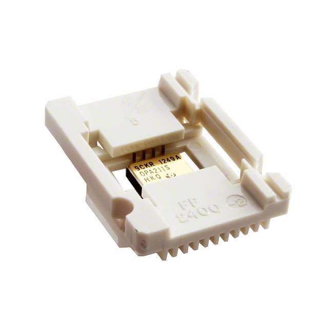
| 产品图片 |
|
| rohs | 符合RoHS无铅 / 符合限制有害物质指令(RoHS)规范要求 |
| 产品系列 | 放大器 IC,运算放大器 - 运放,Texas Instruments LMV844MT/NOPB- |
| 数据手册 | |
| 产品型号 | LMV844MT/NOPB |
| 产品目录页面 | |
| 产品种类 | 运算放大器 - 运放 |
| 供应商器件封装 | 14-TSSOP |
| 共模抑制比—最小值 | 77 dB |
| 关闭 | No Shutdown |
| 其它名称 | LMV844MT |
| 包装 | 管件 |
| 压摆率 | 2.5 V/µs |
| 商标 | Texas Instruments |
| 增益带宽生成 | 4.5 MHz |
| 增益带宽积 | 4.5MHz |
| 安装类型 | 表面贴装 |
| 安装风格 | SMD/SMT |
| 封装 | Tube |
| 封装/外壳 | 14-TSSOP(0.173",4.40mm 宽) |
| 封装/箱体 | TSSOP-14 |
| 工作温度 | -40°C ~ 125°C |
| 工作电源电压 | 2.7 V to 12 V |
| 工厂包装数量 | 94 |
| 放大器类型 | 通用 |
| 最大工作温度 | + 125 C |
| 最小工作温度 | - 40 C |
| 标准包装 | 94 |
| 电压-电源,单/双 (±) | 2.7 V ~ 12 V, ±1.35 V ~ 6 V |
| 电压-输入失调 | 50µV |
| 电流-电源 | 1.03mA |
| 电流-输入偏置 | 0.3pA |
| 电流-输出/通道 | 37mA |
| 电源电流 | 0.93 mA |
| 电路数 | 4 |
| 系列 | LMV844 |
| 设计资源 | http://www.digikey.com/product-highlights/cn/zh/texas-instruments-webench-design-center/3176 |
| 转换速度 | 2.5 V/us |
| 输入偏压电流—最大 | 10 pA |
| 输入补偿电压 | 0.5 mV |
| 输出电流 | 32 mA |
| 输出类型 | 满摆幅 |
| 通道数量 | 4 Channel |


- 商务部:美国ITC正式对集成电路等产品启动337调查
- 曝三星4nm工艺存在良率问题 高通将骁龙8 Gen1或转产台积电
- 太阳诱电将投资9.5亿元在常州建新厂生产MLCC 预计2023年完工
- 英特尔发布欧洲新工厂建设计划 深化IDM 2.0 战略
- 台积电先进制程称霸业界 有大客户加持明年业绩稳了
- 达到5530亿美元!SIA预计今年全球半导体销售额将创下新高
- 英特尔拟将自动驾驶子公司Mobileye上市 估值或超500亿美元
- 三星加码芯片和SET,合并消费电子和移动部门,撤换高东真等 CEO
- 三星电子宣布重大人事变动 还合并消费电子和移动部门
- 海关总署:前11个月进口集成电路产品价值2.52万亿元 增长14.8%


PDF Datasheet 数据手册内容提取
Product Order Technical Tools & Support & Folder Now Documents Software Community LMV841,LMV842,LMV844 SNOSAT1I–OCTOBER2006–REVISEDOCTOBER2017 LMV84x CMOS Input, RRIO, Low Power, Wide Supply Range, 4.5-MHz Operational Amplifiers 1 Features 3 Description • UnlessOtherwiseNoted,TypicalValuesat The LMV84x devices are low-voltage and low-power 1 operational amplifiers that operate with supply T =25°C,V+=5V. A voltages ranging from 2.7 V to 12 V and have rail-to- • Small5-PinSC70Package(2.00mm×1.25mm rail input and output capability. Their low offset ×0.95mm) voltage, low supply current, and CMOS inputs make • WideSupplyVoltageRange:2.7Vto12V them ideal for high impedance sensor interface and battery-poweredapplications. • SpecifiedPerformanceat3.3V,5Vand ±5V • LowSupplyCurrent:1mAPerChannel The single LMV841 is offered in the space-saving 5- pin SC70 package, the dual LMV842 in the 8-pin • UnityGainBandwidth:4.5MHz VSSOP and 8-pin SOIC packages, and the quad • Open-LoopGain:133dB LMV844 in the 14-pin TSSOP and 14-pin SOIC • InputOffsetVoltage:500µVMaximum packages. These small packages are ideal solutions forarea-constrainedPCBsandportableelectronics. • InputBiasCurrent:0.3pA • CMRRat112dBandPSSRat108dB DeviceInformation(1) • InputVoltageNoise:20nV/√Hz PARTNUMBER PACKAGE BODYSIZE(NOM) • TemperatureRange:−40°Cto125°C LMV841 SC70(5) 2.00mm×1.25mm • Rail-to-RailInputandOutput(RRIO) VSSOP(8) 3.00mm×3.00mm LMV842 SOIC(8) 4.90mm×3.91mm 2 Applications SOIC(14) 8.65mm×3.91mm LMV844 • HighImpedanceSensorInterface TSSOP(14) 5.00mm×4.40mm • Battery-PoweredInstrumentation (1) For all available packages, see the orderable addendum at • HighGainandInstrumentationAmplifiers theendofthedatasheet. • DACBuffersandActiveFilters TypicalApplications VIN - - + + Active Band-Pass Filter SENSOR RS - + RS + VS +- - LOAD High Impedance Sensor Interface High-Side, Current-Sensing CMOS Input Feature Rail-to-Rail Input and Output Feature Copyright © 2016,Texas Instruments Incorporated 1 An IMPORTANT NOTICE at the end of this data sheet addresses availability, warranty, changes, use in safety-critical applications, intellectualpropertymattersandotherimportantdisclaimers.PRODUCTIONDATA.
LMV841,LMV842,LMV844 SNOSAT1I–OCTOBER2006–REVISEDOCTOBER2017 www.ti.com Table of Contents 1 Features.................................................................. 1 7.4 DeviceFunctionalModes........................................17 2 Applications........................................................... 1 7.5 InterfacingtoHighImpedanceSensor ..................20 3 Description............................................................. 1 8 ApplicationandImplementation........................ 21 4 RevisionHistory..................................................... 2 8.1 ApplicationInformation............................................21 8.2 TypicalApplications................................................21 5 PinConfigurationandFunctions......................... 3 9 PowerSupplyRecommendations...................... 25 6 Specifications......................................................... 4 10 Layout................................................................... 25 6.1 AbsoluteMaximumRatings......................................4 6.2 ESDRatings..............................................................4 10.1 LayoutGuidelines.................................................25 6.3 RecommendedOperatingConditions.......................4 10.2 LayoutExample....................................................25 6.4 ThermalInformation..................................................4 11 DeviceandDocumentationSupport................. 26 6.5 ElectricalCharacteristics–3.3V .............................5 11.1 RelatedLinks........................................................26 6.6 ElectricalCharacteristics–5V ................................6 11.2 ReceivingNotificationofDocumentationUpdates26 6.7 ElectricalCharacteristics–±5-V ..............................7 11.3 CommunityResources..........................................26 6.8 TypicalCharacteristics............................................10 11.4 Trademarks...........................................................26 7 DetailedDescription............................................ 16 11.5 ElectrostaticDischargeCaution............................26 7.1 Overview.................................................................16 11.6 Glossary................................................................26 7.2 FunctionalBlockDiagram.......................................16 12 Mechanical,Packaging,andOrderable Information........................................................... 26 7.3 FeatureDescription.................................................16 4 Revision History NOTE:Pagenumbersforpreviousrevisionsmaydifferfrompagenumbersinthecurrentversion. ChangesfromRevisionH(July2016)toRevisionI Page • ChangedESDRatingstablefootnotestoTIstandard .......................................................................................................... 4 • ChangedThermalInformationtable....................................................................................................................................... 4 • ChangedPhaseMarginvsC graphic ................................................................................................................................ 13 L • ChangedOvershootvsC graphic....................................................................................................................................... 14 L ChangesfromRevisionG(February2013)toRevisionH Page • AddedESDRatingstable,FeatureDescriptionsection,DeviceFunctionalModes,ApplicationandImplementation section,PowerSupplyRecommendationssection,Layoutsection,DeviceandDocumentationSupportsection,and Mechanical,Packaging,andOrderableInformationsection.................................................................................................. 1 ChangesfromRevisionF(February2013)toRevisionG Page • ChangedlayoutofNationalSemiconductorDataSheettoTIformat.................................................................................. 23 2 SubmitDocumentationFeedback Copyright©2006–2017,TexasInstrumentsIncorporated ProductFolderLinks:LMV841 LMV842 LMV844
LMV841,LMV842,LMV844 www.ti.com SNOSAT1I–OCTOBER2006–REVISEDOCTOBER2017 5 Pin Configuration and Functions DCKPackage 5-PinSC70 DorDGKPackage TopView 8-PinSOICandVSSOP TopView DorPWPackage 14-PinSOICandTSSOP TopView PinFunctions PIN DESCRIPTION NAME I/O. +IN I NoninvertingInput –IN I InvertingInput OUT O Output V+ P PositiveSupply V– P NegativeSupply Copyright©2006–2017,TexasInstrumentsIncorporated SubmitDocumentationFeedback 3 ProductFolderLinks:LMV841 LMV842 LMV844
LMV841,LMV842,LMV844 SNOSAT1I–OCTOBER2006–REVISEDOCTOBER2017 www.ti.com 6 Specifications 6.1 Absolute Maximum Ratings See (1)(2) MIN MAX UNIT V differential –300 300 mV IN Supplyvoltage(V+–V−) 13.2 V Voltageatinputandoutputpins V++0.3 V−–0.3 V Inputcurrent 10 mA Junctiontemperature (3) 150 °C Soldering Infraredorconvection(20s) 235 °C information Wavesolderingleadtemperature(10s) 260 °C Storagetemperature,T −65 150 °C stg (1) StressesbeyondthoselistedunderAbsoluteMaximumRatingsmaycausepermanentdamagetothedevice.Thesearestressratings onlyandfunctionaloperationofthedeviceattheseconditionsisnotimplied.Exposuretoabsolute-maximum-ratedconditionsfor extendedperiodsmayaffectdevicereliability. (2) IfMilitary/Aerospacespecifieddevicesarerequired,contacttheTexasInstrumentsSalesOffice/Distributorsforavailabilityand specifications. (3) ThemaximumpowerdissipationisafunctionofT ,R ,andT .Themaximumallowablepowerdissipationatanyambient J(MAX) θJA A temperatureisP =(T -T )/R .AllnumbersapplyforpackagessoldereddirectlyontoaPCB. D J(MAX) A θJA 6.2 ESD Ratings VALUE UNIT Electrostatic Human-bodymodel(HBM)(1) ±2000 V V (ESD) discharge Charged-devicemodel(CDM),perJEDECspecificationJESD22-C101(2) ±250 (1) JEDECdocumentJEP155statesthat500-VHBMallowssafemanufacturingwithastandardESDcontrolprocess. (2) JEDECdocumentJEP157statesthat250-VCDMallowssafemanufacturingwithastandardESDcontrolprocess. 6.3 Recommended Operating Conditions MIN MAX UNIT Temperature(1) −40 125 °C Supplyvoltage(V+–V−) 2.7 12 V (1) ThemaximumpowerdissipationisafunctionofT ,R ,andT .Themaximumallowablepowerdissipationatanyambient J(MAX) θJA A temperatureisP =(T –T )/R .AllnumbersapplyforpackagessoldereddirectlyontoaPCB. D J(MAX) A θJA 6.4 Thermal Information LMV84x THERMALMETRIC(1) DCK(SC70) DGK D(SOIC) PW UNIT (VSSOP) (TSSOP) 5PINS 8PINS 8PINS 14PIN 14PINS R Junction-to-ambientthermalresistance(2) 269.9 179.2 121.4 85.4 113.3 °C/W θJA R Junction-to-case(top)thermalresistance 93.8 69.2 65.7 43.5 38.9 °C/W θJC(top) R Junction-to-boardthermalresistance 48.8 99.7 62.0 39.8 56.3 °C/W θJB ψ Junction-to-topcharacterizationparameter 2.0 10.0 16.5 9.2 3.1 °C/W JT ψ Junction-to-boardcharacterizationparameter 47.9 98.3 61.4 39.6 55.6 °C/W JB R Junction-to-case(bottom)thermalresistance N/A N/A N/A N/A N/A °C/W θJC(bot) (1) Formoreinformationabouttraditionalandnewthermalmetrics,seetheSemiconductorandICPackageThermalMetricsapplication report. (2) ThemaximumpowerdissipationisafunctionofT ,R ,andT .Themaximumallowablepowerdissipationatanyambient J(MAX) θJA A temperatureisP =(T -T )/R .AllnumbersapplyforpackagessoldereddirectlyontoaPCB. D J(MAX) A θJA 4 SubmitDocumentationFeedback Copyright©2006–2017,TexasInstrumentsIncorporated ProductFolderLinks:LMV841 LMV842 LMV844
LMV841,LMV842,LMV844 www.ti.com SNOSAT1I–OCTOBER2006–REVISEDOCTOBER2017 6.5 Electrical Characteristics – 3.3 V Unlessotherwisespecified,alllimitsareensuredforT =25°C,V+=3.3V,V−=0V,V =V+/2,andR >10MΩtoV+/ A CM L 2.(1) PARAMETER TESTCONDITIONS MIN(2) TYP(3) MAX(2) UNIT –500 ±50 500 V Inputoffsetvoltage µV OS atthetemperatureextremes –800 800 Inputoffsetvoltagedrift (4) 0.5 TCV µV/°C OS atthetemperatureextremes –5 5 Inputbiascurrent (4) (5) 0.3 10 I pA B atthetemperatureextremes 300 I Inputoffsetcurrent 40 fA OS Common-moderejectionratio 84 112 LMV841 0V≤VCM≤3.3V atthetemperature dB 80 extremes CMRR Common-moderejectionratio 77 106 LMV842andLMV844 0V≤VCM≤3.3V atthetemperature dB 75 extremes 86 108 2.7V≤V+≤12V,V =V+ PSRR Powersupplyrejectionratio /2 O atthetemperature 82 dB extremes Inputcommon-modevoltage CMRR≥50dB,atthetemperatureextremes CMVR –0.1 3.4 V range 100 123 R =2kΩ VOL =0.3Vto3V atthetemperature 96 dB extremes A Largesignalvoltagegain VOL 100 131 R =10kΩ VOL =0.2Vto3.1V atthetemperature 96 dB extremes 52 80 RL=2kΩtoV+/2 atthetemperature mV 120 Outputswinghigh, extremes (measuredfromV+) 28 50 RL=10kΩtoV+/2 atthetemperature mV 70 extremes V O 65 100 RL=2kΩtoV+/2 atthetemperature mV 120 Outputswinglow, extremes (measuredfromV−) 33 65 RL=10kΩtoV+/2 atthetemperature mV 75 extremes (1) Electricaltablevaluesapplyonlyforfactorytestingconditionsatthetemperatureindicated.Factorytestingconditionsresultinvery limitedself-heatingofthedevice. (2) Limitsare100%productiontestedat25°C.Limitsovertheoperatingtemperaturerangeareensuredthroughcorrelationsusing statisticalqualitycontrol(SQC)method. (3) Typicalvaluesrepresentthemostlikelyparametricnormasdeterminedatthetimeofcharacterization.Actualtypicalvaluesmayvary overtimeandwillalsodependontheapplicationandconfiguration.Thetypicalvaluesarenottestedandarenotensuredonshipped productionmaterial. (4) Thisparameterisensuredbydesignand/orcharacterizationandisnottestedinproduction. (5) Positivecurrentcorrespondstocurrentflowingintothedevice. Copyright©2006–2017,TexasInstrumentsIncorporated SubmitDocumentationFeedback 5 ProductFolderLinks:LMV841 LMV842 LMV844
LMV841,LMV842,LMV844 SNOSAT1I–OCTOBER2006–REVISEDOCTOBER2017 www.ti.com Electrical Characteristics – 3.3 V (continued) Unlessotherwisespecified,alllimitsareensuredforT =25°C,V+=3.3V,V−=0V,V =V+/2,andR >10MΩtoV+/ A CM L 2.(1) PARAMETER TESTCONDITIONS MIN(2) TYP(3) MAX(2) UNIT 20 32 SourcingV =V+/2 VIN=100mOV atthetemperature 15 mA extremes I Outputshort-circuitcurrent(6)(7) O 20 27 SinkingV =V+/2 VIN=−10O0mV atthetemperature 15 mA extremes 0.93 1.5 IS Supplycurrent Perchannel atthetemperature mA 2 extremes SR Slewrate (8) AV=1,VO=2.3VPP 2.5 V/µs 10%to90% GBW Gainbandwidthproduct 4.5 MHz Φ Phasemargin 67 Deg m en Input-referredvoltagenoise f=1kHz 20 nV/ R Open-loopoutputimpedance f=3MHz 70 Ω OUT f=1kHz,A =1 THD+N Totalharmonicdistortion+noise V 0.005% R =10kΩ L C Inputcapacitance 7 pF IN (6) ThemaximumpowerdissipationisafunctionofT ,R ,andT .Themaximumallowablepowerdissipationatanyambient J(MAX) θJA A temperatureisP =(T –T )/R .AllnumbersapplyforpackagessoldereddirectlyontoaPCB. D J(MAX) A θJA (7) Shortcircuittestisamomentarytest. (8) Numberspecifiedistheslowerofpositiveandnegativeslewrates. 6.6 Electrical Characteristics – 5 V Unlessotherwisespecified,alllimitsareensuredforT =25°C,V+=5V,V−=0V,V =V+/2,andR >10MΩtoV+/2.(1) A CM L PARAMETER TESTCONDITIONS MIN(2) TYP(3) MAX(2) UNIT –500 ±50 500 V Inputoffsetvoltage µV OS atthetemperatureextremes –800 800 TCV 0.35 OS Inputoffsetvoltagedrift(4) µV/°C atthetemperatureextremes –5 5 0.3 10 I Inputbiascurrent(4)(5) pA B atthetemperatureextremes 300 I Inputoffsetcurrent 40 fA OS 86 112 Common-moderejectionratio LMV841 0V≤VCM≤5V atthetemperature 80 dB extremes CMRR 81 106 Common-moderejectionratio LMV842andLMV844 0V≤VCM≤5V atthetemperature 79 dB extremes 86 108 2.7V≤V+≤12V,V = PSRR Powersupplyrejectionratio V+/2 O atthetemperature 82 dB extremes (1) Electricaltablevaluesapplyonlyforfactorytestingconditionsatthetemperatureindicated.Factorytestingconditionsresultinvery limitedself-heatingofthedevice. (2) Limitsare100%productiontestedat25°C.Limitsovertheoperatingtemperaturerangeareensuredthroughcorrelationsusing statisticalqualitycontrol(SQC)method. (3) Typicalvaluesrepresentthemostlikelyparametricnormasdeterminedatthetimeofcharacterization.Actualtypicalvaluesmayvary overtimeandwillalsodependontheapplicationandconfiguration.Thetypicalvaluesarenottestedandarenotensuredonshipped productionmaterial. (4) Thisparameterisensuredbydesignand/orcharacterizationandisnottestedinproduction. (5) Positivecurrentcorrespondstocurrentflowingintothedevice. 6 SubmitDocumentationFeedback Copyright©2006–2017,TexasInstrumentsIncorporated ProductFolderLinks:LMV841 LMV842 LMV844
LMV841,LMV842,LMV844 www.ti.com SNOSAT1I–OCTOBER2006–REVISEDOCTOBER2017 Electrical Characteristics – 5 V (continued) Unlessotherwisespecified,alllimitsareensuredforT =25°C,V+=5V,V−=0V,V =V+/2,andR >10MΩtoV+/2.(1) A CM L PARAMETER TESTCONDITIONS MIN(2) TYP(3) MAX(2) UNIT CMVR Inputcommon-modevoltage CMRR≥50dB,atthetemperatureextremes –0.2 5.2 V range 100 125 R =2kΩ VOL =0.3Vto4.7V atthetemperature 96 dB extremes A Largesignalvoltagegain VOL 100 133 R =10kΩ VOL =0.2Vto4.8V atthetemperature 96 dB extremes 68 100 RL=2kΩtoV+/2 atthetemperature mV 120 Outputswinghigh, extremes (measuredfromV+) 32 50 RL=10kΩtoV+/2 atthetemperature mV 70 extremes V O 78 120 RL=2kΩtoV+/2 atthetemperature mV 140 Outputswinglow, extremes (measuredfromV–) 38 70 RL=10kΩtoV+/2 atthetemperature mV 80 extremes 20 33 SourcingV =V+/2 VIN=100mOV atthetemperature 15 mA extremes I Outputshort-circuitcurrent(6) (7) O 20 28 SinkingV =V+/2 VIN=−10O0mV atthetemperature 15 mA extremes 0.96 1.5 IS Supplycurrent Perchannel atthetemperature mA 2 extremes SR Slewrate (8) AV=1,VO=4VPP 2.5 V/µs 10%to90% GBW Gainbandwidthproduct 4.5 MHz Φ Phasemargin 67 Deg m en Input-referredvoltagenoise f=1kHz 20 nV/ R Open-loopoutputimpedance f=3MHz 70 Ω OUT Totalharmonicdistortion+ f=1kHz,A =1 THD+N V 0.003% noise R =10kΩ L C Inputcapacitance 6 pF IN (6) ThemaximumpowerdissipationisafunctionofT ,R ,andT .Themaximumallowablepowerdissipationatanyambient J(MAX) θJA A temperatureisP =(T -T )/R .AllnumbersapplyforpackagessoldereddirectlyontoaPCB. D J(MAX) A θJA (7) Shortcircuittestisamomentarytest. (8) Numberspecifiedistheslowerofpositiveandnegativeslewrates. 6.7 Electrical Characteristics – ±5-V Unlessotherwisespecified,alllimitsareensuredforT =25°C,V+=5V,V−=–5V,V =0V,andR >10MΩtoV .(1) A CM L CM (1) Electricaltablevaluesapplyonlyforfactorytestingconditionsatthetemperatureindicated.Factorytestingconditionsresultinvery limitedself-heatingofthedevice. Copyright©2006–2017,TexasInstrumentsIncorporated SubmitDocumentationFeedback 7 ProductFolderLinks:LMV841 LMV842 LMV844
LMV841,LMV842,LMV844 SNOSAT1I–OCTOBER2006–REVISEDOCTOBER2017 www.ti.com Electrical Characteristics – ±5-V (continued) Unlessotherwisespecified,alllimitsareensuredforT =25°C,V+=5V,V−=–5V,V =0V,andR >10MΩtoV .(1) A CM L CM PARAMETER TESTCONDITIONS MIN(2) TYP(3) MAX(2) UNIT –500 ±50 500 V Inputoffsetvoltage µV OS atthetemperatureextremes –800 800 TCV Inputoffsetvoltagedrift (4) 0.25 OS µV/°C atthetemperatureextremes –5 5 Inputbiascurrent (4) (5) 0.3 10 I pA B atthetemperatureextremes 300 I Inputoffsetcurrent 40 fA OS 86 112 Common-moderejectionratio LMV841 –5V≤VCM≤5V atthetemperature 80 dB extremes CMRR 86 106 Common-moderejectionratio LMV842andLMV844 –5V≤VCM≤5V atthetemperature 80 dB extremes 86 108 2.7V≤V+≤12V,V = PSRR Powersupplyrejectionratio 0V O atthetemperature 82 dB extremes CMVR Inputcommon-modevoltage CMRR≥50dB –5.2 5.2 V range R =2kΩ 100 126 L VO=−4.7Vto4.7V atthetemperature dB 96 extremes A Largesignalvoltagegain VOL R =10kΩ 100 136 L VO=−4.8Vto4.8V atthetemperature dB 96 extremes 95 130 RL=2kΩto0V atthetemperature mV 155 Outputswinghigh, extremes (measuredfromV+) 44 75 RL=10kΩto0V atthetemperature mV 95 extremes V O 105 160 RL=2kΩto0V atthetemperature mV 200 Outputswinglow, extremes (measuredfromV−) 52 80 RL=10kΩto0V atthetemperature mV 100 extremes 20 37 SourcingV =0V VIN=100mOV atthetemperature 15 mA extremes I Outputshort-circuitcurrent (6) (7) O 20 29 SinkingV =0V VIN=−10O0mV atthetemperature 15 mA extremes (2) Limitsare100%productiontestedat25°C.Limitsovertheoperatingtemperaturerangeareensuredthroughcorrelationsusing statisticalqualitycontrol(SQC)method. (3) Typicalvaluesrepresentthemostlikelyparametricnormasdeterminedatthetimeofcharacterization.Actualtypicalvaluesmayvary overtimeandwillalsodependontheapplicationandconfiguration.Thetypicalvaluesarenottestedandarenotensuredonshipped productionmaterial. (4) Thisparameterisensuredbydesignand/orcharacterizationandisnottestedinproduction. (5) Positivecurrentcorrespondstocurrentflowingintothedevice. (6) ThemaximumpowerdissipationisafunctionofT ,R ,andT .Themaximumallowablepowerdissipationatanyambient J(MAX) θJA A temperatureisP =(T -T )/R .AllnumbersapplyforpackagessoldereddirectlyontoaPCB. D J(MAX) A θJA (7) Shortcircuittestisamomentarytest. 8 SubmitDocumentationFeedback Copyright©2006–2017,TexasInstrumentsIncorporated ProductFolderLinks:LMV841 LMV842 LMV844
LMV841,LMV842,LMV844 www.ti.com SNOSAT1I–OCTOBER2006–REVISEDOCTOBER2017 Electrical Characteristics – ±5-V (continued) Unlessotherwisespecified,alllimitsareensuredforT =25°C,V+=5V,V−=–5V,V =0V,andR >10MΩtoV .(1) A CM L CM PARAMETER TESTCONDITIONS MIN(2) TYP(3) MAX(2) UNIT 1.03 1.7 IS Supplycurrent Perchannel atthetemperature mA 2 extremes SR Slewrate (8) AV=1,VO=9VPP 2.5 V/µs 10%to90% GBW Gainbandwidthproduct 4.5 MHz Φ Phasemargin 67 Deg m en Input-referredvoltagenoise f=1kHz 20 nV/ R Open-loopoutputimpedance f=3MHz 70 Ω OUT f=1kHz,A =1 THD+N Totalharmonicdistortion+noise V 0.006% R =10kΩ L C Inputcapacitance 3 pF IN (8) Numberspecifiedistheslowerofpositiveandnegativeslewrates. Copyright©2006–2017,TexasInstrumentsIncorporated SubmitDocumentationFeedback 9 ProductFolderLinks:LMV841 LMV842 LMV844
LMV841,LMV842,LMV844 SNOSAT1I–OCTOBER2006–REVISEDOCTOBER2017 www.ti.com 6.8 Typical Characteristics AtT =25°C,R =10kΩ,V =5V.Unlessotherwisespecified. A L S 200 200 VS = 3.3V VS = 5.0V 150 150 125°C 100 100 85°C 50 50 V) V) 125°C P P (S 0 (S 0 O O 85°C V V -50 -50 -100 -100 25°C 25°C -150 -150 -40°C -40°C -200 -200 -1 0 1 2 3 4 -1 0 1 2 3 4 5 6 VCM (V) VCM (V) Figure1.V vsV OverTemperatureat3.3V Figure2.V vsV OverTemperatureat5V OS CM OS CM 200 200 VS = ±5V 150 150 125°C 100 100 50 85°C 50 125°C V) V) P P (OS 0 25°C (OS 0 85°C V V -50 -50 -100 -40°C -100 25°C -150 -150 -40°C -200 -200 -6 -4 -2 0 2 4 6 2 4 6 8 10 12 14 VCM (V) VSUPPLY (V) Figure3.VOSvsVCMOverTemperatureat±5V Figure4.VOSvsSupplyVoltage 200 140 RL = 10 k: 150 100 B) 130 RL = 2 k: d V) 50 GAIN ( 120 (PS 0 3.3V OP O O V -50 N L 110 RL = 600(cid:214) E ±5V P -100 5V O 100 -150 -200 90 -50 -25 0 25 50 75 100 125 0 100 200 300 400 500 TEMPERATURE (°C) OUTPUT SWING FROM RAIL (mV) Figure5.VOSvsTemperature Figure6.DCGainvsVOUT 10 SubmitDocumentationFeedback Copyright©2006–2017,TexasInstrumentsIncorporated ProductFolderLinks:LMV841 LMV842 LMV844
LMV841,LMV842,LMV844 www.ti.com SNOSAT1I–OCTOBER2006–REVISEDOCTOBER2017 Typical Characteristics (continued) AtT =25°C,R =10kΩ,V =5V.Unlessotherwisespecified. A L S 0.20 20 TA = 25°C TA = 85°C 0.15 15 0.10 10 0.05 5 A) A) p p (S 0 (S 0 A A IBI -0.05 IBI -5 5.0V 5V -0.10 -10 ±5V ±5V -0.15 3.3V -15 3.3V -0.20 -20 -5 -4 -3 -2 -1 0 1 2 3 4 5 -5 -4 -3 -2 -1 0 1 2 3 4 5 VCM (V) VCM (V) Figure7.InputBiasCurrentvsV Figure8.InputBiasCurrentvsV CM CM 200 1.4 TA = 125°C 125°C 150 1.3 100 A) m 50 NT ( 1.2 A) E p R 85°C I (BIAS -500 5.0V Y CUR 1.1 PL 1.0 25°C P -100 U ±5V S 0.9 -150 3.3V -40°C -200 0.8 -5 -4 -3 -2 -1 0 1 2 3 4 5 2 4 6 8 10 12 14 VCM (V) SUPPLY VOLTAGE (V) Figure9.InputBiasCurrentvsVCM Figure10.SupplyCurrentPerChannelvsSupplyVoltage 40 45 125°C 85°C 35 -40°C 25°C 40 A) A) m I (mSINK 30 (SOURCE 35 25°C I -40°C 25 30 85°C 125°C 20 25 2 4 6 8 10 12 2 4 6 8 10 12 SUPPLY VOLTAGE (V) SUPPLY VOLTAGE (V) Figure11.SinkingCurrentvsSupplyVoltage Figure12.SourcingCurrentvsSupplyVoltage Copyright©2006–2017,TexasInstrumentsIncorporated SubmitDocumentationFeedback 11 ProductFolderLinks:LMV841 LMV842 LMV844
LMV841,LMV842,LMV844 SNOSAT1I–OCTOBER2006–REVISEDOCTOBER2017 www.ti.com Typical Characteristics (continued) AtT =25°C,R =10kΩ,V =5V.Unlessotherwisespecified. A L S 135 65 RL = 2 k: RL = 10 k: 125 60 125°C V) 115 V) 55 125°C m m H ( 105 85°C H ( 50 G G 85°C HI 95 HI 45 L L AI 85 AI 40 R R M M RO 75 25°C RO 35 25°C F 65 F 30 UT UT -40°C O 55 -40°C O 25 V V 45 20 35 15 2 4 6 8 10 12 14 2 4 6 8 10 12 14 SUPPLY VOLTAGE (V) SUPPLY VOLTAGE (V) Figure13.OutputSwingHighvsSupplyVoltageRL=2kΩ Figure14.OutputSwingHighvsSupplyVoltageRL=10kΩ 150 75 RL = 2 k: RL = 10 k: 140 70 125°C 125°C V) 130 V) 65 m m W ( 120 85°C W ( 60 85°C O O L 110 L 55 L L RAI 100 RAI 50 M M O 90 O 45 R R 25°C FT 80 25°C FT 40 OU 70 OU 35 -40°C V V -40°C 60 30 50 25 2 4 6 8 10 12 14 2 4 6 8 10 12 14 SUPPLY VOLTAGE (V) SUPPLY VOLTAGE (V) Figure15.OutputSwingLowvsSupplyVoltageR =2kΩ Figure16.OutputSwingLowvsSupplyVoltageR =10kΩ L L 0.5 60 130 SINK 85°C GAIN 0.4 125°C PHASE 0.3 -40°C V) -40°C 40 90 L( 0.2 25°C ROM RAI 0.01 VS= 3.3V, 5.0V, +/-5V AIN (dB) 20 125°C-40°C 50 PHASE (°) F -0.1 25°C G T -40°C U O -0.2 0 10 V -0.3 125°C 85°C 125°C -0.4 CL = 20 pF SOURCE -20 -30 -0.5 10k 100k 1M 10M 0 5 10 15 20 25 30 FREQUENCY (Hz) ILOAD(mA) Figure18.Open-LoopFrequencyResponseOver Figure17.OutputVoltageSwingvsLoadCurrent Temperature 12 SubmitDocumentationFeedback Copyright©2006–2017,TexasInstrumentsIncorporated ProductFolderLinks:LMV841 LMV842 LMV844
LMV841,LMV842,LMV844 www.ti.com SNOSAT1I–OCTOBER2006–REVISEDOCTOBER2017 Typical Characteristics (continued) AtT =25°C,R =10kΩ,V =5V.Unlessotherwisespecified. A L S 60 130 80 GAIN Vs = 3.3 V PHASE 70 Vs = 5 V Vs = 10 V V =10V S 40 CL=20 pF 90 60 50 AIN (dB) 20 CVLS = = 130.30V pF 50 PHASE (°) qPHASE () 3400 G 20 0 10 10 VS = 3.3V, 5.0V, 10V 0 -20 CL = 20 pF, 50 pF, 100 pF -30 1 2 3 4567 10 20 30 5070100 200 500 1000 10k 100k 1M 10M CLOAD D001 Figure20.PhaseMarginvsC L FREQUENCY (Hz) Figure19.Open-LoopFrequencyResponseOverLoad Conditions 120 3.3V 110 5.0V 3.3V 100 ±5V 5.0V 80 90 )Bd( R 60 3.3V +PSRR RR (dB) ±5V RSP 5.0V±5V CM 70 40 3.3V: VCM = 1V 50 3.3V : VCM = 1V 20 5.0V: VCM = 2.5V -PSRR 5.0V : VC M = 2.5V ±5V: VCM = 0V ±5V : VCM = 0V 0 30 100 1k 10k 100k 1M 100 1k 10k 100k 1M FREQUENCY (Hz) FREQUENCY (Hz) Figure21.PSRRvsFrequency Figure22.CMRRvsFrequency 180 B) 160 d N ( O 140 TI V RA DI PA 120 mV/ L SE 500 E 100 N N f = 250 kHz CHA 80 AV = + 1 VIN = 2 VPP VS = 3.3V, 5.0V, ±5V CL = 20 pF 60 100 1k 10k 100k 1M 400 ns/DIV FREQUENCY (Hz) Figure23.ChannelSeparationvsFrequency Figure24.LargeSignalStepResponseWithGain=1 Copyright©2006–2017,TexasInstrumentsIncorporated SubmitDocumentationFeedback 13 ProductFolderLinks:LMV841 LMV842 LMV844
LMV841,LMV842,LMV844 SNOSAT1I–OCTOBER2006–REVISEDOCTOBER2017 www.ti.com Typical Characteristics (continued) AtT =25°C,R =10kΩ,V =5V.Unlessotherwisespecified. A L S DIV DIV mV/ mV/ 200 50 f = 250 kHz f = 250 kHz AV = +10 AV = +1 VIN = 100 mVPP VIN = 200 mVPP CL = 20 pF CL = 20 pF 400 ns/DIV 400 ns/DIV Figure25.LargeSignalStepResponseWithGain=10 Figure26.SmallSignalStepResponseWithGain=1 3.0 2.5 FALLING EDGE s) µ V V/ DI E ( mV/ AT 2.0 20 W R RISING EDGE E f = 250 kHz SL AV= +1 AV = +10 1.5 VIN= 2 VPP VIN = 10 mVPP RL= 10 kΩ CL = 20 pF CL= 20 pF 400 ns/DIV 1.0 2 4 6 8 10 12 SUPPLYVOLTAGE (V) Figure27.SmallSignalStepResponseWithGain=10 Figure28.SlewRatevsSupplyVoltage 35 100 30 25 %) 50 OT ( 20 Hz) O V/ 3.3V H n RS 15 E ( E S OV 10 NOI 5.0V 20 V(s) = 3.3 V 5 V(s) = 5 V V(s) = ±5 V 0 10 ±5V 10 20 30 4050 70 100 200 300 5007001000 CLOAD (pF) D002 10 100 1k 10k 100k Figure29.OvershootvsC FREQUENCY(Hz) L Figure30.InputVoltageNoisevsFrequency 14 SubmitDocumentationFeedback Copyright©2006–2017,TexasInstrumentsIncorporated ProductFolderLinks:LMV841 LMV842 LMV844
LMV841,LMV842,LMV844 www.ti.com SNOSAT1I–OCTOBER2006–REVISEDOCTOBER2017 Typical Characteristics (continued) AtT =25°C,R =10kΩ,V =5V.Unlessotherwisespecified. A L S 1 10 VS= 5V RL= 10 kΩ CL= 50 pF AV= +10 1 VOUT= 4.5 VPP 0.1 %) AV= +10 %) (N N ( D + D + 0.1 H H T 0.01 T 0.01 VS= 5V AV= +1 RL= 10 kΩ CL= 20 pF AV= +1 f = 1 kHz 0.001 0.001 10 100 1k 10k 100k 0.001 0.01 0.1 1 10 FREQUENCY(Hz) VOUT(V) Figure31.THD+NvsFrequency Figure32.THD+NvsV OUT 100 10 100x :) 1 (T U O 10x R 0.1 1x 0.01 0.001 100 1k 10k 100k 1M 10M FREQUENCY (Hz) Figure33.Closed-LoopOutputImpedancevsFrequency Copyright©2006–2017,TexasInstrumentsIncorporated SubmitDocumentationFeedback 15 ProductFolderLinks:LMV841 LMV842 LMV844
LMV841,LMV842,LMV844 SNOSAT1I–OCTOBER2006–REVISEDOCTOBER2017 www.ti.com 7 Detailed Description 7.1 Overview The LMV84x devices are operational amplifiers with near-precision specifications: low noise, low temperature drift, low offset, and rail-to-rail input and output. Possible application areas include instrumentation, medical, test equipment,audio,andautomotiveapplications. Its low supply current of 1 mA per amplifier, temperature range of −40°C to +125°C, 12-V supply with CMOS input, and the small SC70 package for the LMV841 make the LMV84x a unique op amp family and a perfect choiceforportableelectronics. 7.2 Functional Block Diagram 7.3 Feature Description 7.3.1 InputProtection The LMV84x devices have a set of anti-parallel diodes D and D between the input pins, as shown in Figure 34. 1 2 These diodes are present to protect the input stage of the amplifier. At the same time, they limit the amount of differentialinputvoltagethatisallowedontheinputpins. A differential signal larger than one diode voltage drop can damage the diodes. The differential signal between theinputsneedstobelimitedto ±300mVortheinputcurrentneedstobelimitedto ±10mA. NOTE When the op amp is slewing, a differential input voltage exists that forward-biases the protection diodes. This may result in current being drawn from the signal source. While this current is already limited by the internal resistors R and R (both 130 Ω), a resistor of 1 2 1 kΩ can be placed in the feedback path, or a 500-Ω resistor can be placed in series with theinputsignalforfurtherlimitation. 16 SubmitDocumentationFeedback Copyright©2006–2017,TexasInstrumentsIncorporated ProductFolderLinks:LMV841 LMV842 LMV844
LMV841,LMV842,LMV844 www.ti.com SNOSAT1I–OCTOBER2006–REVISEDOCTOBER2017 Feature Description (continued) + V + V ESD ESD - IN+ V R1 D1D2 + VOUT IN- - + V R2 ESD ESD - V - V Figure34. ProtectionDiodesBetweentheInputPins 7.3.2 InputStage The input stage of this amplifier consists of both a PMOS and an NMOS input pair to achieve a rail-to-rail input range. For input voltages close to the negative rail, only the PMOS pair is active. Close to the positive rail, only the NMOS pair is active. In a transition region that extends from approximately 2 V below V+ to 1 V below V+, both pairs are active, and one pair gradually takes over from the other. In this transition region, the input-referred offsetvoltagechangesfromtheoffsetvoltageassociatedwiththePMOSpairtothatoftheNMOSpair.Theinput pairs are trimmed independently to ensure an input offset voltage of less then 0.5 mV at room temperature over the complete rail-to-rail input range. This also significantly improves the CMRR of the amplifier in the transition region. NOTE The CMRR and PSRR limits in the tables are large-signal numbers that express the maximum variation of the input offset of the amplifier over the full common-mode voltage and supply voltage range, respectively. When the common-mode input voltage of the amplifier is within the transition region, the small signal CMRR and PSRR may be slightly lowerthanthelargesignallimits. 7.4 Device Functional Modes 7.4.1 DrivingCapacitiveLoad The LMV84x can be connected as noninverting unity gain amplifiers. This configuration is the most sensitive to capacitive loading. The combination of a capacitive load placed on the output of an amplifier along with the output impedance of the amplifier creates a phase lag, which reduces the phase margin of the amplifier. If the phase margin is significantly reduced, the response is under-damped, which causes peaking in the transfer. Whenthereistoomuchpeaking,theopampmightstartoscillating. The LMV84x can directly drive capacitive loads up to 100 pF without any stability issues. To drive heavier capacitive loads, an isolation resistor (R ) must be used, as shown in Figure 35. By using this isolation resistor, ISO the capacitive load is isolated from the output of the amplifier, and hence, the pole caused by C is no longer in L the feedback loop. The larger the value of R , the more stable the output voltage is. If values of R are ISO ISO sufficiently large, the feedback loop is stable, independent of the value of C . However, larger values of R L ISO resultinreducedoutputswingandreducedoutputcurrentdrive. Copyright©2006–2017,TexasInstrumentsIncorporated SubmitDocumentationFeedback 17 ProductFolderLinks:LMV841 LMV842 LMV844
LMV841,LMV842,LMV844 SNOSAT1I–OCTOBER2006–REVISEDOCTOBER2017 www.ti.com Device Functional Modes (continued) - RISO VOUT + VIN CL Figure35. IsolatingCapacitiveLoad 7.4.2 NoisePerformance TheLMV84xdeviceshavegoodnoisespecificationsandarefrequentlyusedinlow-noiseapplications.Therefore it is important to determine the noise of the total circuit. Besides the input-referred noise of the op amp, the feedbackresistorsmayhaveanimportantcontributiontothetotalnoise. For applications with a voltage input configuration, in general it is beneficial general, beneficial to keep the resistor values low. In these configurations high resistor values mean high noise levels. However, using low resistor values will increase the power consumption of the application. This is not always acceptable for portable applications,sothereisatrade-offbetweennoiselevelandpowerconsumption. Besides the noise contribution of the signal source, three types of noise need to be taken into account for calculatingthenoiseperformanceofanopampcircuit: • Input-referredvoltagenoiseoftheopamp • Input-referredcurrentnoiseoftheopamp • Noisesourcesoftheresistorsinthefeedbacknetwork,configuringtheopamp To calculate the noise voltage at the output of the op amp, the first step is to determine a total equivalent noise source.Thisrequiresthetransformationofallnoisesourcestothesamereferencenode.Aconvenientchoicefor this node is the input of the op amp circuit. The next step is to add all the noise sources. The final step is to multiplythetotalequivalentinputvoltagenoisewiththegainoftheopampconfiguration. If the input-referred voltage noise of the op amp is already placed at the input, the user can use the input- referred voltage noise without further transferring. The input-referred current noise needs to be converted to an input-referred voltage noise. The current noise is negligibly small, as long as the equivalent resistance is not unrealistically large, so the user can leave the current noise out for these examples. That leaves the user with the noise sources of the resistors, being the thermal noise voltage. The influence of the resistors on the total noisecanbeseeninthefollowingexamples,onewithhighresistorvaluesandonewithlowresistorvalues.Both examples describe an op amp configuration with a gain of 101 which gives the circuit a bandwidth of 44.5 kHz. The op amp noise is the same for both cases, that is, an input-referred noise voltage of 20 nV/ and a negligiblysmallinput-referrednoisecurrent. + en in - RF RG Figure36. NoiseCircuit 18 SubmitDocumentationFeedback Copyright©2006–2017,TexasInstrumentsIncorporated ProductFolderLinks:LMV841 LMV842 LMV844
LMV841,LMV842,LMV844 www.ti.com SNOSAT1I–OCTOBER2006–REVISEDOCTOBER2017 Device Functional Modes (continued) To calculate the noise of the resistors in the feedback network, the equivalent input-referred noise resistance is needed.FortheexampleinFigure36,thisequivalentresistanceR canbecalculatedusingEquation1: eq R ´R R = F G eq R +R F G (1) ThevoltagenoiseoftheequivalentresistancecanbecalculatedusingEquation2: e = 4kTR nr eq where • e =thermalnoisevoltageoftheequivalentresistor nr • R (V/ ) eq • k=Boltzmannconstant(1.38x10⁻²³J/K) • T=absolutetemperature(K) • R =resistance(Ω) (2) eq ThetotalequivalentinputvoltagenoiseisgivenbyEquation3: e = e 2 +e 2 nin nv nr where • e =totalinputequivalentvoltagenoiseofthecircuit nin • e =inputvoltagenoiseoftheopamp (3) nv The final step is multiplying the total input voltage noise by the noise gain using Equation 4, which is in this case thegainoftheopampconfiguration: e =e ´ A nout nin noise (4) The equivalent resistance for the first example with a resistor R of 10 MΩ and a resistor R of 100 kΩ at 25°C F G (298K)equalsEquation5: R ´R 10 MW´100kW R = F G = =99 kW eq R +R 10 MW+100kW F G (5) NowthenoiseoftheresistorscanbecalculatedusingEquation6,yielding: e = 4kTR nr eq = 4´1.38´10-23J/K´298K´99 kW =40 nV/ Hz (6) ThetotalnoiseattheinputoftheopampiscalculatedinEquation7: e = e 2 +e 2 nin nv nr = (20 nV/ Hz)2 +(40 nV/ Hz)2 = 45nV/ Hz (7) Forthefirstexample,thisinputnoise,multipliedwiththenoisegain,inEquation8 givesatotaloutputnoiseof: e =e ´A nout nin noise =45 nV/ Hz´101=4.5 mV/ Hz (8) In the second example, with a resistor R of 10 kΩ and a resistor R of 100 Ω at 25°C (298 K), the equivalent F G resistanceequalsEquation9: R ´R 10 kW´100 W R = F G = =99 W eq R +R 10 kW+100 W F G (9) TheresistornoiseforthesecondexampleiscalculatedinEquation10: Copyright©2006–2017,TexasInstrumentsIncorporated SubmitDocumentationFeedback 19 ProductFolderLinks:LMV841 LMV842 LMV844
LMV841,LMV842,LMV844 SNOSAT1I–OCTOBER2006–REVISEDOCTOBER2017 www.ti.com Device Functional Modes (continued) e = 4kTR nr eq = 4´1.38´10-23J/K´298K´99 W =1nV/ Hz (10) ThetotalnoiseattheinputoftheopampiscalculatedinEquation10: e = e 2 +e 2 nin nv nr = (20 nV/ Hz)2 +(1nV/ Hz)2 =20 nV/ Hz (11) Forthesecondexampletheinputnoise,multipliedwiththenoisegain,inEquation12givesanoutputnoiseof: e =e ´A nout nin noise =20 nV/ Hz´101=2 mV/ Hz (12) In the first example the noise is dominated by the resistor noise due to the very high resistor values, in the second example the very low resistor values add only a negligible contribution to the noise and now the dominating factor is the op amp itself. When selecting the resistor values, it is important to choose values that do not add extra noise to the application. Choosing values above 100 kΩ may increase the noise too much. Low values keep the noise within acceptable levels; choosing very low values however, does not make the noise evenlower,butcanincreasethecurrentofthecircuit. 7.5 Interfacing to High Impedance Sensor WithCMOSinputs,theLMV84xareparticularlysuitedtobeusedashighimpedancesensorinterfaces. Many sensors have high source impedances that may range up to 10 MΩ. The input bias current of an amplifier loads the output of the sensor, and thus cause a voltage drop across the source resistance, as shown in Figure37.Whenanopampisselectedwitharelativelyhighinputbiascurrent,thiserrormaybeunacceptable. The low input current of the LMV84x significantly reduces such errors. The following examples show the differencebetweenastandardopampinputandtheCMOSinputoftheLMV84x. ThevoltageattheinputoftheopampcanbecalculatedwithEquation13: V =V –I ×R (13) IN+ S B S For a standard op amp, the input bias Ib can be 10 nA. When the sensor generates a signal of 1 V (V ) and the S sensorsimpedanceis10MΩ (R ),thesignalattheopampinputiscalculatedinEquation14: S V =1V–10nA×10MΩ=1V-0.1V=0.9V (14) IN FortheCMOSinputoftheLMV84x,whichhasaninputbiascurrentofonly0.3pA,thiswouldgiveEquation15: V =1V–0.3pA×10MΩ=1V–3µV=0.999997V (15) IN The conclusion is that a standard op amp, with its high input bias current input, is not a good choice for use in impedance sensor applications. The LMV84x devices, in contrast, are much more suitable due to the low input bias current. The error is negligibly small; therefore, the LMV84x are a must for use with high-impedance sensors. SENSOR + V RS IB VIN+ + VS + - - - V Figure37. HighImpedanceSensorInterface 20 SubmitDocumentationFeedback Copyright©2006–2017,TexasInstrumentsIncorporated ProductFolderLinks:LMV841 LMV842 LMV844
LMV841,LMV842,LMV844 www.ti.com SNOSAT1I–OCTOBER2006–REVISEDOCTOBER2017 8 Application and Implementation NOTE Information in the following applications sections is not part of the TI component specification, and TI does not warrant its accuracy or completeness. TI’s customers are responsible for determining suitability of components for their purposes. Customers should validateandtesttheirdesignimplementationtoconfirmsystemfunctionality. 8.1 Application Information The rail-to-rail input and output of the LMV84x and the wide supply voltage range make these amplifiers ideal to use in numerous applications. Three sample applications, namely the active filter circuit, high-side current sensing,andthermocouplesensorinterface,areprovidedintheTypicalApplicationssection. 8.2 Typical Applications 8.2.1 ActiveFilterCircuit C C R2 R2 R1 C - R1 C - R3 + R3 + Figure38. ActiveBand-PassFilterImplementation 8.2.1.1 DesignRequirements In this example it is required to design a bandpass filter with band-pass frequency of 10 kHz, and a center frequence of approximately 10% from the total frequence of the filter. This is achieved by cascading two band- passfilters,AandB,withslightlydifferentcenterfrequencies. 8.2.1.2 DetailedDesignProcedure Thecenterfrequencyoftheseparateband-passfiltersA,andBcanbecalculatedbyEquation16: 1 R +R f = 1 3 mid 2pC RR R 1 2 3 where • C=33nF • R1=2KΩ • R2=6.2KΩ • andR3=45Ω (16) ThisgivesEquation17forfilterA: 1 2 kW+6.2 kW f = =9.2 kHz mid p´33 nF 2 kW´6.2 kW´45 kW (17) andEquation18forfilterBwithC=27nF: 1 2 kW+6.2 kW f = =11.2 kHz mid p´27 nF 2 kW´6.2 kW´45 kW (18) BandwidthcanbecalculatedbyEquation19: Copyright©2006–2017,TexasInstrumentsIncorporated SubmitDocumentationFeedback 21 ProductFolderLinks:LMV841 LMV842 LMV844
LMV841,LMV842,LMV844 SNOSAT1I–OCTOBER2006–REVISEDOCTOBER2017 www.ti.com Typical Applications (continued) 1 B = pR C 2 (19) ForfilterA,thisgivesEquation20: 1 B = =1.6 kHz p´6.2 kW´33 nF (20) andEquation21forfilterB: 1 B = =1.9 kHz p´6.2 kW´27 nF (21) 8.2.1.3 ApplicationCurve The responses of filter A and filter B are shown as the thin lines in Figure 39; the response of the combined filter is shown as the thick line. Shifting the center frequencies of the separate filters farther apart, results in a wider band; however, positioning the center frequencies too far apart results in a less flat gain within the band. For widerbandsmoreband-passfilterscanbecascaded. 10 FILTER A FILTER B 0 B) -10 d N ( AI G -20 -30 COMBINED FILTER -40 1k 10k 100k FREQUENCY (Hz) Figure39. ActiveBand-PassFilterCurve NOTE UsetheWEBENCHinternettoolsatwww.ti.com foryourfilterapplication. 8.2.2 High-Side,Current-SensingCircuit V+ RF RG - RS + RG RF LOAD Z Figure40. High-Side,Current-SensingCircuit 22 SubmitDocumentationFeedback Copyright©2006–2017,TexasInstrumentsIncorporated ProductFolderLinks:LMV841 LMV842 LMV844
LMV841,LMV842,LMV844 www.ti.com SNOSAT1I–OCTOBER2006–REVISEDOCTOBER2017 Typical Applications (continued) 8.2.2.1 DesignRequirements In this example, it is desired to measure a current between 0 A and 2 A using a sense resistor of 100 mΩ, and convertittoanoutputvoltageof0to5V.Acurrentof2Aflowingthroughtheloadandthesenseresistorresults inavoltageof200mVacrossthesenseresistor.Theopampamplifiesthis200mVtofitthecurrentrangetothe outputvoltagerange. 8.2.2.2 DetailedDesignProcedure To measure current at a point in a circuit, a sense resistor is placed in series with the load, as shown in Figure 40. The current flowing through this sense resistor results in a voltage drop, that is amplified by the op amp. The rail-to-rail input and the low V features make the LMV84x ideal op amps for high-side, current- OS sensingapplications. TheinputandtheoutputrelationofthecircuitisgivenbyEquation22: V =R /R ×V (22) OUT F G SENSE Foraloadcurrentof2Aandanoutputvoltageof5VthegainwouldbeV /V =25. OUT SENSE If the feedback resistor, R , is 100 kΩ, then the value for R is 4 kΩ. The tolerance of the resistors has to be low F G toobtainagoodcommon-moderejection. 8.2.3 ThermocoupleSensorSignalAmplification Figure41isatypicalexampleforathermocoupleamplifierapplicationusinganLMV841,LMV842,orLMV844.A thermocouple senses a temperature and converts it into a voltage. This signal is then amplified by the LMV841, LMV842, or LMV844. An ADC can then convert the amplified signal to a digital signal. For further processing the digital signal can be processed by a microprocessor, and can be used to display or log the temperature, or the temperaturedatacanbeusedinafabricationprocess. Cold junction Temperature LM35 RG RF T Metal A - Copper RG LMV8 41 + Amplified Metal B Copper Thermocouple Thermocouple Output RF Cold junction Reference Figure41. ThermocoupleSensorInterface 8.2.3.1 DesignRequirements Inthisexampleitisdesiredtomeasuretemperatureintherangeof0°Cto500°Cwitharesolutionof0.5°Cusing aK-typethermocouplesensor.ThepowersupplyforboththeLMV84xandtheADCis 3.3V. 8.2.3.2 DetailedDesignProcedure A thermocouple is a junction of two different metals. These metals produce a small voltage that increases with temperature. A K-type thermocouple is a very common temperature sensor made of a junction between nickel- chromium and nickel-aluminum. There are several reasons for using the K-type thermocouple. These include temperaturerange,thelinearity,thesensitivity,andthecost. Copyright©2006–2017,TexasInstrumentsIncorporated SubmitDocumentationFeedback 23 ProductFolderLinks:LMV841 LMV842 LMV844
LMV841,LMV842,LMV844 SNOSAT1I–OCTOBER2006–REVISEDOCTOBER2017 www.ti.com Typical Applications (continued) A K-type thermocouple has a wide temperature range. The range of this thermocouple is from approximately −200°C to approximately 1200°C, as can be seen in Figure 42. This covers the generally used temperature ranges. Over the main part of the range the behavior is linear. This is important for converting the analog signal to a digital signal. The K-type thermocouple has good sensitivity when compared to many other types; the sensitivity is 41 µV/°C. Lower sensitivity requires more gain and makes the application more sensitive to noise. In addition, a K-type thermocouple is not expensive, many other thermocouples consist of more expensive materials or are moredifficulttoproduce. 50 V) m 40 E( G TA 30 L O V E 20 L P U O C 10 O M R HE 0 T -10 -200 0 200 400 600 800 1000 1200 TEMPERATURE (°C) Figure42. K-TypeThermocoupleResponse The temperature range of 0°C to 500°C results in a voltage range from 0 mV to 20.6 mV produced by the thermocouple.ThisisshowninFigure42. To obtain the best accuracy the full ADC range of 0 to 3.3 V is used and the gain needed for this full range can becalculatedEquation23: A =3.3V/0.0206V=160 (23) V If R is 2 kΩ, then the value for R can be calculated with this gain of 160. Because A = R / R , R can be G F V F G F calculatedinEquation24: R =A ×R =160×2kΩ=320kΩ (24) F V G To achieve a resolution of 0.5°C a step smaller than the minimum resolution is needed. This means that at least 1000 steps are necessary (500°C/0.5°C). A 10-bit ADC would be sufficient as this gives 1024 steps. A 10-bit ADCsuchasthetwochannel10-bitADC102S021wouldbeagoodchoice. At the point where the thermocouple wires are connected to the circuit on the PCB unwanted parasitic thermocoupleisformed,introducingerrorinthemeasurementsoftheactualthermocouplesensor. Using an isothermal block as a reference will compensate for this additional thermocouple effect. An isothermal block is a good heat conductor. This means that the two thermocouple connections both have the same temperature. The temperature of the isothermal block can be measured, and thereby the temperature of the thermocouple connections. This is usually called the cold junction reference temperature. In the example, an LM35 is used to measure this temperature. This semiconductor temperature sensor can accurately measure temperaturesfrom −55°Cto150°C. TheADCinthisexamplealsocovertsthesignalfromtheLM35toadigitalsignal,hence,themicroprocessorcan compensatefortheamplifiedthermocouplesignaloftheunwantedthermocouplejunctionattheconnector. 24 SubmitDocumentationFeedback Copyright©2006–2017,TexasInstrumentsIncorporated ProductFolderLinks:LMV841 LMV842 LMV844
LMV841,LMV842,LMV844 www.ti.com SNOSAT1I–OCTOBER2006–REVISEDOCTOBER2017 9 Power Supply Recommendations The LMV84x is specified for operation from 2.7 V to 12 V (±1.35 V to ±6 V) over a –40°C to 125°C temperature range. Parameters that can exhibit significant variance with regard to operating voltage or temperature are presentedintheAbsoluteMaximumRatings. CAUTION Supplyvoltageslargerthan13.2Vcanpermanentlydamagethedevice. For proper operation, the power supplies must be properly decoupled. For decoupling the supply lines, TI suggests placing 10-nF capacitors as close as possible to the operational amplifier power supply pins. For single supply, place a capacitor between V+ and V– supply leads. For dual supplies, place one capacitor between V+ andground,andonecapacitorbetweenV–andground. 10 Layout 10.1 Layout Guidelines • TheV+pinmustbebypassedtogroundwithalow-ESRcapacitor. • TheoptimumplacementisclosesttotheV+andgroundpins. • TakecaretominimizetheloopareaformedbythebypasscapacitorconnectionbetweenV+andground. • ThegroundpinmustbeconnectedtothePCBgroundplaneatthepinofthedevice. • Thefeedbackcomponentsmustbeplacedasclosetothedeviceaspossibletominimizestrays. 10.2 Layout Example Place components close to device and to each other to reduce parasitic error VOUTA Place low-ESR ceramic bypass capacitor close to device Run the input traces as far away from the supply lines as possible RF OUTA V+ GND RG GND -INA OUTB VIN +INA -INB V- +INB Place low-ESR ceramic bypass capacitor close to GND device VS- Figure43. LayoutExample(TopView) Copyright©2006–2017,TexasInstrumentsIncorporated SubmitDocumentationFeedback 25 ProductFolderLinks:LMV841 LMV842 LMV844
LMV841,LMV842,LMV844 SNOSAT1I–OCTOBER2006–REVISEDOCTOBER2017 www.ti.com 11 Device and Documentation Support 11.1 Related Links The table below lists quick access links. Categories include technical documents, support and community resources,toolsandsoftware,andquickaccesstoordernow. Table1.RelatedLinks TECHNICAL TOOLS& SUPPORT& PARTS PRODUCTFOLDER ORDERNOW DOCUMENTS SOFTWARE COMMUNITY LMV841 Clickhere Clickhere Clickhere Clickhere Clickhere LMV842 Clickhere Clickhere Clickhere Clickhere Clickhere LMV844 Clickhere Clickhere Clickhere Clickhere Clickhere 11.2 Receiving Notification of Documentation Updates To receive notification of documentation updates, navigate to the device product folder on ti.com. In the upper right corner, click on Alert me to register and receive a weekly digest of any product information that has changed.Forchangedetails,reviewtherevisionhistoryincludedinanyreviseddocument. 11.3 Community Resources The following links connect to TI community resources. Linked contents are provided "AS IS" by the respective contributors. They do not constitute TI specifications and do not necessarily reflect TI's views; see TI's Terms of Use. TIE2E™OnlineCommunity TI'sEngineer-to-Engineer(E2E)Community.Createdtofostercollaboration amongengineers.Ate2e.ti.com,youcanaskquestions,shareknowledge,exploreideasandhelp solveproblemswithfellowengineers. DesignSupport TI'sDesignSupport QuicklyfindhelpfulE2Eforumsalongwithdesignsupporttoolsand contactinformationfortechnicalsupport. 11.4 Trademarks E2EisatrademarkofTexasInstruments. Allothertrademarksarethepropertyoftheirrespectiveowners. 11.5 Electrostatic Discharge Caution Thesedeviceshavelimitedbuilt-inESDprotection.Theleadsshouldbeshortedtogetherorthedeviceplacedinconductivefoam duringstorageorhandlingtopreventelectrostaticdamagetotheMOSgates. 11.6 Glossary SLYZ022—TIGlossary. Thisglossarylistsandexplainsterms,acronyms,anddefinitions. 12 Mechanical, Packaging, and Orderable Information The following pages include mechanical, packaging, and orderable information. This information is the most current data available for the designated devices. This data is subject to change without notice and revision of thisdocument.Forbrowser-basedversionsofthisdatasheet,refertotheleft-handnavigation. 26 SubmitDocumentationFeedback Copyright©2006–2017,TexasInstrumentsIncorporated ProductFolderLinks:LMV841 LMV842 LMV844
PACKAGE OPTION ADDENDUM www.ti.com 13-May-2019 PACKAGING INFORMATION Orderable Device Status Package Type Package Pins Package Eco Plan Lead/Ball Finish MSL Peak Temp Op Temp (°C) Device Marking Samples (1) Drawing Qty (2) (6) (3) (4/5) LMV841MG/NOPB ACTIVE SC70 DCK 5 1000 Green (RoHS CU SN Level-1-260C-UNLIM -40 to 125 A97 & no Sb/Br) LMV841MGX/NOPB ACTIVE SC70 DCK 5 3000 Green (RoHS CU SN Level-1-260C-UNLIM -40 to 125 A97 & no Sb/Br) LMV842MA/NOPB ACTIVE SOIC D 8 95 Green (RoHS CU SN Level-1-260C-UNLIM -40 to 125 LMV84 & no Sb/Br) 2MA LMV842MAX/NOPB ACTIVE SOIC D 8 2500 Green (RoHS CU SN Level-1-260C-UNLIM -40 to 125 LMV84 & no Sb/Br) 2MA LMV842MM/NOPB ACTIVE VSSOP DGK 8 1000 Green (RoHS CU NIPDAUAG | CU SN Level-1-260C-UNLIM -40 to 125 AC4A & no Sb/Br) LMV842MMX/NOPB ACTIVE VSSOP DGK 8 3500 Green (RoHS CU NIPDAUAG | CU SN Level-1-260C-UNLIM -40 to 125 AC4A & no Sb/Br) LMV844MA/NOPB ACTIVE SOIC D 14 55 Green (RoHS CU SN | Call TI Level-1-260C-UNLIM -40 to 125 LMV844MA & no Sb/Br) LMV844MAX/NOPB ACTIVE SOIC D 14 2500 Green (RoHS CU SN | Call TI Level-1-260C-UNLIM -40 to 125 LMV844MA & no Sb/Br) LMV844MT/NOPB ACTIVE TSSOP PW 14 94 Green (RoHS CU SN Level-1-260C-UNLIM -40 to 125 LMV844 & no Sb/Br) MT LMV844MTX/NOPB ACTIVE TSSOP PW 14 2500 Green (RoHS CU SN Level-1-260C-UNLIM -40 to 125 LMV844 & no Sb/Br) MT (1) The marketing status values are defined as follows: ACTIVE: Product device recommended for new designs. LIFEBUY: TI has announced that the device will be discontinued, and a lifetime-buy period is in effect. NRND: Not recommended for new designs. Device is in production to support existing customers, but TI does not recommend using this part in a new design. PREVIEW: Device has been announced but is not in production. Samples may or may not be available. OBSOLETE: TI has discontinued the production of the device. (2) RoHS: TI defines "RoHS" to mean semiconductor products that are compliant with the current EU RoHS requirements for all 10 RoHS substances, including the requirement that RoHS substance do not exceed 0.1% by weight in homogeneous materials. Where designed to be soldered at high temperatures, "RoHS" products are suitable for use in specified lead-free processes. TI may reference these types of products as "Pb-Free". RoHS Exempt: TI defines "RoHS Exempt" to mean products that contain lead but are compliant with EU RoHS pursuant to a specific EU RoHS exemption. Green: TI defines "Green" to mean the content of Chlorine (Cl) and Bromine (Br) based flame retardants meet JS709B low halogen requirements of <=1000ppm threshold. Antimony trioxide based flame retardants must also meet the <=1000ppm threshold requirement. (3) MSL, Peak Temp. - The Moisture Sensitivity Level rating according to the JEDEC industry standard classifications, and peak solder temperature. Addendum-Page 1
PACKAGE OPTION ADDENDUM www.ti.com 13-May-2019 (4) There may be additional marking, which relates to the logo, the lot trace code information, or the environmental category on the device. (5) Multiple Device Markings will be inside parentheses. Only one Device Marking contained in parentheses and separated by a "~" will appear on a device. If a line is indented then it is a continuation of the previous line and the two combined represent the entire Device Marking for that device. (6) Lead/Ball Finish - Orderable Devices may have multiple material finish options. Finish options are separated by a vertical ruled line. Lead/Ball Finish values may wrap to two lines if the finish value exceeds the maximum column width. Important Information and Disclaimer:The information provided on this page represents TI's knowledge and belief as of the date that it is provided. TI bases its knowledge and belief on information provided by third parties, and makes no representation or warranty as to the accuracy of such information. Efforts are underway to better integrate information from third parties. TI has taken and continues to take reasonable steps to provide representative and accurate information but may not have conducted destructive testing or chemical analysis on incoming materials and chemicals. TI and TI suppliers consider certain information to be proprietary, and thus CAS numbers and other limited information may not be available for release. In no event shall TI's liability arising out of such information exceed the total purchase price of the TI part(s) at issue in this document sold by TI to Customer on an annual basis. OTHER QUALIFIED VERSIONS OF LMV841, LMV842, LMV844 : •Automotive: LMV841-Q1, LMV842-Q1, LMV844-Q1 NOTE: Qualified Version Definitions: •Automotive - Q100 devices qualified for high-reliability automotive applications targeting zero defects Addendum-Page 2
PACKAGE MATERIALS INFORMATION www.ti.com 5-Sep-2018 TAPE AND REEL INFORMATION *Alldimensionsarenominal Device Package Package Pins SPQ Reel Reel A0 B0 K0 P1 W Pin1 Type Drawing Diameter Width (mm) (mm) (mm) (mm) (mm) Quadrant (mm) W1(mm) LMV841MG/NOPB SC70 DCK 5 1000 178.0 8.4 2.25 2.45 1.2 4.0 8.0 Q3 LMV841MGX/NOPB SC70 DCK 5 3000 178.0 8.4 2.25 2.45 1.2 4.0 8.0 Q3 LMV842MAX/NOPB SOIC D 8 2500 330.0 12.4 6.5 5.4 2.0 8.0 12.0 Q1 LMV842MM/NOPB VSSOP DGK 8 1000 178.0 12.4 5.3 3.4 1.4 8.0 12.0 Q1 LMV842MMX/NOPB VSSOP DGK 8 3500 330.0 12.4 5.3 3.4 1.4 8.0 12.0 Q1 LMV844MAX/NOPB SOIC D 14 2500 330.0 16.4 6.5 9.35 2.3 8.0 16.0 Q1 LMV844MTX/NOPB TSSOP PW 14 2500 330.0 12.4 6.95 5.6 1.6 8.0 12.0 Q1 PackMaterials-Page1
PACKAGE MATERIALS INFORMATION www.ti.com 5-Sep-2018 *Alldimensionsarenominal Device PackageType PackageDrawing Pins SPQ Length(mm) Width(mm) Height(mm) LMV841MG/NOPB SC70 DCK 5 1000 210.0 185.0 35.0 LMV841MGX/NOPB SC70 DCK 5 3000 210.0 185.0 35.0 LMV842MAX/NOPB SOIC D 8 2500 367.0 367.0 35.0 LMV842MM/NOPB VSSOP DGK 8 1000 210.0 185.0 35.0 LMV842MMX/NOPB VSSOP DGK 8 3500 367.0 367.0 35.0 LMV844MAX/NOPB SOIC D 14 2500 367.0 367.0 35.0 LMV844MTX/NOPB TSSOP PW 14 2500 367.0 367.0 35.0 PackMaterials-Page2
None
None
None
None
None
None
PACKAGE OUTLINE D0008A SOIC - 1.75 mm max height SCALE 2.800 SMALL OUTLINE INTEGRATED CIRCUIT C SEATING PLANE .228-.244 TYP [5.80-6.19] .004 [0.1] C A PIN 1 ID AREA 6X .050 [1.27] 8 1 2X .189-.197 [4.81-5.00] .150 NOTE 3 [3.81] 4X (0 -15 ) 4 5 8X .012-.020 B .150-.157 [0.31-0.51] .069 MAX [3.81-3.98] .010 [0.25] C A B [1.75] NOTE 4 .005-.010 TYP [0.13-0.25] 4X (0 -15 ) SEE DETAIL A .010 [0.25] .004-.010 0 - 8 [0.11-0.25] .016-.050 [0.41-1.27] DETAIL A (.041) TYPICAL [1.04] 4214825/C 02/2019 NOTES: 1. Linear dimensions are in inches [millimeters]. Dimensions in parenthesis are for reference only. Controlling dimensions are in inches. Dimensioning and tolerancing per ASME Y14.5M. 2. This drawing is subject to change without notice. 3. This dimension does not include mold flash, protrusions, or gate burrs. Mold flash, protrusions, or gate burrs shall not exceed .006 [0.15] per side. 4. This dimension does not include interlead flash. 5. Reference JEDEC registration MS-012, variation AA. www.ti.com
EXAMPLE BOARD LAYOUT D0008A SOIC - 1.75 mm max height SMALL OUTLINE INTEGRATED CIRCUIT 8X (.061 ) [1.55] SYMM SEE DETAILS 1 8 8X (.024) [0.6] SYMM (R.002 ) TYP [0.05] 5 4 6X (.050 ) [1.27] (.213) [5.4] LAND PATTERN EXAMPLE EXPOSED METAL SHOWN SCALE:8X SOLDER MASK SOLDER MASK METAL OPENING OPENING METAL UNDER SOLDER MASK EXPOSED METAL EXPOSED METAL .0028 MAX .0028 MIN [0.07] [0.07] ALL AROUND ALL AROUND NON SOLDER MASK SOLDER MASK DEFINED DEFINED SOLDER MASK DETAILS 4214825/C 02/2019 NOTES: (continued) 6. Publication IPC-7351 may have alternate designs. 7. Solder mask tolerances between and around signal pads can vary based on board fabrication site. www.ti.com
EXAMPLE STENCIL DESIGN D0008A SOIC - 1.75 mm max height SMALL OUTLINE INTEGRATED CIRCUIT 8X (.061 ) [1.55] SYMM 1 8 8X (.024) [0.6] SYMM (R.002 ) TYP [0.05] 5 4 6X (.050 ) [1.27] (.213) [5.4] SOLDER PASTE EXAMPLE BASED ON .005 INCH [0.125 MM] THICK STENCIL SCALE:8X 4214825/C 02/2019 NOTES: (continued) 8. Laser cutting apertures with trapezoidal walls and rounded corners may offer better paste release. IPC-7525 may have alternate design recommendations. 9. Board assembly site may have different recommendations for stencil design. www.ti.com
None
None
IMPORTANTNOTICEANDDISCLAIMER TIPROVIDESTECHNICALANDRELIABILITYDATA(INCLUDINGDATASHEETS),DESIGNRESOURCES(INCLUDINGREFERENCE DESIGNS),APPLICATIONOROTHERDESIGNADVICE,WEBTOOLS,SAFETYINFORMATION,ANDOTHERRESOURCES“ASIS” ANDWITHALLFAULTS,ANDDISCLAIMSALLWARRANTIES,EXPRESSANDIMPLIED,INCLUDINGWITHOUTLIMITATIONANY IMPLIEDWARRANTIESOFMERCHANTABILITY,FITNESSFORAPARTICULARPURPOSEORNON-INFRINGEMENTOFTHIRD PARTYINTELLECTUALPROPERTYRIGHTS. TheseresourcesareintendedforskilleddevelopersdesigningwithTIproducts.Youaresolelyresponsiblefor(1)selectingtheappropriate TIproductsforyourapplication,(2)designing,validatingandtestingyourapplication,and(3)ensuringyourapplicationmeetsapplicable standards,andanyothersafety,security,orotherrequirements.Theseresourcesaresubjecttochangewithoutnotice.TIgrantsyou permissiontousetheseresourcesonlyfordevelopmentofanapplicationthatusestheTIproductsdescribedintheresource.Other reproductionanddisplayoftheseresourcesisprohibited.NolicenseisgrantedtoanyotherTIintellectualpropertyrightortoanythird partyintellectualpropertyright.TIdisclaimsresponsibilityfor,andyouwillfullyindemnifyTIanditsrepresentativesagainst,anyclaims, damages,costs,losses,andliabilitiesarisingoutofyouruseoftheseresources. TI’sproductsareprovidedsubjecttoTI’sTermsofSale(www.ti.com/legal/termsofsale.html)orotherapplicabletermsavailableeitheron ti.comorprovidedinconjunctionwithsuchTIproducts.TI’sprovisionoftheseresourcesdoesnotexpandorotherwisealterTI’sapplicable warrantiesorwarrantydisclaimersforTIproducts. MailingAddress:TexasInstruments,PostOfficeBox655303,Dallas,Texas75265 Copyright©2019,TexasInstrumentsIncorporated