
 Datasheet下载
- 型号: LMV339M/NOPB
- 制造商: Texas Instruments
- 库位|库存: xxxx|xxxx
- 要求:
| 数量阶梯 | 香港交货 | 国内含税 |
| +xxxx | $xxxx | ¥xxxx |
查看当月历史价格
查看今年历史价格
LMV339M/NOPB产品简介:
ICGOO电子元器件商城为您提供LMV339M/NOPB由Texas Instruments设计生产,在icgoo商城现货销售,并且可以通过原厂、代理商等渠道进行代购。 LMV339M/NOPB价格参考¥3.80-¥9.44。Texas InstrumentsLMV339M/NOPB封装/规格:线性 - 比较器, 通用 比较器 CMOS,开路集电极,TTL 14-SOIC。您可以下载LMV339M/NOPB参考资料、Datasheet数据手册功能说明书,资料中有LMV339M/NOPB 详细功能的应用电路图电压和使用方法及教程。
LMV339M/NOPB 是由 Texas Instruments(德州仪器)生产的一款低功耗、单电源供电的比较器,属于 LMV33x 系列。它具有宽工作电压范围(1.6V 至 5.5V)、快速响应时间和轨到轨输入输出特性,适用于多种应用场景。以下是其主要应用场景:

 1. 过压/欠压检测
   - LMV339M 可用于监测电源电压是否超出设定范围。例如,在电池管理系统中,可以检测电池电压是否过低或过高,从而触发保护机制。
   - 应用实例:锂电池保护电路、电源监控系统。

 2. 信号电平转换
   - 该比较器可用于将模拟信号转换为数字信号,或者在不同电压电平之间进行信号转换。
   - 应用实例:传感器信号调理、逻辑电平转换。

 3. 温度监测与控制
   - 结合热敏电阻或温度传感器,LMV339M 可以检测温度变化并触发报警或控制信号。
   - 应用实例:过温保护电路、恒温控制系统。

 4. 电机驱动与保护
   - 在小型电机驱动电路中,LMV339M 可用于电流检测和过流保护,确保电机运行在安全范围内。
   - 应用实例:直流电机驱动保护、步进电机控制。

 5. 音频信号处理
   - 用于音频信号的峰值检测或电平判断,帮助实现音量控制或信号触发功能。
   - 应用实例:音频设备中的静音控制、音量指示。

 6. 通信接口保护
   - 在 UART、SPI 或 I2C 等通信接口中,LMV339M 可用于检测信号完整性或提供过压保护。
   - 应用实例:通信端口的信号完整性监控。

 7. 光耦隔离电路
   - 配合光电耦合器使用,LMV339M 能够实现信号隔离和放大,适用于工业控制和医疗设备。
   - 应用实例:隔离式信号传输、开关电源反馈控制。

 8. 智能家居与物联网设备
   - 作为核心元件之一,用于检测环境参数(如光照、湿度、气体浓度等),并将结果传递给主控芯片。
   - 应用实例:智能照明、环境监测设备。

 总结
LMV339M/NOPB 的低功耗特性和宽电压范围使其非常适合便携式设备和电池供电系统。同时,其快速响应能力也使其成为实时监测和保护应用的理想选择。无论是在消费电子、工业自动化还是汽车电子领域,这款比较器都能发挥重要作用。
| 参数 | 数值 |
| 产品目录 | 集成电路 (IC)半导体 |
| CMRR,PSRR(典型值) | - |
| 描述 | IC COMP TINY QUAD LOW V 14-SOIC模拟比较器 Low Volt Quad Comp |
| 产品分类 | |
| 品牌 | Texas Instruments |
| 产品手册 | http://www.ti.com/lit/gpn/lmv339-n |
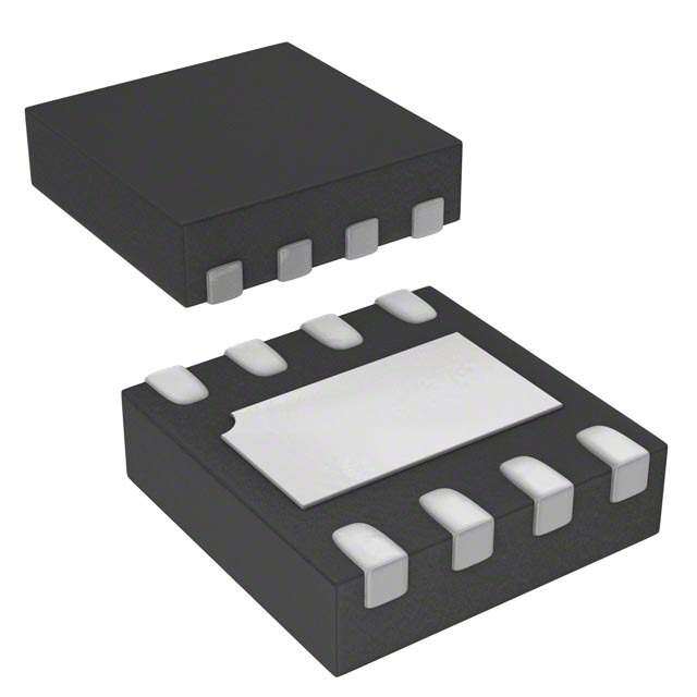
| 产品图片 |
|
| rohs | 符合RoHS无铅 / 符合限制有害物质指令(RoHS)规范要求 |
| 产品系列 | 模拟比较器,Texas Instruments LMV339M/NOPB- |
| 数据手册 | |
| 产品型号 | LMV339M/NOPB |
| PCN组件/产地 | |
| PCN设计/规格 | |
| 产品 | Analog Comparators |
| 产品目录页面 | |
| 产品种类 | 模拟比较器 |
| 传播延迟(最大值) | 600ns |
| 供应商器件封装 | 14-SOIC |
| 偏转电压—最大值 | 7 mV |
| 元件数 | 4 |
| 其它名称 | *LMV339M/NOPB |
| 制造商产品页 | http://www.ti.com/general/docs/suppproductinfo.tsp?distId=10&orderablePartNumber=LMV339M/NOPB |
| 包装 | 管件 |
| 响应时间 | 0.45 us |
| 商标 | Texas Instruments |
| 安装类型 | 表面贴装 |
| 安装风格 | SMD/SMT |
| 封装 | Tube |
| 封装/外壳 | 14-SOIC(0.154",3.90mm 宽) |
| 封装/箱体 | SOIC-14 Narrow |
| 工作温度 | -40°C ~ 85°C |
| 工厂包装数量 | 55 |
| 最大工作温度 | + 85 C |
| 最小工作温度 | - 40 C |
| 标准包装 | 55 |
| 比较器类型 | General Purpose |
| 滞后 | - |
| 电压-电源,单/双 (±) | 2.7 V ~ 5.5 V |
| 电压-输入失调(最大值) | 7mV @ 5V |
| 电压增益dB | 93.98 dB |
| 电流-输入偏置(最大值) | 0.25µA @ 5V |
| 电流-输出(典型值) | 84mA @ 5V |
| 电流-静态(最大值) | 300µA |
| 电源电压-最大 | 5 V |
| 电源电压-最小 | 2.7 V |
| 电源电流 | 300 uA |
| 电源电流—最大值 | 300 uA |
| 类型 | 通用 |
| 系列 | LMV339-N |
| 输入偏压电流—最大 | 250 nA |
| 输出类型 | Open Collector |
| 通道数量 | 4 Channel |


- 商务部:美国ITC正式对集成电路等产品启动337调查
- 曝三星4nm工艺存在良率问题 高通将骁龙8 Gen1或转产台积电
- 太阳诱电将投资9.5亿元在常州建新厂生产MLCC 预计2023年完工
- 英特尔发布欧洲新工厂建设计划 深化IDM 2.0 战略
- 台积电先进制程称霸业界 有大客户加持明年业绩稳了
- 达到5530亿美元!SIA预计今年全球半导体销售额将创下新高
- 英特尔拟将自动驾驶子公司Mobileye上市 估值或超500亿美元
- 三星加码芯片和SET,合并消费电子和移动部门,撤换高东真等 CEO
- 三星电子宣布重大人事变动 还合并消费电子和移动部门
- 海关总署:前11个月进口集成电路产品价值2.52万亿元 增长14.8%


PDF Datasheet 数据手册内容提取
Product Sample & Technical Tools & Support & Folder Buy Documents Software Community LMV331-N,LMV339-N,LMV393-N SNOS018H–AUGUST1999–REVISEDDECEMBER2014 LMV33x-N / LMV393-N General-Purpose, Low-Voltage, Tiny Pack Comparators 1 Features The LMV393-N is available in 8-pin SOIC and VSSOP packages. The LMV339-N is available in 14- • (For5-VSupply,TypicalUnlessOtherwiseNoted) 1 pinSOICandTSSOPpackages. • Ensured2.7-Vand5-VPerformance The LMV331-N/393-N/339-N is the most cost- • IndustrialTemperatureRange−40°Cto85°C effective solution where space, low voltage, low • LowSupplyCurrent60µA/Channel power, and price are the primary specification in • InputCommonModeVoltageRangeIncludes circuit design for portable consumer products. They offer specifications that meet or exceed the familiar Ground LM393/339atafractionofthesupplycurrent. • LowOutputSaturationVoltage200mV The chips are built with TI's advanced Submicron • PropagationDelay200ns Silicon-Gate BiCMOS process. The LMV331-N/393- • Space-Saving5-PinSC70and5-PinSOT23 N/339-N have bipolar input and output stages for Packages improvednoiseperformance. 2 Applications Table1.DeviceInformation(1) • MobileCommunications PARTNUMBER PACKAGE BODYSIZE(NOM) • NotebooksandPDAs SC70(5) 2.00mm×1.25mm LMV331-N • Battery-PoweredElectronics SOT-23(5) 2.90mm×1.6mm • General-PurposePortableDevices SOIC(14) 8.65mm×3.91mm LMV339-N • General-Purpose,Low-VoltageApplications TSSOP(14) 5.00mm×4.40mm SOIC(8) 4.90mm×3.91mm LMV393-N 3 Description VSSOP(8) 3.00mm×3.00mm The LMV393-N and LMV339-N are low-voltage (2.7 (1) For all available packages, see the orderable addendum at to 5 V) versions of the dual and quad comparators, theendofthedatasheet. LM393/339, which are specified at 5 to 30 V. The LMV331-N is the single version, which is available in space-saving, 5-pin SC70 and 5-pin SOT23 packages. The 5-pin SC70 is approximately half the sizeofthe5-pinSOT23. LowSupplyCurrent FastResponseTime 1 An IMPORTANT NOTICE at the end of this data sheet addresses availability, warranty, changes, use in safety-critical applications, intellectualpropertymattersandotherimportantdisclaimers.PRODUCTIONDATA.
LMV331-N,LMV339-N,LMV393-N SNOS018H–AUGUST1999–REVISEDDECEMBER2014 www.ti.com Table of Contents 1 Features.................................................................. 1 7.3 FeatureDescription...................................................9 2 Applications........................................................... 1 7.4 DeviceFunctionalModes..........................................9 3 Description............................................................. 1 8 ApplicationandImplementation........................ 10 4 RevisionHistory..................................................... 2 8.1 ApplicationInformation............................................10 8.2 TypicalApplications................................................16 5 PinConfigurationandFunctions......................... 3 9 PowerSupplyRecommendations...................... 21 6 Specifications......................................................... 4 10 Layout................................................................... 21 6.1 AbsoluteMaximumRatings .....................................4 6.2 ESDRatings..............................................................4 10.1 LayoutGuidelines.................................................21 6.3 RecommendedOperatingConditions.......................4 10.2 LayoutExample....................................................22 6.4 ThermalInformation..................................................4 11 DeviceandDocumentationSupport................. 23 6.5 2.7-VDCElectricalCharacteristics...........................4 11.1 DeviceSupport......................................................23 6.6 2.7-VACElectricalCharacteristics...........................5 11.2 DocumentationSupport........................................23 6.7 5-VDCElectricalCharacteristics..............................5 11.3 RelatedLinks........................................................23 6.8 5-VACElectricalCharacteristics..............................6 11.4 Trademarks...........................................................23 6.9 TypicalCharacteristics..............................................7 11.5 ElectrostaticDischargeCaution............................23 7 DetailedDescription.............................................. 9 11.6 Glossary................................................................23 7.1 Overview...................................................................9 12 Mechanical,Packaging,andOrderable Information........................................................... 23 7.2 FunctionalBlockDiagram.........................................9 4 Revision History NOTE:Pagenumbersforpreviousrevisionsmaydifferfrompagenumbersinthecurrentversion. ChangesfromRevisionG(Feburary2013)toRevisionH Page • AddedPinConfigurationandFunctionssection,ESDRatingstable,FeatureDescriptionsection,DeviceFunctional Modes,ApplicationandImplementationsection,PowerSupplyRecommendationssection,Layoutsection,Device andDocumentationSupportsection,andMechanical,Packaging,andOrderableInformationsection .............................. 1 2 SubmitDocumentationFeedback Copyright©1999–2014,TexasInstrumentsIncorporated ProductFolderLinks:LMV331-N LMV339-N LMV393-N
LMV331-N,LMV339-N,LMV393-N www.ti.com SNOS018H–AUGUST1999–REVISEDDECEMBER2014 5 Pin Configuration and Functions DCKandDBVPackage DandDGKPackage 5-PinSC70/SOT23 8-PinSOIC/VSSOP TopView TopView DandPWPackage 14-PinSOIC/TSSOP TopView PinFunctions PIN LMV331-N LMV393-N LMV339-N TYPE DESCRIPTION NAME DVB,DCK D,DGK PW +IN 1 - - I Noninvertinginput +INA - 3 5 I Noninvertinginput,channelA +INB - 5 7 I Noninvertinginput,channelB +INC - - 9 I Noninvertinginput,channelC +IND - - 11 I Noninvertinginput,channelD -IN 3 - - I Invertinginput -INA - 2 4 I Invertinginput,channelA -INB - 6 6 I Invertinginput,channelB -INC - - 8 I Invertinginput,channelC -IND - - 10 I Invertinginput,channelD OUT 4 - - O Output OUTA - 1 2 O Output,channelA OUTB - 7 1 O Output,channelB OUTC - - 14 O Output,channelC OUTD - - 13 O Output,channelD V+ 5 8 3 P Positive(highest)powersupply V- 2 4 12 P Negative(lowest)powersupply Copyright©1999–2014,TexasInstrumentsIncorporated SubmitDocumentationFeedback 3 ProductFolderLinks:LMV331-N LMV339-N LMV393-N
LMV331-N,LMV339-N,LMV393-N SNOS018H–AUGUST1999–REVISEDDECEMBER2014 www.ti.com 6 Specifications 6.1 Absolute Maximum Ratings overoperatingfree-airtemperaturerange(unlessotherwisenoted)(1)(2) MIN MAX UNIT DifferentialInputVoltage ±Supply Voltage Voltageonanypin(referredtoV−pin) 5.5 V SolderingInformation InfraredorConvection(20sec) 235 °C JunctionTemperature (3) 150 °C Storagetemperature,T −65 150 °C stg (1) StressesbeyondthoselistedunderAbsoluteMaximumRatingsmaycausepermanentdamagetothedevice.Thesearestressratings only,whichdonotimplyfunctionaloperationofthedeviceattheseoranyotherconditionsbeyondthoseindicatedunderRecommended OperatingConditions.Exposuretoabsolute-maximum-ratedconditionsforextendedperiodsmayaffectdevicereliability. (2) IfMilitary/Aerospacespecifieddevicesarerequired,pleasecontacttheTexasInstrumentsSalesOffice/Distributorsforavailabilityand specifications. (3) ThemaximumpowerdissipationisafunctionofT ,θ .Themaximumallowablepowerdissipationatanyambienttemperatureis J(MAX) JA P =(T -T )/θ .AllnumbersapplyforpackagessoldereddirectlyontoaPCboard. D J(MAX) A JA 6.2 ESD Ratings VALUE UNIT Human-bodymodel(HBM),perANSI/ESDA/JEDECJS-001(1) ±800 V Electrostaticdischarge V (ESD) Machinemodel ±120 (1) JEDECdocumentJEP155statesthat500-VHBMallowssafemanufacturingwithastandardESDcontrolprocess. 6.3 Recommended Operating Conditions overoperatingfree-airtemperaturerange(unlessotherwisenoted)(1) MIN MAX UNIT SupplyVoltage 2.7 5 V TemperatureRange (2) −40 85 °C (1) StressesbeyondthoselistedunderAbsoluteMaximumRatingsmaycausepermanentdamagetothedevice.Thesearestressratings only,whichdonotimplyfunctionaloperationofthedeviceattheseoranyotherconditionsbeyondthoseindicatedunderRecommended OperatingConditions.Exposuretoabsolute-maximum-ratedconditionsforextendedperiodsmayaffectdevicereliability. (2) ThemaximumpowerdissipationisafunctionofT ,θ .Themaximumallowablepowerdissipationatanyambienttemperatureis J(MAX) JA P =(T -T )/θ .AllnumbersapplyforpackagessoldereddirectlyontoaPCboard. D J(MAX) A JA 6.4 Thermal Information LMV331-N LMV339-N LMV393-N THERMALMETRIC(1) DCK DBV D PW D DGK UNIT 5PINS 5PINS 14PINS 14PINS 8PINS 8PINS R Junction-to-ambientthermalresistance 478 265 145 155 190 23 °C/W θJA (1) Formoreinformationabouttraditionalandnewthermalmetrics,seetheICPackageThermalMetricsapplicationreport,SPRA953. 6.5 2.7-V DC Electrical Characteristics Unlessotherwisespecified,alllimitsensuredforT =25°C,V+=2.7V,V−=0V. J PARAMETER TESTCONDITIONS MIN TYP MAX UNIT (1) (2) (1) V InputOffsetVoltage 1.7 7 mV OS TCV InputOffsetVoltageAverageDrift Atthetemperatureextremes 5 µV/°C OS (1) Alllimitsareensuredbytestingorstatisticalanalysis. (2) Typicalvaluesrepresentthemostlikelyparametricnormasdeterminedatthetimeofcharacterization.Actualtypicalvaluesmayvary overtimeandwillalsodependontheapplicationandconfiguration.Thetypicalvaluesarenottestedandarenotensuredonshipped productionmaterial. 4 SubmitDocumentationFeedback Copyright©1999–2014,TexasInstrumentsIncorporated ProductFolderLinks:LMV331-N LMV339-N LMV393-N
LMV331-N,LMV339-N,LMV393-N www.ti.com SNOS018H–AUGUST1999–REVISEDDECEMBER2014 2.7-V DC Electrical Characteristics (continued) Unlessotherwisespecified,alllimitsensuredforT =25°C,V+=2.7V,V−=0V. J PARAMETER TESTCONDITIONS MIN TYP MAX UNIT (1) (2) (1) I InputBiasCurrent 10 250 B nA Atthetemperatureextremes 400 I InputOffsetCurrent 5 50 OS nA Atthetemperatureextremes 150 V InputVoltageRange −0.1 V CM 2.0 V V SaturationVoltage I ≤1mA 120 mV SAT SINK I OutputSinkCurrent V ≤1.5V 5 23 mA O O I SupplyCurrent LMV331-N 40 100 µA S LMV393-N 70 140 µA BothComparators LMV339-N 140 200 µA AllfourComparators OutputLeakageCurrent .003 µA Atthetemperatureextremes 1 6.6 2.7-V AC Electrical Characteristics T =25°C,V+=2.7V,R =5.1kΩ,V−=0V. J L PARAMETER TESTCONDITIONS MIN TYP MAX UNIT (1) (2) (1) t PropagationDelay(HightoLow) InputOverdrive=10mV 1000 ns PHL InputOverdrive=100mV 350 ns t PropagationDelay(LowtoHigh) InputOverdrive=10mV 500 ns PLH InputOverdrive=100mV 400 ns (1) Alllimitsareensuredbytestingorstatisticalanalysis. (2) Typicalvaluesrepresentthemostlikelyparametricnormasdeterminedatthetimeofcharacterization.Actualtypicalvaluesmayvary overtimeandwillalsodependontheapplicationandconfiguration.Thetypicalvaluesarenottestedandarenotensuredonshipped productionmaterial. 6.7 5-V DC Electrical Characteristics Unlessotherwisespecified,alllimitsensuredforT =25°C,V+=5V,V−=0V. J PARAMETER TESTCONDITIONS MIN TYP MAX UNIT (1) (2) (1) V InputOffsetVoltage 1.7 7 OS mV Atthetemperatureextremes 9 TCV InputOffsetVoltageAverageDrift 5 µV/°C OS I InputBiasCurrent 25 250 B nA Atthetemperatureextremes 400 I InputOffsetCurrent 2 50 OS nA Atthetemperatureextremes 150 V InputVoltageRange −0.1 V CM 4.2 V A VoltageGain 20 50 V/mV V (1) Alllimitsareensuredbytestingorstatisticalanalysis. (2) Typicalvaluesrepresentthemostlikelyparametricnormasdeterminedatthetimeofcharacterization.Actualtypicalvaluesmayvary overtimeandwillalsodependontheapplicationandconfiguration.Thetypicalvaluesarenottestedandarenotensuredonshipped productionmaterial. Copyright©1999–2014,TexasInstrumentsIncorporated SubmitDocumentationFeedback 5 ProductFolderLinks:LMV331-N LMV339-N LMV393-N
LMV331-N,LMV339-N,LMV393-N SNOS018H–AUGUST1999–REVISEDDECEMBER2014 www.ti.com 5-V DC Electrical Characteristics (continued) Unlessotherwisespecified,alllimitsensuredforT =25°C,V+=5V,V−=0V. J PARAMETER TESTCONDITIONS MIN TYP MAX UNIT (1) (2) (1) V SaturationVoltage I ≤4mA 200 400 sat SINK mV Atthetemperatureextremes 700 I OutputSinkCurrent V ≤1.5V 84 10 mA O O I SupplyCurrent LMV331-N 60 120 S µA Atthetemperatureextremes 150 LMV393-N 100 200 BothComparators µA Atthetemperatureextremes 250 LMV339-N 170 300 AllfourComparators µA Atthetemperatureextremes 350 OutputLeakageCurrent .003 µA Atthetemperatureextremes 1 6.8 5-V AC Electrical Characteristics T =25°C,V+=5V,R =5.1kΩ,V−=0V. J L PARAMETER TESTCONDITIONS MIN TYP MAX UNIT (1) (2) (1) t PropagationDelay(HightoLow) InputOverdrive=10mV 600 ns PHL InputOverdrive=100mV 200 ns t PropagationDelay(LowtoHigh) InputOverdrive=10mV 450 ns PLH InputOverdrive=100mV 300 ns (1) Alllimitsareensuredbytestingorstatisticalanalysis. (2) Typicalvaluesrepresentthemostlikelyparametricnormasdeterminedatthetimeofcharacterization.Actualtypicalvaluesmayvary overtimeandwillalsodependontheapplicationandconfiguration.Thetypicalvaluesarenottestedandarenotensuredonshipped productionmaterial. 6 SubmitDocumentationFeedback Copyright©1999–2014,TexasInstrumentsIncorporated ProductFolderLinks:LMV331-N LMV339-N LMV393-N
LMV331-N,LMV339-N,LMV393-N www.ti.com SNOS018H–AUGUST1999–REVISEDDECEMBER2014 6.9 Typical Characteristics Unlessotherwisespecified,V =+5V,singlesupply,T =25°C S A Figure1.SupplyCurrentvs.SupplyVoltageOutputHigh Figure2.SupplyCurrentvs.SupplyVoltageOutputLow (LMV331-N) (LMV331-N) 500 -40°C 400 85°C )V 300 m 25°C ( T A VS 200 100 0 0 1 2 3 4 5 6 7 8 9 10 ISINK (mA) Figure3.OutputVoltagevs.OutputCurrentat5-VSupply Figure4.OutputVoltagevs.OutputCurrentat2.7-VSupply Figure5.InputBiasCurrentvs.SupplyVoltage Figure6.ResponseTimevs.InputOverdriveNegative Transition Copyright©1999–2014,TexasInstrumentsIncorporated SubmitDocumentationFeedback 7 ProductFolderLinks:LMV331-N LMV339-N LMV393-N
LMV331-N,LMV339-N,LMV393-N SNOS018H–AUGUST1999–REVISEDDECEMBER2014 www.ti.com Typical Characteristics (continued) Unlessotherwisespecified,V =+5V,singlesupply,T =25°C S A Figure7.ResponseTimeforInputOverdrivePositive Figure8.ResponseTimevs.InputOverdriveNegative Transition Transition Figure9.ResponseTimeforInputOverdrivePositiveTransition 8 SubmitDocumentationFeedback Copyright©1999–2014,TexasInstrumentsIncorporated ProductFolderLinks:LMV331-N LMV339-N LMV393-N
LMV331-N,LMV339-N,LMV393-N www.ti.com SNOS018H–AUGUST1999–REVISEDDECEMBER2014 7 Detailed Description 7.1 Overview The LMV331-N/393-N/339-N comparators features a supply voltage range of 2.7 V to 5 V with a low supply current of 55 μA/channel with propagation delays as low as 200ns. They are avaialble in small, space-saving packages, which makes these comparators versatile for use in a wide range of applications, from portable to industrial. The open collector output configuration allows the device to be used in wired-OR configurations, such asawindowcomparators. 7.2 Functional Block Diagram 7.3 Feature Description 7.3.1 OpenCollectorOutput The output of the LMV331-N/393-N/339-N series is the uncommitted collector of a grounded-emitter NPN output transistor, which requires a pull-up resistor to a positive supply voltage for the output to switch properly. Many collectors can be tied together to provide an output OR’ing function. An output pull-up resistor can be connected to any available power supply voltage within the permitted V+ supply voltage range. The output pull-up resistor should be chosen high enough so as to avoid excessive power dissipation yet low enough to supply enough drivetoswitchwhateverloadcircuitryisusedonthecomparatoroutput.OntheLMV331-N/393-N/339-Nthepull- upresistorshouldrangebetween1kto10kΩ. 7.3.2 GroundSensingInput The LMV331-N/393-N/339-N has a typical input common mode voltage range of −0.1V below the ground to 0.8V belowVcc. 7.4 Device Functional Modes Abasiccomparatorcircuitisusedforconvertinganalogsignalstoadigitaloutput. TheoutputisHIGHwhenthevoltageonthenon-inverting(+IN)inputisgreaterthantheinverting(-IN)input. TheoutputisLOWwhenthevoltageonthenon-inverting(+IN)inputislessthantheinverting(-IN)input. Theinvertinginput(-IN)isalsocommonlyreferredtoasthe"reference"or"V "input. REF Copyright©1999–2014,TexasInstrumentsIncorporated SubmitDocumentationFeedback 9 ProductFolderLinks:LMV331-N LMV339-N LMV393-N
LMV331-N,LMV339-N,LMV393-N SNOS018H–AUGUST1999–REVISEDDECEMBER2014 www.ti.com 8 Application and Implementation NOTE Information in the following applications sections is not part of the TI component specification, and TI does not warrant its accuracy or completeness. TI’s customers are responsible for determining suitability of components for their purposes. Customers should validateandtesttheirdesignimplementationtoconfirmsystemfunctionality. 8.1 Application Information 8.1.1 BasicComparator The comparator compares the input voltage (V ) at the non-inverting pin to the reference voltage (V ) at the IN REF invertingpin.IfV islessthanV ,theoutputvoltage(V )isatthesaturationvoltage.Ontheotherhand,ifV IN REF O IN isgreaterthanV ,theoutputvoltage(V )isatV . REF O CC Figure10. BasicComparator 8.1.2 ComparatorWithHysteresis The basic comparator configuration may oscillate or produce a noisy output if the applied differential input voltage is near the comparator's offset voltage. This usually happens when the input signal is moving very slowly across the switching threshold of the comparator. This problem can be prevented by the addition of hysteresis or positivefeedback. 8.1.2.1 InvertingComparatorWithHysteresis The inverting comparator with hysteresis requires a three resistor network that are referenced to the supply voltage V of the comparator. When V at the inverting input is less than V , the voltage at the non-inverting CC in a node of the comparator (V < V ), the output voltage is high (for simplicity assume V switches as high as V ). in a O CC The three network resistors can be represented as R //R in series with R . The lower input trip voltage V is 1 3 2 a1 definedas: (1) When V is greater than V (V > V ), the output voltage is low very close to ground. In this case the three in a in a networkresistorscanbepresentedasR //R inserieswithR .TheuppertripvoltageV isdefinedas: 2 3 1 a2 (2) 10 SubmitDocumentationFeedback Copyright©1999–2014,TexasInstrumentsIncorporated ProductFolderLinks:LMV331-N LMV339-N LMV393-N
LMV331-N,LMV339-N,LMV393-N www.ti.com SNOS018H–AUGUST1999–REVISEDDECEMBER2014 Application Information (continued) Thetotalhysteresisprovidedbythenetworkisdefinedas: ΔV =V -V (3) a a1 a2 To assure that the comparator will always switch fully to V and not be pulled down by the load the resistors CC valuesshouldbechosenasfollow: R <<R (4) PULL-UP LOAD andR >R . (5) 1 PULL-UP Figure11. InvertingComparatorWithHysteresis 8.1.2.1.1 Non-invertingComparatorWithHysteresis Non-inverting comparator with hysteresis requires a two resistor network, and a voltage reference (V ) at the ref inverting input. When V is low, the output is also low. For the output to switch from low to high, V must rise up in in toV whereV iscalculatedby: in1 in1 (6) WhenV ishigh,theoutputisalsohigh.Tomakethecomparatorswitchbacktoitslowstate,V mustequalV in in ref beforeV willagainequalV .V canbecalculatedby: A ref in (7) ThehysteresisofthiscircuitisthedifferencebetweenV andV . in1 in2 Copyright©1999–2014,TexasInstrumentsIncorporated SubmitDocumentationFeedback 11 ProductFolderLinks:LMV331-N LMV339-N LMV393-N
LMV331-N,LMV339-N,LMV393-N SNOS018H–AUGUST1999–REVISEDDECEMBER2014 www.ti.com Application Information (continued) ΔV =V R /R (8) in CC 1 2 Figure12. NoninvertingComparatorWithHystersis Figure13. HysteresisThresholdPoints 8.1.3 ORingtheOutput By the inherit nature of an open-collector comparator, the outputs of several comparators can be tied together with a shared pull-up resistor to V . If one or more of the comparators outputs goes low, the output V will go CC O low. 12 SubmitDocumentationFeedback Copyright©1999–2014,TexasInstrumentsIncorporated ProductFolderLinks:LMV331-N LMV339-N LMV393-N
LMV331-N,LMV339-N,LMV393-N www.ti.com SNOS018H–AUGUST1999–REVISEDDECEMBER2014 Application Information (continued) Figure14. ORingtheOutputs 8.1.4 DrivingCMOSandTTL The output of the comparator is capable of driving CMOS and TTL Logic circuits. The pull-up resistor may be pulled-up to any voltage equal to, or less than the supply voltage on V+. However, it must not be pulled-up to a voltagehigherthanV+. Figure15. DrivingCMOS Copyright©1999–2014,TexasInstrumentsIncorporated SubmitDocumentationFeedback 13 ProductFolderLinks:LMV331-N LMV339-N LMV393-N
LMV331-N,LMV339-N,LMV393-N SNOS018H–AUGUST1999–REVISEDDECEMBER2014 www.ti.com Application Information (continued) Figure16. DrivingTTL 8.1.5 ANDGates ThecomparatorcanbeusedasthreeinputANDgate.Theoperationofthegateisasfollows: The resistor divider at the inverting input establishes a reference voltage at that node. The non-inverting input is the sum of the voltages at the inputs divided by the voltage dividers. The output will go high only when all three inputsarehigh,casingthevoltageatthenon-invertinginputtogoabovethatatinvertinginput.Thecircuitvalues shownworkfora0equaltogroundanda1equalto5V. The resistor values can be altered if different logic levels are desired. If more inputs are required, diodes are recommendedtoimprovethevoltagemarginwhenallbutoneoftheinputsarehigh. Figure17. ANDGate 8.1.6 ORGates A three input OR gate is achieved from the basic AND gate simply by increasing the resistor value connected fromtheinvertinginputtoV ,therebyreducingthereferencevoltage. cc Alogic1atanyoftheinputswillproducealogic1attheoutput. 14 SubmitDocumentationFeedback Copyright©1999–2014,TexasInstrumentsIncorporated ProductFolderLinks:LMV331-N LMV339-N LMV393-N
LMV331-N,LMV339-N,LMV393-N www.ti.com SNOS018H–AUGUST1999–REVISEDDECEMBER2014 Application Information (continued) Figure18. ORGate 8.1.7 LargeFan-InGate ExtralogicinputsmaybeaddedbyORingtheinputwithmultiplediodes. Figure19. LargeFan-InandGate Copyright©1999–2014,TexasInstrumentsIncorporated SubmitDocumentationFeedback 15 ProductFolderLinks:LMV331-N LMV339-N LMV393-N
LMV331-N,LMV339-N,LMV393-N SNOS018H–AUGUST1999–REVISEDDECEMBER2014 www.ti.com 8.2 Typical Applications 8.2.1 SquarewaveOscillator Figure20. SquarewaveOscillator 8.2.1.1 DesignRequirements Comparators are ideal for oscillator applications. This square wave generator uses the minimum number of components. The output frequency is set by the RC time constant of the capacitor C and the resistor in the 1 negative feedback R . The maximum frequency is limited only by the large signal propagation delay of the 4 comparatorinadditiontoanycapacitiveloadingattheoutput,whichwoulddegradetheoutputslewrate. 8.2.1.2 DetailedDesignProcedure Figure21. SquarewaveOscillatorTimingThresholds Toanalyzethecircuit,assumethattheoutputisinitiallyhigh.Forthistobetrue,thevoltageattheinvertinginput V has to be less than the voltage at the non-inverting input V . For V to be low, the capacitor C has to be c a c 1 discharged and will charge up through the negative feedback resistor R . When it has charged up to value equal 4 tothevoltageatthepositiveinputV ,thecomparatoroutputwillswitch. a1 V willbegivenby: a1 (9) 16 SubmitDocumentationFeedback Copyright©1999–2014,TexasInstrumentsIncorporated ProductFolderLinks:LMV331-N LMV339-N LMV393-N
LMV331-N,LMV339-N,LMV393-N www.ti.com SNOS018H–AUGUST1999–REVISEDDECEMBER2014 Typical Applications (continued) If: R =R =R (10) 1 2 3 Then: V =2V /3 (11) a1 CC Whentheoutputswitchestoground,thevalueofV isreducedbythehysteresisnetworktoavaluegivenby: a V =V /3 (12) a2 CC Capacitor C must now discharge through R towards ground. The output will return to its high state when the 1 4 voltageacrossthecapacitorhasdischargedtoavalueequaltoV . a2 Forthecircuitshown,theperiodforonecycleofoscillationwillbetwicethetimeittakesforasingleRCcircuitto chargeuptoonehalfofitsfinalvalue.Thetimetochargethecapacitorcanbecalculatedfrom: (13) WhereV isthemaxappliedpotentialacrossthecapacitor=(2V /3) max CC andV =Vmax/2=V /3 C CC Oneperiodwillbegivenby: 1/freq=2t (14) orcalculatingtheexponentialgives: 1/freq=2(0.694)R C (15) 4 1 Resistors R and R must be at least two times larger than R to ensure that V will go all the way up to V in 3 4 5 O CC thehighstate.Thefrequencystabilityofthiscircuitshouldstrictlybeafunctionoftheexternalcomponents. 8.2.1.3 ApplicationCurve 5.0 4.5 V 4.0 OUT 3.5 V) 3.0 T ( 2.5 Va U O V 2.0 1.5 1.0 Vc 0.5 0.0 0 5 10 15 20 25 30 35 40 TIME (µs) C001 Figure22. WaveformsforCircuitinTypicalApplications Copyright©1999–2014,TexasInstrumentsIncorporated SubmitDocumentationFeedback 17 ProductFolderLinks:LMV331-N LMV339-N LMV393-N
LMV331-N,LMV339-N,LMV393-N SNOS018H–AUGUST1999–REVISEDDECEMBER2014 www.ti.com Typical Applications (continued) 8.2.2 CrystalControlledOscillator Figure23. CrystalControlledOscillator A simple yet very stable oscillator that generates a clock for slower digital systems can be obtained by using a resonator as the feedback element. It is similar to the squarewave oscillator, except that the positive feedback is obtained through a quartz crystal. The circuit oscillates when the transmission through the crystal is at a maximum,sothecrystalinitsseries-resonantmode. The value of R and R are equal so that the comparator will switch symmetrically about +V /2. The RC 1 2 CC constant of R and C is set to be several times greater than the period of the oscillating frequency, insuring a 3 1 50% duty cycle by maintaining a DC voltage at the inverting input equal to the absolute average of the output waveform. Whenspecifyingthecrystal,besuretoorderseriesresonantwiththedesiredtemperaturecoefficient. 18 SubmitDocumentationFeedback Copyright©1999–2014,TexasInstrumentsIncorporated ProductFolderLinks:LMV331-N LMV339-N LMV393-N
LMV331-N,LMV339-N,LMV393-N www.ti.com SNOS018H–AUGUST1999–REVISEDDECEMBER2014 Typical Applications (continued) 8.2.3 PulseGeneratorWithVariableDutyCycle Figure24. PulseGeneratorWithVariableDutyCycle The pulse generator with variable duty cycle is just a minor modification of the basic square wave generator. Providing a separate charge and discharge path for capacitor C generates a variable duty cycle. One path, 1 through R and D will charge the capacitor and set the pulse width (t ). The other path, R and D will discharge 2 2 1 1 1 thecapacitorandsetthetimebetweenpulses(t ). 2 By varying resistor R , the time between pulses of the generator can be changed without changing the pulse 1 width. Similarly, by varying R , the pulse width will be altered without affecting the time between pulses. Both 2 controlswillchangethefrequencyofthegenerator.Thepulsewidthandtimebetweenpulsescanbefoundfrom: (16) Copyright©1999–2014,TexasInstrumentsIncorporated SubmitDocumentationFeedback 19 ProductFolderLinks:LMV331-N LMV339-N LMV393-N
LMV331-N,LMV339-N,LMV393-N SNOS018H–AUGUST1999–REVISEDDECEMBER2014 www.ti.com Typical Applications (continued) Solvingtheseequationsfort andt 1 2 t =R C ln2 (17) 1 4 1 t =R C ln2 (18) 2 5 1 These terms will have a slight error due to the fact that V is not exactly equal to 2/3 V but is actually max CC reducedbythediodedropto: (19) (20) (21) 8.2.4 PositivePeakDetector Figure25. PositivePeakDetector Positive peak detector is basically the comparator operated as a unit gain follower with a large holding capacitor fromtheoutputtoground.Additionaltransistorisaddedtotheoutputtoprovidealowimpedancecurrentsource. When the output of the comparator goes high, current is passed through the transistor to charge up the capacitor. The only discharge path will be the 1-MΩ resistor shunting C1 and any load that is connected to the output. The decay time can be altered simply by changing the 1-MΩ resistor. The output should be used through ahighimpedancefollowertoaavoidloadingtheoutputofthepeakdetector. 8.2.5 NegativePeakDetector Figure26. NegativePeakDetector For the negative detector, the output transistor of the comparator acts as a low impedance current sink. The only discharge path will be the 1-MΩ resistor and any load impedance used. Decay time is changed by varying the 1- MΩ resistor. 20 SubmitDocumentationFeedback Copyright©1999–2014,TexasInstrumentsIncorporated ProductFolderLinks:LMV331-N LMV339-N LMV393-N
LMV331-N,LMV339-N,LMV393-N www.ti.com SNOS018H–AUGUST1999–REVISEDDECEMBER2014 9 Power Supply Recommendations The TLV170x is specified for operation from 2.2 V to 36 V (±1.1 to ±18 V); many specifications apply from –40°C to +125°C. Parameters that can exhibit significant variance with regard to operating voltage or temperature are presentedintheTypicalCharacteristics. CAUTION Supply voltages larger than 5.5 V can permanently damage the device; see the Specificationssection. Place 0.1-μF bypass capacitors close to the power-supply pins to reduce errors coupling in from noisy or high impedance power supplies. For more detailed information on bypass capacitor placement, refer to the Layout Guidelinessection 10 Layout 10.1 Layout Guidelines Comparators are very sensitive to input noise. For best results, the following layout guidelines should be maintained: • Use a printed circuit board (PCB) with a good, unbroken low-inductance ground plane. Proper grounding (use ofgroundplane)helpsmaintainspecifiedperformanceofthecomparator • Connect low-ESR, 0.1-μF ceramic bypass capacitors between each supply pin and ground, placed as close to the device as possible. A single bypass capacitor from V+ to ground is applicable for single supply applications. • Separate grounding for analog and digital portions of circuitry is one of the simplest and most-effective methods of noise suppression. One or more layers on multilayer PCBs are usually devoted to ground planes. A ground plane helps distribute heat and reduces EMI noise pickup. Make sure to physically separate digital and analog grounds paying attention to the flow of the ground current. For more detailed information refer to SLOA089,CircuitBoardLayoutTechniques. • In order to reduce parasitic coupling, run the input traces as far away from the supply or output traces as possible.Ifitisnotpossibletokeepthemseparate,itismuchbettertocrossthesensitivetraceperpendicular asopposedtoinparallelwiththenoisytrace. • Placetheexternalcomponentsasclosetothedeviceaspossible,asshowninLayoutExample. • Keep the length of input traces as short as possible. Always remember that the input traces are the most sensitivepartofthecircuit. • For slow-moving input signals, take care to prevent parasitic feedback. A small capacitor (1000 pF or less) placed between the inputs can help eliminate oscillations in the transition region. This capacitor causes some degradation to propagation delay when the impedance is low. Run the topside ground plane between the outputandinputs. Copyright©1999–2014,TexasInstrumentsIncorporated SubmitDocumentationFeedback 21 ProductFolderLinks:LMV331-N LMV339-N LMV393-N
LMV331-N,LMV339-N,LMV393-N SNOS018H–AUGUST1999–REVISEDDECEMBER2014 www.ti.com 10.2 Layout Example V+ IN+ + OUT IN- V- (Schematic Representation) Run the input traces as far away from the supply lines Use low-ESR, ceramic as possible bypass capacitor VS+ IN+ IN+ V+ GND VS± or GND V± OUT OUT IN- IN- GND Only needed for dual-supply operation Figure27. ComparatorBoardLayout 22 SubmitDocumentationFeedback Copyright©1999–2014,TexasInstrumentsIncorporated ProductFolderLinks:LMV331-N LMV339-N LMV393-N
LMV331-N,LMV339-N,LMV393-N www.ti.com SNOS018H–AUGUST1999–REVISEDDECEMBER2014 11 Device and Documentation Support 11.1 Device Support 11.1.1 DevelopmentSupport LMV331-NPSPICEModel,SNOM073 LMV339-NPSPICEModel,SNOM074 LMV393-NPSPICEModel,SNOM059 TINA-TISPICE-BasedAnalogSimulationProgram,http://www.ti.com/tool/tina-ti DIPAdapterEvaluationModule,http://www.ti.com/tool/dip-adapter-evm TIUniversalOperationalAmplifierEvaluationModule,http://www.ti.com/tool/opampevm 11.2 Documentation Support 11.2.1 RelatedDocumentation AN-74-AQuadofIndependentlyFunctioningComparators,SNOA654 11.3 Related Links The table below lists quick access links. Categories include technical documents, support and community resources,toolsandsoftware,andquickaccesstosampleorbuy. Table2.RelatedLinks TECHNICAL TOOLS& SUPPORT& PARTS PRODUCTFOLDER SAMPLE&BUY DOCUMENTS SOFTWARE COMMUNITY LMV331-N Clickhere Clickhere Clickhere Clickhere Clickhere LMV339-N Clickhere Clickhere Clickhere Clickhere Clickhere LMV393-N Clickhere Clickhere Clickhere Clickhere Clickhere 11.4 Trademarks Alltrademarksarethepropertyoftheirrespectiveowners. 11.5 Electrostatic Discharge Caution Thesedeviceshavelimitedbuilt-inESDprotection.Theleadsshouldbeshortedtogetherorthedeviceplacedinconductivefoam duringstorageorhandlingtopreventelectrostaticdamagetotheMOSgates. 11.6 Glossary SLYZ022—TIGlossary. Thisglossarylistsandexplainsterms,acronyms,anddefinitions. 12 Mechanical, Packaging, and Orderable Information The following pages include mechanical, packaging, and orderable information. This information is the most current data available for the designated devices. This data is subject to change without notice and revision of thisdocument.Forbrowser-basedversionsofthisdatasheet,refertotheleft-handnavigation. Copyright©1999–2014,TexasInstrumentsIncorporated SubmitDocumentationFeedback 23 ProductFolderLinks:LMV331-N LMV339-N LMV393-N
PACKAGE OPTION ADDENDUM www.ti.com 22-Sep-2018 PACKAGING INFORMATION Orderable Device Status Package Type Package Pins Package Eco Plan Lead/Ball Finish MSL Peak Temp Op Temp (°C) Device Marking Samples (1) Drawing Qty (2) (6) (3) (4/5) LMV331M5 ACTIVE SOT-23 DBV 5 1000 TBD Call TI Call TI -40 to 85 C12 LMV331M5/NOPB ACTIVE SOT-23 DBV 5 1000 Green (RoHS CU SN Level-1-260C-UNLIM -40 to 85 C12 & no Sb/Br) LMV331M5X NRND SOT-23 DBV 5 3000 TBD Call TI Call TI -40 to 85 C12 LMV331M5X/NOPB ACTIVE SOT-23 DBV 5 3000 Green (RoHS CU SN Level-1-260C-UNLIM -40 to 85 C12 & no Sb/Br) LMV331M7 NRND SC70 DCK 5 1000 TBD Call TI Call TI -40 to 85 C13 LMV331M7/NOPB ACTIVE SC70 DCK 5 1000 Green (RoHS CU SN Level-1-260C-UNLIM -40 to 85 C13 & no Sb/Br) LMV331M7X/NOPB ACTIVE SC70 DCK 5 3000 Green (RoHS CU SN Level-1-260C-UNLIM -40 to 85 C13 & no Sb/Br) LMV339M/NOPB ACTIVE SOIC D 14 55 Green (RoHS CU SN Level-1-260C-UNLIM -40 to 85 LMV339M & no Sb/Br) LMV339MT NRND TSSOP PW 14 94 TBD Call TI Call TI -40 to 85 LMV339 MT LMV339MT/NOPB ACTIVE TSSOP PW 14 94 Green (RoHS CU SN Level-1-260C-UNLIM -40 to 85 LMV339 & no Sb/Br) MT LMV339MTX NRND TSSOP PW 14 2500 TBD Call TI Call TI -40 to 85 LMV339 MT LMV339MTX/NOPB ACTIVE TSSOP PW 14 2500 Green (RoHS CU SN Level-1-260C-UNLIM -40 to 85 LMV339 & no Sb/Br) MT LMV339MX/NOPB ACTIVE SOIC D 14 2500 Green (RoHS CU SN Level-1-260C-UNLIM -40 to 85 LMV339M & no Sb/Br) LMV393M NRND SOIC D 8 95 TBD Call TI Call TI -40 to 85 LMV 393M LMV393M/NOPB ACTIVE SOIC D 8 95 Green (RoHS CU SN Level-1-260C-UNLIM -40 to 85 LMV & no Sb/Br) 393M LMV393MM NRND VSSOP DGK 8 1000 TBD Call TI Call TI -40 to 85 V393 LMV393MM/NOPB ACTIVE VSSOP DGK 8 1000 Green (RoHS CU SN Level-1-260C-UNLIM -40 to 85 V393 & no Sb/Br) LMV393MMX/NOPB ACTIVE VSSOP DGK 8 3500 Green (RoHS CU SN Level-1-260C-UNLIM -40 to 85 V393 & no Sb/Br) LMV393MX NRND SOIC D 8 2500 TBD Call TI Call TI -40 to 85 LMV Addendum-Page 1
PACKAGE OPTION ADDENDUM www.ti.com 22-Sep-2018 Orderable Device Status Package Type Package Pins Package Eco Plan Lead/Ball Finish MSL Peak Temp Op Temp (°C) Device Marking Samples (1) Drawing Qty (2) (6) (3) (4/5) 393M LMV393MX/NOPB ACTIVE SOIC D 8 2500 Green (RoHS CU SN Level-1-260C-UNLIM -40 to 85 LMV & no Sb/Br) 393M (1) The marketing status values are defined as follows: ACTIVE: Product device recommended for new designs. LIFEBUY: TI has announced that the device will be discontinued, and a lifetime-buy period is in effect. NRND: Not recommended for new designs. Device is in production to support existing customers, but TI does not recommend using this part in a new design. PREVIEW: Device has been announced but is not in production. Samples may or may not be available. OBSOLETE: TI has discontinued the production of the device. (2) RoHS: TI defines "RoHS" to mean semiconductor products that are compliant with the current EU RoHS requirements for all 10 RoHS substances, including the requirement that RoHS substance do not exceed 0.1% by weight in homogeneous materials. Where designed to be soldered at high temperatures, "RoHS" products are suitable for use in specified lead-free processes. TI may reference these types of products as "Pb-Free". RoHS Exempt: TI defines "RoHS Exempt" to mean products that contain lead but are compliant with EU RoHS pursuant to a specific EU RoHS exemption. Green: TI defines "Green" to mean the content of Chlorine (Cl) and Bromine (Br) based flame retardants meet JS709B low halogen requirements of <=1000ppm threshold. Antimony trioxide based flame retardants must also meet the <=1000ppm threshold requirement. (3) MSL, Peak Temp. - The Moisture Sensitivity Level rating according to the JEDEC industry standard classifications, and peak solder temperature. (4) There may be additional marking, which relates to the logo, the lot trace code information, or the environmental category on the device. (5) Multiple Device Markings will be inside parentheses. Only one Device Marking contained in parentheses and separated by a "~" will appear on a device. If a line is indented then it is a continuation of the previous line and the two combined represent the entire Device Marking for that device. (6) Lead/Ball Finish - Orderable Devices may have multiple material finish options. Finish options are separated by a vertical ruled line. Lead/Ball Finish values may wrap to two lines if the finish value exceeds the maximum column width. Important Information and Disclaimer:The information provided on this page represents TI's knowledge and belief as of the date that it is provided. TI bases its knowledge and belief on information provided by third parties, and makes no representation or warranty as to the accuracy of such information. Efforts are underway to better integrate information from third parties. TI has taken and continues to take reasonable steps to provide representative and accurate information but may not have conducted destructive testing or chemical analysis on incoming materials and chemicals. TI and TI suppliers consider certain information to be proprietary, and thus CAS numbers and other limited information may not be available for release. In no event shall TI's liability arising out of such information exceed the total purchase price of the TI part(s) at issue in this document sold by TI to Customer on an annual basis. OTHER QUALIFIED VERSIONS OF LMV331-N, LMV393-N : Addendum-Page 2
PACKAGE OPTION ADDENDUM www.ti.com 22-Sep-2018 •Automotive: LMV331-Q1, LMV393-Q1 NOTE: Qualified Version Definitions: •Automotive - Q100 devices qualified for high-reliability automotive applications targeting zero defects Addendum-Page 3
PACKAGE MATERIALS INFORMATION www.ti.com 15-Sep-2018 TAPE AND REEL INFORMATION *Alldimensionsarenominal Device Package Package Pins SPQ Reel Reel A0 B0 K0 P1 W Pin1 Type Drawing Diameter Width (mm) (mm) (mm) (mm) (mm) Quadrant (mm) W1(mm) LMV331M5 SOT-23 DBV 5 1000 178.0 8.4 3.2 3.2 1.4 4.0 8.0 Q3 LMV331M5/NOPB SOT-23 DBV 5 1000 178.0 8.4 3.2 3.2 1.4 4.0 8.0 Q3 LMV331M5X SOT-23 DBV 5 3000 178.0 8.4 3.2 3.2 1.4 4.0 8.0 Q3 LMV331M5X/NOPB SOT-23 DBV 5 3000 178.0 8.4 3.2 3.2 1.4 4.0 8.0 Q3 LMV331M7 SC70 DCK 5 1000 178.0 8.4 2.25 2.45 1.2 4.0 8.0 Q3 LMV331M7/NOPB SC70 DCK 5 1000 178.0 8.4 2.25 2.45 1.2 4.0 8.0 Q3 LMV331M7X/NOPB SC70 DCK 5 3000 178.0 8.4 2.25 2.45 1.2 4.0 8.0 Q3 LMV339MTX TSSOP PW 14 2500 330.0 12.4 6.95 5.6 1.6 8.0 12.0 Q1 LMV339MTX/NOPB TSSOP PW 14 2500 330.0 12.4 6.95 5.6 1.6 8.0 12.0 Q1 LMV339MX/NOPB SOIC D 14 2500 330.0 16.4 6.5 9.35 2.3 8.0 16.0 Q1 LMV393MM VSSOP DGK 8 1000 178.0 12.4 5.3 3.4 1.4 8.0 12.0 Q1 LMV393MM/NOPB VSSOP DGK 8 1000 178.0 12.4 5.3 3.4 1.4 8.0 12.0 Q1 LMV393MMX/NOPB VSSOP DGK 8 3500 330.0 12.4 5.3 3.4 1.4 8.0 12.0 Q1 LMV393MX SOIC D 8 2500 330.0 12.4 6.5 5.4 2.0 8.0 12.0 Q1 LMV393MX/NOPB SOIC D 8 2500 330.0 12.4 6.5 5.4 2.0 8.0 12.0 Q1 PackMaterials-Page1
PACKAGE MATERIALS INFORMATION www.ti.com 15-Sep-2018 *Alldimensionsarenominal Device PackageType PackageDrawing Pins SPQ Length(mm) Width(mm) Height(mm) LMV331M5 SOT-23 DBV 5 1000 210.0 185.0 35.0 LMV331M5/NOPB SOT-23 DBV 5 1000 210.0 185.0 35.0 LMV331M5X SOT-23 DBV 5 3000 210.0 185.0 35.0 LMV331M5X/NOPB SOT-23 DBV 5 3000 210.0 185.0 35.0 LMV331M7 SC70 DCK 5 1000 210.0 185.0 35.0 LMV331M7/NOPB SC70 DCK 5 1000 210.0 185.0 35.0 LMV331M7X/NOPB SC70 DCK 5 3000 210.0 185.0 35.0 LMV339MTX TSSOP PW 14 2500 367.0 367.0 35.0 LMV339MTX/NOPB TSSOP PW 14 2500 367.0 367.0 35.0 LMV339MX/NOPB SOIC D 14 2500 367.0 367.0 35.0 LMV393MM VSSOP DGK 8 1000 210.0 185.0 35.0 LMV393MM/NOPB VSSOP DGK 8 1000 210.0 185.0 35.0 LMV393MMX/NOPB VSSOP DGK 8 3500 367.0 367.0 35.0 LMV393MX SOIC D 8 2500 367.0 367.0 35.0 LMV393MX/NOPB SOIC D 8 2500 367.0 367.0 35.0 PackMaterials-Page2
None
None
None
None
PACKAGE OUTLINE D0008A SOIC - 1.75 mm max height SCALE 2.800 SMALL OUTLINE INTEGRATED CIRCUIT C SEATING PLANE .228-.244 TYP [5.80-6.19] .004 [0.1] C A PIN 1 ID AREA 6X .050 [1.27] 8 1 2X .189-.197 [4.81-5.00] .150 NOTE 3 [3.81] 4X (0 -15 ) 4 5 8X .012-.020 B .150-.157 [0.31-0.51] .069 MAX [3.81-3.98] .010 [0.25] C A B [1.75] NOTE 4 .005-.010 TYP [0.13-0.25] 4X (0 -15 ) SEE DETAIL A .010 [0.25] .004-.010 0 - 8 [0.11-0.25] .016-.050 [0.41-1.27] DETAIL A (.041) TYPICAL [1.04] 4214825/C 02/2019 NOTES: 1. Linear dimensions are in inches [millimeters]. Dimensions in parenthesis are for reference only. Controlling dimensions are in inches. Dimensioning and tolerancing per ASME Y14.5M. 2. This drawing is subject to change without notice. 3. This dimension does not include mold flash, protrusions, or gate burrs. Mold flash, protrusions, or gate burrs shall not exceed .006 [0.15] per side. 4. This dimension does not include interlead flash. 5. Reference JEDEC registration MS-012, variation AA. www.ti.com
EXAMPLE BOARD LAYOUT D0008A SOIC - 1.75 mm max height SMALL OUTLINE INTEGRATED CIRCUIT 8X (.061 ) [1.55] SYMM SEE DETAILS 1 8 8X (.024) [0.6] SYMM (R.002 ) TYP [0.05] 5 4 6X (.050 ) [1.27] (.213) [5.4] LAND PATTERN EXAMPLE EXPOSED METAL SHOWN SCALE:8X SOLDER MASK SOLDER MASK METAL OPENING OPENING METAL UNDER SOLDER MASK EXPOSED METAL EXPOSED METAL .0028 MAX .0028 MIN [0.07] [0.07] ALL AROUND ALL AROUND NON SOLDER MASK SOLDER MASK DEFINED DEFINED SOLDER MASK DETAILS 4214825/C 02/2019 NOTES: (continued) 6. Publication IPC-7351 may have alternate designs. 7. Solder mask tolerances between and around signal pads can vary based on board fabrication site. www.ti.com
EXAMPLE STENCIL DESIGN D0008A SOIC - 1.75 mm max height SMALL OUTLINE INTEGRATED CIRCUIT 8X (.061 ) [1.55] SYMM 1 8 8X (.024) [0.6] SYMM (R.002 ) TYP [0.05] 5 4 6X (.050 ) [1.27] (.213) [5.4] SOLDER PASTE EXAMPLE BASED ON .005 INCH [0.125 MM] THICK STENCIL SCALE:8X 4214825/C 02/2019 NOTES: (continued) 8. Laser cutting apertures with trapezoidal walls and rounded corners may offer better paste release. IPC-7525 may have alternate design recommendations. 9. Board assembly site may have different recommendations for stencil design. www.ti.com
PACKAGE OUTLINE DBV0005A SOT-23 - 1.45 mm max height SCALE 4.000 SMALL OUTLINE TRANSISTOR C 3.0 2.6 0.1 C 1.75 1.45 B A 1.45 MAX PIN 1 INDEX AREA 1 5 2X 0.95 3.05 2.75 1.9 1.9 2 4 3 0.5 5X 0.3 0.15 0.2 C A B (1.1) TYP 0.00 0.25 GAGE PLANE 0.22 TYP 0.08 8 TYP 0.6 0 0.3 TYP SEATING PLANE 4214839/D 11/2018 NOTES: 1. All linear dimensions are in millimeters. Any dimensions in parenthesis are for reference only. Dimensioning and tolerancing per ASME Y14.5M. 2. This drawing is subject to change without notice. 3. Refernce JEDEC MO-178. 4. Body dimensions do not include mold flash, protrusions, or gate burrs. Mold flash, protrusions, or gate burrs shall not exceed 0.15 mm per side. www.ti.com
EXAMPLE BOARD LAYOUT DBV0005A SOT-23 - 1.45 mm max height SMALL OUTLINE TRANSISTOR PKG 5X (1.1) 1 5 5X (0.6) SYMM (1.9) 2 2X (0.95) 3 4 (R0.05) TYP (2.6) LAND PATTERN EXAMPLE EXPOSED METAL SHOWN SCALE:15X SOLDER MASK SOLDER MASK METAL UNDER METAL OPENING OPENING SOLDER MASK EXPOSED METAL EXPOSED METAL 0.07 MAX 0.07 MIN ARROUND ARROUND NON SOLDER MASK SOLDER MASK DEFINED DEFINED (PREFERRED) SOLDER MASK DETAILS 4214839/D 11/2018 NOTES: (continued) 5. Publication IPC-7351 may have alternate designs. 6. Solder mask tolerances between and around signal pads can vary based on board fabrication site. www.ti.com
EXAMPLE STENCIL DESIGN DBV0005A SOT-23 - 1.45 mm max height SMALL OUTLINE TRANSISTOR PKG 5X (1.1) 1 5 5X (0.6) SYMM 2 (1.9) 2X(0.95) 3 4 (R0.05) TYP (2.6) SOLDER PASTE EXAMPLE BASED ON 0.125 mm THICK STENCIL SCALE:15X 4214839/D 11/2018 NOTES: (continued) 7. Laser cutting apertures with trapezoidal walls and rounded corners may offer better paste release. IPC-7525 may have alternate design recommendations. 8. Board assembly site may have different recommendations for stencil design. www.ti.com
None
None
None
None
IMPORTANTNOTICEANDDISCLAIMER TIPROVIDESTECHNICALANDRELIABILITYDATA(INCLUDINGDATASHEETS),DESIGNRESOURCES(INCLUDINGREFERENCE DESIGNS),APPLICATIONOROTHERDESIGNADVICE,WEBTOOLS,SAFETYINFORMATION,ANDOTHERRESOURCES“ASIS” ANDWITHALLFAULTS,ANDDISCLAIMSALLWARRANTIES,EXPRESSANDIMPLIED,INCLUDINGWITHOUTLIMITATIONANY IMPLIEDWARRANTIESOFMERCHANTABILITY,FITNESSFORAPARTICULARPURPOSEORNON-INFRINGEMENTOFTHIRD PARTYINTELLECTUALPROPERTYRIGHTS. TheseresourcesareintendedforskilleddevelopersdesigningwithTIproducts.Youaresolelyresponsiblefor(1)selectingtheappropriate TIproductsforyourapplication,(2)designing,validatingandtestingyourapplication,and(3)ensuringyourapplicationmeetsapplicable standards,andanyothersafety,security,orotherrequirements.Theseresourcesaresubjecttochangewithoutnotice.TIgrantsyou permissiontousetheseresourcesonlyfordevelopmentofanapplicationthatusestheTIproductsdescribedintheresource.Other reproductionanddisplayoftheseresourcesisprohibited.NolicenseisgrantedtoanyotherTIintellectualpropertyrightortoanythird partyintellectualpropertyright.TIdisclaimsresponsibilityfor,andyouwillfullyindemnifyTIanditsrepresentativesagainst,anyclaims, damages,costs,losses,andliabilitiesarisingoutofyouruseoftheseresources. TI’sproductsareprovidedsubjecttoTI’sTermsofSale(www.ti.com/legal/termsofsale.html)orotherapplicabletermsavailableeitheron ti.comorprovidedinconjunctionwithsuchTIproducts.TI’sprovisionoftheseresourcesdoesnotexpandorotherwisealterTI’sapplicable warrantiesorwarrantydisclaimersforTIproducts. MailingAddress:TexasInstruments,PostOfficeBox655303,Dallas,Texas75265 Copyright©2019,TexasInstrumentsIncorporated