 Datasheet下载
- 型号: LMV331IDBVT
- 制造商: Texas Instruments
- 库位|库存: xxxx|xxxx
- 要求:
| 数量阶梯 | 香港交货 | 国内含税 |
| +xxxx | $xxxx | ¥xxxx |
查看当月历史价格
查看今年历史价格
LMV331IDBVT产品简介:
ICGOO电子元器件商城为您提供LMV331IDBVT由Texas Instruments设计生产,在icgoo商城现货销售,并且可以通过原厂、代理商等渠道进行代购。 LMV331IDBVT价格参考。Texas InstrumentsLMV331IDBVT封装/规格:线性 - 比较器, 通用 比较器 开路集电极 SOT-23-5。您可以下载LMV331IDBVT参考资料、Datasheet数据手册功能说明书,资料中有LMV331IDBVT 详细功能的应用电路图电压和使用方法及教程。
LMV331IDBVT 是由德州仪器(Texas Instruments)生产的一款单通道低功耗比较器,属于线性 - 比较器类别。它广泛应用于需要高精度、低功耗和小封装的场景中,以下是其主要应用场景:

 1. 过压/欠压检测
   LMV331IDBVT 可用于监测电源电压是否超出或低于设定范围。例如,在电池供电设备中,它可以检测电池电压是否过低(欠压)或过高(过压),从而保护电路或触发报警。

 2. 信号电平转换
   在不同电压电平的系统之间进行通信时,该比较器可以将输入信号转换为适合接收端的逻辑电平。例如,在模拟信号与数字信号之间的接口应用中,它可以将模拟信号转换为数字逻辑输出。

 3. 温度监控
   结合热敏电阻或其他温度传感器,LMV331IDBVT 可以用于温度监控系统。当温度超过或低于预设阈值时,比较器会输出信号以触发风扇、加热器或其他控制装置。

 4. 电机驱动保护
   在电机驱动电路中,该比较器可用于电流检测和过流保护。通过监测电机电流是否超过安全限值,比较器可以及时关闭驱动器以防止损坏。

 5. 音频信号处理
   在音频设备中,LMV331IDBVT 可用于检测音频信号的幅值是否达到特定水平。例如,在音量限制或峰值检测应用中,它可以确保输出信号不会失真。

 6. 光耦隔离电路
   在需要电气隔离的工业控制系统中,该比较器可以与光耦合器配合使用,实现信号的隔离传输。这种设计常用于电源管理或数据通信领域。

 7. 电源启动/关闭控制
   LMV331IDBVT 可用于电源管理电路中,监测输入电压是否达到足够高的水平以启动系统,或者在电压下降到危险水平时关闭系统。

 8. 脉冲宽度调制 (PWM) 控制
   在 PWM 应用中,该比较器可以将输入信号与参考电压进行比较,生成精确的 PWM 输出波形。这在开关电源、LED 驱动器和其他功率控制应用中非常常见。

 特点总结:
- 低功耗:适合便携式和电池供电设备。
- 宽工作电压范围:支持 1.8V 至 5.5V 的电源电压,适应多种应用场景。
- 快速响应时间:能够快速检测信号变化。
- 小封装尺寸:节省空间,便于集成到紧凑型设计中。

综上所述,LMV331IDBVT 是一款功能强大且灵活的比较器,适用于各种电子系统中的信号检测、保护和控制任务。
| 参数 | 数值 |
| 产品目录 | 集成电路 (IC)半导体 |
| CMRR,PSRR(典型值) | - |
| 描述 | IC GP LV COMPARATOR SOT23-5模拟比较器 Single Low-Voltage |
| 产品分类 | |
| 品牌 | Texas Instruments |
| 产品手册 | http://www.ti.com/litv/slcs136s |
| 产品图片 |
|
| rohs | 符合RoHS无铅 / 符合限制有害物质指令(RoHS)规范要求 |
| 产品系列 | 校验器 IC,Texas Instruments LMV331IDBVT- |
| 数据手册 | |
| 产品型号 | LMV331IDBVT |
| 产品 | Analog Comparators |
| 产品种类 | 模拟比较器 |
| 传播延迟(最大值) | 600ns |
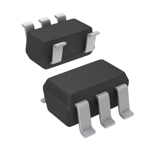
| 供应商器件封装 | SOT-23-5 |
| 偏转电压—最大值 | 7 mV |
| 元件数 | 1 |
| 其它名称 | 296-26111-1 |
| 包装 | 剪切带 (CT) |
| 单位重量 | 15.800 mg |
| 响应时间 | 0.2 us |
| 商标 | Texas Instruments |
| 安装类型 | 表面贴装 |
| 安装风格 | SMD/SMT |
| 封装 | Reel |
| 封装/外壳 | SC-74A,SOT-753 |
| 封装/箱体 | SOT-23-5 |
| 工作温度 | -40°C ~ 85°C |
| 工厂包装数量 | 250 |
| 最大工作温度 | + 125 C |
| 最小工作温度 | - 40 C |
| 标准包装 | 1 |
| 比较器类型 | General Purpose |
| 滞后 | - |
| 电压-电源,单/双 (±) | 2.7 V ~ 5.5 V |
| 电压-输入失调(最大值) | 7mV @ 5V |
| 电压增益dB | 93.98 dB |
| 电流-输入偏置(最大值) | 0.25µA @ 5V |
| 电流-输出(典型值) | 84mA @ 5V |
| 电流-静态(最大值) | 150µA |
| 电源电压-最大 | 5.5 V |
| 电源电压-最小 | 2.7 V |
| 电源电流 | 120 uA |
| 电源电流—最大值 | 120 uA |
| 类型 | 通用 |
| 系列 | LMV331 |
| 设计资源 | http://www.digikey.com/product-highlights/cn/zh/texas-instruments-webench-design-center/3176 |
| 输入偏压电流—最大 | 250 nA |
| 输出电流—典型值 | 10 mA |
| 输出类型 | 开路集电极 |
| 通道数量 | 1 Channel |


- 商务部:美国ITC正式对集成电路等产品启动337调查
- 曝三星4nm工艺存在良率问题 高通将骁龙8 Gen1或转产台积电
- 太阳诱电将投资9.5亿元在常州建新厂生产MLCC 预计2023年完工
- 英特尔发布欧洲新工厂建设计划 深化IDM 2.0 战略
- 台积电先进制程称霸业界 有大客户加持明年业绩稳了
- 达到5530亿美元!SIA预计今年全球半导体销售额将创下新高
- 英特尔拟将自动驾驶子公司Mobileye上市 估值或超500亿美元
- 三星加码芯片和SET,合并消费电子和移动部门,撤换高东真等 CEO
- 三星电子宣布重大人事变动 还合并消费电子和移动部门
- 海关总署:前11个月进口集成电路产品价值2.52万亿元 增长14.8%


PDF Datasheet 数据手册内容提取
Product Sample & Technical Tools & Support & Folder Buy Documents Software Community LMV331,LMV393,LMV339 SLCS136T–AUGUST1999–REVISEDJANUARY2015 LMV331 Single, LMV393 Dual, LMV339 Quad General-purpose Low-voltage Comparators 1 Features 3 Description • 2.7-Vand5-VPerformance The LMV393 and LMV339 devices are low-voltage 1 (2.7 V to 5.5 V) versions of the dual and quad • LowSupplyCurrent comparators, LM393 and LM339, which operate from – LMV331130μATyp 5 V to 30 V. The LMV331 is the single-comparator – LMV393210μATyp version. – LMV339410μATyp The LMV331, LMV339, and LMV393 are the most • InputCommon-ModeVoltageRangeIncludes cost-effective solutions for applications where low- voltage operation, low power, and space saving are Ground theprimaryspecificationsincircuitdesignforportable • LowOutputSaturationVoltage200mVTypical consumer products. These devices offer • Open-CollectorOutputforMaximumFlexibility specifications that meet or exceed the familiar LM339 andLM393devicesatafractionofthesupplycurrent. 2 Applications DeviceInformation(1) • HysteresisComparators PARTNUMBER PACKAGE(PIN) BODYSIZE(NOM) • Oscillators LMV339 SOIC(14) 8.65mmx3.90mm • WindowComparators LMV393 SOIC(8) 4.90mmx3.90mm • IndustrialEquipment LMV331 SC70(5) 2.00mmx1.25mm • TestandMeasurement (1) For all available packages, see the orderable addendum at theendofthedatasheet. 4 Simplified Schematic IN– – OUT IN+ + 1 An IMPORTANT NOTICE at the end of this data sheet addresses availability, warranty, changes, use in safety-critical applications, intellectualpropertymattersandotherimportantdisclaimers.PRODUCTIONDATA.
LMV331,LMV393,LMV339 SLCS136T–AUGUST1999–REVISEDJANUARY2015 www.ti.com Table of Contents 1 Features.................................................................. 1 8.1 Overview ..................................................................9 2 Applications........................................................... 1 8.2 FunctionalBlockDiagram.........................................9 3 Description............................................................. 1 8.3 FeatureDescription...................................................9 8.4 DeviceFunctionalModes..........................................9 4 SimplifiedSchematic............................................. 1 9 ApplicationandImplementation........................ 10 5 RevisionHistory..................................................... 2 9.1 ApplicationInformation............................................10 6 PinConfigurationandFunctions......................... 3 9.2 TypicalApplication .................................................10 7 Specifications......................................................... 4 10 PowerSupplyRecommendations..................... 12 7.1 AbsoluteMaximumRatings......................................4 11 Layout................................................................... 12 7.2 ESDRatings..............................................................4 11.1 LayoutGuidelines.................................................12 7.3 RecommendedOperatingConditions.......................4 11.2 LayoutExample....................................................12 7.4 ThermalInformation..................................................4 12 DeviceandDocumentationSupport................. 13 7.5 ElectricalCharacteristics,V =2.7V....................5 CC+ 7.6 ElectricalCharacteristics,V =5V.......................6 12.1 RelatedLinks........................................................13 CC+ 7.7 SwitchingCharacteristics,V =2.7V...................6 12.2 Trademarks...........................................................13 CC+ 7.8 SwitchingCharacteristics,V =5V......................6 12.3 ElectrostaticDischargeCaution............................13 CC+ 7.9 TypicalCharacteristics..............................................7 12.4 Glossary................................................................13 8 DetailedDescription.............................................. 9 13 Mechanical,Packaging,andOrderable Information........................................................... 13 5 Revision History ChangesfromRevisionS(October2012)toRevisionT Page • AddedApplications,DeviceInformationtable,PinFunctionstable,ESDRatingstable,ThermalInformationtable, TypicalCharacteristics,FeatureDescriptionsection,DeviceFunctionalModes,ApplicationandImplementation section,PowerSupplyRecommendationssection,Layoutsection,DeviceandDocumentationSupportsection,and Mechanical,Packaging,andOrderableInformationsection.................................................................................................. 1 • DeletedOrderingInformationtable........................................................................................................................................ 1 ChangesfromRevisionR(May2012)toRevisionS Page • Updatedoperatingtemperaturerange................................................................................................................................... 4 ChangesfromRevisionN(April2011)toRevisionO Page • ChangedV intheAbsoluteMaximumRatingsfrom5.5VtoV ....................................................................................... 4 I CC+ ChangesfromRevisionM(November2005)toRevisionN Page • ChangeddocumentformatfromQuicksilvertoDocZone...................................................................................................... 1 • AddedRUCpackagepinoutdrawing.................................................................................................................................... 3 2 SubmitDocumentationFeedback Copyright©1999–2015,TexasInstrumentsIncorporated
LMV331,LMV393,LMV339 www.ti.com SLCS136T–AUGUST1999–REVISEDJANUARY2015 6 Pin Configuration and Functions LMV339. . . D OR PW PACKAGE LMV339. . . RUC PACKAGE (TOPVIEW) (TOPVIEW) T T U U 2OUT 1 14 3OUT O O 2 3 1OUT 2 13 4OUT VCC+ 3 12 GND 1OUT 1 14 13 12 4OUT 1IN– 4 11 4IN+ VCC+ 2 11 GND 1IN+ 5 10 4IN– 1IN– 3 10 4IN+ 2IN– 6 9 3IN+ 2IN+ 7 8 3IN– 1IN+ 4 9 4IN– 2IN– 5 6 7 8 3IN+ + – N N 2I 3I LMV393 . . . D, DDU, DGK OR PW PACKAGE LMV331 . . . DBV OR DCK PACKAGE (TOPVIEW) (TOPVIEW) 1IN+ 1 5 V 1OUT 1 8 VCC+ CC+ 1IN– 2 7 2OUT GND 2 1IN+ 3 6 2IN– 1IN– 3 4 OUT GND 4 5 2IN+ PinFunctions PIN LMV331 LMV393 LMV339 TYPE DESCRIPTION NAME DBVor D,DDU, DorPW RUC DCK DGKorPW 1IN–, 2IN–, 3 2,6 4,6,8,10 3,5,7,9 I Comparator(s)negativeinputpin(s) 3IN–, 4IN– 1IN+, 2IN+, 1 3,5 5,7,9,11 4,6,8,10 I Comparator(s)positiveinputpin(s) 3IN+, 4IN+ GND 2 4 12 11 I Ground 1OUT, 2OUT, 4 1,7 2,1,14,13 1,14,13,12 O Comparator(s)outputpin(s) 3OUT, 4OUT V 5 8 3 2 I SupplyPin CC+ Copyright©1999–2015,TexasInstrumentsIncorporated SubmitDocumentationFeedback 3
LMV331,LMV393,LMV339 SLCS136T–AUGUST1999–REVISEDJANUARY2015 www.ti.com 7 Specifications 7.1 Absolute Maximum Ratings overoperatingfree-airtemperaturerange(unlessotherwisenoted)(1) MIN MAX UNIT V Supplyvoltage(2) 5.5 V CC V Differentialinputvoltage(3) ±5.5 V ID V Inputvoltagerange(eitherinput) 0 V V I CC+ Durationofoutputshortcircuit(oneamplifier)toground(4) AtorbelowTA=25°C, Unlimited V ≤5.5V CC T Operatingvirtualjunctiontemperature 150 °C J T Storagetemperaturerange –65 150 °C stg (1) StressesbeyondthoselistedunderAbsoluteMaximumRatingsmaycausepermanentdamagetothedevice.Thesearestressratings only,andfunctionaloperationofthedeviceattheseoranyotherconditionsbeyondthoseindicatedunderRecommendedOperating Conditionsisnotimplied.Exposuretoabsolute-maximum-ratedconditionsforextendedperiodsmayaffectdevicereliability. (2) Allvoltagevalues(exceptdifferentialvoltagesandV specifiedforthemeasurementofI )arewithrespecttothenetworkGND. CC OS (3) DifferentialvoltagesareatIN+withrespecttoIN–. (4) ShortcircuitsfromoutputstoV cancauseexcessiveheatingandeventualdestruction. CC 7.2 ESD Ratings VALUE UNIT Humanbodymodel(HBM),perANSI/ESDA/JEDECJS-001,allpins(1) ±2000 V(ESD) Electrostaticdischarge Chargeddevicemodel(CDM),perJEDECspecificationJESD22-C101, V allpins(2) ±1000 (1) JEDECdocumentJEP155statesthat500-VHBMallowssafemanufacturingwithastandardESDcontrolprocess. (2) JEDECdocumentJEP157statesthat250-VCDMallowssafemanufacturingwithastandardESDcontrolprocess. 7.3 Recommended Operating Conditions MIN MAX UNIT V Supplyvoltage(single-supplyoperation) 2.7 5.5 V CC V Outputvoltage V +0.3 V OUT CC+ T Operatingfree-airtemperature –40 125 °C A 7.4 Thermal Information LMV339 LMV393 LMV331 THERMALMETRIC(1) D PW RUC D DDU DGK PW DBV DCK UNIT 14PINS 8PINS 5PINS RθJA Junction-to-ambient 86 113 216 97 210 172 149 206 252 thermalresistance RθJC(top) Junction-to-case(top) — — 51.3 — — — — — — thermalresistance RθJB Junction-to-board — — 59.0 — — — — — — thermalresistance °C/W ψJT Junction-to-top characterization — — 1.2 — — — — — — parameter ψJB Junction-to-board characterization — — 59.0 — — — — — — parameter (1) Formoreinformationabouttraditionalandnewthermalmetrics,seetheICPackageThermalMetricsapplicationreport,SPRA953. 4 SubmitDocumentationFeedback Copyright©1999–2015,TexasInstrumentsIncorporated
LMV331,LMV393,LMV339 www.ti.com SLCS136T–AUGUST1999–REVISEDJANUARY2015 7.5 Electrical Characteristics, V = 2.7 V CC+ V =2.7V,GND=0V,atspecifiedfree-airtemperature(unlessotherwisenoted) CC+ PARAMETER TESTCONDITIONS T MIN TYP MAX UNIT A V Inputoffsetvoltage 25°C 1.7 7 mV IO Averagetemperature –40°Cto α coefficientofinputoffset 5 μV/°C VIO 125°C voltage 25°C 15 250 IIB Inputbiascurrent –40°Cto nA 400 125°C 25°C 5 50 IIO Inputoffsetcurrent –40°Cto nA 150 125°C I Outputcurrent(sinking) V ≤1.5V 25°C 5 23 mA O O 25°C 0.003 OutputLeakageCurrent –40°Cto µA 1 125°C Common-modeinput V 25°C –0.1to2 V ICR voltagerange V Saturationvoltage I ≤1.5mA 25°C 200 mV SAT O LMV331 25°C 40 100 I Supplycurrent LMV393(bothcomparators) 25°C 70 140 μA CC LMV339(allfourcomparators) 25°C 140 200 Copyright©1999–2015,TexasInstrumentsIncorporated SubmitDocumentationFeedback 5
LMV331,LMV393,LMV339 SLCS136T–AUGUST1999–REVISEDJANUARY2015 www.ti.com 7.6 Electrical Characteristics, V = 5 V CC+ V =5V,GND=0V,atspecifiedfree-airtemperature(unlessotherwisenoted) CC+ PARAMETER TESTCONDITIONS T MIN TYP MAX UNIT A 25°C 1.7 7 VIO Inputoffsetvoltage –40°Cto mV 9 125°C Averagetemperature α coefficientofinputoffset 25°C 5 μV/°C VIO voltage 25°C 25 250 IIB Inputbiascurrent –40°Cto nA 400 125°C 25°C 2 50 IIO Inputoffsetcurrent –40°Cto nA 150 125°C I Outputcurrent(sinking) V ≤1.5V 25°C 10 84 mA O O 25°C 0.003 OutputLeakageCurrent –40°Cto µA 1 125°C Common-modeinput V 25°C –0.1to4.2 V ICR voltagerange Large-signaldifferential A 25°C 20 50 V/mV VD voltagegain 25°C 200 400 VSAT Saturationvoltage IO≤4mA –40°Cto mV 700 125°C 25°C 60 120 LMV331 –40°Cto 150 125°C 25°C 100 200 ICC Supplycurrent LMV393(bothcomparators) –40°Cto μA 250 125°C 25°C 170 300 LMV339(allfourcomparators) –40°Cto 350 125°C 7.7 Switching Characteristics, V = 2.7 V CC+ T =25°C,V =2.7V,R =5.1kΩ,GND=0V(unlessotherwisenoted) A CC+ L PARAMETER TESTCONDITIONS TYP UNIT Propagationdelayhightolowleveloutput Inputoverdrive=10mV 1000 t ns PHL switching Inputoverdrive=100mV 350 Propagationdelaylowtohighleveloutput Inputoverdrive=10mV 500 t ns PLH switching Inputoverdrive=100mV 400 7.8 Switching Characteristics, V = 5 V CC+ T =25°C,V =5V,R =5.1kΩ,GND=0V(unlessotherwisenoted) A CC+ L PARAMETER TESTCONDITIONS TYP UNIT Propagationdelayhightolowleveloutput Inputoverdrive=10mV 600 t ns PHL switching Inputoverdrive=100mV 200 Propagationdelaylowtohighleveloutput Inputoverdrive=10mV 450 t ns PLH switching Inputoverdrive=100mV 300 6 SubmitDocumentationFeedback Copyright©1999–2015,TexasInstrumentsIncorporated
LMV331,LMV393,LMV339 www.ti.com SLCS136T–AUGUST1999–REVISEDJANUARY2015 7.9 Typical Characteristics Unlessotherwisespecified,VS=+5V,singlesupply,TA=25°C 70 95 65 -40C 90 -40C 25C 25C 60 85 85C 85C 55 80 A) 50 A) 75 P P ent ( 4405 ent ( 6750 urr 35 urr 60 C C y 30 y 55 pl pl p 25 p 50 p p Su 20 Su 45 15 40 10 35 5 30 0 25 1 1.5 2 2.5 3 3.5 4 4.5 5 1 1.5 2 2.5 3 3.5 4 4.5 5 Volts (V) Volts (V) Figure1.SupplyCurrentvsSupplyVoltageOutputHigh Figure2.SupplyCurrentvsSupplyVoltageOutputLow (LMV33x) (LMV33x) 700 55 650 -40C 52.5 -40C 25C 25C 600 85C 50 85C V) 550 nA) 47.5 e (m 455000 ent ( 424.55 Voltag 400 s Curr 40 ut 350 Bia 37.5 utp 300 ut 35 O p 250 n 32.5 I 200 30 150 27.5 100 25 0 5 10 15 20 25 30 35 40 45 50 2.4 2.7 3 3.3 3.6 3.9 4.2 4.5 4.8 5.1 5.4 5.7 Output Current (mA) Supply Voltage (V) Figure3.OutputVoltagevsOutputCurrent Figure4.InputBiasCurrentvsSupplyVoltage 310 176.1 175.8 305 175.5 300 175.2 295 174.9 ns) 290 ns) 174.6 e ( e ( 174.3 m 285 m Ti Ti 174 280 173.7 173.4 275 173.1 270 172.8 265 172.5 0 10 20 30 40 50 60 70 80 90 100 0 10 20 30 40 50 60 70 80 90 100 Overdrive (mV) Overdrive (mV) Figure5.ResponseTimevsInputOverdrivesNegative Figure6.ResponseTimevsInputOverdrivesPositive Transition(V =5V) Transition(V =5V) CC CC Copyright©1999–2015,TexasInstrumentsIncorporated SubmitDocumentationFeedback 7
LMV331,LMV393,LMV339 SLCS136T–AUGUST1999–REVISEDJANUARY2015 www.ti.com Typical Characteristics (continued) Unlessotherwisespecified,VS=+5V,singlesupply,TA=25°C 648 189 645 188.7 642 188.4 639 188.1 636 187.8 s) 633 s) 187.5 n n e ( 630 e ( 187.2 m m Ti 627 Ti 186.9 624 186.6 621 186.3 618 186 615 185.7 612 185.4 0 10 20 30 40 50 60 70 80 90 100 0 10 20 30 40 50 60 70 80 90 100 Overdrive (mV) Overdrive (mV) Figure7.ResponseTimevsInputOverdrivesNegative Figure8.ResponseTimevsInputOverdrivesPositive Transition(V =2.7V) Transition(V =2.7V) CC CC 8 SubmitDocumentationFeedback Copyright©1999–2015,TexasInstrumentsIncorporated
LMV331,LMV393,LMV339 www.ti.com SLCS136T–AUGUST1999–REVISEDJANUARY2015 8 Detailed Description 8.1 Overview TheLMV331,LMV393andLMV339familyofcomparatorshavetheabilitytooperateupto5Vonthesupplypin. This standard device has proven ubiquity and versatility across a wide range of applications. This is due to it's lowIqandfastresponse. The open-drain output allows the user to configure the output's logic low voltage (V ) and can be utilized to OL enablethecomparatortobeusedinANDfunctionality. 8.2 Functional Block Diagram V CC+ Q6 Q7 Q8 OUT IN+ Q1 Q2 Q3 Q4 Q5 Q9 IN− R1 R2 R3 GND 8.3 Feature Description The LMV331, LMV393 and LMV339 consists of a PNP input, whose Vbe creates a limit on the input common mode voltage capability, allowing LMV33x to accurately function from ground to V –Vbe(~700mV) differential CC input.Thisenablesmuchheadroomformoderndaysuppliesof3.3Vand5.0V. The output consists of an open drain NPN (pull-down or low side) transistor. The output NPN will sink current when the positive input voltage is higher than the negative input voltage and the offset voltage. The V is OL resistive and will scale with the output current. Please see Figure 3 for V values with respect to the output OL current. 8.4 Device Functional Modes 8.4.1 VoltageComparison The LMV33x operates solely as a voltage comparator, comparing the differential voltage between the positive and negative pins and outputs a logic low or high impedance (logic high with pull-up) based on the input differentialpolarity. Copyright©1999–2015,TexasInstrumentsIncorporated SubmitDocumentationFeedback 9
LMV331,LMV393,LMV339 SLCS136T–AUGUST1999–REVISEDJANUARY2015 www.ti.com 9 Application and Implementation NOTE Information in the following applications sections is not part of the TI component specification, and TI does not warrant its accuracy or completeness. TI’s customers are responsible for determining suitability of components for their purposes. Customers should validateandtesttheirdesignimplementationtoconfirmsystemfunctionality. 9.1 Application Information LMV331, LMV393, and LMV339 will typically be used to compare a single signal to a reference or two signals againsteachother.Manyuserstakeadvantageoftheopendrainoutputtodrivethecomparisonlogicoutputtoa logic voltage level to an MCU or logic device. The wide supply range and high voltage capability makes LMV331, LMV393,andLMV33optimalforlevelshiftingtoahigherorlowervoltage. 9.2 Typical Application V V LOGIC LOGIC V V SUP Rpullup SUP Rpullup Vin + Vin+ + LMV33x LMV33x Vref Vin- C C L L Figure9. TypicalApplicationSchematic 9.2.1 DesignRequirements Forthisdesignexample,usetheparameterslistedinTable1astheinputparameters. Table1.DesignParameters DESIGNPARAMETER EXAMPLEVALUE InputVoltageRange 0Vto4.2V SupplyVoltage 2.7Vto5V LogicSupplyVoltage(R Voltage) 1Vto5V PULLUP OutputCurrent(V /R ) 1µAto20mA LOGIC PULLUP InputOverdriveVoltage 100mV ReferenceVoltage 2.5V LoadCapacitance(C ) 15pF L 9.2.2 DetailedDesignProcedure WhenusingLMV331,LMV393,andLMV33inageneralcomparatorapplication,determinethefollowing: • InputVoltageRange • MinimumOverdriveVoltage • OutputandDriveCurrent • ResponseTime 10 SubmitDocumentationFeedback Copyright©1999–2015,TexasInstrumentsIncorporated
LMV331,LMV393,LMV339 www.ti.com SLCS136T–AUGUST1999–REVISEDJANUARY2015 9.2.2.1 InputVoltageRange When choosing the input voltage range, the input common mode voltage range (V ) must be taken in to ICR account. If operating temperature is above or below 25°C the V can range from 0 V to V – 0.7 V. This limits ICR CC the input voltage range to as high as V – 0.7 V and as low as 0 V. Operation outside of this range can yield CC incorrectcomparisons. Belowisapossiblelistofinputvoltagesituationandtheiroutcomes: 1. WhenbothIN-andIN+arebothwithinthecommonmoderange: (a) If IN- is higher than IN+ and the offset voltage, the output is low and the output transistor is sinking current (b) If IN- is lower than IN+ and the offset voltage, the output is high impedance and the output transistor is notconducting 2. When IN- is higher than common mode and IN+ is within common mode, the output is low and the output transistorissinkingcurrent 3. When IN+ is higher than common mode and IN- is within common mode, the output is high impedance and theoutputtransistorisnotconducting 4. When IN- and IN+ are both higher than common mode, the output is low and the output transistor is sinking current 9.2.2.2 MinimumOverdriveVoltage OverdriveVoltageisthedifferentialvoltageproducedbetweenthepositiveandnegativeinputsofthecomparator over the offset voltage (V ). In order to make an accurate comparison; the Overdrive Voltage (V ) should be IO OD higher than the input offset voltage (V ). Overdrive voltage can also determine the response time of the IO comparator, with the response time decreasing with increasing overdrive. Figure 10 show positive and negative responsetimeswithrespecttooverdrivevoltage. 9.2.2.3 OutputandDriveCurrent Output current is determined by the pull-up resistance (Rpullup) and Vlogic voltage, refer to Figure 9. The output current will produce a output low voltage (V ) from the comparator. In which V is proportional to the output OL OL current.UseFigure3todetermineV basedontheoutputcurrent. OL Theoutputcurrentcanalsoeffectthetransientresponse.Morewillbeexplainedinthenextsection. 9.2.2.4 ResponseTime The transient response can be determined by the load capacitance (C ), load/pull-up resistance (R ) and L PULLUP equivalentcollector-emitterresistance(R ). CE • Thepositiveresponsetime(τ )isapproximatelyτ ~R ×C p P PULLUP L • Thenegativeresponsetime(τ )isapproximatelyτ ~R ×C N N CE L – R can be determine by taking the slope of Figure 3 in it's linear region at the desired temperature, or by CE dividingtheV byI OL out 9.2.3 ApplicationCurves Thefollowingcurvesweregeneratedwith5VonV andV ,R =5.1kΩ,and50pFscopeprobe. CC Logic PULLUP Copyright©1999–2015,TexasInstrumentsIncorporated SubmitDocumentationFeedback 11
LMV331,LMV393,LMV339 SLCS136T–AUGUST1999–REVISEDJANUARY2015 www.ti.com 6 5.5 5 5mV OD 4.5 20mV OD 100mV OD 4 3.5 ge (V) 2.53 a olt 2 V 1.5 1 0.5 0 -0.5 -1 0.2 0.22 0.24 0.26 0.28 0.3 0.32 0.34 0.36 0.38 0.4 Time (uS) Figure10.ResponseTimeforVariousOverdrives (NegativeTransition) 10 Power Supply Recommendations For fast response and comparison applications with noisy or AC inputs, it is recommended to use a bypass capacitor on the supply pin to reject any variation on the supply voltage. This variation cause temporary fluctuationsinthecomparator'sinputcommonmoderangeandcreateaninaccuratecomparison. 11 Layout 11.1 Layout Guidelines For accurate comparator applications without hysteresis it is important maintain a stable power supply with minimized noise and glitches, which can affect the high level input common mode voltage range. In order to achieve this, it is best to add a bypass capacitor between the supply voltage and ground. This should be implemented on the positive power supply and negative supply (if available). If a negative supply is not being used,donotputacapacitorbetweentheIC'sGNDpinandsystemground. 11.2 Layout Example Ground Bypass Capacitor 0.1μF IN– 1 5 VCC Positive Supply Negative Supply or Ground GND 2 Only needed IN+ 3 4 OUT for dual power 0.1μF supplies Ground Figure11. LMV331LayoutExample 12 SubmitDocumentationFeedback Copyright©1999–2015,TexasInstrumentsIncorporated
LMV331,LMV393,LMV339 www.ti.com SLCS136T–AUGUST1999–REVISEDJANUARY2015 12 Device and Documentation Support 12.1 Related Links The table below lists quick access links. Categories include technical documents, support and community resources,toolsandsoftware,andquickaccesstosampleorbuy. Table2.RelatedLinks TECHNICAL TOOLS& SUPPORT& PARTS PRODUCTFOLDER SAMPLE&BUY DOCUMENTS SOFTWARE COMMUNITY LMV331 Clickhere Clickhere Clickhere Clickhere Clickhere LMV393 Clickhere Clickhere Clickhere Clickhere Clickhere LMV339 Clickhere Clickhere Clickhere Clickhere Clickhere 12.2 Trademarks Alltrademarksarethepropertyoftheirrespectiveowners. 12.3 Electrostatic Discharge Caution Thesedeviceshavelimitedbuilt-inESDprotection.Theleadsshouldbeshortedtogetherorthedeviceplacedinconductivefoam duringstorageorhandlingtopreventelectrostaticdamagetotheMOSgates. 12.4 Glossary SLYZ022—TIGlossary. Thisglossarylistsandexplainsterms,acronyms,anddefinitions. 13 Mechanical, Packaging, and Orderable Information The following pages include mechanical, packaging, and orderable information. This information is the most current data available for the designated devices. This data is subject to change without notice and revision of thisdocument.Forbrowser-basedversionsofthisdatasheet,refertotheleft-handnavigation. Copyright©1999–2015,TexasInstrumentsIncorporated SubmitDocumentationFeedback 13
PACKAGE OPTION ADDENDUM www.ti.com 24-Aug-2018 PACKAGING INFORMATION Orderable Device Status Package Type Package Pins Package Eco Plan Lead/Ball Finish MSL Peak Temp Op Temp (°C) Device Marking Samples (1) Drawing Qty (2) (6) (3) (4/5) LMV331IDBVR ACTIVE SOT-23 DBV 5 3000 Green (RoHS CU NIPDAU Level-1-260C-UNLIM -40 to 125 (R1IC, R1II) & no Sb/Br) LMV331IDBVRE4 ACTIVE SOT-23 DBV 5 3000 Green (RoHS CU NIPDAU Level-1-260C-UNLIM -40 to 125 (R1IC, R1II) & no Sb/Br) LMV331IDBVRG4 ACTIVE SOT-23 DBV 5 3000 Green (RoHS CU NIPDAU Level-1-260C-UNLIM -40 to 125 (R1IC, R1II) & no Sb/Br) LMV331IDBVT ACTIVE SOT-23 DBV 5 250 Green (RoHS CU NIPDAU Level-1-260C-UNLIM -40 to 125 (R1IC, R1II) & no Sb/Br) LMV331IDBVTG4 ACTIVE SOT-23 DBV 5 250 Green (RoHS CU NIPDAU Level-1-260C-UNLIM -40 to 125 (R1IC, R1II) & no Sb/Br) LMV331IDCKR ACTIVE SC70 DCK 5 3000 Green (RoHS CU NIPDAU | Level-1-260C-UNLIM -40 to 125 (R2I, R2K, R2R) & no Sb/Br) CU NIPDAUAG LMV331IDCKRE4 ACTIVE SC70 DCK 5 3000 Green (RoHS CU NIPDAU Level-1-260C-UNLIM -40 to 125 (R2I, R2K, R2R) & no Sb/Br) LMV331IDCKRG4 ACTIVE SC70 DCK 5 3000 Green (RoHS CU NIPDAU Level-1-260C-UNLIM -40 to 125 (R2I, R2K, R2R) & no Sb/Br) LMV331IDCKT ACTIVE SC70 DCK 5 250 Green (RoHS CU NIPDAU | Level-1-260C-UNLIM -40 to 125 (R2C, R2I, R2R) & no Sb/Br) CU NIPDAUAG LMV331IDCKTE4 ACTIVE SC70 DCK 5 250 Green (RoHS CU NIPDAU Level-1-260C-UNLIM -40 to 125 (R2C, R2I, R2R) & no Sb/Br) LMV331IDCKTG4 ACTIVE SC70 DCK 5 250 Green (RoHS CU NIPDAU Level-1-260C-UNLIM -40 to 125 (R2C, R2I, R2R) & no Sb/Br) LMV339ID ACTIVE SOIC D 14 50 Green (RoHS CU NIPDAU Level-1-260C-UNLIM -40 to 125 LMV339I & no Sb/Br) LMV339IDR ACTIVE SOIC D 14 2500 Green (RoHS CU NIPDAU Level-1-260C-UNLIM -40 to 125 LMV339I & no Sb/Br) LMV339IPW ACTIVE TSSOP PW 14 90 Green (RoHS CU NIPDAU Level-1-260C-UNLIM -40 to 125 MV339I & no Sb/Br) LMV339IPWR ACTIVE TSSOP PW 14 2000 Green (RoHS CU NIPDAU Level-1-260C-UNLIM -40 to 125 MV339I & no Sb/Br) LMV339IPWRE4 ACTIVE TSSOP PW 14 2000 Green (RoHS CU NIPDAU Level-1-260C-UNLIM -40 to 125 MV339I & no Sb/Br) LMV339IPWRG4 ACTIVE TSSOP PW 14 2000 Green (RoHS CU NIPDAU Level-1-260C-UNLIM -40 to 125 MV339I & no Sb/Br) Addendum-Page 1
PACKAGE OPTION ADDENDUM www.ti.com 24-Aug-2018 Orderable Device Status Package Type Package Pins Package Eco Plan Lead/Ball Finish MSL Peak Temp Op Temp (°C) Device Marking Samples (1) Drawing Qty (2) (6) (3) (4/5) LMV339IRUCR ACTIVE QFN RUC 14 3000 Green (RoHS CU NIPDAUAG Level-1-260C-UNLIM -40 to 125 (RT, RTR) & no Sb/Br) LMV393ID ACTIVE SOIC D 8 75 Green (RoHS CU NIPDAU Level-1-260C-UNLIM -40 to 125 MV393I & no Sb/Br) LMV393IDDUR ACTIVE VSSOP DDU 8 3000 Green (RoHS CU NIPDAU Level-1-260C-UNLIM -40 to 125 RABR & no Sb/Br) LMV393IDDURG4 ACTIVE VSSOP DDU 8 3000 Green (RoHS CU NIPDAU Level-1-260C-UNLIM -40 to 125 RABR & no Sb/Br) LMV393IDGKR ACTIVE VSSOP DGK 8 2500 Green (RoHS CU NIPDAU | Level-1-260C-UNLIM -40 to 125 (R9B, R9Q, R9R) & no Sb/Br) CU NIPDAUAG LMV393IDGKRG4 ACTIVE VSSOP DGK 8 2500 Green (RoHS CU NIPDAUAG Level-1-260C-UNLIM -40 to 125 (R9B, R9Q, R9R) & no Sb/Br) LMV393IDR ACTIVE SOIC D 8 2500 Green (RoHS CU NIPDAU | CU SN Level-1-260C-UNLIM -40 to 125 MV393I & no Sb/Br) LMV393IDRG4 ACTIVE SOIC D 8 2500 Green (RoHS CU NIPDAU Level-1-260C-UNLIM -40 to 125 MV393I & no Sb/Br) LMV393IPW ACTIVE TSSOP PW 8 150 Green (RoHS CU NIPDAU Level-1-260C-UNLIM -40 to 125 MV393I & no Sb/Br) LMV393IPWG4 ACTIVE TSSOP PW 8 150 Green (RoHS CU NIPDAU Level-1-260C-UNLIM -40 to 125 MV393I & no Sb/Br) LMV393IPWR ACTIVE TSSOP PW 8 2000 Green (RoHS CU NIPDAU Level-1-260C-UNLIM -40 to 125 MV393I & no Sb/Br) LMV393IPWRG4 ACTIVE TSSOP PW 8 2000 Green (RoHS CU NIPDAU Level-1-260C-UNLIM -40 to 125 MV393I & no Sb/Br) (1) The marketing status values are defined as follows: ACTIVE: Product device recommended for new designs. LIFEBUY: TI has announced that the device will be discontinued, and a lifetime-buy period is in effect. NRND: Not recommended for new designs. Device is in production to support existing customers, but TI does not recommend using this part in a new design. PREVIEW: Device has been announced but is not in production. Samples may or may not be available. OBSOLETE: TI has discontinued the production of the device. (2) RoHS: TI defines "RoHS" to mean semiconductor products that are compliant with the current EU RoHS requirements for all 10 RoHS substances, including the requirement that RoHS substance do not exceed 0.1% by weight in homogeneous materials. Where designed to be soldered at high temperatures, "RoHS" products are suitable for use in specified lead-free processes. TI may reference these types of products as "Pb-Free". RoHS Exempt: TI defines "RoHS Exempt" to mean products that contain lead but are compliant with EU RoHS pursuant to a specific EU RoHS exemption. Green: TI defines "Green" to mean the content of Chlorine (Cl) and Bromine (Br) based flame retardants meet JS709B low halogen requirements of <=1000ppm threshold. Antimony trioxide based flame retardants must also meet the <=1000ppm threshold requirement. Addendum-Page 2
PACKAGE OPTION ADDENDUM www.ti.com 24-Aug-2018 (3) MSL, Peak Temp. - The Moisture Sensitivity Level rating according to the JEDEC industry standard classifications, and peak solder temperature. (4) There may be additional marking, which relates to the logo, the lot trace code information, or the environmental category on the device. (5) Multiple Device Markings will be inside parentheses. Only one Device Marking contained in parentheses and separated by a "~" will appear on a device. If a line is indented then it is a continuation of the previous line and the two combined represent the entire Device Marking for that device. (6) Lead/Ball Finish - Orderable Devices may have multiple material finish options. Finish options are separated by a vertical ruled line. Lead/Ball Finish values may wrap to two lines if the finish value exceeds the maximum column width. Important Information and Disclaimer:The information provided on this page represents TI's knowledge and belief as of the date that it is provided. TI bases its knowledge and belief on information provided by third parties, and makes no representation or warranty as to the accuracy of such information. Efforts are underway to better integrate information from third parties. TI has taken and continues to take reasonable steps to provide representative and accurate information but may not have conducted destructive testing or chemical analysis on incoming materials and chemicals. TI and TI suppliers consider certain information to be proprietary, and thus CAS numbers and other limited information may not be available for release. In no event shall TI's liability arising out of such information exceed the total purchase price of the TI part(s) at issue in this document sold by TI to Customer on an annual basis. OTHER QUALIFIED VERSIONS OF LMV331, LMV393 : •Automotive: LMV331-Q1, LMV393-Q1 NOTE: Qualified Version Definitions: •Automotive - Q100 devices qualified for high-reliability automotive applications targeting zero defects Addendum-Page 3
PACKAGE MATERIALS INFORMATION www.ti.com 3-Aug-2017 TAPE AND REEL INFORMATION *Alldimensionsarenominal Device Package Package Pins SPQ Reel Reel A0 B0 K0 P1 W Pin1 Type Drawing Diameter Width (mm) (mm) (mm) (mm) (mm) Quadrant (mm) W1(mm) LMV331IDBVR SOT-23 DBV 5 3000 178.0 9.0 3.23 3.17 1.37 4.0 8.0 Q3 LMV331IDBVT SOT-23 DBV 5 250 178.0 9.0 3.23 3.17 1.37 4.0 8.0 Q3 LMV331IDCKR SC70 DCK 5 3000 180.0 9.2 2.3 2.55 1.2 4.0 8.0 Q3 LMV331IDCKR SC70 DCK 5 3000 178.0 9.0 2.4 2.5 1.2 4.0 8.0 Q3 LMV331IDCKT SC70 DCK 5 250 180.0 9.2 2.3 2.55 1.2 4.0 8.0 Q3 LMV331IDCKT SC70 DCK 5 250 178.0 9.0 2.4 2.5 1.2 4.0 8.0 Q3 LMV339IDR SOIC D 14 2500 330.0 16.4 6.5 9.0 2.1 8.0 16.0 Q1 LMV339IPWR TSSOP PW 14 2000 330.0 12.4 6.9 5.6 1.6 8.0 12.0 Q1 LMV339IRUCR QFN RUC 14 3000 180.0 8.4 2.3 2.3 0.55 4.0 8.0 Q2 LMV393IDDUR VSSOP DDU 8 3000 180.0 8.4 2.25 3.35 1.05 4.0 8.0 Q3 LMV393IDGKR VSSOP DGK 8 2500 330.0 12.4 5.3 3.4 1.4 8.0 12.0 Q1 LMV393IDR SOIC D 8 2500 330.0 12.4 6.4 5.2 2.1 8.0 12.0 Q1 LMV393IDR SOIC D 8 2500 330.0 12.8 6.4 5.2 2.1 8.0 12.0 Q1 LMV393IDRG4 SOIC D 8 2500 330.0 12.4 6.4 5.2 2.1 8.0 12.0 Q1 LMV393IPWR TSSOP PW 8 2000 330.0 12.4 7.0 3.6 1.6 8.0 12.0 Q1 PackMaterials-Page1
PACKAGE MATERIALS INFORMATION www.ti.com 3-Aug-2017 *Alldimensionsarenominal Device PackageType PackageDrawing Pins SPQ Length(mm) Width(mm) Height(mm) LMV331IDBVR SOT-23 DBV 5 3000 180.0 180.0 18.0 LMV331IDBVT SOT-23 DBV 5 250 180.0 180.0 18.0 LMV331IDCKR SC70 DCK 5 3000 205.0 200.0 33.0 LMV331IDCKR SC70 DCK 5 3000 180.0 180.0 18.0 LMV331IDCKT SC70 DCK 5 250 205.0 200.0 33.0 LMV331IDCKT SC70 DCK 5 250 180.0 180.0 18.0 LMV339IDR SOIC D 14 2500 367.0 367.0 38.0 LMV339IPWR TSSOP PW 14 2000 367.0 367.0 35.0 LMV339IRUCR QFN RUC 14 3000 202.0 201.0 28.0 LMV393IDDUR VSSOP DDU 8 3000 202.0 201.0 28.0 LMV393IDGKR VSSOP DGK 8 2500 364.0 364.0 27.0 LMV393IDR SOIC D 8 2500 340.5 338.1 20.6 LMV393IDR SOIC D 8 2500 364.0 364.0 27.0 LMV393IDRG4 SOIC D 8 2500 340.5 338.1 20.6 LMV393IPWR TSSOP PW 8 2000 367.0 367.0 35.0 PackMaterials-Page2
None
None
None
None
None
None
PACKAGE OUTLINE D0008A SOIC - 1.75 mm max height SCALE 2.800 SMALL OUTLINE INTEGRATED CIRCUIT C SEATING PLANE .228-.244 TYP [5.80-6.19] .004 [0.1] C A PIN 1 ID AREA 6X .050 [1.27] 8 1 2X .189-.197 [4.81-5.00] .150 NOTE 3 [3.81] 4X (0 -15 ) 4 5 8X .012-.020 B .150-.157 [0.31-0.51] .069 MAX [3.81-3.98] .010 [0.25] C A B [1.75] NOTE 4 .005-.010 TYP [0.13-0.25] 4X (0 -15 ) SEE DETAIL A .010 [0.25] .004-.010 0 - 8 [0.11-0.25] .016-.050 [0.41-1.27] DETAIL A (.041) TYPICAL [1.04] 4214825/C 02/2019 NOTES: 1. Linear dimensions are in inches [millimeters]. Dimensions in parenthesis are for reference only. Controlling dimensions are in inches. Dimensioning and tolerancing per ASME Y14.5M. 2. This drawing is subject to change without notice. 3. This dimension does not include mold flash, protrusions, or gate burrs. Mold flash, protrusions, or gate burrs shall not exceed .006 [0.15] per side. 4. This dimension does not include interlead flash. 5. Reference JEDEC registration MS-012, variation AA. www.ti.com
EXAMPLE BOARD LAYOUT D0008A SOIC - 1.75 mm max height SMALL OUTLINE INTEGRATED CIRCUIT 8X (.061 ) [1.55] SYMM SEE DETAILS 1 8 8X (.024) [0.6] SYMM (R.002 ) TYP [0.05] 5 4 6X (.050 ) [1.27] (.213) [5.4] LAND PATTERN EXAMPLE EXPOSED METAL SHOWN SCALE:8X SOLDER MASK SOLDER MASK METAL OPENING OPENING METAL UNDER SOLDER MASK EXPOSED METAL EXPOSED METAL .0028 MAX .0028 MIN [0.07] [0.07] ALL AROUND ALL AROUND NON SOLDER MASK SOLDER MASK DEFINED DEFINED SOLDER MASK DETAILS 4214825/C 02/2019 NOTES: (continued) 6. Publication IPC-7351 may have alternate designs. 7. Solder mask tolerances between and around signal pads can vary based on board fabrication site. www.ti.com
EXAMPLE STENCIL DESIGN D0008A SOIC - 1.75 mm max height SMALL OUTLINE INTEGRATED CIRCUIT 8X (.061 ) [1.55] SYMM 1 8 8X (.024) [0.6] SYMM (R.002 ) TYP [0.05] 5 4 6X (.050 ) [1.27] (.213) [5.4] SOLDER PASTE EXAMPLE BASED ON .005 INCH [0.125 MM] THICK STENCIL SCALE:8X 4214825/C 02/2019 NOTES: (continued) 8. Laser cutting apertures with trapezoidal walls and rounded corners may offer better paste release. IPC-7525 may have alternate design recommendations. 9. Board assembly site may have different recommendations for stencil design. www.ti.com
PACKAGE OUTLINE DBV0005A SOT-23 - 1.45 mm max height SCALE 4.000 SMALL OUTLINE TRANSISTOR C 3.0 2.6 0.1 C 1.75 1.45 B A 1.45 MAX PIN 1 INDEX AREA 1 5 2X 0.95 3.05 2.75 1.9 1.9 2 4 3 0.5 5X 0.3 0.15 0.2 C A B (1.1) TYP 0.00 0.25 GAGE PLANE 0.22 TYP 0.08 8 TYP 0.6 0 0.3 TYP SEATING PLANE 4214839/D 11/2018 NOTES: 1. All linear dimensions are in millimeters. Any dimensions in parenthesis are for reference only. Dimensioning and tolerancing per ASME Y14.5M. 2. This drawing is subject to change without notice. 3. Refernce JEDEC MO-178. 4. Body dimensions do not include mold flash, protrusions, or gate burrs. Mold flash, protrusions, or gate burrs shall not exceed 0.15 mm per side. www.ti.com
EXAMPLE BOARD LAYOUT DBV0005A SOT-23 - 1.45 mm max height SMALL OUTLINE TRANSISTOR PKG 5X (1.1) 1 5 5X (0.6) SYMM (1.9) 2 2X (0.95) 3 4 (R0.05) TYP (2.6) LAND PATTERN EXAMPLE EXPOSED METAL SHOWN SCALE:15X SOLDER MASK SOLDER MASK METAL UNDER METAL OPENING OPENING SOLDER MASK EXPOSED METAL EXPOSED METAL 0.07 MAX 0.07 MIN ARROUND ARROUND NON SOLDER MASK SOLDER MASK DEFINED DEFINED (PREFERRED) SOLDER MASK DETAILS 4214839/D 11/2018 NOTES: (continued) 5. Publication IPC-7351 may have alternate designs. 6. Solder mask tolerances between and around signal pads can vary based on board fabrication site. www.ti.com
EXAMPLE STENCIL DESIGN DBV0005A SOT-23 - 1.45 mm max height SMALL OUTLINE TRANSISTOR PKG 5X (1.1) 1 5 5X (0.6) SYMM 2 (1.9) 2X(0.95) 3 4 (R0.05) TYP (2.6) SOLDER PASTE EXAMPLE BASED ON 0.125 mm THICK STENCIL SCALE:15X 4214839/D 11/2018 NOTES: (continued) 7. Laser cutting apertures with trapezoidal walls and rounded corners may offer better paste release. IPC-7525 may have alternate design recommendations. 8. Board assembly site may have different recommendations for stencil design. www.ti.com
None
None
PACKAGE OUTLINE PW0008A TSSOP - 1.2 mm max height SCALE 2.800 SMALL OUTLINE PACKAGE C 6.6 TYP SEATING PLANE 6.2 PIN 1 ID A 0.1 C AREA 6X 0.65 8 1 3.1 2X 2.9 NOTE 3 1.95 4 5 0.30 8X 0.19 4.5 1.2 MAX B 0.1 C A B 4.3 NOTE 4 (0.15) TYP SEE DETAIL A 0.25 GAGE PLANE 0.15 0.75 0 - 8 0.05 0.50 DETAIL A TYPICAL 4221848/A 02/2015 NOTES: 1. All linear dimensions are in millimeters. Any dimensions in parenthesis are for reference only. Dimensioning and tolerancing per ASME Y14.5M. 2. This drawing is subject to change without notice. 3. This dimension does not include mold flash, protrusions, or gate burrs. Mold flash, protrusions, or gate burrs shall not exceed 0.15 mm per side. 4. This dimension does not include interlead flash. Interlead flash shall not exceed 0.25 mm per side. 5. Reference JEDEC registration MO-153, variation AA. www.ti.com
EXAMPLE BOARD LAYOUT PW0008A TSSOP - 1.2 mm max height SMALL OUTLINE PACKAGE 8X (1.5) 8X (0.45) SYMM (R0.05) 1 TYP 8 SYMM 6X (0.65) 5 4 (5.8) LAND PATTERN EXAMPLE SCALE:10X SOOPLEDNEINRG MASK METAL MSOELTDAEL RU NMDAESRK SOOPLEDNEINRG MASK 0.05 MAX 0.05 MIN ALL AROUND ALL AROUND NON SOLDER MASK SOLDER MASK DEFINED DEFINED SOLDER MASK DETAILS NOT TO SCALE 4221848/A 02/2015 NOTES: (continued) 6. Publication IPC-7351 may have alternate designs. 7. Solder mask tolerances between and around signal pads can vary based on board fabrication site. www.ti.com
EXAMPLE STENCIL DESIGN PW0008A TSSOP - 1.2 mm max height SMALL OUTLINE PACKAGE 8X (1.5) SYMM (R0.05) TYP 8X (0.45) 1 8 SYMM 6X (0.65) 5 4 (5.8) SOLDER PASTE EXAMPLE BASED ON 0.125 mm THICK STENCIL SCALE:10X 4221848/A 02/2015 NOTES: (continued) 8. Laser cutting apertures with trapezoidal walls and rounded corners may offer better paste release. IPC-7525 may have alternate design recommendations. 9. Board assembly site may have different recommendations for stencil design. www.ti.com
None
None
None
None
IMPORTANTNOTICEANDDISCLAIMER TIPROVIDESTECHNICALANDRELIABILITYDATA(INCLUDINGDATASHEETS),DESIGNRESOURCES(INCLUDINGREFERENCE DESIGNS),APPLICATIONOROTHERDESIGNADVICE,WEBTOOLS,SAFETYINFORMATION,ANDOTHERRESOURCES“ASIS” ANDWITHALLFAULTS,ANDDISCLAIMSALLWARRANTIES,EXPRESSANDIMPLIED,INCLUDINGWITHOUTLIMITATIONANY IMPLIEDWARRANTIESOFMERCHANTABILITY,FITNESSFORAPARTICULARPURPOSEORNON-INFRINGEMENTOFTHIRD PARTYINTELLECTUALPROPERTYRIGHTS. TheseresourcesareintendedforskilleddevelopersdesigningwithTIproducts.Youaresolelyresponsiblefor(1)selectingtheappropriate TIproductsforyourapplication,(2)designing,validatingandtestingyourapplication,and(3)ensuringyourapplicationmeetsapplicable standards,andanyothersafety,security,orotherrequirements.Theseresourcesaresubjecttochangewithoutnotice.TIgrantsyou permissiontousetheseresourcesonlyfordevelopmentofanapplicationthatusestheTIproductsdescribedintheresource.Other reproductionanddisplayoftheseresourcesisprohibited.NolicenseisgrantedtoanyotherTIintellectualpropertyrightortoanythird partyintellectualpropertyright.TIdisclaimsresponsibilityfor,andyouwillfullyindemnifyTIanditsrepresentativesagainst,anyclaims, damages,costs,losses,andliabilitiesarisingoutofyouruseoftheseresources. TI’sproductsareprovidedsubjecttoTI’sTermsofSale(www.ti.com/legal/termsofsale.html)orotherapplicabletermsavailableeitheron ti.comorprovidedinconjunctionwithsuchTIproducts.TI’sprovisionoftheseresourcesdoesnotexpandorotherwisealterTI’sapplicable warrantiesorwarrantydisclaimersforTIproducts. MailingAddress:TexasInstruments,PostOfficeBox655303,Dallas,Texas75265 Copyright©2019,TexasInstrumentsIncorporated