ICGOO在线商城 > 集成电路(IC) > 时钟/计时 - 时钟发生器,PLL,频率合成器 > LMK04808BISQE/NOPB

 Datasheet下载
- 型号: LMK04808BISQE/NOPB
- 制造商: Texas Instruments
- 库位|库存: xxxx|xxxx
- 要求:
| 数量阶梯 | 香港交货 | 国内含税 |
| +xxxx | $xxxx | ¥xxxx |
查看当月历史价格
查看今年历史价格
LMK04808BISQE/NOPB产品简介:
ICGOO电子元器件商城为您提供LMK04808BISQE/NOPB由Texas Instruments设计生产,在icgoo商城现货销售,并且可以通过原厂、代理商等渠道进行代购。 LMK04808BISQE/NOPB价格参考。Texas InstrumentsLMK04808BISQE/NOPB封装/规格:时钟/计时 - 时钟发生器,PLL,频率合成器, 。您可以下载LMK04808BISQE/NOPB参考资料、Datasheet数据手册功能说明书,资料中有LMK04808BISQE/NOPB 详细功能的应用电路图电压和使用方法及教程。
Texas Instruments(德州仪器)的LMK04808BISQE/NOPB是一款高性能、低抖动时钟发生器,广泛应用于需要高精度时钟信号的通信、网络设备、数据转换和测试测量等领域。其主要应用场景包括:

1. 通信基础设施:在基站、路由器、交换机等设备中,LMK04808BISQE/NOPB提供稳定的时钟信号,确保数据传输的同步性和准确性。它支持多种输出频率和协议,适应不同的通信标准。

2. 高速数据转换:在模数转换器(ADC)和数模转换器(DAC)中,该器件可以生成低抖动时钟信号,提高数据转换的精度和可靠性,适用于雷达、医疗成像和音频处理等应用。

3. 网络同步:在网络同步系统中,如SONET/SDH、PTP(精确时间协议)等,LMK04808BISQE/NOPB能够提供高精度的参考时钟,确保网络节点之间的同步,减少延迟和抖动。

4. 无线通信:在无线通信设备中,如Wi-Fi、蓝牙和5G模块,该器件用于生成稳定的射频(RF)时钟信号,确保通信链路的稳定性和性能。

5. 测试与测量设备:在示波器、频谱分析仪等测试设备中,LMK04808BISQE/NOPB提供高精度、低抖动的时钟信号,帮助提高测量的准确性和一致性。

6. 工业自动化:在工业控制系统中,如PLC(可编程逻辑控制器)和运动控制系统,该器件用于生成精确的时钟信号,确保系统的实时性和可靠性。

7. 消费电子:在高端音频设备、视频处理设备等消费电子产品中,LMK04808BISQE/NOPB可以提供高质量的时钟信号,提升音视频质量。

总之,LMK04808BISQE/NOPB凭借其低抖动、高精度和灵活性,成为各种需要高可靠性时钟信号的应用的理想选择。
| 参数 | 数值 |
| 产品目录 | 集成电路 (IC)半导体 |
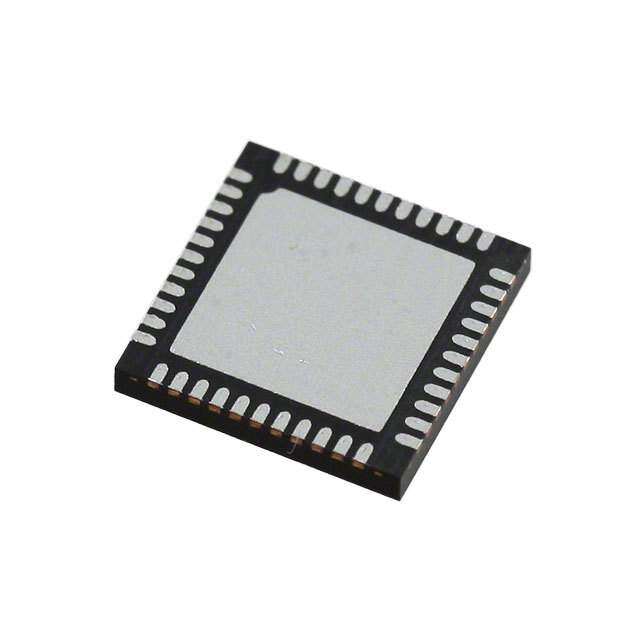
| 描述 | IC CLOCK DUAL PLL 64WQFN时钟合成器/抖动清除器 Lo-Noise Clock Jittr Cleaner Dual Lp PLL |
| 产品分类 | |
| 品牌 | Texas Instruments |
| 产品手册 | |
| 产品图片 |
|
| rohs | 符合RoHS无铅 / 符合限制有害物质指令(RoHS)规范要求 |
| 产品系列 | 时钟和计时器IC,时钟合成器/抖动清除器,Texas Instruments LMK04808BISQE/NOPBPLLatinum™ |
| 数据手册 | |
| 产品型号 | LMK04808BISQE/NOPB |
| PCN组件/产地 | |
| PLL | 是 |
| 产品种类 | 时钟合成器/抖动清除器 |
| 供应商器件封装 | 64-WQFN (9x9) |
| 其它名称 | *LMK04808BISQE/NOPB |
| 分频器/倍频器 | 是/无 |
| 包装 | 剪切带 (CT) |
| 商标 | Texas Instruments |
| 安装类型 | 表面贴装 |
| 安装风格 | SMD/SMT |
| 封装 | Reel |
| 封装/外壳 | 64-WFQFN 裸露焊盘 |
| 封装/箱体 | WQFN-64 |
| 工作温度 | -40°C ~ 85°C |
| 工厂包装数量 | 250 |
| 差分-输入:输出 | 是/是 |
| 最大工作温度 | + 85 C |
| 最大输出频率 | 3072 MHz |
| 最小工作温度 | - 40 C |
| 标准包装 | 1 |
| 比率-输入:输出 | 2:14 |
| 特色产品 | http://www.digikey.com/cn/zh/ph/ns/lmk04800-clock-conditioner.html |
| 电压-电源 | 3.15 V ~ 3.45 V |
| 电源电压-最大 | 3.45 V |
| 电源电压-最小 | 3.15 V |
| 电源电流 | 505 mA |
| 电路数 | 1 |
| 类型 | 抖动消除器 |
| 系列 | LMK04800 |
| 输入 | LVCMOS,LVDS,LVPECL |
| 输入电平 | LVPECL, LVDS, LVCMOS |
| 输出 | LVCMOS,LVDS,LVPECL |
| 输出电平 | LVCMOS, LVPECL, LVDS |
| 输出端数量 | 12 |
| 频率-最大值 | 1.536GHz |


PDF Datasheet 数据手册内容提取
Product Sample & Technical Tools & Support & Folder Buy Documents Software Community LMK04803,LMK04805,LMK04806,LMK04808 SNAS489K–MARCH2011–REVISEDDECEMBER2014 LMK0480x Low-Noise Clock Jitter Cleaner with Dual Loop PLLs 1 Features 3 Description • Ultra-LowRMSJitterPerformance The LMK0480x family is the industry's highest 1 performance clock conditioner with superior clock – 111fsRMSJitter(12kHzto20MHz) jitter cleaning, generation, and distribution with – 123fsRMSJitter(100Hzto20MHz) advanced features to meet next generation system • DualLoopPLLatinum™PLLArchitecture requirements. The dual loop PLLatinum™ architecture is capable of 111 fs rms jitter (12 kHz to • PLL1 20 MHz) using a low noise VCXO module or sub-200 – IntegratedLow-NoiseCrystalOscillatorCircuit fs rms jitter (12 kHz to 20 MHz) using a low cost – HoldoverModewhenInputClocksareLost externalcrystalandvaractordiode. – AutomaticorManualTriggering/Recovery The dual loop architecture consists of two high- • PLL2 performance phase-locked loops (PLL), a low-noise crystal oscillator circuit, and a high-performance – NormalizedPLLNoiseFloorof–227dBc/Hz voltage controlled oscillator (VCO). The first PLL – PhaseDetectorRateupto155MHz (PLL1) provides low-noise jitter cleaner functionality – OSCinFrequency-Doubler while the second PLL (PLL2) performs the clock generation. PLL1 can be configured to either work – IntegratedLow-NoiseVCO with an external VCXO module or the integrated • 2RedundantInputClockswithLOS crystal oscillator with an external tunable crystal and – AutomaticandManualSwitch-OverModes varactor diode. When paired with a very narrow loop bandwidth, PLL1 uses the superior close-in phase • 50%DutyCycleOutputDivides,1to1045(Even noise (offsets below 50 kHz) of the VCXO module or andOdd) the tunable crystal to clean the input clock. The • 12LVPECL,LVDS,orLVCMOSProgrammable outputofPLL1isusedasthecleaninputreferenceto Outputs PLL2 where it locks the integrated VCO. The loop • DigitalDelay:FixedorDynamicallyAdjustable bandwidth of PLL2 can be optimized to clean the far- out phase noise (offsets above 50 kHz) where the • 25psStepAnalogDelayControl. integrated VCO outperforms the VCXO module or • 14DifferentialOutputs.Upto26SingleEnded. tunablecrystalusedinPLL1. – Upto6VCXO/CrystalBufferedOutputs • ClockRatesofupto1536MHz DeviceInformation • 0-DelayMode PARTNUMBER VCOFREQUENCY REFERENCE INPUTS • ThreeDefaultClockOutputsatPowerUp LMK04803 1840to2030MHz • Multi-Mode:DualPLL,SinglePLL,andClock LMK04805 2148to2370MHz Distribution 2 LMK04806 2370to2600MHz • IndustrialTemperatureRange:–40to85°C LMK04808 2750to3072MHz • 3.15-Vto3.45-VOperation (1) For all available packages, see the orderable addendum at • 2DedicatedBuffered/DividedOSCinClocks theendofthedatasheet. • Package:64-PinWQFN(9.0× 9.0 ×0.8mm) SimplifiedSchematic 2 Applications OSCout0/ Recovered CVryCsXtaOl or OSCout1 LMX2541 0cloXcOWkLSsO Ha(cid:3)t³ FdOiHffDeQre´(cid:3)nt • DataConverterClocking ³GLUW\´(cid:3)FORFN(cid:3)RU(cid:3) PLL+VCO frequencies clean clock CLKin0 CLKout0, 1 • WirelessInfrastructure Backup LMK0480x CLKout2 • Networking,SONET/SDH,DSLAM RCelofcekrence CLKin1 Precision Clock CLKout3 FFPPGGAA DSeesreiarilaizliezre/r Conditioner • Medical/Video/Military/Aerospace I CLKout4, 5, 6, 7 • TestandMeasurement CLKout11 CLKout8A IF CLKout9 ADC DDAACC CPLD Q 1 An IMPORTANT NOTICE at the end of this data sheet addresses availability, warranty, changes, use in safety-critical applications, intellectualpropertymattersandotherimportantdisclaimers.PRODUCTIONDATA.
LMK04803,LMK04805,LMK04806,LMK04808 SNAS489K–MARCH2011–REVISEDDECEMBER2014 www.ti.com Table of Contents 1 Features.................................................................. 1 8.5 Programming...........................................................47 2 Applications........................................................... 1 8.6 RegisterMaps.........................................................51 3 Description............................................................. 1 9 ApplicationandImplementation........................ 97 4 RevisionHistory..................................................... 2 9.1 ApplicationInformation............................................97 9.2 TypicalApplications..............................................114 5 PinConfigurationandFunctions......................... 4 9.3 SystemExamples.................................................122 6 Specifications......................................................... 6 9.4 Do'sandDon'ts.....................................................124 6.1 AbsoluteMaximumRatings......................................6 10 PowerSupplyRecommendations................... 125 6.2 ESDRatings..............................................................6 10.1 PinConnectionRecommendations.....................125 6.3 RecommendedOperatingConditions.......................6 10.2 CurrentConsumptionandPowerDissipation 6.4 ThermalInformation..................................................7 Calculations............................................................126 6.5 ElectricalCharacteristics...........................................7 11 Layout................................................................. 129 6.6 TimingRequirements..............................................13 11.1 LayoutGuidelines...............................................129 6.7 TypicalCharacteristics:ClockOutputAC Characteristics.........................................................14 11.2 LayoutExample..................................................130 7 ParameterMeasurementInformation................15 12 DeviceandDocumentationSupport............... 131 7.1 ChargePumpCurrentSpecificationDefinitions......15 12.1 DeviceSupport....................................................131 7.2 DifferentialVoltageMeasurementTerminology......16 12.2 DocumentationSupport......................................131 12.3 RelatedLinks......................................................131 8 DetailedDescription............................................ 17 12.4 Trademarks.........................................................131 8.1 Overview.................................................................17 12.5 ElectrostaticDischargeCaution..........................131 8.2 FunctionalBlockDiagram.......................................21 12.6 Glossary..............................................................131 8.3 FeatureDescription.................................................22 13 Mechanical,Packaging,andOrderable 8.4 DeviceFunctionalModes........................................43 Information......................................................... 131 4 Revision History ChangesfromRevisionJ(March2013)toRevisionK Page • Changed90to80and80to90forf parameterinElectricalCharacteristics....................................................... 11 CLKout-startup • Added"SpecificationisnotvalidforCLKoutXorCLKoutYinanalogdelaymode"intablenoteforElectrical Characteristics ..................................................................................................................................................................... 11 • Changed"Temperature"to"AmbientTemperature"inheadingtitled"ChargePumpOutputCurrentMagnitude Variationvs.AmbientTemperature" .................................................................................................................................... 15 • Added"temporarily"inVCXO/CRYSTALBufferedOutputs ................................................................................................ 18 • Changedfrom"npossible"to"Dpossible"in0-Delay......................................................................................................... 20 • Changed"can"to"cannot"inInputClockSwitching-PinSelectMode.............................................................................. 24 • DeletedClockSwitchEventwithoutHoldoverinClockSwitchEventwithHoldover.......................................................... 25 • Addedparagraphbeginning"Forapplications..."inPLL2FrequencyDoubler................................................................... 29 • Changed5to15inTable11................................................................................................................................................. 42 • DeletedMode5rowinTable12.......................................................................................................................................... 43 • AddedMode15AdditionalConfigurationssection.............................................................................................................. 46 • InTable16,added[27:26],[23:22],and[21:20]forRegister27row.Added[31:20]forR28.Added[26:24]forR30. Added[7:6]........................................................................................................................................................................... 51 • InTable18,changed"ActualPLL2Ndividervalueusedincalibrationroutine".Addedfootnote"InversionforStatus 0and1pinsisonlyvalidforCLKin_SELECT_MODE=0x06"............................................................................................ 56 • InTable28,added"toreducesupply..."footnotefor9through14.Addedfootnote"Toreducesupplyswitchingand crosstalknoise,itisrecommendedtouseacomplementaryLVCMOSoutputtypesuchas6or7".................................. 64 • Addedfootnote"Toreducesupply"for8through14inTable32 ....................................................................................... 66 • Changed"Divide"to"Definition"inTable39,Table40,Table61,andTable62................................................................ 68 • Changedto"MUXOUTPUT"inTableheaderrowinTable42............................................................................................ 69 • InTable43,addedfootnote,"ContactTIApplicationsformoreinformationonusingthismode".Changedto"Dual 2 SubmitDocumentationFeedback Copyright©2011–2014,TexasInstrumentsIncorporated ProductFolderLinks:LMK04803 LMK04805 LMK04806 LMK04808
LMK04803,LMK04805,LMK04806,LMK04808 www.ti.com SNAS489K–MARCH2011–REVISEDDECEMBER2014 Revision History (continued) PLL,ExternalVCO(Fin),0-Delay"for15(0x0F)................................................................................................................. 70 • Added"InversionforStatus0and1pinsisonlyvalidforCLKin_SELECT_MODE=0x06"inCLKin_Sel_INV.................78 • InFORCE_HOLDOVER,added"(EN_TRACK=0or1,EN_MAN_DAC=1)".Added"(EN_TRACK=1, EN_MAN_DAC=0,EN_VTUNE_RAIL_DET=0)".............................................................................................................. 82 • ChangedtoR[23:14]inDAC_CNT....................................................................................................................................... 83 • InTable90,added(0x0000),(0x0001),(0x0002),(0x0003).Changed"Divide"to"Value"intheheaderrow................... 87 • Added(0x00)through(0x04)inTable91............................................................................................................................. 88 • AddedPLL2FrequencyDoubler.......................................................................................................................................... 88 • Changedfrom"Divide"to"Value"inTable95..................................................................................................................... 89 • AddedPLL2FrequencyDoublerreferenceinTable103..................................................................................................... 92 • Addednote"Unlessin0-delay..."inPLL2_N_CAL,PLL2NCalibrationDivider ................................................................ 93 • Changed"Mode_MUX1"to"VCO_MUX"inPLL2_P,PLL2NPrescalerDivider................................................................. 94 • Changed"register"to"Defintion"intableheaderrowforTable110................................................................................... 95 • UpdatedMinimumDigitalLockDetectTimeCalculationExample ................................................................................... 107 • Added"PerformanceofotherLMK0480xdeviceswillbesimilar"inOptionalCrystalOscillatorImplementation (OSCin/OSCin*).................................................................................................................................................................. 110 • Changedto"(fsrms)"inTable125 ................................................................................................................................... 111 • AddedtextinredforFigure40 .......................................................................................................................................... 123 • InVcc2,Vcc3,Vcc10,Vcc11,Vcc12,Vcc13(CLKoutVccs),addedbulletpointstartingwith"Itisrecommended..." Changed≤10MHzto≤30MHz........................................................................................................................................ 125 • Addedparagraph"Itisrecommended..."inVcc5(CLKinandOSCout1),Vcc7(OSCinandOSCout0)........................... 126 • AddedMode=15.RemovedMode=5inTable127........................................................................................................ 127 • Deleted"ofabout2squareinches"inLayoutGuidelines.................................................................................................. 129 ChangesfromRevisionI(March2013)toRevisionJ Page • ChangedlayoutofNationalDataSheettoTIformat............................................................................................................. 1 Copyright©2011–2014,TexasInstrumentsIncorporated SubmitDocumentationFeedback 3 ProductFolderLinks:LMK04803 LMK04805 LMK04806 LMK04808
LMK04803,LMK04805,LMK04806,LMK04808 SNAS489K–MARCH2011–REVISEDDECEMBER2014 www.ti.com 5 Pin Configuration and Functions 64-PinWQFNwithExposedPad NKDPackage (TopView) 1 0 n n Vcc13 Status_CLKi Status_CLKi CLKout11 CLKout11* CLKout10* CLKout10 Vcc12 CLKout9 CLKout9* CLKout8* CLKout8 Vcc11 CLKout7 CLKout7* CLKout6* 64 63 62 61 60 59 58 57 56 55 54 53 52 51 50 49 CLKout0 1 48 CLKout6 CLKout0* 2 47 Vcc10 CLKout1* 3 46 DATAuWire CLKout1 4 45 CLKuWire NC 5 44 LEuWire SYNC 6 43 Vcc9 NC 7 42 CPout2 NC 8 41 Vcc8 Top Down View NC 9 40 OSCout0* Vcc1 10 39 OSCout0 LDObyp1 11 38 Vcc7 LDObyp2 12 37 OSCin* CLKout2 13 36 OSCin CLKout2* 14 35 Vcc6 CLKout3* 15 DAP 34 CPout1 CLKout3 16 33 Status_LD 17 18 19 20 21 22 23 24 25 26 27 28 29 30 31 32 Vcc2 Vcc3 CLKout4 CLKout4* CLKout5* CLKout5 GND Vcc4 CLKin/Fin/CLKin1 Kin*/Fin*/CLKin1* Status_Holdover CLKin0 CLKin0* Vcc5 OSCout1 OSCout1* FB BCL F PinFunctions(1) PIN I/O TYPE DESCRIPTION NUMBER NAME 1,2 CLKout0,CLKout0* O Programmable Clockoutput0(clockgroup0). 3,4 CLKout1*,CLKout1 O Programmable Clockoutput1(clockgroup0). 6 SYNC I/O Programmable CLKoutSynchronizationinputorprogrammablestatuspin. 5,7,8,9 NC – – NoConnection.Thesepinsmustbeleftfloating. 10 Vcc1 PWR PowersupplyforVCOLDO. 11 LDObyp1 ANLG LDOBypass,bypassedtogroundwith10µFcapacitor. 12 LDObyp2 ANLG LDOBypass,bypassedtogroundwitha0.1µFcapacitor. 13,14 CLKout2,CLKout2* O Programmable Clockoutput2(clockgroup1). 15,16 CLKout3*,CLKout3 O Programmable Clockoutput3(clockgroup1). 17 Vcc2 PWR Powersupplyforclockgroup1:CLKout2andCLKout3. 18 Vcc3 PWR Powersupplyforclockgroup2:CLKout4andCLKout5. (1) SeePinConnectionRecommendations. 4 SubmitDocumentationFeedback Copyright©2011–2014,TexasInstrumentsIncorporated ProductFolderLinks:LMK04803 LMK04805 LMK04806 LMK04808
LMK04803,LMK04805,LMK04806,LMK04808 www.ti.com SNAS489K–MARCH2011–REVISEDDECEMBER2014 PinFunctions(1)(continued) PIN I/O TYPE DESCRIPTION NUMBER NAME 19,20 CLKout4,CLKout4* O Programmable Clockoutput4(clockgroup2). 21,22 CLKout5*,CLKout5 O Programmable Clockoutput5(clockgroup2). 23 GND PWR Ground. 24 Vcc4 PWR Powersupplyfordigital. CLKin1,CLKin1* ReferenceClockInputPort1forPLL1.ACorDCCoupled. Feedbackinputforexternalclockfeedbackinput(0-delay FBCLKin,FBCLKin* 25,26 I ANLG mode).ACorDCCoupled. ExternalVCOinput(ExternalVCOmode).ACorDC Fin/Fin* Coupled. Programmablestatuspin,defaultreadbackoutput. 27 Status_Holdover I/O Programmable Programmabletoholdovermodeindicator.Otheroptions availablebyprogramming. ReferenceClockInputPort0forPLL1. 28,29 CLKin0,CLKin0* I ANLG ACorDCCoupled. 30 Vcc5 PWR PowersupplyforclockinputsandOSCout1. 31,32 OSCout1,OSCout1* O LVPECL Bufferedoutput1ofOSCinport. Programmablestatuspin,defaultlockdetectforPLL1and 33 Status_LD I/O Programmable PLL2.Otheroptionsavailablebyprogramming. 34 CPout1 O ANLG Chargepump1output. 35 Vcc6 PWR PowersupplyforPLL1,chargepump1. FeedbacktoPLL1,ReferenceinputtoPLL2. 36,37 OSCin,OSCin* I ANLG ACCoupled. 38 Vcc7 PWR PowersupplyforOSCin,OSCout0,andPLL2circuitry.(2) 39,40 OSCout0,OSCout0* O Programmable Bufferedoutput0ofOSCinport.(2) 41 Vcc8 PWR PowersupplyforPLL2,chargepump2. 42 CPout2 O ANLG Chargepump2output. 43 Vcc9 PWR PowersupplyforPLL2. 44 LEuWire I CMOS MICROWIRELatchEnableInput. 45 CLKuWire I CMOS MICROWIREClockInput. 46 DATAuWire I CMOS MICROWIREDataInput. 47 Vcc10 PWR Powersupplyforclockgroup3:CLKout6andCLKout7. 48,49 CLKout6,CLKout6* O Programmable Clockoutput6(clockgroup3). 50,51 CLKout7*,CLKout7 O Programmable Clockoutput7(clockgroup3). 52 Vcc11 PWR Powersupplyforclockgroup4:CLKout8andCLKout9. 53,54 CLKout8,CLKout8* O Programmable Clockoutput8(clockgroup4). 55,56 CLKout9*,CLKout9 O Programmable Clockoutput9(clockgroup4). 57 Vcc12 PWR Powersupplyforclockgroup5:CLKout10andCLKout11. CLKout10, 58,59 O Programmable Clockoutput10(clockgroup5). CLKout10* CLKout11*, 60,61 O Programmable Clockoutput11(clockgroup5). CLKout11 Programmablestatuspin.Defaultisinputforpincontrolof 62 Status_CLKin0 I/O Programmable PLL1referenceclockselection.CLKin0LOSstatusand otheroptionsavailablebyprogramming. Programmablestatuspin.Defaultisinputforpincontrolof 63 Status_CLKin1 I/O Programmable PLL1referenceclockselection.CLKin1LOSstatusand otheroptionsavailablebyprogramming. 64 Vcc13 PWR Powersupplyforclockgroup0:CLKout0andCLKout1. DAP DAP – GND DIEATTACHPAD,connecttoGND. (2) SeeVcc5(CLKinandOSCout1),Vcc7(OSCinandOSCout0)forinformationonconfiguringdeviceforoptimumperformance. Copyright©2011–2014,TexasInstrumentsIncorporated SubmitDocumentationFeedback 5 ProductFolderLinks:LMK04803 LMK04805 LMK04806 LMK04808
LMK04803,LMK04805,LMK04806,LMK04808 SNAS489K–MARCH2011–REVISEDDECEMBER2014 www.ti.com 6 Specifications 6.1 Absolute Maximum Ratings(1)(2)(3) overoperatingfree-airtemperaturerange(unlessotherwisenoted) (4) MIN MAX UNIT V SupplyVoltage (5) –0.3 3.6 V CC (V + V InputVoltage –0.3 CC V IN 0.3) T LeadTemperature(solder4seconds) +260 °C L T JunctionTemperature 150 °C J DifferentialInputCurrent(CLKinX/X*, I ±5 mA IN OSCin/OSCin*,FBCLKin/FBCLKin*,Fin/Fin*) MSL MoistureSensitivityLevel 3 T Storagetemperaturerange -65 150 °C stg (1) "AbsoluteMaximumRatings"indicatelimitsbeyondwhichdamagetothedevicemayoccur.OperatingRatingsindicateconditionsfor whichthedeviceisintendedtobefunctional,butdonotensurespecificperformancelimits.Forensuredspecificationsandtest conditions,seetheElectricalCharacteristics.Theensuredspecificationsapplyonlytothetestconditionslisted. (2) Stressesinexcessoftheabsolutemaximumratingscancausepermanentorlatentdamagetothedevice.Theseareabsolutestress ratingsonly.Functionaloperationofthedeviceisonlyimpliedattheseoranyotherconditionsinexcessofthosegivenintheoperation sectionsofthedatasheet.Exposuretoabsolutemaximumratingsforextendedperiodscanadverselyaffectdevicereliability. (3) IfMilitary/Aerospacespecifieddevicesarerequired,contacttheTexasInstrumentsSalesOffice/Distributorsforavailabilityand specifications. (4) StressesbeyondthoselistedunderAbsoluteMaximumRatingsmaycausepermanentdamagetothedevice.Thesearestressratings only,whichdonotimplyfunctionaloperationofthedeviceattheseoranyotherconditionsbeyondthoseindicatedunderRecommended OperatingConditions.Exposuretoabsolute-maximum-ratedconditionsforextendedperiodsmayaffectdevicereliability. (5) Nevertoexceed3.6V. 6.2 ESD Ratings VALUE UNIT Human-bodymodel(HBM),perANSI/ESDA/JEDECJS-001(1) ±2000 Machinemodel(MM) ±150 V Electrostaticdischarge V (ESD) Charged-devicemodel(CDM),perJEDECspecificationJESD22- C101(2) ±750 (1) JEDECdocumentJEP155statesthat500-VHBMallowssafemanufacturingwithastandardESDcontrolprocess.Manufacturingwith lessthan500-VHBMispossiblewiththenecessaryprecautions.Pinslistedas±2000Vmayactuallyhavehigherperformance. (2) JEDECdocumentJEP157statesthat250-VCDMallowssafemanufacturingwithastandardESDcontrolprocess.Manufacturingwith lessthan250-VCDMispossiblewiththenecessaryprecautions.Pinslistedas±750Vmayactuallyhavehigherperformance. 6.3 Recommended Operating Conditions MIN NOM MAX UNIT T JunctionTemperature 125 °C J T AmbientTemperature V =3.3V -40 25 85 °C A CC V SupplyVoltage 3.15 3.3 3.45 V CC 6 SubmitDocumentationFeedback Copyright©2011–2014,TexasInstrumentsIncorporated ProductFolderLinks:LMK04803 LMK04805 LMK04806 LMK04808
LMK04803,LMK04805,LMK04806,LMK04808 www.ti.com SNAS489K–MARCH2011–REVISEDDECEMBER2014 6.4 Thermal Information LMK0480x THERMALMETRIC(1) NKD UNIT 64PINS R Junction-to-ambientthermalresistanceon4-layerJEDECPCB(2)(3) 25.2 θJA R Junction-to-case(top)thermalresistance(4)(5) 6.9 θJC(top) R Junction-to-boardthermalresistance(6) 4.0 θJB °C/W ψ Junction-to-topcharacterizationparameter(7) 0.1 JT ψ Junction-to-boardcharacterizationparameter(8) 4.0 JB R Junction-to-case(bottom)thermalresistance(9) 0.8 θJC(bot) (1) Formoreinformationabouttraditionalandnewthermalmetrics,seetheICPackageThermalMetricsapplicationreport,SPRA953. (2) Thejunction-to-ambientthermalresistanceundernaturalconvectionisobtainedinasimulationonaJEDEC-standard,High-Kboard,as specifiedinJESD51-7,inanenvironmentdescribedinJESD51-2a. (3) Specificationassumes32thermalviasconnectthedieattachpadtotheembeddedcopperplaneonthe4-layerJEDECPCB.These viasplayakeyroleinimprovingthethermalperformanceoftheWQFN.NotethattheJEDECPCBisastandardthermalmeasurement PCBanddoesnotrepresentbestperformanceaPCBcanachieve.Itisrecommendedthatthemaximumnumberofviasbeusedinthe boardlayout.R isuniqueforeachPCB. θJA (4) Thejunction-to-case(top)thermalresistanceisobtainedbysimulatingacoldplatetestonthepackagetop.NospecificJEDECstandard testexists,butaclosedescriptioncanbefoundintheANSISEMIstandardG30-88. (5) CaseisdefinedastheDAP(dieattachpad) (6) Thejunction-to-boardthermalresistanceisobtainedbysimulatinganenvironmentwitharingcoldplatefixturetocontrolthePCB temperature,asdescribedinJESD51-8. (7) Thejunction-to-topcharacterizationparameter,ψ ,estimatesthejunctiontemperatureofadeviceinarealsystemandisextracted JT fromthesimulationdataforobtainingR ,usingaproceduredescribedinJESD51-2a(sections6and7). θJA (8) Thejunction-to-boardcharacterizationparameter,ψ ,estimatesthejunctiontemperatureofadeviceinarealsystemandisextracted JB fromthesimulationdataforobtainingR ,usingaproceduredescribedinJESD51-2a(sections6and7). θJA (9) Thejunction-to-case(bottom)thermalresistanceisobtainedbysimulatingacoldplatetestontheexposed(power)pad.Nospecific JEDECstandardtestexists,butaclosedescriptioncanbefoundintheANSISEMIstandardG30-88. 6.5 Electrical Characteristics 3.15V≤V ≤3.45V,-40°C≤T ≤85°C.TypicalvaluesrepresentmostlikelyparametricnormsatV =3.3V,T =25°C, CC A CC A attheRecommendedOperatingConditionsatthetimeofproductcharacterizationandarenotspecified.(1) PARAMETER TESTCONDITIONS MIN TYP MAX UNIT CURRENTCONSUMPTION NoDCpathtogroundon ICC_PD Powerdownsupplycurrent OSCout1/1*(2) 1 3 mA Allclockdelaysdisabled, I Supplycurrentwithallclocksenabled(3) CLKoutX_Y_DIV=1045, 505 590 mA CC_CLKS CLKoutX_TYPE=1(LVDS), PLL1andPLL2locked. CLKin0/0*andCLKin1/1*INPUTCLOCKSPECIFICATIONS f Clockinputfrequency(4) 0.001 500 MHz CLKin SLEW (1) Clockinputslewrate(5) 20%to80% 0.15 0.5 V/ns CLKin VIDCLKin ACcoupled 0.25 1.55 |V| V CLKin Clockinput CLKinX_BUF_TYPE=0(Bipolar) 0.5 3.1 Vpp SS Differentialinputvoltage(see (6)and VIDCLKin Figure4) ACcoupled 0.25 1.55 |V| V CLKin CLKinX_BUF_TYPE=1(MOS) 0.5 3.1 Vpp SS (1) Inordertomeetthejitterperformancelistedinthesubsequentsectionsofthisdatasheet,theminimumrecommendedslewrateforall inputclocksis0.5V/ns.Thisisespeciallytrueforsingle-endedclocks.Phasenoiseperformancewillbegintodegradeastheclockinput slewrateisreduced.However,thedevicewillfunctionatslewratesdowntotheminimumlisted.Whencomparedtosingle-ended clocks,differentialclocks(LVDS,LVPECL)willbelesssusceptibletodegradationinphasenoiseperformanceatlowerslewratesdueto theircommonmodenoiserejection.However,itisalsorecommendedtousethehighestpossibleslewratefordifferentialclocksto achieveoptimalphasenoiseperformanceatthedeviceoutputs. (2) IfemitterresistorsareplacedontheOSCout1/1*pins,therewillbeaDCcurrenttogroundwhichwillcausepowerdownIcctoincrease. (3) Loadconditionsforoutputclocks:LVDS:100-Ωdifferential.SeeCurrentConsumptionandPowerDissipationCalculationsforIccfor specificpartconfigurationandhowtocalculateIccforaspecificdesign. (4) CLKin0,CLKin1maximumisspecifiedbycharacterization,productiontestedat200MHz. (5) Specifiedbycharacterization. (6) SeeDifferentialVoltageMeasurementTerminologyfordefinitionofV andV voltages. ID OD Copyright©2011–2014,TexasInstrumentsIncorporated SubmitDocumentationFeedback 7 ProductFolderLinks:LMK04803 LMK04805 LMK04806 LMK04808
LMK04803,LMK04805,LMK04806,LMK04808 SNAS489K–MARCH2011–REVISEDDECEMBER2014 www.ti.com Electrical Characteristics (continued) 3.15V≤V ≤3.45V,-40°C≤T ≤85°C.TypicalvaluesrepresentmostlikelyparametricnormsatV =3.3V,T =25°C, CC A CC A attheRecommendedOperatingConditionsatthetimeofproductcharacterizationandarenotspecified.(1) PARAMETER TESTCONDITIONS MIN TYP MAX UNIT ACcoupledtoCLKinX;CLKinX*AC coupledtoGround 0.25 2.4 Vpp Clockinput CLKinX_BUF_TYPE=0(Bipolar) VCLKin Single-endedinputvoltage(5) ACcoupledtoCLKinX;CLKinX*AC coupledtoGround 0.25 2.4 Vpp CLKinX_BUF_TYPE=1(MOS) DCoffsetvoltagebetween V CLKin0/CLKin0* 20 mV CLKin0-offset CLKin0*-CLKin0 EachpinACcoupled DCoffsetvoltagebetween CLKin0_BUF_TYPE=0(Bipolar) V CLKin1/CLKin1* 0 mV CLKin1-offset CLKin1*-CLKin1 DCoffsetvoltagebetween EachpinACcoupled V CLKinX/CLKinX* 55 mV CLKinX-offset CLKinX_BUF_TYPE=1(MOS) CLKinX*-CLKinX V V Highinputvoltage DCcoupledtoCLKinX;CLKinX*AC 2.0 V V CLKin- IH CC coupledtoGround VCLKin-VIL Lowinputvoltage CLKinX_BUF_TYPE=1(MOS) 0.0 0.4 V FBCLKin/FBCLKin*andFin/Fin*INPUTSPECIFICATIONS ACcoupled f Clockinputfrequency(5) (CLKinX_BUF_TYPE=0) 0.001 1000 MHz FBCLKin MODE=2or8;FEEDBACK_MUX= 6 ACcoupled f Clockinputfrequency(5) (CLKinX_BUF_TYPE=0) 0.001 3100 MHz Fin MODE=3or11 SingleEnded ACcoupled; VFBCLKin/Fin Clockinputvoltage(5) (CLKinX_BUF_TYPE=0) 0.25 2.0 Vpp SLEW SlewrateonCLKin(5) ACcoupled;20%to80%; 0.15 0.5 V/ns FBCLKin/Fin (CLKinX_BUF_TYPE=0) PLL1SPECIFICATIONS f PLL1phasedetectorfrequency 40 MHz PD1 V =V /2,PLL1_CP_GAIN=0 100 CPout1 CC PLL1charge VCPout1=VCC/2,PLL1_CP_GAIN=1 200 ICPout1SOURCE Pumpsourcecurrent(7) V =V /2,PLL1_CP_GAIN=2 400 µA CPout1 CC V =V /2,PLL1_CP_GAIN=3 1600 CPout1 CC V =V /2,PLL1_CP_GAIN=0 -100 CPout1 CC PLL1charge VCPout1=VCC/2,PLL1_CP_GAIN=1 -200 ICPout1SINK Pumpsinkcurrent(7) V =V /2,PLL1_CP_GAIN=2 -400 µA CPout1 CC V =V /2,PLL1_CP_GAIN=3 -1600 CPout1 CC Chargepump I %MIS V =V /2,T=25°C 3% 10% CPout1 Sink/sourcemismatch CPout1 CC Magnitudeofchargepumpcurrent 0.5V<V <V -0.5V I V CPout1 CC 4% CPout1 TUNE variationvs.chargepumpvoltage T =25°C A Chargepumpcurrentvs. I %TEMP 4% CPout1 temperaturevariation ChargePumpTRI-STATEleakage I TRI 0.5V<V <V -0.5V 5 nA CPout1 current CPout CC (7) Thisparameterisprogrammable 8 SubmitDocumentationFeedback Copyright©2011–2014,TexasInstrumentsIncorporated ProductFolderLinks:LMK04803 LMK04805 LMK04806 LMK04808
LMK04803,LMK04805,LMK04806,LMK04808 www.ti.com SNAS489K–MARCH2011–REVISEDDECEMBER2014 Electrical Characteristics (continued) 3.15V≤V ≤3.45V,-40°C≤T ≤85°C.TypicalvaluesrepresentmostlikelyparametricnormsatV =3.3V,T =25°C, CC A CC A attheRecommendedOperatingConditionsatthetimeofproductcharacterizationandarenotspecified.(1) PARAMETER TESTCONDITIONS MIN TYP MAX UNIT PLL1/fnoiseat10kHzoffset.(8) PLL1_CP_GAIN=400µA -117 PN10kHz dBc/Hz Normalizedto1GHzOutputFrequency PLL1_CP_GAIN=1600µA -118 PLL1_CP_GAIN=400µA -221.5 PN1Hz Normalizedphasenoisecontribution(9) dBc/Hz PLL1_CP_GAIN=1600µA -223 PLL2REFERENCEINPUT(OSCin)SPECIFICATIONS f PLL2referenceinput(10) 500 MHz OSCin PLL2referenceclockminimumslewrate SLEWOSCin onOSCin(5) 20%to80% 0.15 0.5 V/ns V InputvoltageforOSCinorOSCin*(5) ACcoupled;Single-ended(Unused 0.2 2.4 Vpp OSCin pinACcoupledtoGND) V OSCin 0.2 1.55 |V| ID Differentialvoltageswing(seeFigure4) ACcoupled V OSCin 0.4 3.1 Vpp SS DCoffsetvoltagebetween V OSCin/OSCin* EachpinACcoupled 20 mV OSCin-offset OSCinX*-OSCinX f Doublerinputfrequency(5) EN_PLL2_REF_2X=1;(11) 155 MHz doubler_max OSCinDutyCycle40%to60% CRYSTALOSCILLATORMODESPECIFICATIONS f Crystalfrequencyrange(5) R <40Ω 6 20.5 MHz XTAL ESR VectronVXB1crystal,20.48MHz, P Crystalpowerdissipation(12) R <40Ω 100 µW XTAL ESR XTAL_LVL=0 Inputcapacitanceof C -40to+85°C 6 pF IN LMK0480xOSCinport PLL2PHASEDETECTORandCHARGEPUMPSPECIFICATIONS f Phasedetectorfrequency 155 MHz PD2 V =V /2,PLL2_CP_GAIN=0 100 CPout2 CC V =V /2,PLL2_CP_GAIN=1 400 I SOURCE PLL2chargepumpsourcecurrent(7) CPout2 CC µA CPout V =V /2,PLL2_CP_GAIN=2 1600 CPout2 CC V =V /2,PLL2_CP_GAIN=3 3200 CPout2 CC V =V /2,PLL2_CP_GAIN=0 -100 CPout2 CC V =V /2,PLL2_CP_GAIN=1 -400 I SINK PLL2chargepumpsinkcurrent(7) CPout2 CC µA CPout V =V /2,PLL2_CP_GAIN=2 -1600 CPout2 CC V =V /2,PLL2_CP_GAIN=3 -3200 CPout2 CC I %MIS Chargepumpsink/sourcemismatch V =V /2,T =25°C 3% 10% CPout2 CPout2 CC A Magnitudeofchargepumpcurrentvs. 0.5V<V <V -0.5V I V CPout2 CC 4% CPout2 TUNE chargepumpvoltagevariation T =25°C A (8) AspecificationinmodelingPLLin-bandphasenoiseisthe1/fflickernoise,L (f),whichisdominantclosetothecarrier.Flicker PLL_flicker noisehasa10dB/decadeslope.PN10kHzisnormalizedtoa10kHzoffsetanda1GHzcarrierfrequency.PN10kHz=L (10 PLL_flicker kHz)-20log(Fout/1GHz),whereL (f)isthesinglesidebandphasenoiseofonlytheflickernoise'scontributiontototalnoise, PLL_flicker L(f).TomeasureL (f)itisimportanttobeonthe10dB/decadeslopeclosetothecarrier.Ahighcomparefrequencyandaclean PLL_flicker crystalareimportanttoisolatingthisnoisesourcefromthetotalphasenoise,L(f).L (f)canbemaskedbythereference PLL_flicker oscillatorperformanceifalowpowerornoisysourceisused.ThetotalPLLin-bandphasenoiseperformanceisthesumofL (f) PLL_flicker andL (f). PLL_flat (9) AspecificationmodelingPLLin-bandphasenoise.ThenormalizedphasenoisecontributionofthePLL,L (f),isdefinedas: PLL_flat PN1HZ=L (f)-20log(N)-10log(f ).L (f)isthesinglesidebandphasenoisemeasuredatanoffsetfrequency,f,ina1Hz PLL_flat PDX PLL_flat bandwidthandf isthephasedetectorfrequencyofthesynthesizer.L (f)contributestothetotalnoise,L(f). PDX PLL_flat (10) F maximumfrequencyspecifiedbycharacterization.Productiontestedat200MHz. OSCin (11) TheEN_PLL2_REF_2Xbit(Register13)enables/disablesafrequencydoublermodeforthePLL2OSCinpath. (12) SeeApplicationSectiondiscussionofOptionalCrystalOscillatorImplementation(OSCin/OSCin*). Copyright©2011–2014,TexasInstrumentsIncorporated SubmitDocumentationFeedback 9 ProductFolderLinks:LMK04803 LMK04805 LMK04806 LMK04808
LMK04803,LMK04805,LMK04806,LMK04808 SNAS489K–MARCH2011–REVISEDDECEMBER2014 www.ti.com Electrical Characteristics (continued) 3.15V≤V ≤3.45V,-40°C≤T ≤85°C.TypicalvaluesrepresentmostlikelyparametricnormsatV =3.3V,T =25°C, CC A CC A attheRecommendedOperatingConditionsatthetimeofproductcharacterizationandarenotspecified.(1) PARAMETER TESTCONDITIONS MIN TYP MAX UNIT Chargepumpcurrentvs. I %TEMP 4% CPout2 Temperaturevariation I TRI Chargepumpleakage 0.5V<V <V -0.5V 10 nA CPout2 CPout2 CC PLL1/fNoiseat10kHzoffset(8) PLL2_CP_GAIN=400µA -118 PN10kHz Normalizedto dBc/Hz 1GHzoutputfrequency PLL2_CP_GAIN=3200µA -121 PLL2_CP_GAIN=400µA -222.5 PN1Hz NormalizedPhaseNoiseContribution(9) dBc/Hz PLL2_CP_GAIN=3200µA -227 INTERNALVCOSPECIFICATIONS LMK04803 1840 2030 LMK04805 2148 2370 f VCOtuningrange MHz VCO LMK04806 2370 2600 LMK04808 2750 3072 Finetuningsensitivity (Therangedisplayedinthetypical columnindicatesthelowersensitivityis K typicalatthelowerendofthetuning LMK04808 20to36 MHz/V VCO range,andthehighertuningsensitivityis typicalatthehigherendofthetuning range). AfterprogrammingR30forlock,no AllowableTemperatureDriftfor |ΔTCL| ContinuousLock(13)(5) changestooutputconfigurationare 125 °C permittedtoensurecontinuouslock CLKoutCLOSEDLOOPJITTERSPECIFICATIONSUSINGaCOMMERCIALQUALITYVCXO(14) Offset=1kHz -122.5 Offset=10kHz -132.9 LMK04808 Offset=100kHz -135.2 f =245.76MHz CLKout Offset=800kHz -143.9 L(f) SSBPhasenoise dBc/Hz CLKout Measuredatclockoutputs Offset=10MHz;LVDS -156.0 Valueisaverageforalloutputtypes(15) Offset=10MHz;LVPECL1600 -157.5 mVpp Offset=10MHz;LVCMOS -157.1 LMK04803(15) BW=12kHzto20MHz 112 f =245.76MHz CLKout IntegratedRMSjitter BW=100Hzto20MHz 121 LMK04805(15) BW=12kHzto20MHz 113 f =245.76MHz CLKout JCLKout IntegratedRMSjitter BW=100Hzto20MHz 122 LVDS/LVPECL/ fsrms LVCMOS LMK04806(15) BW=12kHzto20MHz 115 f =245.76MHz CLKout IntegratedRMSjitter BW=100Hzto20MHz 123 LMK04808(15) BW=12kHzto20MHz 111 f =245.76MHz CLKout IntegratedRMSjitter BW=100Hzto20MHz 123 (13) MaximumAllowableTemperatureDriftforContinuousLockishowfarthetemperaturecandriftineitherdirectionfromthevalueitwas atthetimethattheR30registerwaslastprogrammed,andstillhavethepartstayinlock.TheactionofprogrammingtheR30register, eventothesamevalue,activatesafrequencycalibrationroutine.Thisimpliesthepartwillworkovertheentirefrequencyrange,butif thetemperaturedriftsmorethanthemaximumallowabledriftforcontinuouslock,thenitwillbenecessarytoreloadtheR30registerto ensureitstaysinlock.Regardlessofwhattemperaturethepartwasinitiallyprogrammedat,thetemperaturecanneverdriftoutsidethe frequencyrangeof-40°Cto85°Cwithoutviolatingspecifications. (14) VCXOusedisa122.88MHzCrystekCVHD-950-122.880. (15) f =2949.12MHz,PLL1parameters:F =1.024MHz,I =100μA,loopbandwidth=10Hz.122.88MHzCrystekCVHD- VCO PD1 CP1 950–122.880.PLL2parameters:PLL2_R=1,F =122.88MHz,I =3200μA,C1=47pF,C2=3.9nF,R2=620Ω,PLL2_C3_LF PD2 CP2 =0,PLL2_R3_LF=0,PLL2_C4_LF=0,PLL2_R4_LF=0,CLKoutX_Y_DIV=12,andCLKoutX_ADLY_SEL=0. 10 SubmitDocumentationFeedback Copyright©2011–2014,TexasInstrumentsIncorporated ProductFolderLinks:LMK04803 LMK04805 LMK04806 LMK04808
LMK04803,LMK04805,LMK04806,LMK04808 www.ti.com SNAS489K–MARCH2011–REVISEDDECEMBER2014 Electrical Characteristics (continued) 3.15V≤V ≤3.45V,-40°C≤T ≤85°C.TypicalvaluesrepresentmostlikelyparametricnormsatV =3.3V,T =25°C, CC A CC A attheRecommendedOperatingConditionsatthetimeofproductcharacterizationandarenotspecified.(1) PARAMETER TESTCONDITIONS MIN TYP MAX UNIT CLKoutCLOSEDLOOPJITTERSPECIFICATIONSUSINGTHEINTEGRATEDLOWNOISECRYSTALOSCILLATORCIRCUIT (16) BW=12kHzto20MHz LMK04808 XTAL_LVL=3 192 f =245.76MHz fsrms CLKout IntegratedRMSjitter BW=100Hzto20MHz 450 XTAL_LVL=3 DEFAULTPOWERONRESETCLOCKOUTPUTFREQUENCY CLKout8,LVDS,LMK04803 69 77 87 Defaultoutputclockfrequencyatdevice CLKout8,LVDS,LMK04805 80 90 99 fCLKout-startup poweron(17) CLKout8,LVDS,LMK04806 90 98 110 MHz CLKout8,LVDS,LMK04808 90 110 130 CLOCKSKEWandDELAY LVDS-to-LVDS,T=25°C, F =800MHz,R =100Ω 30 CLK L ACcoupled LVPECL-to-LVPECL, MaximumCLKoutXtoCLKoutY(5)(18) T=25°C, F =800MHz,R =100Ω |T | CLK L 30 ps SKEW emitterresistors= 240ΩtoGND ACcoupled Maximumskewbetweenanytwo R =50Ω,C =5pF, LVCMOSoutputs,sameCLKoutor L L 100 differentCLKout(5)(18) T=25°C,FCLK=100MHz. Samedevice,T=25°C, MixedT LVDSorLVPECLtoLVCMOS 750 ps SKEW 250MHz MODE=2 1850 PLL1_R_DLY=0;PLL1_N_DLY=0 MODE=2 PLL1_R_DLY=0;PLL1_N_DLY=0; td CLKintoCLKoutXdelay(18) VCOFrequency=2949.12MHz ps 0-DELAY Analogdelayselect=0; 0 Feedbackclockdigitaldelay=11; Feedbackclockhalfstep=1; Outputclockdigitaldelay=5; Outputclockhalfstep=0; (16) Crystalusedisa20.48MHzVectronVXB1-1150-20M480andSkyworksvaractordiode,SMV-1249-074LF. (17) CLKout6andOSCout0alsooscillateatstart-upatthefrequencyoftheVCXOattachedtoOSCinport. (18) Equalloadingandidenticalclockoutputconfigurationoneachclockoutputisrequiredforspecificationtobevalid.Specificationisnot validforCLKoutXorCLKoutYinanalogdelaymode. Copyright©2011–2014,TexasInstrumentsIncorporated SubmitDocumentationFeedback 11 ProductFolderLinks:LMK04803 LMK04805 LMK04806 LMK04808
LMK04803,LMK04805,LMK04806,LMK04808 SNAS489K–MARCH2011–REVISEDDECEMBER2014 www.ti.com Electrical Characteristics (continued) 3.15V≤V ≤3.45V,-40°C≤T ≤85°C.TypicalvaluesrepresentmostlikelyparametricnormsatV =3.3V,T =25°C, CC A CC A attheRecommendedOperatingConditionsatthetimeofproductcharacterizationandarenotspecified.(1) PARAMETER TESTCONDITIONS MIN TYP MAX UNIT LVDSCLOCKOUTPUTS(CLKoutX),CLKoutX_TYPE=1 f Maximumfrequency(5)(19) R =100Ω 1536 MHz CLKout L V 250 400 450 |mV| OD Differentialoutputvoltage(seeFigure5) V 500 800 900 mVpp SS ChangeinmagnitudeofV for T=25°C,DCmeasurement ΔV OD -50 50 mV OD complementaryoutputstates ACcoupledtoreceiverinput R=100-Ωdifferentialtermination V Outputoffsetvoltage 1.125 1.25 1.375 V OS ChangeinV forcomplementaryoutput ΔV OS 35 |mV| OS states Outputrisetime 20%to80%,RL=100Ω T /T 200 ps R F Outputfalltime 80%to20%,RL=100Ω I Outputshortcircuitcurrent Single-endedoutputshortedtoGND SA -24 24 mA I singleended T=25°C SB I Outputshortcircuitcurrent-differential Complimentaryoutputstiedtogether -12 12 mA SAB LVPECLCLOCKOUTPUTS(CLKoutX) f Maximumfrequency(5)(19) 1536 MHz CLKout 20%to80%outputrise RL=100Ω,emitterresistors=240Ω toGND T /T 150 ps R F 80%to20%outputfalltime CLKoutX_TYPE=4or5 (1600or2000mVpp) 700mVppLVPECLCLOCKOUTPUTS(CLKoutX),CLKoutX_TYPE=2 V - V Outputhighvoltage CC V OH 1.03 T=25°C,DCmeasurement V - VOL Outputlowvoltage Termination=50Ωto 1C.C41 V V -1.4V CC V 305 380 440 |mV| OD Outputvoltage(seeFigure5) V 610 760 880 mVpp SS 1200mVppLVPECLCLOCKOUTPUTS(CLKoutX),CLKoutX_TYPE=3 V - V Outputhighvoltage CC V OH 1.07 T=25°C,DCmeasurement V - VOL Outputlowvoltage Termination=50Ωto 1C.C69 V V -1.7V CC V 545 625 705 |mV| OD Outputvoltage(seeFigure5) V 1090 1250 1410 mVpp SS 1600mVppLVPECLCLOCKOUTPUTS(CLKoutX),CLKoutX_TYPE=4 V - V Outputhighvoltage CC V OH 1.10 T=25°C,DCMeasurement V - VOL Outputlowvoltage Termination=50Ωto 1C.C97 V V -2.0V CC V 660 870 965 |mV| OD Outputvoltage(seeFigure5) V 1320 1740 1930 mVpp SS 2000mVppLVPECL(2VPECL)CLOCKOUTPUTS(CLKoutX),CLKoutX_TYPE=5 V - V Outputhighvoltage CC V OH 1.13 T=25°C,DCMeasurement V - VOL Outputlowvoltage Termination=50Ωto 2C.C20 V V -2.3V CC V 800 1070 1200 |mV| OD OutputvoltageFigure5 V 1600 2140 2400 mVpp SS (19) RefertoTypicalCharacteristics:ClockOutputACCharacteristicsforoutputoperationperformanceathigherfrequenciesthanthe minimummaximumoutputfrequency. 12 SubmitDocumentationFeedback Copyright©2011–2014,TexasInstrumentsIncorporated ProductFolderLinks:LMK04803 LMK04805 LMK04806 LMK04808
LMK04803,LMK04805,LMK04806,LMK04808 www.ti.com SNAS489K–MARCH2011–REVISEDDECEMBER2014 Electrical Characteristics (continued) 3.15V≤V ≤3.45V,-40°C≤T ≤85°C.TypicalvaluesrepresentmostlikelyparametricnormsatV =3.3V,T =25°C, CC A CC A attheRecommendedOperatingConditionsatthetimeofproductcharacterizationandarenotspecified.(1) PARAMETER TESTCONDITIONS MIN TYP MAX UNIT LVCMOSCLOCKOUTPUTS(CLKoutX) f Maximumfrequency(5)(19) 5pFLoad 250 MHz CLKout V - V Outputhighvoltage 1mALoad CC V OH 0.1 V Outputlowvoltage 1mALoad 0.1 V OL I Outputhighcurrent(source) V =3.3V,V =1.65V 28 mA OH CC O I Outputlowcurrent(sink) V =3.3V,V =1.65V 28 mA OL CC O DUTY Outputdutycycle(5) VCC/2toVCC/2,FCLK=100MHz 45% 50% 55% CLK T=25°C 20%to80%,RL=50Ω, T Outputrisetime 400 ps R CL=5pF 80%to20%,RL=50Ω, T Outputfalltime 400 ps F CL=5pF DIGITALOUTPUTS(Status_CLKinX,Status_LD,Status_Holdover,SYNC) V - V High-Leveloutputvoltage I =-500µA CC V OH OH 0.4 V Low-Leveloutputvoltage I =500µA 0.4 V OL OL DIGITALINPUTS(Status_CLKinX,SYNC) V High-Levelinputvoltage 1.6 V V IH CC V Low-Levelinputvoltage 0.4 V IL Status_CLKinX_TYPE=0 -5 5 (HighImpedance) High-Levelinputcurrent Status_CLKinX_TYPE=1 I -5 5 µA IH V =V (Pull-up) IH CC Status_CLKinX_TYPE=2 10 80 (Pull-down) Status_CLKinX_TYPE=0 -5 5 (HighImpedance) Low-Levelinputcurrent Status_CLKinX_TYPE=1 I -40 -5 µA IL V =0V (Pull-up) IL Status_CLKinX_TYPE=2 -5 5 (Pull-down) DIGITALINPUTS(CLKuWire,DATAuWire,LEuWire) V High-Levelinputvoltage 1.6 V V IH CC V Low-Levelinputvoltage 0.4 V IL I High-Levelinputcurrent V =V 5 25 µA IH IH CC I Low-Levelinputcurrent V =0 -5 5 µA IL IL 6.6 Timing Requirements SeeSerialMICROWIRETimingDiagramandAdvancedMICROWIRETimingDiagramsforadditionalinformation MIN NOM MAX UNIT T LEtoClockSetUpTime SeeFigure6 25 ns ECS T DatatoClockSetUpTime SeeFigure6 25 ns DCS T ClocktoDataHoldTime SeeFigure6 8 ns CDH T ClockPulseWidthHigh SeeFigure6 25 ns CWH T ClockPulseWidthLow SeeFigure6 25 ns CWL T ClocktoLESetUpTime SeeFigure6 25 ns CES T LEPulseWidth SeeFigure6 25 ns EWH T FallingClocktoReadbackTime SeeFigure9 25 ns CR Copyright©2011–2014,TexasInstrumentsIncorporated SubmitDocumentationFeedback 13 ProductFolderLinks:LMK04803 LMK04805 LMK04806 LMK04808
LMK04803,LMK04805,LMK04806,LMK04808 SNAS489K–MARCH2011–REVISEDDECEMBER2014 www.ti.com 6.7 Typical Characteristics: Clock Output AC Characteristics 500 1200 2000 mVpp 450 1600 mVpp 400 1000 1720000 m mVVpppp 350 800 V) 300 V) m m (D250 (D600 O O V 200 V 400 150 100 200 50 0 0 0 500 1000 1500 2000 2500 3000 0 500 1000 1500 2000 2500 3000 FREQUENCY (MHz) FREQUENCY (MHz) Figure1.LVDSV vs.Frequency Figure2.LVPECL/w240-ΩEmitterResistorsV vs. OD OD Frequency 1200 1000 2000 mVpp 800 V) m (D600 O 1600 mVpp V 400 200 0 0 500 1000 1500 2000 2500 3000 FREQUENCY (MHz) Figure3.LVPECL/w120-ΩEmitterResistorsV vs.Frequency OD 14 SubmitDocumentationFeedback Copyright©2011–2014,TexasInstrumentsIncorporated ProductFolderLinks:LMK04803 LMK04805 LMK04806 LMK04808
LMK04803,LMK04805,LMK04806,LMK04808 www.ti.com SNAS489K–MARCH2011–REVISEDDECEMBER2014 7 Parameter Measurement Information 7.1 Charge Pump Current Specification Definitions I1=ChargePumpSinkCurrentatV =V -ΔV CPout CC I2=ChargePumpSinkCurrentatV =V /2 CPout CC I3=ChargePumpSinkCurrentatV =ΔV CPout I4=ChargePumpSourceCurrentatV =V -ΔV CPout CC I5=ChargePumpSourceCurrentatV =V /2 CPout CC I6=ChargePumpSourceCurrentatV =ΔV CPout ΔV=Voltageoffsetfromthepositiveandnegativesupplyrails.Definedtobe0.5Vforthisdevice. 7.1.1 ChargePumpOutputCurrentMagnitudeVariationVs.ChargePumpOutputVoltage 7.1.2 ChargePumpSinkCurrentVs.ChargePumpOutputSourceCurrentMismatch 7.1.3 ChargePumpOutputCurrentMagnitudeVariationvs.AmbientTemperature Copyright©2011–2014,TexasInstrumentsIncorporated SubmitDocumentationFeedback 15 ProductFolderLinks:LMK04803 LMK04805 LMK04806 LMK04808
LMK04803,LMK04805,LMK04806,LMK04808 SNAS489K–MARCH2011–REVISEDDECEMBER2014 www.ti.com 7.2 Differential Voltage Measurement Terminology The differential voltage of a differential signal can be described by two different definitions causing confusion whenreadingdatasheetsorcommunicatingwithotherengineers.Thissectionwilladdressthemeasurementand description of a differential signal so that the reader will be able to understand and discern between the two differentdefinitionswhenused. The first definition used to describe a differential signal is the absolute value of the voltage potential between the inverting and non-inverting signal. The symbol for this first measurement is typically V or V depending on if ID OD aninputoroutputvoltageisbeingdescribed. The second definition used to describe a differential signal is to measure the potential of the non-inverting signal with respect to the inverting signal. The symbol for this second measurement is V and is a calculated SS parameter. Nowhere in the IC does this signal exist with respect to ground, it only exists in reference to its differential pair. V can be measured directly by oscilloscopes with floating references, otherwise this value can SS becalculatedastwicethevalueofV asdescribedinthefirstdescription. OD Figure 4 illustrates the two different definitions side-by-side for inputs and Figure 5 illustrates the two different definitions side-by-side for outputs. The V and V definitions show V and V DC levels that the non-inverting ID OD A B and inverting signals toggle between with respect to ground. V input and output definitions show that if the SS inverting signal is considered the voltage potential reference, the non-inverting signal voltage potential is now increasing and decreasing above and below the non-inverting reference. Thus the peak-to-peak voltage of the differentialsignalcanbemeasured. V andV areoftendefinedasvolts(V)andV isoftendefinedasvoltspeak-to-peak(V ). ID OD SS PP VID Definition VSS Definition for Input Non-Inverting Clock VA VID 2·VID VB Inverting Clock VID = | VA - VB | VSS = 2·VID GND Figure4. TwoDifferentDefinitionsforDifferentialInputSignals VOD Definition VSS Definition for Output Non-Inverting Clock VA VOD 2·VOD VB Inverting Clock VOD = | VA - VB | VSS = 2·VOD GND Figure5. TwoDifferentDefinitionsforDifferentialOutputSignals Refer to Application Note AN-912, Common Data Transmission Parameters and their Definitions (SNLA036) for moreinformation. 16 SubmitDocumentationFeedback Copyright©2011–2014,TexasInstrumentsIncorporated ProductFolderLinks:LMK04803 LMK04805 LMK04806 LMK04808
LMK04803,LMK04805,LMK04806,LMK04808 www.ti.com SNAS489K–MARCH2011–REVISEDDECEMBER2014 8 Detailed Description 8.1 Overview In default mode of operation, dual PLL mode with internal VCO, the Phase Frequency Detector in PLL1 compares the active CLKinX reference divided by CLKinX_PreR_DIV and PLL1 R divider with the external VCXO or crystal attached to the PLL2 OSCin port divided by PLL1 N divider. The external loop filter for PLL1 should be narrow to provide an ultra clean reference clock from the external VCXO or crystal to the OSCin/OSCin*pinsforPLL2. The Phase Frequency Detector in PLL2 compares the external VCXO or crystal to the internal VCO after the reference and feedback dividers. The VCXO or crystal on the OSCin input is divided by PLL2 R divider. The feedback from the internal VCO is divided by the PLL2 Prescaler, the PLL2 N divider, and optionally the VCO divider. The bandwidth of the external loop filter for PLL2 should be designed to be wide enough to take advantage of the low in-band phase noise of PLL2 and the low high offset phase noise of the internal VCO. The VCO output is also placed on the distribution path for the Clock Distribution section. The clock distribution consists of 6 groups of dividers and delays which drive 12 outputs. Each clock group allows the user to select a divide value, a digital delay value, and an analog delay. The 6 groups drive programmable output buffers. Two groups allow their input signaltobefromtheOSCinportdirectly. When a 0-delay mode is used, a clock output will be passed through the feedback mux to the PLL1 N Divider for synchronizationand0-delay. When an external VCO mode is used, the Fin port will be used to input an external VCO signal. PLL2 Phase comparison will now be with this signal divided by the PLL2 N divider and N2 pre-scaler. The VCO divider may notbeused.OnelessclockinputisavailablewhenusinganexternalVCOmode. WhenasinglePLLmodeisused,PLL1ispowereddown.OSCinisusedasareferencetoPLL2. 8.1.1 SystemArchitecture The dual loop PLL architecture of the LMK0480x provides the lowest jitter performance over the widest range of output frequencies and phase noise integration bandwidths. The first stage PLL (PLL1) is driven by an external reference clock and uses an external VCXO or tunable crystal to provide a frequency accurate, low phase noise reference clock for the second stage frequency multiplication PLL (PLL2). PLL1 typically uses a narrow loop bandwidth (10 Hz to 200 Hz) to retain the frequency accuracy of the reference clock input signal while at the same time suppressing the higher offset frequency phase noise that the reference clock may have accumulated alongitspathorfromothercircuits.This“cleaned”referenceclockprovidesthereferenceinputtoPLL2. The low phase noise reference provided to PLL2 allows PLL2 to operate with a wide loop bandwidth (50 kHz to 200 kHz). The loop bandwidth for PLL2 is chosen to take advantage of the superior high offset frequency phase noise profile of the internal VCO and the good low offset frequency phase noise of the reference VCXO or tunablecrystal. Ultra low jitter is achieved by allowing the external VCXO or crystal’s phase noise to dominate the final output phase noise at low offset frequencies and the internal (or external) VCO’s phase noise to dominate the final outputphasenoiseathighoffsetfrequencies.Thisresultsinbestoverallphasenoiseandjitterperformance. The LMK0480x allows subsets of the device to be used to increase the flexibility of device. These different modesareselectedusingMODE:DeviceMode.Forinstance: • Dual Loop Mode - Typical use case of LMK04808. CLKinX used as reference input to PLL1, OSCin port is connectedtoVCXOortunablecrystal. • SingleLoopMode-PowersdownPLL1.OSCinportisusedasreferenceinput. • Clock Distribution Mode - Allows input of CLKin1 to be distributed to output with division, digital delay, and analogdelay. SeeDeviceFunctionalModesformoreinformationonthesemodes. Copyright©2011–2014,TexasInstrumentsIncorporated SubmitDocumentationFeedback 17 ProductFolderLinks:LMK04803 LMK04805 LMK04806 LMK04808
LMK04803,LMK04805,LMK04806,LMK04808 SNAS489K–MARCH2011–REVISEDDECEMBER2014 www.ti.com Overview (continued) 8.1.2 PLL1RedundantReferenceInputs(CLKin0/CLKin0*andCLKin1/CLKin1*) The LMK0480x has two reference clock inputs for PLL1: CLKin0 and CLKin1. Ref Mux selects CLKin0 or CLKin1.Automaticormanualswitchingoccursbetweentheinputs. CLKin0 and CLKin1 each have input dividers. The input divider allows different clock input frequencies to be normalized so that the frequency input to the PLL1 R divider remains constant during automatic switching. By programming these dividers such that the frequency presented to the input of the PLL1_R divider is the same prevents the user from needing to reprogram the PLL1 R divider when the input reference is changed to another CLKinportwithadifferentfrequency. CLKin1issharedforuseasanexternal0-delayfeedback(FBCLKin),orforusewithanexternalVCO(Fin). Fast manual switching between reference clocks is possible with external pins Status_CLKin0 and Status_CLKin1. 8.1.3 PLL1TunableCrystalSupport The LMK0480x integrates a crystal oscillator on PLL1 for use with an external crystal and varactor diode to performjittercleaning. TheLMK0480xmustbeprogrammedtoenableCrystalmode. 8.1.4 VCXO/CRYSTALBufferedOutputs The LMK0480x provides 2 dedicated outputs which are a buffered copy of the PLL2 reference input. This reference input is typically a low noise VCXO or Crystal. When using a VCXO, this output can be used to clock externaldevicessuchasmicrocontrollers,FPGAs,CPLDs,andsoforth,beforetheLMK0480xisprogrammed. The OSCout0 buffer output type is programmable to LVDS, LVPECL, or LVCMOS. The OSCout1 buffer is fixed toLVPECL. The dedicated output buffers OSCout0 and OSCout1 can output frequency lower than the VCXO or Crystal frequency by programming the OSC Divider. The OSC Divider value range is 2 to 8. Each OSCoutX can individuallychoosetousetheOSCDivideroutputortobypasstheOSCDivider. Two clock output groups can also be programmed to be driven by OSCin. This allows a total of 4 additional differential outputs to be buffered outputs of OSCin. When programmed in this way, a total of 6 differential outputscanbedrivenbyabufferedcopyofOSCin. VCXO/Crystal buffered outputs cannot be synchronized to the VCO clock distribution outputs. The assertion of SYNC will still cause these outputs to become low temporarily. Since these outputs will turn off and on asynchronously with respect to the VCO sourced clock outputs during a SYNC, it is possible for glitches to occur on the buffered clock outputs when SYNC is asserted and unasserted. If the NO_SYNC_CLKoutX_Y bits are set these outputs will not be affected by the SYNC event except that the phase relationship will change with the othersynchronizedclocksunlessabufferedclockoutputisusedasaqualificationclockduringSYNC. 8.1.5 FrequencyHoldover The LMK0480x supports holdover operation to keep the clock outputs on frequency with minimum drift when the referenceislostuntilavalidreferenceclocksignalisre-established. 8.1.6 IntegratedLoopFilterPoles The LMK0480x features programmable 3rd and 4th order loop filter poles for PLL2. These internal resistors and capacitor values may be selected from a fixed range of values to achieve either a 3rd or 4th order loop filter response.Theintegratedprogrammableresistorsandcapacitorscomplimentexternalcomponentsmountednear thechip. These integrated components can be effectively disabled by programming the integrated resistors and capacitors totheirminimumvalues. 18 SubmitDocumentationFeedback Copyright©2011–2014,TexasInstrumentsIncorporated ProductFolderLinks:LMK04803 LMK04805 LMK04806 LMK04808
LMK04803,LMK04805,LMK04806,LMK04808 www.ti.com SNAS489K–MARCH2011–REVISEDDECEMBER2014 Overview (continued) 8.1.7 InternalVCO The output of the internal VCO is routed to a mux which allows the user to select either the direct VCO output or a divided version of the VCO for the Clock Distribution Path. This same selection is also fed back to the PLL2 phasedetectorthroughaprescalerandN-divider. The mux selectable VCO divider has a divide range of 2 to 8 with 50% output duty cycle for both even and odd dividevalues. TheprimaryuseoftheVCOdivideristoachievedividesgreaterthantheclockoutputdividersupportsalone. 8.1.8 ExternalVCOMode TheFin/Fin*inputallowsanexternalVCOtobeusedwithPLL2oftheLMK0480x. UsinganexternalVCOreducesthenumberofavailableclockinputsbyone. 8.1.9 ClockDistribution TheLMK0480xfeaturesatotalof12outputsdrivenfromtheinternalorexternalVCO. All VCO driven outputs have programmable output types. They can be programmed to LVPECL, LVDS, or LVCMOS. When all distribution outputs are configured for LVCMOS or single ended LVPECL a total of 24 outputsareavailable. If the buffered OSCin outputs OSCout0 and OSCout1 are included in the total number of clock outputs the LMK0480x is able to distribute, then up to 14 differential clocks or up to 28 single ended clocks may be generatedwiththeLMK0480x. The following sections discuss specific features of the clock distribution channels that allow the user to control variousaspectsoftheoutputclocks. 8.1.9.1 CLKoutDIVIDER Each clock group, which is a pair of outputs such as CLKout0 and CLKout1, has a single clock output divider. The divider supports a divide range of 1 to 1045 (even and odd) with 50% output duty cycle. When divides of 26 orgreaterareused,thedivider/delayblockusesextendedmode. The VCO Divider may be used to reduce the divide needed by the clock group divider so that it may operate in normal mode instead of extended mode. This can result in a small current saving if enabling the VCO Divider allows3ormoreclockoutputdividestochangefromextendedtonormalmode. 8.1.9.2 CLKoutDelay See Clock Distribution section for details on both a fine (analog) and coarse (digital) delay for phase adjustment oftheclockoutputs. The fine (analog) delay allows a nominal 25 ps step size and range from 0 to 475 ps of total delay. Enabling the analog delay adds a nominal 500 ps of delay in addition to the programmed value. When adjusting analog delay, glitches may occur on the clock outputs being adjusted. Analog delay may not operate at frequencies above the minimum-ensuredmaximumoutputfrequencyof1536MHz. The coarse (digital) delay allows a group of outputs to be delayed by 4.5 to 12 clock distribution path cycles in normal mode, or from 12.5 to 522 VCO cycles in extended mode. The delay step can be as small as half the period of the clock distribution path by using the CLKoutX_Y_HS bit provided the output divide value is greater than 1. For example, a 2-GHz VCO frequency without the use of the VCO divider results in 250 ps coarse tuning steps..Thecoarse(digital)delayvaluetakeseffectontheclockoutputsafteraSYNCevent. Thereare3differentwaystousethedigital(coarse)delay: 1. FixedDigitalDelay 2. AbsoluteDynamicDigitalDelay 3. RelativeDynamicDigitalDelay ThesearefurtherdiscussedinClockDistribution. Copyright©2011–2014,TexasInstrumentsIncorporated SubmitDocumentationFeedback 19 ProductFolderLinks:LMK04803 LMK04805 LMK04806 LMK04808
LMK04803,LMK04805,LMK04806,LMK04808 SNAS489K–MARCH2011–REVISEDDECEMBER2014 www.ti.com Overview (continued) 8.1.9.3 ProgrammableOutputType For increased flexibility all LMK0480x clock outputs (CLKoutX) and OSCout0 can be programmed to an LVDS, LVPECL,orLVCMOSoutputtype.OSCout1isfixedasLVPECL. Any LVPECL output type can be programmed to 700, 1200, 1600, or 2000 mVpp amplitude levels. The 2000 mVpp LVPECL output type is a Texas Instruments proprietary configuration that produces a 2000 mVpp differentialswingforcompatibilitywithmanydataconvertersandisalsoknownas2VPECL. 8.1.9.4 ClockOutputSynchronization Using the SYNC input causes all active clock outputs to share a rising edge. See Clock Output Synchronization (SYNC)formoreinformation. TheSYNCeventalsocausesthedigitaldelayvaluestotakeeffect. 8.1.10 0-Delay The 0-delay mode synchronizes the input clock phase to the output clock phase. The 0-delay feedback may be performed with an internal feedback loop from any of the clock groups or with an external feedback loop into the FBCLKinportasselectedbytheFEEDBACK_MUX. Without using 0-delay mode there will be D possible fixed phase relationships from clock input to clock output dependingontheclockoutputdividevalue. Usinganexternal0-delayfeedbackreducesthenumberofavailableclockinputsbyone. 8.1.11 DefaultStartupClocks Before the LMK0480x is programmed, CLKout8 is enabled and operating at a nominal frequency and CLKout6 and OSCout0 are enabled and operating at the OSCin frequency. These clocks can be used to clock external devicessuchasmicrocontrollers,FPGAs,CPLDs,andsoforth,beforetheLMK0480xisprogrammed. For CLKout6 and OSCout0 to work before the LMK0480x is programmed, the device must not be using Crystal mode. 8.1.12 StatusPins The LMK0480x provides status pins which can be monitored for feedback or in some cases used for input dependingupondeviceprogramming.Forexample: • TheStatus_Holdoverpinmayindicateifthedeviceisinhold-overmode. • TheStatus_CLKin0pinmayindicatetheLOS(loss-of-signal)forCLKin0. • TheStatus_CLKin0pinmaybeaninputforselectingtheactiveclockinput. • TheStatus_LDpinmayindicateifthedeviceislocked. The status pins can be programmed to a variety of other outputs including analog lock detect, PLL divider outputs,combinedPLLlockdetectsignals,PLL1Vtunerailing,readback,andsoforth.RefertotheProgramming ofthisdatasheetformoreinformation.DefaultpinprogrammingiscapturedinTable18. 8.1.13 RegisterReadback Programmed registers may be read back using the MICROWIRE interface. For readback, one of the status pins mustbeprogrammedforreadbackmode. Atnotimemayregistersbeprogramedtovaluesotherthanthevalidstatesdefinedinthedatasheet. 20 SubmitDocumentationFeedback Copyright©2011–2014,TexasInstrumentsIncorporated ProductFolderLinks:LMK04803 LMK04805 LMK04806 LMK04808
LMK04803,LMK04805,LMK04806,LMK04808 www.ti.com SNAS489K–MARCH2011–REVISEDDECEMBER2014 8.2 Functional Block Diagram ut1 CLKin0* CLKin0 Divider Ref R Delay R1 Divider Po Status_LD CFCBLLCCKKLiiLKnnK11ini*/n0/F*in* C((L11K,, 22in,,1 44 D,, ooivrri d88e))r Mux N Delay ((11N tt1oo D116i6v,,i33d88e33r)) DPPehtLeaLcs1teo r C SYNC CDoenvticroel SSStttaaatttuuusss___HCCoLLlKKdiionnv01er Fin/FBCLKin Fin/Fin* FBMux CLKuWire CLKout0 Holdover DATAuWire PWire Control CLKout2 FB Port Registers CLKout4 LEuWire Mux Mode CLKout6 CCLLKKoouut1t80 Mux2 2X Pout2 Partially 2X R2 Divider C Integrated OSCout0 OOSSCCoouutt00 OSC Divider Mux (1 to 4,095) Phase Loop Filter Internal VCO OSCout0* __MMUUXX (2 to 8) Detector PLL2 FBMux MMoudx3e (1N to2 2D6iv2i,d1e4r3) OSCout1 OSCout1 OSCout1* _MUX VCO N2 Prescaler Clock Distribution Path Mode Mux VCO Divider (2 to 8) OSCin* (2 to 8) Mux1 OSCin Fin/Fin* CLKout0 CLKout6 Mux Mux CLKout0* Osc CLKout6* Clock Group 0 Divider Digital Mux1 Digital Divider Clock Group 3 (1 to 1045) Delay Delay (1 to 1045) CLKout1 Delay Delay CLKout7 Mux Mux CLKout1* Clock Buffer 1 CLKout7* CLKout2 CLKout8 Mux Mux CLKout2* Osc CLKout8* Clock Group 1 Divider Digital Mux2 Digital Divider Clock Group 4 (1 to 1045) Delay Delay (1 to 1045) CLKout3 Delay Delay CLKout9 Mux Mux CLKout3* Clock Buffer 3 CLKout9* CLKout4 CLKout10 Mux Mux CLKout4* CLKout10* Divider Digital Digital Divider Clock Group 2 Clock Group 5 (1 to 1045) Delay Delay (1 to 1045) CLKout5 Delay Delay CLKout11 Mux Mux CLKout5* Clock Buffer 2 Clock Buffer 1 CLKout11* Copyright©2011–2014,TexasInstrumentsIncorporated SubmitDocumentationFeedback 21 ProductFolderLinks:LMK04803 LMK04805 LMK04806 LMK04808
LMK04803,LMK04805,LMK04806,LMK04808 SNAS489K–MARCH2011–REVISEDDECEMBER2014 www.ti.com 8.3 Feature Description 8.3.1 SerialMICROWIRETimingDiagram For timing specifications, see Timing Requirements. Register programming information on the DATAuWire pin is clocked into a shift register on each rising edge of the CLKuWire signal. On the rising edge of the LEuWire signal, the register is sent from the shift register to the register addressed. A slew rate of at least 30 V/µs is recommended for these signals. After programming is complete the CLKuWire, DATAuWire, and LEuWire signals should be returned to a low state. If the CLKuWire or DATAuWire lines are toggled while the VCO is in lock, as is sometimes the case when these lines are shared with other parts, the phase noise may be degraded duringthisprogramming. MSB LSB DATAuWire D26 D25 D24 D23 D22 D0 A4 A1 A0 CLKuWire tCES tECS tDCS tCDH tCWH tCWL tECS LEuWire tEWH Figure6. MICROWIREInputTimingDiagram 8.3.2 AdvancedMICROWIRETimingDiagrams 8.3.2.1 ThreeExtraClocksorDoubleProgram Fortimingspecifications,seeTimingRequirements.Figure7showsthetimingfortheprogrammingsequencefor loading CLKoutX_Y_DIV > 25 or CLKoutX_Y_DDLY > 12 as described in Special Programming Case for R0 to R5forCLKoutX_Y_DIVandCLKoutX_Y_DDLY. MSB LSB DATAuWire D26 A0 CLKuWire tECS tCES tCWL tCWH LEuWire tEWH Figure7. MICROWIRETimingDiagram:ExtraCLKuWirePulsesforR0toR5 22 SubmitDocumentationFeedback Copyright©2011–2014,TexasInstrumentsIncorporated ProductFolderLinks:LMK04803 LMK04805 LMK04806 LMK04808
LMK04803,LMK04805,LMK04806,LMK04808 www.ti.com SNAS489K–MARCH2011–REVISEDDECEMBER2014 Feature Description (continued) 8.3.2.2 ThreeExtraClockswithLEuWireHigh For timing specifications, see Timing Requirements. Figure 8 shows the timing for the programming sequence which allows SYNC_EN_AUTO = 1 when loading CLKoutX_Y_DIV > 25 or CLKoutX_Y_DDLY > 12. When SYNC_EN_AUTO = 1, a SYNC event is automatically generated on the falling edge of LEuWire. See Special ProgrammingCaseforR0toR5forCLKoutX_Y_DIVandCLKoutX_Y_DDLY. MSB LSB DATAuWire D26 A0 CLKuWire tCES tECS tCES LEuWire Figure8. MICROWIRETimingDiagram:ExtraCLKuWirePulsesforR0toR5withLEuWireAsserted 8.3.2.3 Readback For timing specifications, see Timing Requirements. See Readback for more information on performing a readbackoperation.Figure9 showstimingforLEuWireforbothREADBACK_LE=1and0. The rising edges of CLKuWire during MICROWIRE readback continue to clock data on DATAuWire into the device during readback. If after the readback, LEuWire transitions from low to high, this data will be latched to the decoded register. The decoded register address consists of the last 5 bits clocked on DATAuWire as shown inFigure9. MSB LSB DATAuWire D26 A0 CLKuWire tECS tCR LEuWire tCWL tCR tCWH READBACK_LE = 0 tCES tEWH tECS LEuWire READBACK_LE = 1 Readback Pin RD26 RD25 RD24 RD23 RD0 Register Write Register Read Figure9. MICROWIREReadbackTimingDiagram 8.3.3 Inputs/Outputs 8.3.3.1 PLL1ReferenceInputs(CLKin0andCLKin1) The reference clock inputs for PLL1 may be selected from either CLKin0 or CLKin1. The user has the capability to manually select one of the inputs or to configure an automatic switching mode of operation. See Input Clock Switchingformoreinfo. Copyright©2011–2014,TexasInstrumentsIncorporated SubmitDocumentationFeedback 23 ProductFolderLinks:LMK04803 LMK04805 LMK04806 LMK04808
LMK04803,LMK04805,LMK04806,LMK04808 SNAS489K–MARCH2011–REVISEDDECEMBER2014 www.ti.com Feature Description (continued) CLKin0 and CLKin1 have dividers which allow the device to switch between reference inputs of different frequencies automatically without needing to reprogram the PLL1 R divider. The CLKin pre-divider values are 1, 2,4,and8. CLKin1 input can alternatively be used for external feedback in 0-delay mode (FBCLKin) or for an external VCO inputport(Fin). 8.3.3.2 PLL2OSCin/OSCin*Port The feedback from the external oscillator being locked with PLL1 drives the OSCin/OSCin* pins. Internally this signalisroutedtothePLL1NDividerandtothereferenceinputforPLL2. This input may be driven with either a single-ended or differential signal and must be AC coupled. If operated in singleendedmode,theunusedinputmustbeconnectedtoGNDwitha0.1 µFcapacitor. 8.3.3.3 CrystalOscillator The internal circuitry of the OSCin port also supports the optional implementation of a crystal based oscillator circuit. A crystal, a varactor diode, and a small number of other external components may be used to implement theoscillator.TheinternaloscillatorcircuitisenabledbysettingtheEN_PLL2_XTALbit.SeeEN_PLL2_XTAL. 8.3.4 InputClockSwitching Manual, pin select, and automatic are three different kinds clock input switching modes can be set with the CLKin_SELECT_MODEregister. Below is information about how the active input clock is selected and what causes a switching event in the variousclockinputselectionmodes. 8.3.4.1 InputClockSwitching-ManualMode When CLKin_SELECT_MODE is 0 or 1 then CLKin0 or CLKin1 respectively is always selected as the active input clock. Manual mode will also override the EN_CLKinX bits such that the CLKinX buffer will operate even if CLKinXisdisabledwithEN_CLKinX=0. • Entering Holdover: If holdover mode is enabled, then holdover mode is entered if Digital lock detect of PLL1 goeslowandDISABLE_DLD1_DET=0. • ExitingHoldover:Theactiveclockforautomaticexitofholdovermodeisthemanuallyselectedclockinput. 8.3.4.2 InputClockSwitching-PinSelectMode When CLKin_SELECT_MODE is 3, the pins Status_CLKin0 and Status_CLKin1 select which clock input is active. • Clock Switch Event: Pins: Changing the state of Status_CLKin0 or Status_CLKin1 pins causes an input clockswitchevent. • Clock Switch Event: PLL1 DLD: To prevent PLL1 DLD high to low transition from causing a input clock switch event and causing the device to enter holdover mode, disable the PLL1 DLD detect by setting DISABLE_DLD1_DET=1.ThisisthepreferredbehaviorforPinSelectMode. • ConfiguringPinSelectMode: – The Status_CLKin0_TYPE must be programmed to an input value for the Status_CLKin0 pin to function asaninputforpinselectmode. – The Status_CLKin1_TYPE must be programmed to an input value for the Status_CLKin1 pin to function asaninputforpinselectmode. – IftheStatus_CLKinX_TYPEissetasoutput,theinputvalueisconsidered0. – The polarity of Status_CLKin1 and Status_CLKin0 input pins cannot be inverted with the CLKin_SEL_INV bit. – Table1 defineswhichinputclockisactivedependingonStatus_CLKin0andStatus_CLKin1state. 24 SubmitDocumentationFeedback Copyright©2011–2014,TexasInstrumentsIncorporated ProductFolderLinks:LMK04803 LMK04805 LMK04806 LMK04808
LMK04803,LMK04805,LMK04806,LMK04808 www.ti.com SNAS489K–MARCH2011–REVISEDDECEMBER2014 Feature Description (continued) Table1.ActiveClockInput-PinSelectMode STATUS_CLKin1 STATUS_CLKin0 ACTIVECLOCK 0 0 CLKin0 0 1 CLKin1 1 0 Reserved 1 1 Holdover The pin select mode will override the EN_CLKinX bits such that the CLKinX buffer will operate even if CLKinX is disabled with EN_CLKinX = 0. To switch as fast as possible, keep the clock input buffers enabled (EN_CLKinX = 1)thatcouldbeswitchedto. 8.3.4.2.1 PinSelectModeandHost When in the pin select mode, the host can monitor conditions of the clocking system which could cause the host to switch the active clock input. The LMK0480x device can also provide indicators on the Status_LD and Status_HOLDOVER like "DAC Rail," "PLL1 DLD", "PLL1 and PLL2 DLD" which the host can use in determining whichclockinputtouseasactiveclockinput. 8.3.4.2.2 SwitchEventwithoutHoldover When an input clock switch event is triggered and holdover mode is disabled, the active clock input immediately switches to the selected clock. When PLL1 is designed with a narrow loop bandwidth, the switching transient is minimized. 8.3.4.2.3 SwitchEventwithHoldover Whenaninputclockswitcheventistriggeredandholdovermodeisenabled,thedevicewillenterholdovermode and remain in holdover until a holdover exit condition is met as described in Holdover Mode. Then the device will completethereferenceswitchtothepinselectedclockinput. 8.3.4.3 InputClockSwitching-AutomaticMode When CLKin_SELECT_MODE is 4, the active clock is selected in priority order of enabled clock inputs starting uponaninputclockswitchevent.ThepriorityorderoftheclocksisCLKin0 →CLKin1 →CLKin0,andsoforth. Foraclockinputtobeeligibletobeswitchedthrough,itmustbeenabledusingEN_CLKinX. 8.3.4.3.1 StartingActiveClock Upon programming this mode, the currently active clock remains active if PLL1 lock detect is high. To ensure a particular clock input is the active clock when starting this mode, program CLKin_SELECT_MODE to the manual mode which selects the desired clock input (CLKin0 or 1). Wait for PLL1 to lock PLL1_DLD = 1, then select this modewithCLKin_SELECT_MODE=4. 8.3.4.3.2 ClockSwitchEvent:PLL1DLD A loss of lock as indicated by PLL1’s DLD signal (PLL1_DLD = 0) will cause an input clock switch event if DISABLE_DLD1_DET=0.PLL1DLDmustgohigh(PLL1_DLD=1)inbetweeninputclockswitchingevents. 8.3.4.3.3 ClockSwitchEvent:PLL1V Rail tune If Vtune_RAIL_DET_EN is set and the PLL1 Vtune voltage crosses the DAC high or low threshold, holdover modewillbeentered.SincePLL1_DLD=0inholdoveraclockinputswitchingeventwilloccur. 8.3.4.3.4 ClockSwitchEventwithHoldover Clock switch event with holdover enabled is recommended in this input clock switching mode. When an input clock switch event occurs, holdover mode is entered and the active clock is set to the clock input defined by the Status_CLKinX pins. When the new active clock meets the holdover exit conditions, holdover is exited and the active clock will continue to be used as a reference until another input clock switch event. PLL1 DLD must go highinbetweeninputclockswitchingevents. Copyright©2011–2014,TexasInstrumentsIncorporated SubmitDocumentationFeedback 25 ProductFolderLinks:LMK04803 LMK04805 LMK04806 LMK04808
LMK04803,LMK04805,LMK04806,LMK04808 SNAS489K–MARCH2011–REVISEDDECEMBER2014 www.ti.com 8.3.4.4 InputClockSwitching-AutomaticModewithPinSelect When CLKin_SELECT_MODE is 6, the active clock is selected using the Status_CLKinX pins upon an input clockswitcheventaccordingtoTable2. 8.3.4.4.1 StartingActiveClock Upon programming this mode, the currently active clock remains active if PLL1 lock detect is high. To ensure a particular clock input is the active clock when starting this mode, program CLKin_SELECT_MODE to the manual mode which selects the desired clock input (CLKin0 or 1). Wait for PLL1 to lock PLL1_DLD = 1, then select this modewithCLKin_SELECT_MODE=6. 8.3.4.4.2 ClockSwitchEvent:PLL1DLD AninputclockswitcheventisgeneratedbyalossoflockasindicatedbyPLL1'sDLDsignal(PLL1DLD=0). 8.3.4.4.3 ClockSwitchEvent:PLL1V Rail tune If Vtune_RAIL_DET_EN is set and the PLL1 Vtune voltage crosses the DAC threshold, holdover mode will be entered.SincePLL1_DLD=0inholdover,aclockinputswitchingeventwilloccur. 8.3.4.4.4 ClockSwitchEventwithHoldover Clock switch event with holdover enabled is recommended in this input clock switching mode. When an input clock switch event occurs, holdover mode is entered and the active clock is set to the clock input defined by the Status_CLKinX pins. When the new active clock meets the holdover exit conditions, holdover is exited and the active clock will continue to be used as a reference until another input clock switch event. PLL1 DLD must go highinbetweeninputclockswitchingevents." Table2.ActiveClockInput-AutoPinMode STATUS_CLKin1(1) STATUS_CLKin0 ACTIVECLOCK X 1 CLKin0 1 0 CLKin1 0 0 Reserved (1) ThepolarityofStatus_CLKin1andStatus_CLKin0inputpinscanbeinvertedwiththeCLKin_SEL_INVbit. 8.3.5 HoldoverMode Holdover mode causes PLL2 to stay locked on frequency with minimal frequency drift when an input clock reference to PLL1 becomes invalid. While in holdover mode, the PLL1 charge pump is TRI-STATED and a fixed tuningvoltageissetonCPout1tooperatePLL1inopenloop. 8.3.5.1 EnableHoldover Program HOLDOVER_MODE to enable holdover mode. Holdover mode can be manually enabled by programmingtheFORCE_HOLDOVERbit. Theholdovermodecanbesettooperatein2differentsub-modes. • FixedCPout1(EN_TRACK=0or1,EN_MAN_DAC=1). • TrackedCPout1(EN_TRACK=1,EN_MAN_DAC=0). – NotvalidwhenEN_VTUNE_RAIL_DET=1. Updates to the DAC value for the Tracked CPout1 sub-mode occurs at the rate of the PLL1 phase detector frequencydividedbyDAC_CLK_DIV.TheseupdatesoccuranytimeEN_TRACK=1. TheDACupdaterateshouldbeprogrammedfor<=100kHztoensureDACholdoveraccuracy. WhentrackingisenabledthecurrentvoltageofDACcanbereadback,seeDAC_CNT. 26 SubmitDocumentationFeedback Copyright©2011–2014,TexasInstrumentsIncorporated ProductFolderLinks:LMK04803 LMK04805 LMK04806 LMK04808
LMK04803,LMK04805,LMK04806,LMK04808 www.ti.com SNAS489K–MARCH2011–REVISEDDECEMBER2014 8.3.5.2 EnteringHoldover TheholdovermodeisenteredasdescribedinInputClockSwitching.Typicallythisisbecause: • FORCE_HOLDOVERbitisset. • PLL1loseslockaccordingtoPLL1_DLD,and – HOLDOVER_MODE=2 – DISABLE_DLD1_DET=0 • CPout1voltagecrossesDAChighorlowthreshold,and – HOLDOVER_MODE=2 – EN_VTUNE_RAIL_DET=1 – EN_TRACK=1 – DAC_HIGH_TRIP=UserValue – DAC_LOW_TRIP=UserValue – EN_MAN_DAC=1 – MAN_DAC=UserValue 8.3.5.3 DuringHoldover PLL1isruninopenloopmode. • PLL1chargepumpissettoTRI-STATE. • PLL1DLDwillbeunasserted. • TheHOLDOVERstatusisasserted • DuringholdoverIfPLL2waslockedpriortoentryofholdovermode,PLL2DLDwillcontinuetobeasserted. • CPout1voltagewillbesetto: – avoltagesetintheMAN_DACregister(fixedCPout1). – avoltagedeterminedtobethelastvalidCPout1voltage(trackedCPout1). • PLL1DLDwillattempttolockwiththeactiveclockinput. The HOLDOVER status signal can be monitored on the Status_HOLDOVER or Status_LD pin by programming theHOLDOVER_MUXorLD_MUXregisterto"HoldoverStatus." 8.3.5.4 ExitingHoldover Holdovermodecanbeexitedinoneoftwoways. • Manually,byprogrammingthedevicefromthehost. • Automatically, By a clock operating within a specified ppm of the current PLL1 frequency on the active clock input.SeeInputClockSwitchingformoredetailonwhichclockinputisactive. To exit holdover by programming, set HOLDOVER_MODE = Disabled. HOLDOVER_MODE can then be re- enabled by programming HOLDOVER_MODE = Enabled. Care should be taken to ensure that the active clock upon exiting holdover is as expected, otherwise the CLKin_SELECT_MODE register may need to be re- programmed. Copyright©2011–2014,TexasInstrumentsIncorporated SubmitDocumentationFeedback 27 ProductFolderLinks:LMK04803 LMK04805 LMK04806 LMK04808
LMK04803,LMK04805,LMK04806,LMK04808 SNAS489K–MARCH2011–REVISEDDECEMBER2014 www.ti.com 8.3.5.5 HoldoverFrequencyAccuracyandDACPerformance When in holdover mode PLL1 will run in open loop and the DAC will set the CPout1 voltage. If Fixed CPout1 mode is used, then the output of the DAC will be a voltage dependant upon the MAN_DAC register. If Tracked CPout1 mode is used, then the output of the DAC will be the voltage at the CPout1 pin before holdover mode was entered. When using Tracked mode and EN_MAN_DAC = 1, during holdover the DAC value is loaded with theprogrammedvalueinMAN_DAC,notthetrackedvalue. When in Tracked CPout1 mode the DAC has a worst case tracking error of ±2 LSBs once PLL1 tuning voltage is acquired. The step size is approximately 3.2 mV, therefore the VCXO frequency error during holdover mode caused by the DAC tracking accuracy is ±6.4 mV × Kv, where Kv is the tuning sensitivity of the VCXO in use. Thereforetheaccuracyofthesystemwheninholdovermodeinppmis: ± 6.4 mV × Kv × 1e6 Holdover accuracy (ppm) = VCXO Frequency (1) Example: consider a system with a 19.2-MHz clock input, a 153.6-MHz VCXO with a Kv of 17 kHz/V. The accuracyofthesysteminholdoverinppmis: ±6.4mV´17kHz/V´1e6 ±0.71ppm= 153.6MHz (2) It is important to account for this frequency error when determining the allowable frequency error window to causeholdovermodetoexit. 8.3.5.6 HoldoverMode-AutomaticExitofHoldover The LMK0480x device can be programmed to automatically exit holdover mode when the accuracy of the frequency on the active clock input achieves a specified accuracy. The programmable variables include PLL1_WND_SIZEandDLD_HOLD_CNT. See Digital Lock Detect Frequency Accuracy to calculate the register values to cause holdover to automatically exituponreferencesignalrecoverytowithinauserspecifiedppmerroroftheholdoverfrequency. It is possible for the time to exit holdover to vary because the condition for automatic holdover exit is for the reference and feedback signals to have a time/phase error less than a programmable value. Because it is possible for two clock signals to be very close in frequency but not close in phase, it may take a long time for the phasesoftheclockstoalignthemselveswithintheallowabletime/phaseerrorbeforeholdoverexits. 8.3.6 PLLs 8.3.6.1 PLL1 The maximum phase detector frequency (f ) of PLL1 is 40 MHz. Since a narrow loop bandwidth should be PD1 used for PLL1, the need to operate at high phase detector rate to lower the in-band phase noise becomes unnecessary. The maximum values for the PLL1 R and N dividers is 16,383. Charge pump current ranges from 100 to 1600 µA. PLL1 N divider may be driven by OSCin port at the OSCout0_MUX output (default) or by internalorexternalfeedbackasselectedbyFeedbackMuxin0-delaymode. Low charge pump currents and phase detector frequencies aid design of low loop bandwidth loop filters with reasonably sized components to allow the VCXO or PLL2 to dominate phase noise inside of PLL2 loop bandwidth. High charge pump currents may be used by PLL1 when using VCXOs with leaky tuning voltage inputstoimprovesystemperformance. 8.3.6.2 PLL2 PLL2's maximum phase detector frequency (f ) is 155 MHz. Operating at highest possible phase detector rate PD2 will ensure low in-band phase noise for PLL2 which in turn produces lower total jitter. The in-band phase noise from the reference input and PLL is proportional to N2. The maximum value for the PLL2 R divider is 4,095. The maximum value for the PLL2 N divider is 262,143. The N2 Prescaler in the total N feedback path can be programmedforvalues2to8(alldividesevenandodd).Chargepumpcurrentrangesfrom100to3200µA. HighchargepumpcurrentshelptowidenthePLL2loopbandwidthtooptimizePLL2performance. 28 SubmitDocumentationFeedback Copyright©2011–2014,TexasInstrumentsIncorporated ProductFolderLinks:LMK04803 LMK04805 LMK04806 LMK04808
LMK04803,LMK04805,LMK04806,LMK04808 www.ti.com SNAS489K–MARCH2011–REVISEDDECEMBER2014 8.3.6.2.1 PLL2FrequencyDoubler The PLL2 reference input at the OSCin port may be routed through a frequency doubler before the PLL2 R Divider. The frequency doubler feature allows the phase comparison frequency to be increased when a relatively low frequency oscillator is driving the OSCin port. By doubling the PLL2 phase detector frequency, the in-band PLL2noiseisreducedbyabout3dB. When using the doubler, PLL2 R Divider may be used to reduce the phase detector frequency to the limit of the PLL2maximumphasedetectorfrequency. For applications in which the OSCin frequency and PLL2 phase detector frequency are equal, the best PLL2 in- band noise can be achieved when the doubler is enabled (EN_PLL2_REF_2X = 1) and the PLL2 R divide value is2.Donotusedoublerdisabled(EN_PLL2_REF_2X=0)andPLL2Rdividevalueof1. 8.3.6.3 DigitalLockDetect Both PLL1 and PLL2 support digital lock detect. Digital lock detect compares the phase between the reference path (R) and the feedback path (N) of the PLL. When the time error, which is phase error, between the two signals is less than a specified window size (ε) a lock detect count increments. When the lock detect count reaches a user specified value lock detect is asserted true. Once digital lock detect is true, a single phase comparison outside the specified window will cause digital lock detect to be asserted false. This is illustrated in Figure10. The incremental lock detect count feature functions as a digital filter to ensure that lock detect isn't asserted for only a brief time when the phases of R and N are within the specified tolerance for only a brief time during initial phaselock. The digital lock detect signal can be monitored on the Status_LD or Status_Holdover pin. The pin may be programmedtooutputthestatusoflockdetectforPLL1,PLL2,orbothPLL1andPLL2. See Digital Lock Detect Frequency Accuracy for more detailed information on programming the registers to achieveaspecifiedfrequencyaccuracyinppmwithlockdetect. The digital lock detect feature can also be used with holdover to automatically exit holdover mode. See Holdover Modeformoreinfo. NO NO START Lock DetPeLcLteXd = False Phase Error <g YES Increment PLLX Lock Count= YES PLLX Phase Error <g Lock Count = 0 PLLX Lock Count PLLX_DLD_CNT Lock Detected =True NO YES Figure10. DigitalLockDetectFlowchart 8.3.7 StatusPins The Status_LD, Status_HOLDOVER, Status_CLKin0, Status_CLKin1, and SYNC pins can be programmed to outputavarietyofsignalsforindicatingvariousstatuseslikedigitallockdetect,holdover,severalDACindicators, andseveralPLLdivideroutputs. 8.3.7.1 LogicLow This is a vary simple output. In combination with the output _MUX register, this output can be toggled between highandlow.UsefultoconfirmMICROWIREprogrammingorasageneralpurposeIO. 8.3.7.2 DigitalLockDetect PLL1 DLD, PLL2 DLD, and PLL1 + PLL2 are selectable on certain output pins. See Digital Lock Detect for more information. 8.3.7.3 HoldoverStatus IndicatesifthedeviceisinHoldovermode.SeeHOLDOVER_MODE formoreinformation. Copyright©2011–2014,TexasInstrumentsIncorporated SubmitDocumentationFeedback 29 ProductFolderLinks:LMK04803 LMK04805 LMK04806 LMK04808
LMK04803,LMK04805,LMK04806,LMK04808 SNAS489K–MARCH2011–REVISEDDECEMBER2014 www.ti.com 8.3.7.4 DAC VariousflagsfortheDACcanbemonitoredincludingDACLocked,DACRail,DACLow,andDACHigh. When the PLL1 tuning voltage crosses the low threshold, DAC Low is asserted. When PLL1 tuning voltage crosses the high threshold, DAC High is asserted. When either DAC Low or DAC High is asserted, DAC Rail will alsobeasserted. DACLockedisassertedwhenEN_Track=1andDACiscloselytrackingthePLL1tuningvoltage. 8.3.7.5 PLLDividerOutputs The PLL divider outputs are useful for debugging failure to lock issues. It allows the user to measure the frequency the PLL inputs are receiving. The settings of PLL1_R, PLL1_N, PLL2_R, and PLL2_N output pulses at the phase detector rate. The settings of PLL1_R / 2, PLL1_N / 2, PLL2_R / 2, and PLL2_N / 2 output a 50% duty cyclewaveformathalfthephasedetectorrate. 8.3.7.6 CLKinX_LOS The clock input loss of signal indicator is asserted when LOS is enabled (EN_LOS) and the clock no longer detectsaninputasdefinedbythetime-outthreshold,LOS_TIMEOUT. 8.3.7.7 CLKinXSelected Ifthisclockisthecurrentlyselected/activeclock,thispinwillbeasserted. 8.3.7.8 MICROWIREReadback The readback data can be output on any pin programmable to readback mode. For more information on readbackseeReadback. 8.3.8 VCO The integrated VCO uses a frequency calibration routine when register R30 is programmed to lock VCO to target frequency.RegisterR30containsthePLL2_Nregister. DuringthefrequencycalibrationthePLL2_N_CALvalueisusedinsteadofPLL2_N,thisallows0-delaymodesto have a separate PLL2 N value for VCO frequency calibration and regular operation. See Register 29, Register 30,andPLLProgrammingformoreinformation. 30 SubmitDocumentationFeedback Copyright©2011–2014,TexasInstrumentsIncorporated ProductFolderLinks:LMK04803 LMK04805 LMK04806 LMK04808
LMK04803,LMK04805,LMK04806,LMK04808 www.ti.com SNAS489K–MARCH2011–REVISEDDECEMBER2014 8.3.9 ClockDistribution 8.3.9.1 FixedDigitalDelay This section discussing Fixed Digital delay and associated registers is fundamental to understanding digital delay anddynamicdigitaldelay. Clock outputs may be delayed or advanced from one another by up to 517.5 clock distribution path periods. By programming a digital delay value from 4.5 to 522 clock distribution path periods, a relative clock output delay from 0 to 517.5 periods is achieved. The CLKoutX_Y_DDLY (5 to 522) and CLKoutX_Y_HS (-0.5 or 0) registers setthedigitaldelayasshowninTable3. Table3.PossibleDigitalDelayValues CLKoutX_Y_DDLY CLKoutX_Y_HS DIGITALDELAY 5 1 4.5 5 0 5 6 1 5.5 6 0 6 7 1 6.5 7 0 7 ... ... ... 520 0 520 521 1 520.5 521 0 521 522 1 521.5 522 0 522 Note: Digital delay values only take effect during a SYNC event and if the NO_SYNC_CLKoutX_Y bit is cleared forthisclockgroup.SeeClockOutputSynchronization(SYNC) formoreinformation. The resolution of digital delay is determined by the frequency of the clock distribution path. The clock distribution path is the output of Mode Mux1 (Functional Block Diagram). The best resolution of digital delay is achieved by bypassingtheVCOdivider. Digital Delay Resolution VCO_DIV = (with VCO Divider) 2 × VCO Frequency (3) Digital Delay Resolution 1 = (VCO Divider bypassed or external VCO) 2 × VCO Frequency (4) The digital delay between clock outputs can be dynamically adjusted with no or minimum disruption of the output clocks.SeeDynamicallyProgrammingDigitalDelayformoreinformation. Copyright©2011–2014,TexasInstrumentsIncorporated SubmitDocumentationFeedback 31 ProductFolderLinks:LMK04803 LMK04805 LMK04806 LMK04808
LMK04803,LMK04805,LMK04806,LMK04808 SNAS489K–MARCH2011–REVISEDDECEMBER2014 www.ti.com 8.3.9.2 FixedDigitalDelay-Example Given a VCO frequency of 2949.12 MHz and no VCO divider, by using digital delay the outputs can be adjusted in1/(2*2949.12MHz)=~169.54pssteps. To achieve quadrature (90 degree shift) between the 122.88-MHz outputs on CLKout4 and CLKout6 from a VCO frequencyof2949.12MHzandbypassingtheVCOdivider,considerthefollowing: 1. Thefrequencyof122.88MHzhasaperiodof~8.14ns. 2. Todelay90degreesofa122.88-MHzclockperiodrequiresa~2.03nsdelay. 3. Given a digital delay step of ~169.54 ps, this requires a digital delay value of 12 steps (2.03 ns / 169.54 ps = 12). 4. Sincethe12stepsarehalfperiodsteps,CLKout6_7_DDLYisprogrammed6fullperiodsbeyond5foratotal of11. Thisresultinthefollowingprogramming: • Clockoutputdividersto24.CLKout4_5_DIV=24andCLKout6_7_DIV=24. • Setfirstclockdigitaldelayvalue.CLKout4_5_DDLY=5,CLKout4_5_HS=0. • Setsecond90degreeshiftedclockdigitaldelayvalue.CLKout6_7_DDLY=11,CLKout6_7_HS=0. Table4showssomeofthepossiblephasedelaysindegreesachievableintheaboveexample. Table4.RelativePhaseShiftfromCLKout4and5toCLKout6and7(1) CLKout6_7_DDLY CLKout6_7_HS RELATIVEDIGITALDELAY DEGREESof122.88MHz 5 1 -0.5 -7.5° 5 0 0.0 0° 6 1 0.5 7.5° 6 0 1.0 15.0° 7 1 1.5 22.5° 7 0 2.0 30.0° 8 1 2.5 37.5° 8 0 3.0 45.0° 9 1 3.5 52.5° 9 0 4.0 60.0° 10 1 4.5 67.5° 10 0 5.0 75.0° 11 1 5.5 82.5° 11 0 6.0 90.0° 12 1 6.5 97.5° 12 0 7.0 105.0° 13 1 7.5 112.5° 13 0 8.0 120.0° 14 1 8.5 127.5° ... ... ... ... (1) CLKout4_5_DDLY=5andCLKout4_5_HS=0 Figure12illustratesclockoutputsprogrammedwithdifferentdigitaldelayvaluesduringaSYNCevent. RefertoDynamicallyProgrammingDigitalDelayformoreinformationondynamicallyadjustingdigitaldelay. 32 SubmitDocumentationFeedback Copyright©2011–2014,TexasInstrumentsIncorporated ProductFolderLinks:LMK04803 LMK04805 LMK04806 LMK04808
LMK04803,LMK04805,LMK04806,LMK04808 www.ti.com SNAS489K–MARCH2011–REVISEDDECEMBER2014 8.3.9.3 ClockOutputSynchronization(SYNC) The purpose of the SYNC function is to synchronize the clock outputs with a fixed and known phase relationship between each clock output selected for SYNC. SYNC can also be used to hold the outputs in a low or 0 state. TheNO_SYNC_CLKoutX_Ybitscanbesettodisablesynchronizationforaclockgroup. ToenableSYNC,EN_SYNCmustbeset.SeeEN_SYNC,EnableSynchronization. The digital delay value set by CLKoutX_Y_DDLY takes effect only upon a SYNC event. The digital delay due to CLKoutX_Y_HS takes effect immediately upon programming. See Dynamically Programming Digital Delay for moreinformationondynamicallychangingdigitaldelay. During a SYNC event, clock outputs driven by the VCO are not synchronized to clock outputs driven by OSCin. OSCout0 and OSCout1 are always driven by OSCin. CLKout6, 7, 8, or 9 may be driven by OSCin depending on the CLKoutX_Y_OSCin_Sel bit value. While SYNC is asserted, NO_SYNC_CLKoutX_Y operates normally for CLKout6, 7, 8, and 9 under all circumstances. SYNC operates normally for CLKout6, 7, 8, and 9 when driven by VCO. 8.3.9.3.1 EffectofSYNC When SYNC is asserted, the outputs to be synchronized are held in a logic low state. When SYNC is unasserted, the clock outputs to be synchronized are activated and will transition to a high state simultaneously withoneanotherexceptwheredifferentdigitaldelayvalueshavebeenprogrammed. RefertoDynamicallyProgrammingDigitalDelayforSYNCfunctionalitywhenSYNC_QUAL=1. Table5.SteadyStateClockOutputConditionGivenSpecifiedInputs SYNC_TYPE SYNC_POL SYNCPIN CLOCKOUTPUTSTATE _INV 0,1,2(Input) 0 0 Active 0,1,2(Input) 0 1 Low 0,1,2(Input) 1 0 Low 0,1,2(Input) 1 1 Active 3,4,5,6(Output) 0 0or1 Active 3,4,5,6(Output) 1 0or1 Low 8.3.9.3.2 MethodsofGeneratingSYNC TherearefivemethodstogenerateaSYNCevent: • Manual: – AssertingtheSYNCpinaccordingtothepolaritysetbySYNC_POL_INV. – TogglingtheSYNC_POL_INVbitthoughMICROWIREwillcauseaSYNCtobeasserted. • Automatic: – If PLL1_SYNC_DLD or PLL2_SYNC_DLD is set, the SYNC pin will be asserted while DLD (digital lock detect)isfalseforPLL1orPLL2respectively. – Programming Register R30, which contains PLL2_N will generate a SYNC event when using the internal VCO. – ProgrammingRegisterR0throughR5whenSYNC_EN_AUTO=1. Note: Due to the speed of the clock distribution path (as fast as ~325 ps period) and the slow slew rate of the SYNC, the exact VCO cycle at which the SYNC is asserted or unasserted by the SYNC is undefined. The timing diagramsshowasharptransitionoftheSYNCtoclarifyfunctionality. Copyright©2011–2014,TexasInstrumentsIncorporated SubmitDocumentationFeedback 33 ProductFolderLinks:LMK04803 LMK04805 LMK04806 LMK04808
LMK04803,LMK04805,LMK04806,LMK04808 SNAS489K–MARCH2011–REVISEDDECEMBER2014 www.ti.com 8.3.9.3.3 AvoidingClockOutputInterruptionDuetoSync Any CLKout groups that have their NO_SYNC_CLKoutX_Y bits set will be unaffected by the SYNC event. It is possible to perform a SYNC operation with the NO_SYNC_CLKoutX_Y bits cleared, then set the NO_SYNC_CLKoutX_Y bits so that the selected clocks will not be affected by a future SYNC. Future SYNC events will not effect these clocks but will still cause the newly synchronized clocks to be re-synchronized using the currently programmed digital delay values. When this happens, the phase relationship between the first group of synchronized clocks and the second group of synchronized clocks will be undefined unless the SYNC pulseisqualifiedbyanoutputclock.SeeDynamicallyProgrammingDigitalDelay. 8.3.9.3.4 SYNCTiming WhendiscussingthetimingoftheSYNCfunction,onecyclereferstooneperiodoftheclockdistributionpath. CLKoutX_Y_DDLY & 6 cycles 6 cycles CLKoutX_Y_HS Distribution Path SYNC (SYNC_POL _INV=1) CLKout0 CLKout2 CLKout4 A B C D CLKout0_1_DIV=1(validonlyforexternalVCOmode) CLKout2_3_DIV=2 CLKout4_5_DIV=4 Thedigitaldelayforallclockoutputsis5 Thedigitaldelayhalfstepforallclockoutputsis0 SYNC_QUAL=0(Noqualification) Figure11. ClockOutputSynchronizationUsingtheSYNCPin(ActiveLow) Refer to Figure 11 during this discussion on the timing of SYNC. SYNC must be asserted for greater than one clock cycle of the clock distribution path to latch the SYNC event. After SYNC is asserted, the SYNC event is latched on the rising edge of the distribution path clock, at time A. After this event has been latched, the outputs will not reflect the low state for 6 cycles, at time B. Due to the asynchronous nature of SYNC with respect to the output clocks, it is possible that a glitch pulse could be created when the clock output goes low from the SYNC event. This is shown by CLKout4 in Figure 11 and CLKout2 in Figure 12. See Relative Dynamic Digital Delay for moreinformationonsynchronizingrelativetoanoutputclocktoeliminateorminimizethisglitchpulse. After SYNC becomes unasserted the event is latched on the following rising edge of the distribution path clock, time C. The clock outputs will rise at time D, coincident with a rising distribution clock edge that occurs after 6 cycles plus as many more cycles as programmed by the digital delay for that clock output. Therefore, the soonestaclockoutputwillbecomehighis11cyclesaftertheSYNCunassertioneventregistration,timeC,when the smallest digital delay value of 5 is set. If CLKoutX_Y_HS = 1 and CLKoutX_Y_DDLY = 5, then the clock outputwillrise10.5cyclesafterSYNCisunassertioneventregistration. 34 SubmitDocumentationFeedback Copyright©2011–2014,TexasInstrumentsIncorporated ProductFolderLinks:LMK04803 LMK04805 LMK04806 LMK04808
LMK04803,LMK04805,LMK04806,LMK04808 www.ti.com SNAS489K–MARCH2011–REVISEDDECEMBER2014 6 cycles CLKoutX_Y_DDLY & CLKoutX_Y_HS Distribution Path 6 cycles 4.5 2.5 1 cycle cycles cycles SYNC (SYNC_POL _INV=1) CLKout0 CLKout2 CLKout4 CLKout5 A B C D E F CLKout0_1_DIV=2,CLKout0_1_DDLY=5 CLKout2_3_DIV=4,CLKout2_3_DDLY=7 CLKout4_5_DIV=4,CLKout4_5_DDLY=8 CLKout0_1_HS=1 CLKout2_3_HS=0 CLKout4_5_HS=0 SYNC_QUAL=0(Noqualification) Figure12. ClockOutputSynchronizationusingtheSYNCPin(ActiveLow) Figure12illustratesthetimingwithdifferentdigitaldelaysprogrammed. • TimeA)SYNCassertioneventislatched. • TimeB)SYNCunassertionlatched. • TimeC)Alloutputstoggleandremainlow.AglitchpulsecanoccuratthistimeasshownbyCLKout2. • Time D) After 6 + 4.5 = 10.5 cycles CLKout0 rises. This is the shortest time from SYNC unassertion registrationtoclockrisingedgepossible. • Time E) After 6 + 7 = 13 cycles CLKout2 rises. CLKout2 and CLKout4, 5 are programmed for quadrature operation. • Time F) After 6 + 8 = 14 cycles CLKout4 and 5 rise. Since CLKout4 and 5 are driven by the same clock divideranddelaycircuit,theirtimingisalwaysthesame. 8.3.9.3.5 DynamicallyProgrammingDigitalDelay To use dynamic digital delay synchronization qualification set SYNC_QUAL = 1. This causes the SYNC pulse to be qualified by a clock output so that the SYNC event occurs after a specified time from a clock output transition. This allows the relative adjustment of clock output phase in real-time with no or minimum interruption of clock outputs.Hencetheterm"dynamicdigitaldelay". Note that changing the phase of a clock output requires momentarily altering in the rate of change of the clock outputphaseandthereforebydefinitionresultsinafrequencydistortionofthesignal. Without qualifying the SYNC with an output clock, the newly synchronized clocks would have a random and unknowndigitaldelay(orphase)withrespecttoclockoutputsnotcurrentlybeingsynchronized. Copyright©2011–2014,TexasInstrumentsIncorporated SubmitDocumentationFeedback 35 ProductFolderLinks:LMK04803 LMK04805 LMK04806 LMK04808
LMK04803,LMK04805,LMK04806,LMK04808 SNAS489K–MARCH2011–REVISEDDECEMBER2014 www.ti.com 8.3.9.3.5.1 Absolutevs.RelativeDynamicDigitalDelay TheclockusedforqualificationofSYNCisselectedwiththefeedbackmux(FEEDBACK_MUX). IftheclockselectedbythefeedbackmuxhasitsNO_SYNC_CLKoutX_Y=1,thenan absolutedynamicdigital delay adjustment will be performed during a SYNC event and the digital delay of the feedback clock will not be adjusted. If the clock selected by the feedback mux has its NO_SYNC_CLKoutX_Y = 0, then a self-referenced or relative dynamic digital delay adjustment will be performed during a SYNC event and the digital delay of the feedback clockwill beadjusted. ClockswithNO_SYNC_CLKoutX_Y=1alwaysoperatewithoutinterruption. 8.3.9.3.5.2 DynamicDigitalDelayand0-DelayMode When using a 0-delay mode absolute dynamic digital delay is recommended. Using relative dynamic digital delay with a 0-delay mode may result in a momentary clock loss on the adjusted clock also being used for 0- delayfeedbackthatmayresultinPLL1DLDbecominglow.ThismayresultinHOLDOVERmodebeingactivated dependingupondeviceconfiguration. 8.3.9.3.5.3 SYNCandMinimumStepSize The minimum step size adjustment for digital delay is half a clock distribution path cycle. This is achieved by usingtheCLKoutX_Y_HSbit.TheCLKoutX_Y_HSbitchangeeffectisimmediatewithouttheneedforSYNC.To shiftdigitaldelayusingCLKoutX_Y_DDLYaSYNCsignalmustbegeneratedforthechangetotakeeffect. 8.3.9.3.5.4 ProgrammingOverview To dynamically adjust the digital delay with respect to an existing clock output the device should be programmed asfollows: • SetSYNC_QUAL=1forclockoutputqualification. • SetCLKout4_5_PD=0.RequiredforproperoperationofSYNC_QUAL=1. • SetEN_FEEDBACK_MUX=1toenablethefeedbackbuffer. • SetFEEDBACK_MUXtotheclockoutputthatthenewlysynchronizedclockswillbequalifiedby. • Set NO_SYNC_CLKoutX_Y = 1 for the output clocks that will continue to operate during the SYNC event. Thereisnointerruptionofoutputontheseclocks. – If FEEDBACK_MUX selects a clock output with NO_SYNC_CLKoutX_Y = 1, then absolute dynamic digitaldelay isperformed. – If FEEDBACK_MUX selects a clock output with NO_SYNC_CLKoutX_Y = 0, then self-referenced or relativedynamicdigitaldelay isperformed. • The SYNC_EN_AUTO bit may be set to cause a SYNC event to begin when register R0 to R5 is programmed. The auto SYNC feature is a convenience since does not require the application to manually assert SYNC by toggling the SYNC_POL_INV bit or the SYNC pin when changing digital delay. However, underthefollowingconditionaspecialprogrammingsequenceisrequiredifSYNC_EN_AUTO=1: – TheCLKoutX_Y_DDLYvaluebeingsetintheprogrammedregisteris13ormore. • UnderthefollowingconditionaSYNC_EN_AUTOmust=0: – If the application requires a digital delay resolution of half a clock distribution path cycle in relative dynamicdigitaldelaymodebecausetheHSbitmustbefixedperTable6foraqualifyingclock. 8.3.9.3.5.5 InternalDynamicDigitalDelayTiming To dynamically adjust digital delay a SYNC must occur. Once the SYNC is qualified by an output clock, 3 cycles later an internal one shot pulse will occur. The width of the one shot pulse is 3 cycles. This internal one shot pulse will cause the outputs to turn off and then back on with a fixed delay with respect to the falling edge of the qualificationclock.Thisallowsfordynamicadjustmentsofdigitaldelaywithrespecttoanoutputclock. The qualified SYNC timing is shown in Figure 13 for absolute dynamic digital delay and Figure 14 for relative dynamicdigitaldelay. 36 SubmitDocumentationFeedback Copyright©2011–2014,TexasInstrumentsIncorporated ProductFolderLinks:LMK04803 LMK04805 LMK04806 LMK04808
LMK04803,LMK04805,LMK04806,LMK04808 www.ti.com SNAS489K–MARCH2011–REVISEDDECEMBER2014 8.3.9.3.5.6 OtherTimingRequirements When adjusting digital delay dynamically, the falling edge of the qualifying clock selected by the FEEDBACK_MUX must coincide with the falling edge of the clock distribution path. For this requirement to be met,programtheCLKoutX_Y_HSvalueofthequalifyingclockgroupaccordingtoTable6. Table6.HalfStepProgrammingRequirementofQualifyingClockDuringSyncEvent DISTRIBUTIONPATHFREQUENCY CLKoutX_Y_DIVVALUE CLKoutX_Y_HS Even Must=1duringSYNCevent. ≥1.8GHz Odd Must=0duringSYNCevent. Even Must=0duringSYNCevent. <1.8GHz Odd Must=1duringSYNCevent. 8.3.9.3.5.7 AbsoluteDynamicDigitalDelay Absolute dynamic digital delay can be used to program a clock output to a specific phase offset from another clockoutput. Pros: • Simpledirectphaseadjustmentwithrespecttoanotherclockoutput. • CLKoutX_Y_HSwillremainconstantforqualifyingclock. – Can easily use auto sync feature (SYNC_EN_AUTO = 1) when digital delay adjustment requires half step digitaldelayrequirements. • Canbeusedwith0-delaymode. Cons: • ForsomephaseadjustmentstheremaybeaglitchpulseduetoSYNCassertion. – ForexampleseeCLKout4inFigure11 andCLKout2inFigure12. 8.3.9.3.5.7.1 AbsoluteDynamicDigitalDelay-Example Toillustratetheabsolutedynamicdigitaldelayadjustprocedure,considerthefollowingexample. SystemRequirements: • VCOFrequency=2949.12MHz • CLKout0=983.04MHz(CLKout0_1_DIV=3) • CLKout2=491.52MHz(CLKout2_3_DIV=6) • CLKout4=245.76MHz(CLKout4_5_DIV=12) • Forallclockoutputsduringinitialprogramming: – CLKoutX_Y_DDLY=5 – CLKoutX_Y_HS=1 – NO_SYNC_CLKoutX_Y=0 The application requires the 491.52 MHz clock to be stepped in 30 degree steps (~169.5 ps), which is the minimum step resolution allowable by the clock distribution path requiring use of the half step bit (CLKoutX_Y_HS). That is 1 / 2949.52 MHz / 2 = ~169.5 ps. During the stepping of the 491.52-MHz clock, the 983.04-MHzand245.76-MHzclockmustnotbeinterrupted. Step 1: The device is programmed from register R0 to R30 with values that result in the device being locked and operating as desired, see the system requirements above. The phase of all the output clocks are aligned because all the digital delay and half step values were the same when the SYNC was generated by programmingregisterR30.ThetimingofthisisasshowninFigure11. Step2:Nowtheregisterswillbeprogrammedtoprepareforchangingdigitaldelay(orphase)dynamically. Copyright©2011–2014,TexasInstrumentsIncorporated SubmitDocumentationFeedback 37 ProductFolderLinks:LMK04803 LMK04805 LMK04806 LMK04808
LMK04803,LMK04805,LMK04806,LMK04808 SNAS489K–MARCH2011–REVISEDDECEMBER2014 www.ti.com Table7.RegisterSetupforAbsoluteDynamicDigitalDelayExample REGISTER PURPOSE UseaclockoutputforqualifyingtheSYNCpulsefordynamically SYNC_QUAL=1 adjustingdigitaldelay. EN_SYNC=1(default) RequiredforSYNCfunctionality. RequiredwhenSYNC_QUAL=1. CLKout4_5_PD=0 CLKout4and/orCLKout5outputsmaybepowereddownorinuse. EnablethefeedbackmuxforSYNCoperationfordynamically EN_FEEDBACK_MUX=1 adjustingdigitaldelay. FEEDBACK_MUX=2(CLKout4) Usethefixed245.76-MHzclockastheSYNCqualificationclock. Thisclockoutput(983.04MHz)won'tbeaffectedbySYNC.Itwill NO_SYNC_CLKout0_1=1 alwaysoperatewithoutinterruption. Thisclockoutput(245.76MHz)won'tbeaffectedbySYNC.Itwill NO_SYNC_CLKout4_5=1 alwaysoperatewithoutinterruption. Thisclockwillalsobethequalifyingclockinthisexample. SinceCLKout4isthequalifyingclockandCLKoutX_Y_DIViseven, CLKout4_5_HS=1 thehalfstepbitmustbesetto1.SeeTable6. SYNC_EN_AUTO=1 AutomaticgenerationofSYNCisallowedforthiscase. After the registers in Table 7 have been programmed, the application may now dynamically adjust the digital delayofCLKout2(491.52MHz). Step3:AdjustdigitaldelayofCLKout2. Refer to Table 8 for the programming values to set a specified phase offset from the absolute reference clock. Table 8 is dependant upon the qualifying clock divide value of 12, refer to Calculating Dynamic Digital Delay ValuesforanyDivideforinformationoncreatingtablesforanydividevalue. Table8.ProgrammingforAbsoluteDigitalDelayAdjustment DEGREESOFADJUSTMENTFROMINITIAL491.52MHzPHASE PROGRAMMING +/-0or+/-360degrees CLKout2_3_DDLY=7;CLKout2_3_HS=1 30degrees -330degrees CLKout2_3_DDLY=7;CLKout2_3_HS=0 60degrees -300degrees CLKout2_3_DDLY=8;CLKout2_3_HS=1 90degrees -270degrees CLKout2_3_DDLY=8;CLKout2_3_HS=0 120degrees -240degrees CLKout2_3_DDLY=9;CLKout2_3_HS=1 150degrees -210degrees CLKout2_3_DDLY=9;CLKout2_3_HS=0 180degrees -180degrees CLKout2_3_DDLY=10;CLKout2_3_HS=1 210degrees -150degrees CLKout2_3_DDLY=10;CLKout2_3_HS=0 240degrees -120degrees CLKout2_3_DDLY=5;CLKout2_3_HS=1 270degrees -90degrees CLKout2_3_DDLY=5;CLKout2_3_HS=0 300degrees -60degrees CLKout2_3_DDLY=6;CLKout2_3_HS=1 330degrees -30degrees CLKout2_3_DDLY=6;CLKout2_3_HS=0 After setting the new digital delay values, the act of programming R1 will start a SYNC automatically because SYNC_EN_AUTO=1. If the user elects to reduce the number of SYNCs because they are not required when only CLKout2_3_HS is set, then SYNC_EN_AUTO is = 0 and the SYNC may now be generated by toggling the SYNC pin or by toggling the SYNC_POL_INV bit. Because of the internal one shot pulse, no strict timing of the SYNC pin or SYNC_POL_INVbitisrequired. 38 SubmitDocumentationFeedback Copyright©2011–2014,TexasInstrumentsIncorporated ProductFolderLinks:LMK04803 LMK04805 LMK04806 LMK04808
LMK04803,LMK04805,LMK04806,LMK04808 www.ti.com SNAS489K–MARCH2011–REVISEDDECEMBER2014 After the SYNC event, the clock output will adjust according to Table 8. See Figure 13 for a detailed view of the timingdiagram.Thetimingdiagramcriticalpointsare: • TimeA)SYNCassertioneventislatched. • TimeB)Firstqualifyingfallingclockoutputedge. • TimeC)Secondqualifyingfallingclockoutputedge. • TimeD)Internaloneshotpulsebegins.5cycleslaterclockoutputswillbeforcedlow • TimeE)Internaloneshotpulseends.5cycles+digitaldelaycycleslaterthesyncedclockoutputsrise. • TimeF)Clockoutputsareforcedlow.(CLKout2isalreadylow). • TimeG)Beginningofdigitaldelaycycles. • TimeH)ForCLKout2_3_DDLY=6;theclockoutputrisesnow. CLKoutX_Y_DDLY and 5 cycles CLKoutX_Y_HS Distribution Path 3 cycles 3 cycles 5.5 cycles 5.5 cycles SYNC Internal One Shot Pulse CLKout0 /6 HS = 1 CLKout2 /6 HS = 1 CLKout4 /12 1 2 HS = 1 AB C D E F G H Figure13. AbsoluteDynamicDigitalDelayProgrammingExample (SYNC_QUAL=1,QualifywithClockOutput) 8.3.9.3.5.8 RelativeDynamicDigitalDelay Relative dynamic digital delay can be used to program a clock output to a specific phase offset from another clockoutput. Pros: • Simpledirectphaseadjustmentwithrespecttosameclockoutput. • The clock output will always behave the same during digital delay adjustment transient. For some divide valuestherewillbenoglitchpulse. Cons: • ForsomeclockdividevaluestheremaybeaglitchpulseduetoSYNCassertion. • Adjustments of digital delay requiring the half step bit (CLKoutX_Y_HS) for finer digital delay adjust is complicated. • Usewith0-delaymodemayresultinPLL1DLDbecominglowandHOLDOVERmodebecomingactivated. – DISABLE_DLD1_DET can be set to prevent HOLDOVER from becoming activated due to PLL1 DLD becominglow. Copyright©2011–2014,TexasInstrumentsIncorporated SubmitDocumentationFeedback 39 ProductFolderLinks:LMK04803 LMK04805 LMK04806 LMK04808
LMK04803,LMK04805,LMK04806,LMK04808 SNAS489K–MARCH2011–REVISEDDECEMBER2014 www.ti.com 8.3.9.3.5.8.1 RelativeDynamicDigitalDelay-Example Toillustratetherelativedynamicdigitaldelayadjustprocedure,considerthefollowingexample. SystemRequirements: • VCOFrequency=2949.12MHz • CLKout0=983.04MHz(CLKout0_1_DIV=3) • CLKout2=491.52MHz(CLKout2_3_DIV=6) • CLKout4=491.52MHz(CLKout4_5_DIV=6) • Forallclockoutputsduringinitialprogramming: – CLKoutX_Y_DDLY=5 – CLKoutX_Y_HS=0 – NO_SYNC_CLKoutX_Y=0 The application requires the 491.52-MHz clock to be stepped in 30 degree steps (~169.5 ps), which is the minimumstepresolutionallowablebytheclockdistributionpath.Thatis1/2949.52MHz/2=~169.5ps.During thesteppingofthe491.52MHzclocksthe983.04MHzclockmustnotbeinterrupted. Step 1: The device is programmed from register R0 to R30 with values that result in the device being locked and operating as desired, see the system requirements above. The phase of all the output clocks are aligned because all the digital delay and half step values were the same when the SYNC was generated by programmingregisterR30.ThetimingofthisisasshowninFigure11. Step2:Nowtheregisterswillbeprogrammedtoprepareforchangingdigitaldelay(orphase)dynamically. Table9.RegisterSetupforRelativeDynamicDigitalDelayAdjustment REGISTER PURPOSE SYNC_QUAL=1 UseclockoutputforqualifyingtheSYNCpulsefordynamicallyadjustingdigitaldelay. EN_SYNC=1(default) RequiredforSYNCfunctionality. RequiredwhenSYNC_QUAL=1. CLKout4_5_PD=0 CLKout4and/orCLKout5outputsmaybepowereddownorinuse. EN_FEEDBACK_MUX=1 EnablethefeedbackmuxforSYNCoperationfordynamicallyadjustingdigitaldelay. FEEDBACK_MUX=1(CLKout2) UsetheclockitselfastheSYNCqualificationclock. Thisclockoutput(983.04MHz)won'tbeaffectedbySYNC.Itwillalwaysoperatewithout NO_SYNC_CLKout0_1=1 interruption. NO_SYNC_CLKout4_5=1 CLKout3’sphaseisnottochangewithrespecttoCLKout0. AutomaticgenerationofSYNCisnotallowedbecauseofthehalfsteprequirementinrelative SYNC_EN_AUTO=0(default) dynamicdigitaldelaymode. SYNCmustbegeneratedmanuallybytogglingtheSYNC_POL_INVbitortheSYNCpin. After the above registers have been programmed, the application may now dynamically adjust the digital delay of the491.52MHzclocks. Step3:AdjustdigitaldelayofCLKout2byonestepwhichis30degreesor~169.5ps. Refer to Table 10 for the programming sequence to step one half clock distribution period forward or backwards. Refer to Calculating Dynamic Digital Delay Values for any Divide for more information on how to calculate digital delayandhalfstepvaluesforothercases. To fulfill the qualifying clock output half step requirement in Table 6 when dynamically adjusting digital delay, the CLKoutX_Y_HS bit must be cleared for clocks with even divides. So before any dynamic digital delay adjustment, CLKoutX_Y_HS must be clear because the clock divide value is even. To achieve the final required digitaldelayadjustment,theCLKoutX_Y_HSbitmaysetafterSYNC. 40 SubmitDocumentationFeedback Copyright©2011–2014,TexasInstrumentsIncorporated ProductFolderLinks:LMK04803 LMK04805 LMK04806 LMK04808
LMK04803,LMK04805,LMK04806,LMK04808 www.ti.com SNAS489K–MARCH2011–REVISEDDECEMBER2014 Table10.ProgrammingSequenceforOneStepAdjust STEPDIRECTIONandCURRENTHSSTATE PROGRAMMINGSEQUENCE Adjustclockoutputonestepforward. 1.CLKout2_3_HS=1. CLKout2_3_HSis0. 1.CLKout2_3_DDLY=9. Adjustclockoutputonestepforward. 2.PerformSYNCevent. CLKout2_3_HSis1. 3.CLKout2_3_HS=0. 1.CLKout2_3_HS=1. Adjustclockoutputonestepbackward. 2.CLKout2_3_DDLY=5. CLKout2_3_HSis0. 3.PerformSYNCevent. Adjustclockoutputonestepbackward. 1.CLKout2_3_HS=0. CLKout2_3_HSis1. After programing the updated CLKout2_3_DDLY and CLKout2_3_HS values, perform a SYNC event. The SYNC may be generated by toggling the SYNC pin or by toggling the SYNC_POL_INV bit. Because of the internal one shot pulse, no strict timing of the SYNC pin or SYNC_POL_INV bit is required. After the SYNC event, the clock output will be at the specified phase. See Figure 14 for a detailed view of the timing diagram. The timing diagram criticalpointsare: • TimeA)SYNCassertioneventislatched. • TimeB)Firstqualifyingfallingclockoutputedge. • TimeC)Secondqualifyingfallingclockoutputedge. • TimeD)Internaloneshotpulsebegins.5cycleslaterclockoutputswillbeforcedlow. • TimeE)Internaloneshotpulseends.5cycles+digitaldelaycycleslaterthesyncedclockoutputsrise. • TimeF)Clockoutputsareforcedlow.(CLKoutsarealreadylow). • TimeG)Beginningofdigitaldelaycycles. • TimeH)ForCLKout2_3_DDLY=9;theclockoutputrisesnow. CLKoutX_Y_DDLY 5 cycles and CLKoutX_Y_HS Distribution Path 3 cycles 3 cycles 5.5 cycles 8.5 cycles SYNC Internal One Shot Pulse CLKout0 /3 HS = 1 CLKout2 /6 1 2 HS = 1 CLKout4 /6 HS = 1 AB C D E F G H (SYNC_QUAL=1,Qualifywithclockoutput) Startingconditionisafterhalfstepisremoved(CLKout2_3_HS=0). Figure14. RelativeDynamicDigitalDelayProgrammingExample,2ndAdjust Copyright©2011–2014,TexasInstrumentsIncorporated SubmitDocumentationFeedback 41 ProductFolderLinks:LMK04803 LMK04805 LMK04806 LMK04808
LMK04803,LMK04805,LMK04806,LMK04808 SNAS489K–MARCH2011–REVISEDDECEMBER2014 www.ti.com 8.3.10 0-DelayMode When 0-delay mode is enabled the clock output selected by the Feedback Mux is connected to the PLL1 N counter to ensure a fixed phase relationship between the selected CLKin and the fed back CLKout. When all the clock outputs are synced together, all the clock outputs will share the same fixed phase relationship between the selectedCLKinandthefedbackCLKout.ThefeedbackcanbeinternalorexternalusingFBCLKinport. When 0-delay mode is enabled the lowest frequency clock output is fed back to the Feedback Mux to ensure a repeatablefixedCLKintoCLKoutphaserelationshipbetweenallclockoutputs. If a clock output that is not the lowest frequency output is selected for feedback, then clocks with lower frequencies will have an unknown phase relationship with respect the other clocks and clock input. There will be a number of possible phase relationships equal to Feedback_Clock_Frequency / Lower_Clock_Frequency that mayoccur. TheFeedbackMuxselectstheevenclockoutputofanyclockgroupforinternalfeedbackortheFBCLKinportfor external 0-delay feedback. The even clock can remain powered down as long as the CLKoutX_Y_PD bit is = 0 foritsclockgroup. Touse0-delaymode,thebitEN_FEEDBACK_MUXmustbeset(=1)topowerupthefeedbackmux. SeePLLProgrammingformoreinformationonprogrammingPLL1_Nfor0-delaymode. When using an external VCO mode, internal 0-delay feedback must be used since the FBCLKin port is shared withtheFininput. Table11outlinesseveralregisterstoprogramfor0-delaymode. Table11.Programming0-DelayMode REGISTER PURPOSE MODE=2or15 Selectoneofthe0-delaymodesfordevice. EN_FEEDBACK_MUX=1 Enablefeedbackmux. FEEDBACK_MUX=ApplicationSpecific SelectCLKoutorFBCLKinfor0-delayfeedback. ThedividevalueoftheclockselectedbyFEEDBACK_MUXis CLKoutX_Y_DIV importantforPLL2Nvaluecalculation PLL1_N PLL1_NvalueusedwithCLKoutX_Y_DIVinloop. 42 SubmitDocumentationFeedback Copyright©2011–2014,TexasInstrumentsIncorporated ProductFolderLinks:LMK04803 LMK04805 LMK04806 LMK04808
LMK04803,LMK04805,LMK04806,LMK04808 www.ti.com SNAS489K–MARCH2011–REVISEDDECEMBER2014 8.4 Device Functional Modes 8.4.1 ModeSelection The LMK0480x family is capable of operating in several different modes as programmed by MODE: Device Mode. Table12.DeviceModeSelection MODE PLL1 PLL2 PLL2VCO 0-DELAY CLOCKDIST R11[31:27] 0 X X Internal X 2 X X Internal X X 3 X X External X 6 X Internal X 8 X Internal X X 11 X External X 15 X X External X X 16(1) X (1) SeeMode15AdditionalConfigurations In addition to selecting the device's mode of operation above, some modes require additional configuration. Also thereareotherfeaturesincludingholdoveranddynamicdigitaldelaythatcanalsobeenabled. Table13.RegisterstoFurtherConfigureDeviceModeofOperation DYNAMICDIGITAL REGISTER HOLDOVER 0-DELAY DELAY HOLDOVER_MODE 2 — — EN_TRACK User — — DAC_CLK_DIV User — — EN_MAN_DAC User — — DISABLE_DLD1_DET User — — EN_VTUNE_RAIL_ User — — DET DAC_HIGH_TRIP User — — DAC_LOW_TRIP User — — FORCE_HOLDOVER 0 — — SYNC_EN_AUTO — — User SYNC_QUAL — — 1 EN_SYNC — — 1 CLKout4_5_PD — — 0 EN_ — 1 1 FEEDBACK_MUX FEEDBACK_MUX — FeedbackClock QualifyingClock NO_SYNC_ — — User CLKoutX_Y Copyright©2011–2014,TexasInstrumentsIncorporated SubmitDocumentationFeedback 43 ProductFolderLinks:LMK04803 LMK04805 LMK04806 LMK04808
LMK04803,LMK04805,LMK04806,LMK04808 SNAS489K–MARCH2011–REVISEDDECEMBER2014 www.ti.com 8.4.2 OperatingModes The LMK0480x is a flexible device that can be configured for many different use cases. The following simplified blockdiagramshelpshowtheuserthedifferentusecasesofthedevice. 8.4.2.1 DualPLL Figure 15 illustrates the typical use case of the LMK0480x in dual loop mode. In dual loop mode the reference to PLL1 is either CLKin0 or CLKin1. An external VCXO or tunable crystal will be used to provide feedback for the first PLL and a reference to the second PLL. This first PLL cleans the jitter with the VCXO or low cost tunable crystal by using a narrow loop bandwidth. The VCXO or tunable crystal output may be buffered through the two OSCout ports and optionally on up to 4 of the CLKouts. The VCXO or tunable crystal is used as the reference to PLL2 and may be doubled using the frequency doubler. The internal VCO drives up to six divide/delay blocks whichdrive12clockoutputs. Holdover functionality is optionally available when the input reference clock is lost. Holdover works by fixing the tuningvoltageofPLL1totheVCXOortunablecrystal. ItisalsopossibletouseanexternalVCOinplaceofPLL2'sinternalVCO. PLL1 PLL2 External External VCXO OSCoutX Loop Filter CLKinX R out1 orC Truynsatablle Cin O2 SoCutopuutXts* C2L iKnpinuXt*s DPehteacsteo r CP LEooxpte Frnilatelr OS R CPout2 CLKoutY N PLL1 Input DPehteacsteo r InPteagrtriaaltleyd DigDitiavli dDeerlay CLKoutY* Buffer PLL2 Loop Filter Analog Delay CLKoutX N Internal CLKoutX* VCO 12 outputs 6 blocks LMK0480x Figure15. SimplifiedFunctionalBlockDiagramforDualLoopMode 8.4.2.2 0-DelayDualPLL Figure16illustratestheusecaseof0-delaydualloopmode.ThisconfigurationisverysimilartoDualPLL except that the feedback to the first PLL is driven by a clock output. This causes the clock outputs to have deterministic phase with respect to the clock input. Since all the clock outputs can be synchronized together, all the clock outputscanbeinphasewiththeclockinputsignal.ThefeedbacktoPLL1canbeconnectedinternallyasshown, orexternallyusingFBCLKin(CLKin1)asaninputport. ItisalsopossibletouseanexternalVCOinplaceofPLL2'sinternalVCO. PLL1 PLL2 External External VCXO OSCoutX Loop Filter CCLLKKininXX* R Phase CPout1 External orC Truynsatablle OSCin O2 SoCutopuutXts* CPout2 2 inputs Detector Loop Filter R CLKoutY N PLL1 Input DPehteacsteo r InPteagrtriaaltleyd DigDitiavli dDeerlay CLKoutY* Buffer PLL2 Loop Filter Analog Delay CLKoutX N Internal CLKoutX* VCO 12 outputs 6 blocks Internal or external loopback, user programmable LMK0480x Figure16. SimplifiedFunctionalBlockDiagramfor0-delayDualLoopMode 44 SubmitDocumentationFeedback Copyright©2011–2014,TexasInstrumentsIncorporated ProductFolderLinks:LMK04803 LMK04805 LMK04806 LMK04808
LMK04803,LMK04805,LMK04806,LMK04808 www.ti.com SNAS489K–MARCH2011–REVISEDDECEMBER2014 8.4.2.3 SinglePLL Figure 17 illustrates the use case of single PLL mode. In single PLL mode only PLL2 is used and PLL1 is powered down. OSCin is used as the reference input. The internal VCO drives up to 6 divide/delay blocks which drive 12 clock outputs. The reference at OSCin can be used to drive up to 2 OSCout ports. OSCin can also optionallydriveupto4oftheclockoutputs. ItisalsopossibletouseanexternalVCOinplaceofPLL2'sinternalVCO. PLL2 External OSCoutX Loop Filter OSCoutX* 2 outputs CPout2 OSCin R CLKoutY OSCin* Phase Partially Divider CLKoutY* Detector Integrated Digital Delay PLL2 Loop Filter Analog Delay CLKoutX N CLKoutX* Internal VCO 12 outputs 6 blocks LMK0480x Figure17. SimplifiedFunctionalBlockDiagramforSingleLoopMode 8.4.2.4 0-DelaySinglePLL Figure 18 illustrates the use case of 0-delay single PLL mode. This configuration is very similar to Single PLL except that the feedback to PLL2 comes from a clock output. This causes the clock outputs to be in phase with the reference input. Since all the clock outputs can be synchronized together, all the clock outputs can be in phase with the clock input signal. The feedback to PLL2 can be performed internally as shown, or externally usingFBCLKin(CLKin1)asaninputport. ItisalsopossibletouseanexternalVCOinplaceofPLL2'sinternalVCO. PLL2 External OSCoutX Loop Filter OSCoutX* 2 outputs CPout2 OSCin R CLKoutY OSCin* Phase Partially Divider CLKoutY* Detector Integrated Digital Delay PLL2 Loop Filter Analog Delay CLKoutX N CLKoutX* Internal VCO 12 outputs 6 blocks Internal or external loopback, user programmable LMK0480x Figure18. SimplifiedFunctionalBlockDiagramfor0-delaySingleLoopMode Copyright©2011–2014,TexasInstrumentsIncorporated SubmitDocumentationFeedback 45 ProductFolderLinks:LMK04803 LMK04805 LMK04806 LMK04808
LMK04803,LMK04805,LMK04806,LMK04808 SNAS489K–MARCH2011–REVISEDDECEMBER2014 www.ti.com 8.4.2.5 ClockDistribution Figure19illustratestheLMK0480xusedforclockdistribution.CLKin1isusedtodriveupto6divide/delayblocks which drive 12 outputs. OSCin can be used to drive up to 2 OSCout ports. OSCin can also optionally drive up to 4oftheclockoutputs. CLKoutY Divider CLKoutY* CLKin1 Digital Delay CLKin1* Analog Delay CLKoutX CLKoutX* 12 outputs 6 blocks OSCin OSCoutX OSCin* OSCoutX* 2 outputs LMK0480x Figure19. SimplifiedFunctionalBlockDiagramforModeClockDistribution 8.4.2.6 Mode15AdditionalConfigurations Special considerations must be made when configuring the LMK0480x device in Dual PLL, 0-delay, External VCO mode (Mode 15). These additional registers can be programmed in sequential order as recommended or beforeR11toensureOSCoutXoperationstateisasdesiredwhenMODEregisterisprogrammedto15(0x0F). • ProgramregisterR20to0x0784E854(ThisresultsinOSCout0and1poweredoff.Programasdesired). • ProgramregisterR22to0x00000456 Additionally, OSCoutX power down functions are relocated to different register locations. Table 14 describes the reconfigurationofthesecontrolbits. Table14.Mode15ReconfigurationofControlBits DUALPLL,0-DELAY,EXTERNALVCO,MODE15 ALLOTHERMODES PD_OSCout0R20[23] EN_OSCout0R10[22] OSCout0 0=OSCout0isenabled(PORDefault) 0=OSCout0isdisabled 1=OSCout0isdisabled 1=OSCout0isenabled(PORDefault) PD_OSCout1R20[24] EN_OSCout1R10[23] OSCout1 0=OSCout1isenabled(PORDefault) 0=OSCout1isdisabled(PORDefault) 1=OSCout1isdisabled 1=OSCout1isenabled 46 SubmitDocumentationFeedback Copyright©2011–2014,TexasInstrumentsIncorporated ProductFolderLinks:LMK04803 LMK04805 LMK04806 LMK04808
LMK04803,LMK04805,LMK04806,LMK04808 www.ti.com SNAS489K–MARCH2011–REVISEDDECEMBER2014 8.5 Programming LMK0480x devices are programmed using 32-bit registers. Each register consists of a 5-bit address field and 27- bitdatafield.Theaddressfieldisformedbybits0through4(LSBs)andthedatafieldisformedbybits5through 31 (MSBs). The contents of each register is clocked in MSB first (bit 31), and the LSB (bit 0) last. During programming, the LEuWire signal should be held low. The serial data is clocked in on the rising edge of the CLKuWire signal. After the LSB (bit 0) is clocked in the LEuWire signal should be toggled low-to-high-to-low to latch the contents into the register selected in the address field. It is recommended to program registers in numeric order, for example R0 to R16, and R24 to R31 to achieve proper device operation. Figure 6 illustrates theserialdatatimingsequence. To achieve proper frequency calibration, the OSCin port must be driven with a valid signal before programming register R30. Changes to PLL2 R divider or the OSCin port frequency require register R30 to be reloaded in ordertoactivatethefrequencycalibrationprocess. 8.5.1 SpecialProgrammingCaseforR0toR5forCLKoutX_Y_DIVandCLKoutX_Y_DDLY In some cases when programming register R0 to R5 to change the CLKoutX_Y_DIV divide value or CLKoutX_Y_DDLY delay value, 3 additional CLKuWire cycles must occur after loading the register for the newly programmeddivideordelayvaluetotakeeffect.Thesespecialcasesinclude: • WhenCLKoutX_Y_DIVis >25. • When CLKoutX_Y_DDLY is > 12. Note: loading the digital delay value only prepares for a future SYNC event. Also,sinceSYNC_EN_AUTObit=1automaticallygeneratesaSYNConthefallingedgeofLEwhenR0toR5is programmed,furtherprogrammingconsiderationsmustbemadewhenSYNC_EN_AUTO=1. These special programming cases requiring the additional three clock cycles may be properly programmed by oneofthefollowingmethodsshowninTable15. Table15.R0toR5SpecialCase SYNC CLKoutX_Y_DIVand _EN_ PROGRAMMINGMETHOD CLKoutX_Y_DDLY AUTO CLKoutX_Y_DIV≤25and 0or1 NoAdditionalClocksRequired(Normal) CLKoutX_Y_DDLY≤12 CLKoutX_Y_DIV>25or ThreeExtraCLKuWireClocks(Orprogramanother 0 CLKoutX_Y_DDLY>12 register) CLKoutX_Y_DIV>25or ThreeExtraCLKuWireClockswhileLEuWireis 1 CLKoutX_Y_DDLY>12 High • Method: No Additional Clocks Required (Normal) No special consideration to CLKuWire is required when changing divide value to ≤ 25, digital delay value to ≤ 12, or when the digital delay and divide value do not change.SeeMICROWIREtimingFigure6. • Method: Three Extra CLKuWire Clocks Three extra clocks must be provided before CLKoutX_Y_DIV > 25 or CLKoutX_Y_DDLY > 12 take effect. See MICROWIRE timing Figure 7. Also, by programming another registerthethreeclockrequirementcanbesatisfied. • Method: Three Extra CLKuWire Clocks with LEuWire Asserted When SYNC_EN_AUTO = 1 the falling edge of LEuWire will generate a SYNC event. CLKoutX_Y_DIV and CLKoutX_Y_DDLY values must be updated before the SYNC event occurs. So 3 CLKuWire rising edges must occur before LEuWire goes low. SeeMICROWIREtimingFigure8. • Initial Programming Sequence During the recommended programming sequence the device is programmed in order from R0 to R31, so it is expected at least one additional register will be programmed after programming the last CLKoutX_Y_DIV or CLKoutX_Y_DDLY value in R0 to R5. This will result in the extra needed CLKuWire rising edges, so this special note is of little concern. If programming R0 to R5 to change CLKout frequency or digital delay or dynamic digital delay at a later time in the application, take care to providetheseextraCLKuWirecyclestoproperlyloadthenewdivideand/ordelayvalues. Copyright©2011–2014,TexasInstrumentsIncorporated SubmitDocumentationFeedback 47 ProductFolderLinks:LMK04803 LMK04805 LMK04806 LMK04808
LMK04803,LMK04805,LMK04806,LMK04808 SNAS489K–MARCH2011–REVISEDDECEMBER2014 www.ti.com 8.5.1.1 Example In this example, all registers have been programmed, the PLLs are locked. An LMK04808 has been generating a clock output frequency of 61.44 MHz on CLKout4 using a VCO frequency of 2949.12 MHz and a divide value of 48. SYNC_EN_AUTO = 0. At a later time the application requires a 30.72-MHz output on CLKout4. By reprogramming register R4 with CLKout4_5_DIV = 96 twice, the divide value of 96 is set for clock outputs 4 and 5whichresultsinanoutputfrequencyof30.72MHz(2949.12MHz/96=30.72MHz)onCLKout4. In this example the required 3 CLKuWire cycles were achieved by reprogramming the R4 register with the same valuetwice. 8.5.2 RecommendedProgrammingSequence Registers are programmed in numeric order with R0 being the first and R31 being the last register programmed. The recommended programming sequence involves programming R0 with the reset bit (b17) set to 1 to ensure the device is in a default state. If R0 is programmed again, the reset bit must be cleared to 0 during the programmingofR0. 8.5.2.1 Overview • Program R0 with RESET bit = 1. This ensures that the device is configured with default settings. When RESET=1,allotherR0bitsareignored. – IfR0isprogrammedagainduringtheinitialconfigurationofthedevice,theRESETbitmustbecleared. • R0throughR5:CLKouts. – Program as necessary to configure the clock outputs, CLKout0 to CLKout11 as desired. These registers configure clock output controls such as powerdown, digital delay and divider value, analog delay select, andclocksourceselect. • R6throughR8:CLKouts. – Program as necessary to configure the clock outputs, CLKout0 to CLKout11 as desired. These registers configuretheoutputformatforeachclockoutputsandtheanalogdelayfortheclockoutputgroups. • R9:Requiredprogramming – Programthisregisterasshownintheregistermapforproperoperation. • R10:OSCouts,VCOdivider,and0-delay. – EnableandconfigureclockoutputsOSCout0/1. – SetandselectVCOdivider(VCObypassisrecommended). – Set0-delayfeedbacksourceifused. • R11:Partmode,SYNC,andXTAL. – Program to configure the mode of the part, to configure SYNC functionality and pin, and to enable crystal mode. • R12:Pins,SYNC,andholdovermode. – Status_LDpin,moreSYNCoptionstogenerateaSYNCuponPLL1and/orPLL2lockdetect. – Enableclockfeaturessuchasholdover. • R13:Pins,holdovermode,andCLKins. – Status_HOLDOVER,Status_CLKin0,andStatus_CLKin1pincontrols. – Enableclockinputsforuseinspecificpartmodes. • R14:Pins,LOS,CLKins,andDAC. – Status_CLKin1pincontrol. – Lossofsignaldetection,CLKintype,DACraildetectenableandhighandlowtrippoints. • R15:DACandholdovermode. – ProgramtoenableandsetthemanualDACvalue. – HOLDOVERmodeoptions. • R16:Crystalamplitude. – IncreasingXTAL_LVLcanimprovetunablecrystalphasenoiseperformance. • R24:PLL1andPLL2. – PLL1NandRdelayandPLL1digitallockdelayvalue. 48 SubmitDocumentationFeedback Copyright©2011–2014,TexasInstrumentsIncorporated ProductFolderLinks:LMK04803 LMK04805 LMK04806 LMK04808
LMK04803,LMK04805,LMK04806,LMK04808 www.ti.com SNAS489K–MARCH2011–REVISEDDECEMBER2014 – PLL2integratedloopfilter. • R25:DACandPLL1. – ProgramtoconfigureDACupdateclockdividerandPLL1digitallockdetectcount. • R26:PLL2. – ProgramtoconfigurePLL2options. • R27:CLKinsandPLL1. – Clockinputpre-dividers. – ProgramtoconfigurePLL1options. • R28:PLL1andPLL2. – ProgramtoconfigurePLL2RandPLL1N. • R29:OSCinandPLL2. – Program to configure oscillator input frequency, PLL2 fast phase detector frequency mode, and PLL2 N calibrationvalue. • R30:PLL2. – ProgramtoconfigurePLL2prescalerandPLL2Nvalue. • R31:uWirelock. – ProgramtosettheuWire_LOCKbit. 8.5.3 Readback At no time should the MICROWIRE registers be programmed to any value other than what is specified in the datasheet. For debug of the MICROWIRE interface, it is recommended to simply program an output pin mux to active low and then toggle the output type register between output and inverting output while observing the output pin for a low to high transition. For example, to verify MICROWIRE programming, set the LD_MUX = 0 (Low) and then toggle the LD_TYPE register between 3 (Output, push-pull) and 4 (Output inverted, push-pull). The result will be thattheStatus_LDpinwilltogglefromlowtohigh. Readback from the MICROWIRE programming registers is available. The MICROWIRE readback function can be enabled on the Status_LD, Status_HOLDOVER, Status_CLKin0, Status_CLKin1, or SYNC pin by programming the corresponding MUX register to “uWire Readback” and the corresponding TYPE register to "Output(push-pull)."PoweronresetdefaultstheStatus_HOLDOVERpinto “uWireReadback.” Figure 9 illustrates the serial data timing sequence for a readback operation for both cases of READBACK_LE = 0(PORdefault)andREADBACK_LE=1. To perform a readback operation first set the register to be read back by programming the READBACK_ADDR register. Then after any MICROWIRE write operation, with the LEuWire pin held low continue to clock the CLKuWire pin. On every rising edge of the CLKuWire pin a new data bit is clocked onto the any pins programmed for uWire Readback. If the READBACK_LE bit is set, the LEuWire pin should be left high after LEuWirerisingedgewhilecontinuingtoclocktheCLKuWirepin. It is allowable to perform a register read back in the same MICROWIRE operation which set the READBACK_ADDRregistervalue. Data is clocked out MSB first. After 27 clocks all the data values will have been read and the read operation is complete. If READBACK_LE = 1, the LEuWire line may now be lowered. It is allowable for the CLKuWire pin to beclockedadditionalcycles,butthedataonthereadbackpinwillbeinvalid. CLKuWiremustbelowbeforethefallingedgeofLEuWire. Copyright©2011–2014,TexasInstrumentsIncorporated SubmitDocumentationFeedback 49 ProductFolderLinks:LMK04803 LMK04805 LMK04806 LMK04808
LMK04803,LMK04805,LMK04806,LMK04808 SNAS489K–MARCH2011–REVISEDDECEMBER2014 www.ti.com 8.5.3.1 Readback-Example ToreadbackregisterR3performthefollowingsteps: • Write R31 with READBACK_ADDR = 3; READBACK_LE = 0. DATAuWire and CLKuWire are toggled as showninFigure6withnewdatabeingclockedinonrisingedgesofCLKuWire • Toggle LEuWire high and then low as shown in Figure 6 and Figure 9. LEuWire is returned low because READBACK_LE=0. • Toggle CLKuWire high and then low 27 times to read back all 27 bits of register R3. Data is read MSB first. DataisvalidonfallingedgeofCLKuWire. • Readoperationiscomplete. 50 SubmitDocumentationFeedback Copyright©2011–2014,TexasInstrumentsIncorporated ProductFolderLinks:LMK04803 LMK04805 LMK04806 LMK04808
LMK04803,LMK04805,LMK04806,LMK04808 www.ti.com SNAS489K–MARCH2011–REVISEDDECEMBER2014 8.6 Register Maps 8.6.1 RegisterMapandReadbackRegisterMap Table 16 provides the register map for device programming. Normally any register can be read from the same data address it is written to. However, READBACK_LE has a different readback address. Also, the DAC_CNT register is a read only register. Table 17 shows the address for READBACK_LEandDAC_CNT.Bitsmarkedasreservedareundefineduponreadback. ObservethatonlytheDATAbitsarereadbackduringareadbackwhichcanresultinanoffsetof5bitsbetweenthetworegistertables. Table16.RegisterMap REG- 31 30 29 28 27 26 25 24 23 22 21 20 19 18 17 16 15 14 13 12 11 10 9 8 7 6 5 4 3 2 1 0 ISTER Data[26:0] Address[4:0] L L E E D S S S R0 0_1_P 0 ADLY_ ADLY_ CLKout0_1_DDLY[27:18] SET 0_1_H CLKout0_1_DIV[15:5] 0 0 0 0 0 CLKout Kout1_ Kout0_ RE CLKout L L C C L L E E R1 2_3_PD 0 ADLY_S ADLY_S CLKout2_3_DDLY[27:18] RDOWN 2_3_HS CLKout2_3_DIV[15:5] 0 0 0 0 1 CLKout Kout3_ Kout2_ POWE CLKout L L C C L L E E D S S S _5_P DLY_ DLY_ _5_H R2 4 0 A A CLKout4_5_DDLY[27:18] 0 4 CLKout4_5_DIV[15:5] 0 0 0 1 0 CLKout Kout5_ Kout4_ CLKout L L C C _7_PD OSCin_Sel DLY_SEL DLY_SEL _7_HS R3 CLKout6 CLKout6_7_ CLKout7_A CLKout6_A CLKout6_7_DDLY[27:18] 0 CLKout6 CLKout6_7_DIV[15:5] 0 0 0 1 1 Copyright©2011–2014,TexasInstrumentsIncorporated SubmitDocumentationFeedback 51 ProductFolderLinks:LMK04803 LMK04805 LMK04806 LMK04808
LMK04803,LMK04805,LMK04806,LMK04808 SNAS489K–MARCH2011–REVISEDDECEMBER2014 www.ti.com Register Maps (continued) Table16.RegisterMap(continued) REG- 31 30 29 28 27 26 25 24 23 22 21 20 19 18 17 16 15 14 13 12 11 10 9 8 7 6 5 4 3 2 1 0 ISTER Data[26:0] Address[4:0] _9_PD OSCin_Sel DLY_SEL DLY_SEL _9_HS R4 CLKout8 CLKout8_9_ CLKout9_A CLKout8_A CLKout8_9_DDLY[27:18] 0 CLKout8 CLKout8_9_DIV[15:5] 0 0 1 0 0 L L R5 0_11_PD 0 ADLY_SE ADLY_SE CLKout10_11_DDLY[27:18] 0 0_11_HS CLKout10_11_DIV[15:5] 0 0 1 0 1 1 _ _ 1 CLKout LKout11 LKout10 CLKout C C CLKout2_3_ADLY CLKout0_1_ADLY R6 CLKout3_TYPE[31:28] CLKout2_TYPE[27:24] CLKout1_TYPE[23:20] CLKout0_TYPE[19:16] 0 0 0 1 1 0 [15:11] [9:5] CLKout6_7_ADLY CLKout4_5_ADLY R7 CLKout7_TYPE[31:28] CLKout6_TYPE[27:24] CLKout5_TYPE[23:20] CLKout4_TYPE[19:16] 0 0 0 1 1 1 [15:11] [9:5] CLKout10_11_ADLY CLKout8_9_ADLY R8 CLKout11_TYPE[31:28] CLKout10_TYPE[27:24] CLKout9_TYPE[23:20] CLKout8_TYPE[19:16] 0 0 1 0 0 0 [15:11] [9:5] R9 0 1 0 1 0 1 0 1 0 1 0 1 0 1 0 1 0 1 0 1 0 1 0 1 0 1 0 0 1 0 0 1 X U R10 OLVS[3APC1MEo:3CuP0tL1]__ 0 1 OSCout0_TYPE[27:24] EN_OSCout1 EN_OSCout0 OSCout1_MUX OSCout0_MUX PD_OSCin OS[C1o8u:1t_6D]IV 0 1 0 VCO_MUX FEEDBACK_M VC[1O0_:8D]IV F_EMEUDXB[A7C:5K] 0 1 0 1 0 _ N E 1 1 9 7 5 3 1 _ _ _ _ _ _ R11 MODE[31:27] EN_SYNC _SYNC_CLKout10 O_SYNC_CLKout8 O_SYNC_CLKout6 O_SYNC_CLKout4 O_SYNC_CLKout2 O_SYNC_CLKout0 SY[N1C9:_1M8]UX SYNC_QUAL SYNC_POL_INV SYNC_EN_AUTO SYN[1C4_:1T2Y]PE 0 0 0 0 0 0 EN_PLL2_XTAL 0 1 0 1 1 O N N N N N N 52 SubmitDocumentationFeedback Copyright©2011–2014,TexasInstrumentsIncorporated ProductFolderLinks:LMK04803 LMK04805 LMK04806 LMK04808
LMK04803,LMK04805,LMK04806,LMK04808 www.ti.com SNAS489K–MARCH2011–REVISEDDECEMBER2014 Register Maps (continued) Table16.RegisterMap(continued) REG- 31 30 29 28 27 26 25 24 23 22 21 20 19 18 17 16 15 14 13 12 11 10 9 8 7 6 5 4 3 2 1 0 ISTER Data[26:0] Address[4:0] D D L L R12 LD_MUX[31:27] LD_TYPE[26:24] C_PLL2_D C_PLL1_D (01) 0 1 1 0 0 0 0 0 0 0 0 0 N_TRACK HO_LM[D7O:O6D]VEER 1 0 1 1 0 0 N N E Y Y S S T E R13 HOLD[O31V:E2R7]_MUX HO_[L2TD6Y:O2P4VE]ER 0 SC[_2tLMa2Kt:Uu2ins0X1_] 0 SC_[1TtLa8YKt:u1Pins6E0_] BLE_DLD1_D SC[_1tLMa4Kt:Uu1ins2X0_] __C[MS1Le1OKl:eD8inc]Et LKin_Sel_INV 0 EN_CLKin1 EN_CLKin0 0 1 1 0 1 A C S DI T R14 TI[ML3O1E:S3O0_U]T 0 EN_LOS 0 SC_[2TtLa6YKt:u2Pins4E1_] 0 0 CLKin1_BUF_TYPE CLKin0_BUF_TYPE DAC_[H19IG:1H4_]TRIP 0 0 DAC_[L1O1W:6]_TRIP N_VTUNE_RAIL_DE 0 1 1 1 0 E (1) Althoughthevalueof0iswrittenhere,duringreadbackthevalueofREADBACK_LEwillbereadatthislocation.SeeRegisterMapandReadbackRegisterMap. Copyright©2011–2014,TexasInstrumentsIncorporated SubmitDocumentationFeedback 53 ProductFolderLinks:LMK04803 LMK04805 LMK04806 LMK04808
LMK04803,LMK04805,LMK04806,LMK04808 SNAS489K–MARCH2011–REVISEDDECEMBER2014 www.ti.com Register Maps (continued) Table16.RegisterMap(continued) REG- 31 30 29 28 27 26 25 24 23 22 21 20 19 18 17 16 15 14 13 12 11 10 9 8 7 6 5 4 3 2 1 0 ISTER Data[26:0] Address[4:0] R E AC OV D D R15 MA[3N1_:2D2A]C 0 AN_ HOLDOV[E1R9:_6D]LD_CNT HOL 0 1 1 1 1 M _ _ E N C E R O F XTAL_ R16 0 0 0 0 0 1 0 1 0 1 0 1 0 1 0 0 0 0 0 1 0 0 0 0 0 1 0 0 0 0 LVL PLL1_ PLL2_C4_LF PLL2_C3_LF PLL2_R4_LF PLL2_R3_LF PLL1_N_DLY PLL1_R_DLY WND_ R24 0 0 0 0 0 1 1 0 0 0 [31:28] [27:24] [22:20] [18:16] [14:12] [10:8] SIZE [7:6] R25 DAC_CLK_DIV[31:22] 0 0 PLL1_DLD_CNT[19:6] 0 1 1 0 0 1 X PLL2_ REF_2 P_POL PLL2_CP PLL2_DLD_CNT P_TRI R26 WN[3D1_:3S0I]ZE N_PLL2_ PLL2_C [_2G7A:2I6N] 1 1 1 0 1 0 [19:6] PLL2_C 1 1 0 1 0 E OL RI R27 0 0 0 PLL1_CP_P P[_L2GL71A:2_I6CN]P 0 0 PC[r2eL3RK:_in2D12I_]V PC[r2eL1RK:_in2D00I_]V P[L1L91:6_]R PLL1_CP_T 1 1 0 1 1 R28 PLL2_R[31:20] PLL1_N[19:6] 0 1 1 1 0 0 F D P _ T R29 0 0 0 0 0 OSC[2in6_:2F4R]EQ FAS PLL2_N_CAL[22:5] 1 1 1 0 1 _ 2 L L P R30 0 0 0 0 0 PLL2_P[26:24] 0 PLL2_N[22:5] 1 1 1 1 0 E _L CK K O R31 0 0 0 0 0 0 0 0 0 0 AC READBACK_ADDR[20:16] 0 0 0 0 0 0 0 0 0 0 _L 1 1 1 1 1 B e AD Wir E u R 54 SubmitDocumentationFeedback Copyright©2011–2014,TexasInstrumentsIncorporated ProductFolderLinks:LMK04803 LMK04805 LMK04806 LMK04808
LMK04803,LMK04805,LMK04806,LMK04808 www.ti.com SNAS489K–MARCH2011–REVISEDDECEMBER2014 Table17.ReadbackRegisterMap REG- RD RD RD RD RD RD RD RD RD RD RD RD RD RD RD RD RD RD RD RD RD RD RD RD RD RD RD ISTER 26 25 24 23 22 21 20 19 18 17 16 15 14 13 12 11 10 9 8 7 6 5 4 3 2 1 0 Data[26:0] D D L L E RR1D2 LD_MUX[26:22] LD_TYPE[21:19] SYNC_PLL2_D SYNC_PLL1_D READBACK_L 0 1 1 0 0 0 0 0 0 0 0 0 EN_TRACK HOLMD[2OO:D1V]EER_ 1 RD RESERVED[26:24] DAC_CNT[23:14] RESERVED[13:0] R23 K C RR3D1 RESERVED[26:10] e_LO Wir u Copyright©2011–2014,TexasInstrumentsIncorporated SubmitDocumentationFeedback 55 ProductFolderLinks:LMK04803 LMK04805 LMK04806 LMK04808
LMK04803,LMK04805,LMK04806,LMK04808 SNAS489K–MARCH2011–REVISEDDECEMBER2014 www.ti.com 8.6.2 DefaultDeviceRegisterSettingsAfterPowerOnReset Table 18 illustrates the default register settings programmed in silicon for the LMK0480x after power on or assertingtheresetbit.CapitalXandYrepresentnumericvalues. Table18.DefaultDeviceRegisterSettingsafterPowerOn/Reset P DEFAULT BIT U O FIELDNAME VALUE DEFAULTSTATE FIELDDESCRIPTION REGISTER LOCATION GR (DECIMAL) (MSB:LSB) CLKout0_1_PD 1 PD R0 CLKout2_3_PD 1 PD R1 CLKout4_5_PD 1 PD Powerdowncontrolforanaloganddigitaldelay, R2 31 CLKout6_7_PD 0 Normal divider,andbothoutputbuffers R3 CLKout8_9_PD 0 Normal R4 CLKout10_11_PD 1 PD R5 CLKout6_7_OSCin_Sel 1 OSCin Selectstheclocksourceforaclockgroupfrom R3 30 CLKout8_9_OSCin_Sel 0 VCO internalVCOorexternalOSCin R4 30 CLKoutX_ADLY_SEL 0 None Addanalogdelayforclockoutput R0toR5 28,29 CLKoutX_Y_DDLY 0 5 Digitaldelayvalue R0toR5 27:18[10] RESET 0 Notinreset Performspoweronresetfordevice R0 17 Disabled POWERDOWN 0 Devicepowerdowncontrol R1 17 (deviceisactive) CLKoutX_Y_HS 0 Noshift Halfshiftfordigitaldelay R0toR5 16 ol CLKout0_1_DIV 25 Divide-by-25 R0 ontr CLKout2_3_DIV 25 Divide-by-25 R1 C put CLKout4_5_DIV 25 Divide-by-25 Divideforclockoutputs R2 15:5[11] ut CLKout6_7_DIV 1 Divide-by-1 R3 O k CLKout8_9_DIV 25 Divide-by-25 R4 c o Cl CLKout10_11_DIV 25 Divide-by-25 R5 CLKout3_TYPE 0 Powerdown R6 CLKout7_TYPE 0 Powerdown R7 31:28[4] CLKout11_TYPE 0 Powerdown R8 CLKout2_TYPE 0 Powerdown R6 LVCMOS CLKout6_TYPE 8 R7 27:24[4] (Norm/Norm) CLKout10_TYPE 0 Powerdown Individualclockoutputformat.Selectfrom R8 LVDS/LVPECL/LVCMOS. CLKout1_TYPE 0 Powerdown R6 CLKout5_TYPE 0 Powerdown R7 23:20[4] CLKout9_TYPE 0 Powerdown R8 CLKout0_TYPE 0 Powerdown R6 CLKout4_TYPE 0 Powerdown R7 19:16[4] CLKout8_TYPE 1 LVDS R8 CLKoutX_Y_ADLY 0 Nodelay Analogdelaysettingforclockgroup R6toR8 15:11,9:5[5] 1600mVpp OSCout1_LVPECL_AMP 2 SetLVPECLamplitude R10 31:30[2] LVPECL OSCout0_TYPE 1 LVDS OSCout0defaultclockoutput R10 27:24[4] ol ntr EN_OSCout1 0 Disabled DisableOSCout1outputbuffer R10 23 o C EN_OSCout0 1 Enabled EnableOSCout0outputbuffer R10 22 er uff OSCout1_MUX 0 BypassDivider SelectOSCoutdividerforOSCout1orbypass R10 21 B c OSCout0_MUX 0 BypassDivider SelectOSCoutdividerforOSCout0orbypass R10 20 s O AllowsOSCintobepowereddown.Foruseinclock PD_OSCin 0 OSCinpowered R10 19 distributionmode. OSCout_DIV 0 Divide-by-8 OSCoutdividervalue R10 18:16[3] 56 SubmitDocumentationFeedback Copyright©2011–2014,TexasInstrumentsIncorporated ProductFolderLinks:LMK04803 LMK04805 LMK04806 LMK04808
LMK04803,LMK04805,LMK04806,LMK04808 www.ti.com SNAS489K–MARCH2011–REVISEDDECEMBER2014 Table18.DefaultDeviceRegisterSettingsafterPowerOn/Reset(continued) P DEFAULT BIT U O FIELDNAME VALUE DEFAULTSTATE FIELDDESCRIPTION REGISTER LOCATION GR (DECIMAL) (MSB:LSB) VCO_MUX 0 VCO SelectVCOorVCODivideroutput R10 12 EN_FEEDBACK_MUX 0 Disabled FeedbackMUXispowereddown. R10 11 e od VCO_DIV 2 Divide-by-2 VCODividevalue R10 10:8[3] M FEEDBACK_MUX 0 CLKout0 SelectsCLKouttofeedbackintothePLL1Ndivider R10 7:5[3] MODE 0 InternalVCO Devicemode R11 31:27[5] EN_SYNC 1 Enabled Enablessynchronizationcircuitry. R11 26 NO_SYNC_CLKout10_11 0 Willsync R11 25 NO_SYNC_CLKout8_9 1 Willnotsync R11 24 NO_SYNC_CLKout6_7 1 Willnotsync Disableindividualclockgroupsfrombecoming R11 23 n NO_SYNC_CLKout4_5 0 Willsync synchronized. R11 22 o zati NO_SYNC_CLKout2_3 0 Willsync R11 21 ni hro NO_SYNC_CLKout0_1 0 Willsync R11 20 c n SYNC_MUX 0 LogicLow MuxcontrollingSYNCpinwhensettooutput R11 19:18[2] y S ock SYNC_QUAL 0 Notqualified Aoullotpwust.SYNCoperationstobequalifiedbyaclock R11 17 Cl SYNC_POL_INV 1 LogicLow SetsthepolarityoftheSYNCpinwheninput R11 16 SYNCisnotstartedbyprogrammingaregisterR0to SYNC_EN_AUTO 0 Manual R11 15 R5. Input/w SYNC_TYPE 1 SYNCIOpintype R11 14:12[3] Pull-up EN_PLL2_XTAL 0 Disabled EnableCrystaloscillatorforOSCin R11 5 LD_MUX 3 PLL1and2DLD Lockdetectmuxselectionwhenoutput R12 31:27[5] Output LD_TYPE 3 LDIOpintype R12 26:24[3] (Push-Pull) SYNC_PLL2_DLD 0 Normal ForcesynchronizationmodeuntilPLL2locks R12 23 SYNC_PLL1_DLD 0 Normal ForcesynchronizationmodeuntilPLL1locks R12 22 ol EN_TRACK 1 EnableTracking DACtrackingofthePLL1tuningvoltage R12 8 ontr HOLDOVER_MODE 2 EnableHoldover Causesholdovertoactivatewhenlockislost R12 7:6[2] C e HOLDOVER_MUX 7 uWireReadback Holdovermuxselection R13 31:27[5] d o M Output HOLDOVER_TYPE 3 HOLDOVERIOpintype R13 26:24[3] er (Push-Pull) h Ot Status_CLKin1_MUX 0 LogicLow Status_CLKin1pinMUXselection R13 22:20[3] Status_CLKin0_TYPE 2 Input/wPull-down Status_CLKin0IOpintype R13 18:16[3] DisablesPLL1DLDfallingedgefromcausing DISABLE_DLD1_DET 0 NotDisabled R13 15 HOLDOVERmodetobeentered Status_CLKin0_MUX 0 LogicLow Status_CLKin0pinMUXselection R13 14:12[3] CLKin_SELECT_MODE 3 ManualSelect ModetouseindeterminingreferenceCLKinforPLL1 R13 11:9[3] CLKin_Sel_INV 0 ActiveHigh InvertStatus0and1pinpolarityforinput(1) R13 8 EN_CLKin1 1 Usable SetCLKin1tobeusable R13 6 EN_CLKin0 1 Usable SetCLKin0tobeusable R13 5 ol ntr LOS_TIMEOUT 0 1200ns,420kHz TimeuntilnoactivityonCLKinassertsLOS R14 31:30[2] o C EN_LOS 1 Enabled LossofSignalDetectatCLKin R14 28 n Ki Status_CLKin1_TYPE 2 Input/wPull-down Status_CLKin1pinIOpintype R14 26:24[3] L C CLKin1_BUF_TYPE 0 Bipolar CLKin1BufferType R14 21 CLKin0_BUF_TYPE 0 Bipolar CLKin0BufferType R14 20 (1) InversionforStatus0and1pinsisonlyvalidforCLKin_SELECT_MODE=0x06 Copyright©2011–2014,TexasInstrumentsIncorporated SubmitDocumentationFeedback 57 ProductFolderLinks:LMK04803 LMK04805 LMK04806 LMK04808
LMK04803,LMK04805,LMK04806,LMK04808 SNAS489K–MARCH2011–REVISEDDECEMBER2014 www.ti.com Table18.DefaultDeviceRegisterSettingsafterPowerOn/Reset(continued) P DEFAULT BIT U O FIELDNAME VALUE DEFAULTSTATE FIELDDESCRIPTION REGISTER LOCATION GR (DECIMAL) (MSB:LSB) VoltagefromVccatwhichholdovermodeisenteredif DAC_HIGH_TRIP 0 ~50mVfromVcc R14 19:14[6] EN_VTUNE_RAIL_DACisenabled. VoltagefromGNDatwhichholdovermodeisentered DAC_LOW_TRIP 0 ~50mVfromGND R14 11:6[6] ol ifEN_VTUNE_RAIL_DACisenabled. Contr EN_VTUNE_RAIL_DET 0 Disabled EacnhaibelveePdLL1unlockstatewhenDACtrippointsare R14 5 C DA WritingtothisregisterwillsetthevalueforDACwhen MAN_DAC 512 3V/2 inmanualoverride. R15 31:22[10] ReadbackfromthisregisterisDACvalue. EN_MAN_DAC 0 Disabled SetmanualDACoverride R15 20 LockmustbevalidnmanyclocksofPLL1PDFbefore HOLDOVER_DLD_CNT 512 512counts R15 19:6[14] holdovermodeisexited. Holdovernot FORCE_HOLDOVER 0 Forcesholdovermode. R15 5 forced XTAL_LVL 0 1.65Vpp SetsdrivepowerlevelofCrystal R16 31:30[2] PLL2_C4_LF 0 10pF PLL2integratedcapacitorC4value R24 31:28[4] PLL2_C3_LF 0 10pF PLL2integratedcapacitorC3value R24 27:24[4] PLL2_R4_LF 0 200Ω PLL2integratedresistorR4value R24 22:20[3] PLL2_R3_LF 0 200Ω PLL2integratedresistorR3value R24 18:16[3] DelayinPLL1feedbackpathtodecreaselagfrom PLL1_N_DLY 0 Nodelay R24 14:12[3] inputtooutput DelayinPLL1referencepathtoincreaselagfrom PLL1_R_DLY 0 Nodelay R24 10:8[3] inputtooutput PLL1_WND_SIZE 3 40ns WindowsizeusedfordigitallockdetectforPLL1 R24 7:6[2] DACupdateclockdivisor.DividesPLL1phase DAC_CLK_DIV 4 Divide-by-4 R25 31:22[10] detectorfrequency. LockmustbevalidnmanycyclesbeforeLDis PLL1_DLD_CNT 1024 1024cycles R25 19:6[14] asserted Reserved PLL2_WND_SIZE 0 (2) WindowsizeusedfordigitallockdetectforPLL2 R26 31:30[2] EN_PLL2_REF_2X 0 Disabled,1x DoublesreferencefrequencyofPLL2. R26 29 PLL2_CP_POL 0 Negative PolarityofPLL2ChargePump R26 28 ol ntr PLL2_CP_GAIN 3 3.2mA PLL2ChargePumpGain R26 27:26[2] o C NumberofPDFcycleswhichphaseerrormustbe PLL2_DLD_CNT 8192 8192Counts R26 19:6[14] L withinDLDwindowbeforeLDstateisasserted. L P PLL2_CP_TRI 0 Active PLL2ChargePumpActive R26 5 PLL1_CP_POL 1 Positive PolarityofPLL1ChargePump R27 28 PLL1_CP_GAIN 0 100uA PLL1ChargePumpGain R27 27:26[2] CLKin1_PreR_DIV 0 Divide-by-1 CLKin1Pre-Rdividevalue(1,2,4,or8) R27 23:22[2] CLKin0_PreR_DIV 0 Divide-by-1 CLKin0Pre-Rdividevalue(1,2,4,or8) R27 21:20[2] PLL1_R 96 Divide-by-96 PLL1RDivider(1to16383) R27 19:6[14] PLL1_CP_TRI 0 Active PLL1ChargePumpActive R27 5 PLL2_R 4 Divide-by-4 PLL2RDivider(1to4095) R28 31:20[12] PLL1_N 192 Divide-by-192 PLL1NDivider(1to16383) R28 19:6[14] OSCin_FREQ 7 448to511MHz OSCinfrequencyrange R29 26:24[3] PLL2PDF>100 Whenset,PLL2PDFofgreaterthan100MHzmaybe PLL2_FAST_PDF 1 R29 23 MHz used ActualPLL2Ndividervalueusedincalibration PLL2_N_CAL 48 Divide-by-48 R29 22:5[18] routine. PLL2_P 2 Divide-by-2 PLL2NDividerPrescaler(2to8) R30 26:24[3] PLL2_N 48 Divide-by-48 PLL2NDivider(1to262143) R30 22:5[18] (2) Thisregistermustbereprogrammedtoavalueof2(3.7ns)duringuserprogramming. 58 SubmitDocumentationFeedback Copyright©2011–2014,TexasInstrumentsIncorporated ProductFolderLinks:LMK04803 LMK04805 LMK04806 LMK04808
LMK04803,LMK04805,LMK04806,LMK04808 www.ti.com SNAS489K–MARCH2011–REVISEDDECEMBER2014 Table18.DefaultDeviceRegisterSettingsafterPowerOn/Reset(continued) P DEFAULT BIT U O FIELDNAME VALUE DEFAULTSTATE FIELDDESCRIPTION REGISTER LOCATION GR (DECIMAL) (MSB:LSB) LEuWireLowfor READBACK_LE 0 StateLEuWirepinmustbeinforreadback R31 21 Readback READBACK_ADDR 31 Register31 Registertoreadback R31 20:16[5] uWire_LOCK 0 Writable ThevaluesofregistersR0toR30arelockable R31 5 Copyright©2011–2014,TexasInstrumentsIncorporated SubmitDocumentationFeedback 59 ProductFolderLinks:LMK04803 LMK04805 LMK04806 LMK04808
LMK04803,LMK04805,LMK04806,LMK04808 SNAS489K–MARCH2011–REVISEDDECEMBER2014 www.ti.com 8.6.3 RegisterDescriptions 8.6.3.1 RegisterR0TOR5 Registers R0 through R5 control the 12 clock outputs CLKout0 to CLKout11. Register R0 controls CLKout0 and CLKout1, Register R1 controls CLKout2 and CLKout3, and so on. All functions of the bits in these six registers are identical except the different registers control different clock outputs. The X and Y in CLKoutX_Y_PD, CLKoutX_ADLY_SEL, CLKoutY_ADLY_SEL, CLKoutX_Y_DDLY, CLKoutX_Y_HS, CLKoutX_Y_DIV denote the actual clock output which may be from 0 to 11 where X is even and Y is odd. Two clock outputs CLKoutX and CLKoutYformaclockoutputgroupandareoftenruntogetherinbitnamesasCLKoutX_Y. TheRESETbitisonlyinregisterR0. ThePOWERDOWNbitisonlyinregisterR1. TheCLKoutX_Y_OSCin_SelbitisonlyinregistersR3andR4. 8.6.3.1.1 CLKoutX_Y_PD,PowerdownCLKoutX_YOutputPath This bit powers down the clock group as specified by CLKoutX and CLKoutY. This includes the divider, digital delay,analogdelay,andoutputbuffers. Table19.CLKoutX_Y_PD R0-R5[31] STATE 0 Powerupclockgroup 1 Powerdownclockgroup 8.6.3.1.2 CLKoutX_Y_OSCin_Sel,ClockGroupSource ThisbitsetsthesourcefortheclockoutputgroupCLKoutX_Y.TheselectedsourcewillbeeitherfromaVCOvia ModeMux1orfromtheOSCinbuffer. This bit is valid only for registers R3 and R4, clock groups CLKout6_7 and CLKout8_9 respectively. All other clockoutputgroupsaredrivenbyaVCOviaModeMux1. Table20.CLKoutX_Y_OSCin_Sel R3-R4[30] CLOCKGROUPSOURCE 0 VCO 1 OSCin 60 SubmitDocumentationFeedback Copyright©2011–2014,TexasInstrumentsIncorporated ProductFolderLinks:LMK04803 LMK04805 LMK04806 LMK04808
LMK04803,LMK04805,LMK04806,LMK04808 www.ti.com SNAS489K–MARCH2011–REVISEDDECEMBER2014 8.6.3.1.3 CLKoutY_ADLY_SEL[29],CLKoutX_ADLY_SEL[28],SelectAnalogDelay These bits individually select the analog delay block (CLKoutX_Y_ADLY) for use with CLKoutX or CLKoutY. It is not required for both outputs of a clock output group to use analog delay, but if both outputs do select the analog delay block, then the analog delay will be the same for each output, CLKoutX and CLKoutY. When neither clock output uses analog delay, the analog delay block is powered down. Analog delay may not operate at frequencies abovetheminimum-ensuredmaximumoutputfrequencyof1536MHz. Table21.CLKoutY_ADLY_SEL[29],CLKoutX_ADLY_SEL[28] R0-R5[29] R0-R5[28] STATE 0 0 Analogdelaypowereddown 0 1 AnalogdelayonevenCLKoutX 1 0 AnalogdelayonoddCLKoutY 1 1 AnalogdelayonbothCLKouts 8.6.3.1.4 CLKoutX_Y_DDLY,ClockChannelDigitalDelay CLKoutX_Y_DDLY and CLKoutX_Y_HS sets the digital delay used for CLKoutX and CLKoutY. This value only takes effect during a SYNC event and if the NO_SYNC_CLKoutX_Y bit is cleared for this clock group. See Clock OutputSynchronization(SYNC). Programming CLKoutX_Y_DDLY can require special attention. See section Special Programming Case for R0 to R5forCLKoutX_Y_DIVandCLKoutX_Y_DDLY formoredetails. Using a CLKoutX_Y_DDLY value of 13 or greater will cause the clock group to operate in extended mode regardlessoftheclockgroup'sdividevalueorthehalfstepvalue. One clock cycle is equal to the period of the clock distribution path. The period of the clock distribution path is equal to VCO Divider value divided by the frequency of the VCO. If the VCO divider is disabled or an external VCOisused,theVCOdividevalueistreatedas1. t =VCOdividevalue/f clockdistributionpath VCO Table22.CLKoutX_Y_DDLY,10Bits R0-R5[27:18] DELAY POWERMODE 0(0x00) 5clockcycles 1(0x01) 5clockcycles 2(0x02) 5clockcycles 3(0x03) 5clockcycles 4(0x04) 5clockcycles NormalMode 5(0x05) 5clockcycles 6(0x06) 6clockcycles 7(0x07) 7clockcycles ... ... 12(0x0C) 12clockcycles 13(0x0D) 13clockcycles ... ... 520(0x208) 520clockcycles ExtendedMode 521(0x209) 521clockcycles 522(0x20A) 522clockcycles Copyright©2011–2014,TexasInstrumentsIncorporated SubmitDocumentationFeedback 61 ProductFolderLinks:LMK04803 LMK04805 LMK04806 LMK04808
LMK04803,LMK04805,LMK04806,LMK04808 SNAS489K–MARCH2011–REVISEDDECEMBER2014 www.ti.com 8.6.3.1.5 Reset The RESET bit is located in register R0 only. Setting this bit will cause the silicon default values to be loaded. When programming register R0 with the RESET bit set, all other programmed values are ignored. After resetting thedevice,theregisterR0mustbeprogrammedagain(withRESET=0)tosetnon-defaultvaluesinregisterR0. TheresetoccursonthefallingedgeoftheLEuWirepinwhichloadedR0withRESET=1. The RESET bit is automatically cleared upon writing any other register. For instance, when R0 is written to again withdefaultvalues. Table23.RESET R0[17] STATE 0 Normaloperation 1 Reset(automaticallycleared) 8.6.3.1.6 POWERDOWN The POWERDOWN bit is located in register R1 only. Setting the bit causes the device to enter powerdown mode.NormaloperationisresumedbyclearingthisbitviaMICROWIRE. Table24.POWERDOWN R1[17] STATE 0 Normaloperation 1 Powerdown 8.6.3.1.7 CLKoutX_Y_HS,DigitalDelayHalfShift This bit subtracts a half clock cycle of the clock distribution path period to the digital delay of CLKoutX and CLKoutY.CLKoutX_Y_HSisusedtogetherwithCLKoutX_Y_DDLYtosetthedigitaldelayvalue. WhenchangingCLKoutX_Y_HS,thedigitaldelayimmediatelytakeseffectwithoutaSYNCevent. Table25.CLKoutX_Y_HS R0-R5[16] STATE 0 Normal Subtracthalfofaclockdistributionpathperiodfromthetotaldigital 1 delay 62 SubmitDocumentationFeedback Copyright©2011–2014,TexasInstrumentsIncorporated ProductFolderLinks:LMK04803 LMK04805 LMK04806 LMK04808
LMK04803,LMK04805,LMK04806,LMK04808 www.ti.com SNAS489K–MARCH2011–REVISEDDECEMBER2014 8.6.3.1.8 CLKoutX_Y_DIV,ClockOutputDivide CLKoutX_Y_DIV sets the divide value for the clock group. The divide may be even or odd. Both even and odd dividesoutputa50%dutycycleclock. Using a divide value of 26 or greater will cause the clock group to operate in extended mode regardless of the clockgroup'sdigitaldelayvalue. Programming CLKoutX_Y_DIV can require special attention. See section Special Programming Case for R0 to R5forCLKoutX_Y_DIVandCLKoutX_Y_DDLY formoredetails. Table26.CLKoutX_Y_DIV,11Bits R0-R5[15:5] DIVIDEVALUE POWERMODE 0(0x00) Reserved 1(0x01) 1 (1) 2(0x02) 2 (2) 3(0x03) 3 4(0x04) 4 (2) NormalMode 5(0x05) 5 (2) 6(0x06) 6 ... ... 24(0x18) 24 25(0x19) 25 26(0x1A) 26 27(0x1B) 27 ... ... ExtendedMode 1044(0x414) 1044 1045(0x415) 1045 (1) CLKoutX_Y_HSmust=0fordivideby1. (2) AfterprogrammingPLL2_Nvalue,aSYNCmustoccuronchannelsusingthisdividevalue.ProgrammingPLL2_Ndoesgeneratea SYNCeventautomaticallywhichsatisfiesthisrequirement,butNO_SYNC_CLKoutX_Ymustbesetto0fortheseclockgroups. Copyright©2011–2014,TexasInstrumentsIncorporated SubmitDocumentationFeedback 63 ProductFolderLinks:LMK04803 LMK04805 LMK04806 LMK04808
LMK04803,LMK04805,LMK04806,LMK04808 SNAS489K–MARCH2011–REVISEDDECEMBER2014 www.ti.com 8.6.3.2 RegistersR6TOR8 RegistersR6toR8settheclockoutputtypesandanalogdelays. 8.6.3.2.1 CLKoutX_TYPE The clock output types of the LMK0480x are individually programmable. The CLKoutX_TYPE registers set the output type of an individual clock output to LVDS, LVPECL, LVCMOS, or powers down the output buffer. Note that LVPECL supports four different amplitude levels and LVCMOS supports single LVCMOS outputs, inverted, andnormalpolarityofeachoutputpinformaximumflexibility. Table27showsatwhatregisterandaddressthespecifiedclockoutputCLKoutX_TYPEregisterislocated. TheCLKoutX_TYPEtableshowstheprogrammingdefinitionfortheseregisters. Table27.CLKoutX_TYPEProgrammingAddresses CLKoutX PROGRAMMINGADDRESS CLKout0 R6[19:16] CLKout1 R6[23:20] CLKout2 R6[27:24] CLKout3 R6[31:28] CLKout4 R7[19:16] CLKout5 R7[23:20] CLKout6 R7[27:24] CLKout7 R7[31:28] CLKout8 R8[19:16] CLKout9 R8[23:20] CLKout10 R8[27:24] CLKout11 R8[31:28] Table28.CLKoutX_TYPE,4Bits R6-R8[31:28,27:24,23:20] DEFINITION 0(0x00) Powerdown 1(0x01) LVDS 2(0x02) LVPECL(700mVpp) 3(0x03) LVPECL(1200mVpp) 4(0x04) LVPECL(1600mVpp) 5(0x05) LVPECL(2000mVpp) 6(0x06) LVCMOS(Norm/Inv) 7(0x07) LVCMOS(Inv/Norm) 8(0x08) LVCMOS(Norm/Norm) 9(0x09) LVCMOS(Inv/Inv)(1) 10(0x0A) LVCMOS(Low/Norm)(1) 11(0x0A) LVCMOS(Low/Inv)(1) 12(0x0C) LVCMOS(Norm/Low)(1) 13(0x0D) LVCMOS(Inv/Low)(1) 14(0x0E) LVCMOS(Low/Low)(1) (1) Toreducesupplyswitchingandcrosstalknoise,itisrecommendedtouseacomplementaryLVCMOSoutputtypesuchas6or7.See SectionVcc2,Vcc3,Vcc10,Vcc11,Vcc12,Vcc13(CLKoutVccs)formoreinformation 64 SubmitDocumentationFeedback Copyright©2011–2014,TexasInstrumentsIncorporated ProductFolderLinks:LMK04803 LMK04805 LMK04806 LMK04808
LMK04803,LMK04805,LMK04806,LMK04808 www.ti.com SNAS489K–MARCH2011–REVISEDDECEMBER2014 8.6.3.2.2 CLKoutX_Y_ADLY These registers control the analog delay of the clock group CLKoutX_Y. Adding analog delay to the output will increase the noise floor of the output. For this analog delay to be active for a clock output, it must be selected with CLKout(X or Y)_ADL_SEL. If neither clock output in a clock group selects the analog delay, then the analog delay block is powered down. Analog delay may not operate at frequencies above the minimum-ensured maximumoutputfrequencyof1536MHz. Inadditiontotheprogrammeddelay,afixed500psofdelaywillbeaddedbyengagingthedelayblock. The programming addresses table shows at what register and address the specified clock output CLKoutX_Y_ADLYregisterislocated. TheCLKoutX_Y_ADLYtableshowstheprogrammingdefinitionfortheseregisters. Table29.CLKoutX_Y_ADLYProgrammingAddresses CLKoutX_Y_ADLY PROGRAMMINGADDRESS CLKout0_1_ADLY R6[9:5] CLKout2_3_ADLY R6[15:11] CLKout4_5_ADLY R7[9:5] CLKout6_7_ADLY R7[15:11] CLKout8_9_ADLY R8[9:5] CLKout10_11_ADLY R8[15:11] Table30.CLKoutX_Y_ADLY,5Bits R6-R8[15:11,9:5] DEFINITION 0(0x00) 500ps+Nodelay 1(0x01) 500ps+25ps 2(0x02) 500ps+50ps 3(0x03) 500ps+75ps 4(0x04) 500ps+100ps 5(0x05) 500ps+125ps 6(0x06) 500ps+150ps 7(0x07) 500ps+175ps 8(0x08) 500ps+200ps 9(0x09) 500ps+225ps 10(0x0A) 500ps+250ps 11(0x0B) 500ps+275ps 12(0x0C) 500ps+300ps 13(0x0D) 500ps+325ps 14(0x0E) 500ps+350ps 15(0x0F) 500ps+375ps 16(0x10) 500ps+400ps 17(0x11) 500ps+425ps 18(0x12) 500ps+450ps 19(0x13) 500ps+475ps 20(0x14) 500ps+500ps 21(0x15) 500ps+525ps 22(0x16) 500ps+550ps 23(0x17) 500ps+575ps Copyright©2011–2014,TexasInstrumentsIncorporated SubmitDocumentationFeedback 65 ProductFolderLinks:LMK04803 LMK04805 LMK04806 LMK04808
LMK04803,LMK04805,LMK04806,LMK04808 SNAS489K–MARCH2011–REVISEDDECEMBER2014 www.ti.com 8.6.3.3 RegisterR10 8.6.3.3.1 OSCout1_LVPECL_AMP,LVPECLOutputAmplitudeControl The OSCout1 clock output can only be used as an LVPECL output type. OSCout1_LVPECL_AMP sets the LVPECLoutputamplitudeoftheOSCout1clockoutput. Table31.OSCout1_LVPECL_AMP,2Bits R10[31:30] OUTPUTFORMAT 0(0x00) LVPECL(700mVpp) 1(0x01) LVPECL(1200mVpp) 2(0x02) LVPECL(1600mVpp) 3(0x03) LVPECL(2000mVpp) 8.6.3.3.2 OSCout0_TYPE TheOSCout0clockoutputhasaprogrammableoutputtype.TheOSCout0_TYPEregistersetstheoutputtypeto LVDS, LVPECL, LVCMOS, or powers down the output buffer. Note that LVPECL supports four different amplitude levels and LVCMOS supports dual and single LVCMOS outputs with inverted, and normal polarity of eachoutputpinformaximumflexibility. To turn on the output, the OSCout0_TYPE must be set to a non-power down setting and enabled with EN_OSCoutX,OSCoutOutputEnable. Table32.OSCout0_TYPE,4Bits R10[27:24] DEFINITION 0(0x00) Powerdown 1(0x01) LVDS 2(0x02) LVPECL(700mVpp) 3(0x03) LVPECL(1200mVpp) 4(0x04) LVPECL(1600mVpp) 5(0x05) LVPECL(2000mVpp) 6(0x06) LVCMOS(Norm/Inv) 7(0x07) LVCMOS(Inv/Norm) 8(0x08) LVCMOS(Norm/Norm)(1) 9(0x09) LVCMOS(Inv/Inv)(1) 10(0x0A) LVCMOS(Low/Norm)(1) 11(0x0B) LVCMOS(Low/Inv)(1) 12(0x0C) LVCMOS(Norm/Low)(1) 13(0x0D) LVCMOS(Inv/Low)(1) 14(0x0E) LVCMOS(Low/Low)(1) (1) Toreducesupplyswitchingandcrosstalknoise,itisrecommendedtouseacomplementaryLVCMOSoutputtypesuchas6or7.See Vcc2,Vcc3,Vcc10,Vcc11,Vcc12,Vcc13(CLKoutVccs)formoreinformation" 66 SubmitDocumentationFeedback Copyright©2011–2014,TexasInstrumentsIncorporated ProductFolderLinks:LMK04803 LMK04805 LMK04806 LMK04808
LMK04803,LMK04805,LMK04806,LMK04808 www.ti.com SNAS489K–MARCH2011–REVISEDDECEMBER2014 8.6.3.3.3 EN_OSCoutX,OSCoutOutputEnable EN_OSCoutXisusedtoenableanoscillatorbufferedoutput. Table33.EN_OSCout1 R10[23] OUTPUTSTATE 0 OSCout1Disabled 1 OSCout1Enabled Table34.EN_OSCout0 R10[22] OUTPUTSTATE 0 OSCout0Disabled 1 OSCout0Enabled OSCout0 note: In addition to enabling the output with EN_OSCout0. The OSCout0_TYPE must be programmed toanon-powerdownvaluefortheoutputbuffertopowerup. 8.6.3.3.4 OSCoutX_MUX,ClockOutputMux Sets OSCoutX buffer to output a divided or bypassed OSCin signal. The divisor is set by OSCout_DIV, Oscillator OutputDivide. Table35.OSCout1_MUX R10[21] MUXOUTPUT 0 Bypassdivider 1 Divided Table36.OSCout0_MUX R10[20] MUXOUTPUT 0 Bypassdivider 1 Divided 8.6.3.3.5 PD_OSCin,OSCinPowerdownControl Exceptinclockdistributionmode,theOSCinbuffermustalwaysbepoweredup. Inclockdistributionmode,theOSCinbuffermustbepowereddownifnotused. Table37.PD_OSCin R10[19] OSCinBUFFER 0 NormalOperation 1 Powerdown Copyright©2011–2014,TexasInstrumentsIncorporated SubmitDocumentationFeedback 67 ProductFolderLinks:LMK04803 LMK04805 LMK04806 LMK04808
LMK04803,LMK04805,LMK04806,LMK04808 SNAS489K–MARCH2011–REVISEDDECEMBER2014 www.ti.com 8.6.3.3.6 OSCout_DIV,OscillatorOutputDivide The OSCout divider can be programmed from 2 to 8. Divide by 1 is achieved by bypassing the divider with OSCoutX_MUX,ClockOutputMux. Note that OSCout_DIV will be in the PLL1 N feedback path if OSCout0_MUX selects divided as an output. When OSCout_DIV is in the PLL1 N feedback path, the OSCout_DIV divide value must be accounted for when programmingPLL1N. SeePLLProgrammingformoreinformationonprogrammingPLL1tolock. Table38.OSCout_DIV,3Bits R10[18:16] DIVIDE 0(0x00) 8 1(0x01) 2 2(0x02) 2 3(0x03) 3 4(0x04) 4 5(0x05) 5 6(0x06) 6 7(0x07) 7 8.6.3.3.7 VCO_MUX When the internal VCO is used, the VCO divider can be selected to divide the VCO output frequency to reduce thefrequencyontheclockdistributionpath.ItisrecommendedtousetheVCOdirectlyunless: • Verylowoutputfrequenciesarerequired. • If using the VCO divider results in three or more clock output divider/delays changing from extended to normalpowermode,asmallpowersavingsmaybeachievedbyusingtheVCOdivider. AconsequenceofusingtheVCOdividerisasmalldegradationinphasenoise. Table39.VCO_MUX R10[12] DEFINITION 0 VCOselected 1 VCOdividerselected 8.6.3.3.8 EN_FEEDBACK_MUX When using 0-delay or dynamic digital delay (SYNC_QUAL = 1), EN_FEEDBACK_MUX must be set to 1 to powerupthefeedbackmux. Table40.EN_FEEDBACK_MUX R10[11] DEFINITION 0 Feedbackmuxpowereddown 1 Feedbackmuxenabled 68 SubmitDocumentationFeedback Copyright©2011–2014,TexasInstrumentsIncorporated ProductFolderLinks:LMK04803 LMK04805 LMK04806 LMK04808
LMK04803,LMK04805,LMK04806,LMK04808 www.ti.com SNAS489K–MARCH2011–REVISEDDECEMBER2014 8.6.3.3.9 VCO_DIV,VCODivider DividevalueoftheVCODivider. SeePLLProgrammingformoreinformationonprogrammingPLL2tolock. Table41.VCO_DIV,3Bits R10[10:8] DIVIDE 0(0x00) 8 1(0x01) 2 2(0x02) 2 3(0x03) 3 4(0x04) 4 5(0x05) 5 6(0x06) 6 7(0x07) 7 8.6.3.3.10 FEEDBACK_MUX Whenin0-delaymode,thefeedbackmuxselectstheclockoutputtobefedbackintothePLL1NDivider. Table42.FEEDBACK_MUX,3Bits R10[7:5] MUXOUTPUT 0(0x00) CLKout0 1(0x01) CLKout2 2(0x02) CLKout4 3(0x03) CLKout6 4(0x04) CLKout8 5(0x05) CLKout10 6(0x06) FBCLKin/FBCLKin* Copyright©2011–2014,TexasInstrumentsIncorporated SubmitDocumentationFeedback 69 ProductFolderLinks:LMK04803 LMK04805 LMK04806 LMK04808
LMK04803,LMK04805,LMK04806,LMK04808 SNAS489K–MARCH2011–REVISEDDECEMBER2014 www.ti.com 8.6.3.4 RegisterR11 8.6.3.4.1 MODE:DeviceMode MODE determines how the LMK0480x operates from a high level. Different blocks of the device can be powered upanddownforspecificapplicationrequirementsfromaduallooparchitecturetoclockdistribution. TheLMK0480xcanoperatein: • DualPLLmodewiththeinternalVCOoranexternalVCO. • SinglePLLmodeusesPLL2andpowersdownPLL1.OSCinisusedforPLLreferenceinput. • Clock Distribution mode allows use of CLKin1 to distribute to clock outputs CLKout0 through CLKout11, and OSCintodistributetoOSCout0,OSCout1,andoptionallyCLKout6throughCLKout9. ForthePLLmodes,deterministicphasedelaywithrespecttotheinputcanbeachievedwiththe0-delaymode. ForthePLLmodesitisalsopossibletouseanexternalVCO. Table43.MODE,5Bits R11[31:27] VALUE 0(0x00) DualPLL,InternalVCO 1(0x01) Reserved DualPLL,InternalVCO, 2(0x02) 0-Delay 3(0x03) DualPLL,ExternalVCO(Fin) 4(0x04) Reserved DualPLL,ExternalVCO(Fin), 5(0x05) 0-Delay(1) 6(0x06) PLL2,InternalVCO 7(0x07) Reserved PLL2,InternalVCO, 8(0x08) 0–Delay 9(0x09) Reserved 10(0x0A) Reserved 11(0x0B) PLL2,ExternalVCO(Fin) 12(0x0C) Reserved 13(0x0D) Reserved 14(0x0E) Reserved 15(0x0F) DualPLL,ExternalVCO(Fin),0-Delay(2) 16(0x10) ClockDistribution (1) ContactTIApplicationsformoreinformationonusingthismode. (2) SeeMode15AdditionalConfigurationsforadditionalconfigurationstepsrequired. 70 SubmitDocumentationFeedback Copyright©2011–2014,TexasInstrumentsIncorporated ProductFolderLinks:LMK04803 LMK04805 LMK04806 LMK04808
LMK04803,LMK04805,LMK04806,LMK04808 www.ti.com SNAS489K–MARCH2011–REVISEDDECEMBER2014 8.6.3.4.2 EN_SYNC,EnableSynchronization The EN_SYNC bit (default on) must be enabled for synchronization to work. Synchronization is required for dynamicdigitaldelay. The synchronization enable may be turned off once the clocks are operating to save current. If EN_SYNC is set after it has been cleared (a transition from 0 to 1), a SYNC is generated that can disrupt the active clock outputs. Setting the NO_SYNC_CLKoutX_Y bits will prevent this SYNC pulse from affecting the output clocks. Setting the EN_SYNC bit is not a valid method for synchronizing the clock outputs. See the Clock Output Synchronization sectionformoreinformationonsynchronization. Table44.EN_SYNC R11[26] DEFINITION 0 Synchronizationdisabled 1 Synchronizationenabled 8.6.3.4.3 NO_SYNC_CLKoutX_Y The NO_SYNC_CLKoutX_Y bits prevent individual clock groups from becoming synchronized during a SYNC event. A reason to prevent individual clock groups from becoming synchronized is that during synchronization, theclockoutputisinafixedlowstateorcanhaveaglitchpulse. BydisablingSYNConaclockgroup,itwillcontinuetooperatenormallyduringaSYNCevent. DigitaldelayrequiresaSYNCoperationtotakeeffect.IfNO_SYNC_CLKoutX_YissetbeforeaSYNCevent,the digitaldelayvaluewillbeunused. SettingtheNO_SYNC_CLKoutX_Ybithasnoeffectonclocksalreadysynchronizedtogether. Table45.NO_SYNC_CLKoutX_YProgrammingAddresses NO_SYNC_CLKoutX_Y PROGRAMMINGADDRESS CLKout0and1 R11:20 CLKout2and3 R11:21 CLKout4and5 R11:22 CLKout6and7 R11:23 CLKout8and9 R11:24 CLKout10and11 R11:25 Table46.NO_SYNC_CLKoutX_Y R11[25,24,23,22,21,20] DEFINITION 0 CLKoutX_Ywillsynchronize 1 CLKoutX_Ywillnotsynchronize Copyright©2011–2014,TexasInstrumentsIncorporated SubmitDocumentationFeedback 71 ProductFolderLinks:LMK04803 LMK04805 LMK04806 LMK04808
LMK04803,LMK04805,LMK04806,LMK04808 SNAS489K–MARCH2011–REVISEDDECEMBER2014 www.ti.com 8.6.3.4.4 SYNC_MUX MuxcontrollingSYNCpinwhentypeisanoutput. All the outputs logic is active high when SYNC_TYPE = 3 (Output). All the outputs logic is active low when SYNC_TYPE = 4 (Output Inverted). For example, when SYNC_MUX = 0 (Logic Low) and SYNC_TYPE = 3 (Output) then SYNC outputs a logic low. When SYNC_MUX = 0 (Logic Low) and SYNC_TYPE = 4 (Output Inverted)thenSYNCoutputsalogichigh. Table47.SYNC_MUX,2Bits R11[19:18] SYNCPINOUTPUT 0(0x00) LogicLow 1(0x01) Reserved 2(0x02) Reserved 3(0x03) uWireReadback 8.6.3.4.5 SYNC_QUAL When SYNC_QUAL is set, clock outputs will be synchronized to an existing clock output selected by FEEDBACK_MUX. By using the NO_SYNC_CLKoutX_Y bits, selected clock outputs will not be interrupted duringtheSYNCevent. QualifyingtheSYNCbyanoutputclockmeansthatthepulsewhichturnstheclockoutputsoffandonwillhavea fixedtimerelationshiptothequalifyingoutputclock. SYNC_QUAL=1requiresCLKout4_5_PD=0forproperoperation.CLKout4_TYPEandCLKout5_TYPEmaybe settoPowerdownmode. SeeClockOutputSynchronization(SYNC)formoreinformation. Table48.SYNC_QUAL R11[17] MODE 0 Noqualification Qualificationbyclockoutputfromfeedbackmux 1 (Mustset CLKout4_5_PD=0) 8.6.3.4.6 SYNC_POL_INV Sets the polarity of the SYNC pin when input. When SYNC is asserted the clock outputs will transition to a low state. See Clock Output Synchronization (SYNC) for more information on SYNC. A SYNC event can be generated by togglingthisbitthroughtheMICROWIREinterface. Table49.SYNC_POL_INV R11[16] POLARITY 0 SYNCisactivehigh 1 SYNCisactivelow 72 SubmitDocumentationFeedback Copyright©2011–2014,TexasInstrumentsIncorporated ProductFolderLinks:LMK04803 LMK04805 LMK04806 LMK04808
LMK04803,LMK04805,LMK04806,LMK04808 www.ti.com SNAS489K–MARCH2011–REVISEDDECEMBER2014 8.6.3.4.7 SYNC_EN_AUTO Whenset,causesaSYNCeventtooccurwhenprogrammingregisterR0toR5toadjustdigitaldelayvalues. TheSYNCeventwillcoincidewiththeLEuWirepinfallingedge. Refer to Special Programming Case for R0 to R5 for CLKoutX_Y_DIV and CLKoutX_Y_DDLY for more informationonpossiblespecialprogrammingconsiderationswhenSYNC_EN_AUTO=1. Table50.SYNC_EN_AUTO R11[15] MODE 0 ManualSYNC 1 SYNCInternallyGenerated 8.6.3.4.8 SYNC_TYPE SetstheIOtypeoftheSYNCpin. Table51.SYNC_TYPE,3Bits R11[14:12] POLARITY 0(0x00) Input 1(0x01) Input/wpull-upresistor 2(0x02) Input/wpull-downresistor 3(0x03) Output(push-pull) 4(0x04) Outputinverted(push-pull) 5(0x05) Output(opensource) 6(0x06) Output(opendrain) When in output mode, the SYNC input is forced to 0 regardless of the SYNC_MUX setting. A synchronization can then be activated by uWire by programming the SYNC_POL_INV register to active low to assert SYNC. SYNC can then be released by programming SYNC_POL_INV to active high. Using this uWire programming methodtocreateaSYNCeventsavestheneedforanIOpinfromanotherdevice. 8.6.3.4.9 EN_PLL2_XTAL If an external crystal is being used to implement a discrete VCXO, the internal feedback amplifier must be enabledwiththisbitinordertocompletetheoscillatorcircuit. Table52.EN_PLL2_XTAL R11[5] OSCILLATORAMPLIFIERSTATE 0 Disabled 1 Enabled Copyright©2011–2014,TexasInstrumentsIncorporated SubmitDocumentationFeedback 73 ProductFolderLinks:LMK04803 LMK04805 LMK04806 LMK04808
LMK04803,LMK04805,LMK04806,LMK04808 SNAS489K–MARCH2011–REVISEDDECEMBER2014 www.ti.com 8.6.3.5 RegisterR12 8.6.3.5.1 LD_MUX LD_MUXsetstheoutputvalueoftheLDpin. All the outputs logic is active high when LD_TYPE = 3 (Output). All the outputs logic is active low when LD_TYPE = 4 (Output Inverted). For example, when LD_MUX = 0 (Logic Low) and LD_TYPE = 3 (Output) then Status_LD outputs a logic low. When LD_MUX = 0 (Logic Low) and LD_TYPE = 4 (Output Inverted) then Status_LDoutputsalogichigh. Table53.LD_MUX,5Bits R12[31:27] MODE 0(0x00) LogicLow 1(0x01) PLL1DLD 2(0x02) PLL2DLD 3(0x03) PLL1andPLL2DLD 4(0x04) HoldoverStatus 5(0x05) DACLocked 6(0x06) Reserved 7(0x07) uWireReadback 8(0x08) DACRail 9(0x09) DACLow 10(0x0A) DACHigh 11(0x0B) PLL1_N 12(0x0C) PLL1_N/2 13(0x0D) PLL2N 14(0x0E) PLL2N/2 15(0x0F) PLL1_R 16(0x10) PLL1_R/2 17(0x11) PLL2R (1) 18(0x12) PLL2R/2 (1) (1) OnlyvalidwhenHOLDOVER_MUXisnotsetto2(PLL2_DLD)or3(PLL1andPLL2DLD). 8.6.3.5.2 LD_TYPE SetstheIOtypeoftheLDpin. Table54.LD_TYPE,3Bits R12[26:24] POLARITY 0(0x00) Reserved 1(0x01) Reserved 2(0x02) Reserved 3(0x03) Output(push-pull) 4(0x04) Outputinverted(push-pull) 5(0x05) Output(opensource) 6(0x06) Output(opendrain) 74 SubmitDocumentationFeedback Copyright©2011–2014,TexasInstrumentsIncorporated ProductFolderLinks:LMK04803 LMK04805 LMK04806 LMK04808
LMK04803,LMK04805,LMK04806,LMK04808 www.ti.com SNAS489K–MARCH2011–REVISEDDECEMBER2014 8.6.3.5.3 SYNC_PLLX_DLD BysettingSYNC_PLLX_DLDaSYNCmodewillbeengaged(assertedSYNC)untilPLL1and/orPLL2locks. SYNC_QUALmustbe0tousethisfunctionality. Table55.SYNC_PLL2_DLD R12[23] SYNCMODEFORCED 0 No 1 Yes Table56.SYNC_PLL1_DLD R12[22] SYNCMODEFORCED 0 No 1 Yes 8.6.3.5.4 EN_TRACK EnabletheDACtotrackthePLL1tuningvoltage.Foroptionaluseininholdovermode. TrackingcanbeusedtomonitorPLL1voltagebyreadbackofDAC_CNTregisterinanymode. Table57.EN_TRACK R12[8] DACTRACKING 0 Disabled 1 Enabled 8.6.3.5.5 HOLDOVER_MODE Enabletheholdovermode. Table58.HOLDOVER_MODE,2Bits R12[7:6] HOLDOVERMODE 0 Reserved 1 Disabled 2 Enabled 3 Reserved Copyright©2011–2014,TexasInstrumentsIncorporated SubmitDocumentationFeedback 75 ProductFolderLinks:LMK04803 LMK04805 LMK04806 LMK04808
LMK04803,LMK04805,LMK04806,LMK04808 SNAS489K–MARCH2011–REVISEDDECEMBER2014 www.ti.com 8.6.3.6 RegisterR13 8.6.3.6.1 HOLDOVER_MUX HOLDOVER_MUXsetstheoutputvalueoftheStatus_Holdoverpin. The outputs are active high when HOLDOVER_TYPE = 3 (Output). The outputs are active low when HOLDOVER_TYPE=4(OutputInverted). Table59.HOLDOVER_MUX,5Bits R13[31:27] DEFINITION 0(0x00) LogicLow 1(0x01) PLL1DLD 2(0x02) PLL2DLD 3(0x03) PLL1andPLL2DLD 4(0x04) HoldoverStatus 5(0x05) DACLocked 6(0x06) Reserved 7(0x07) uWireReadback 8(0x08) DACRail 9(0x09) DACLow 10(0x0A) DACHigh 11(0x0B) PLL1N 12(0x0C) PLL1N/2 13(0x0D) PLL2N 14(0x0E) PLL2N/2 15(0x0F) PLL1R 16(0x10) PLL1R/2 17(0x11) PLL2R (1) 18(0x12) PLL2R/2 (1) (1) OnlyvalidwhenLD_MUXisnotsetto2(PLL2_DLD)or3(PLL1andPLL2DLD). 8.6.3.6.2 HOLDOVER_TYPE SetstheIOmodeoftheStatus_Holdoverpin. Table60.HOLDOVER_TYPE,3Bits R13[26:24] POLARITY 0(0x00) Reserved 1(0x01) Reserved 2(0x02) Reserved 3(0x03) Output(push-pull) 4(0x04) Outputinverted(push-pull) 5(0x05) Output(opensource) 6(0x06) Output(opendrain) 76 SubmitDocumentationFeedback Copyright©2011–2014,TexasInstrumentsIncorporated ProductFolderLinks:LMK04803 LMK04805 LMK04806 LMK04808
LMK04803,LMK04805,LMK04806,LMK04808 www.ti.com SNAS489K–MARCH2011–REVISEDDECEMBER2014 8.6.3.6.3 Status_CLKin1_MUX Status_CLKin1_MUX sets the output value of the Status_CLKin1 pin. If Status_CLKin1_TYPE is set to an input type,thisregisterhasnoeffect.ThisMUXregisteronlysetstheoutputsignal. The outputs are active high when Status_CLKin1_TYPE = 3 (Output). The outputs are active low when Status_CLKin1_TYPE=4(OutputInverted). Table61.Status_CLKin1_MUX,3Bits R13[22:20] DEFINITION 0(0x00) LogicLow 1(0x01) CLKin1LOS 2(0x02) CLKin1Selected 3(0x03) DACLocked 4(0x04) DACLow 5(0x05) DACHigh 6(0x06) uWireReadback 8.6.3.6.4 Status_CLKin0_TYPE Status_CLKin0_TYPEsetstheIOtypeoftheStatus_CLKin0pin. Table62.Status_CLKin0_TYPE,3Bits R13[18:16] DEFINITION 0(0x00) Input 1(0x01) Input/wpull-upresistor 2(0x02) Input/wpull-downresistor 3(0x03) Output(push-pull) 4(0x04) Outputinverted(push-pull) 5(0x05) Output(opensource) 6(0x06) Output(opendrain) 8.6.3.6.5 DISABLE_DLD1_DET DISABLE_DLD1_DET disables the HOLDOVER mode from being activated when PLL1 lock detect signal transitionsfromhightolow. WhenusingPinSelectModeastheinputclockswitchmode,thisbitshouldnormallybeset. Table63.DISABLE_DLD1_DET R13[15] HOLDOVERDLD1DETECT 0 PLL1DLDcausesclockswitchevent 1 PLL1DLDdoesnotcauseclockswitchevent Copyright©2011–2014,TexasInstrumentsIncorporated SubmitDocumentationFeedback 77 ProductFolderLinks:LMK04803 LMK04805 LMK04806 LMK04808
LMK04803,LMK04805,LMK04806,LMK04808 SNAS489K–MARCH2011–REVISEDDECEMBER2014 www.ti.com 8.6.3.6.6 Status_CLKin0_MUX CLKin0_MUXsetstheoutputvalueoftheStatus_CLKin0pin.IfStatus_CLKin0_TYPE issettoaninputtype,this registerhasnoeffect.ThisMUXregisteronlysetstheoutputsignal. The outputs logic is active high when Status_CLKin0_TYPE = 3 (Output). The outputs logic is active low when Status_CLKin0_TYPE=4(OutputInverted). Table64.Status_CLKin0_MUX,3Bits R13[14:12] DIVIDE 0(0x00) LogicLow 1(0x01) CLKin0LOS 2(0x02) CLKin0Selected 3(0x03) DACLocked 4(0x04) DACLow 5(0x05) DACHigh 6(0x06) uWireReadback 8.6.3.6.7 CLKin_SELECT_MODE CLKin_SELECT_MODEsetsthemodeusedindeterminingreferenceCLKinforPLL1. Table65.CLKin_SELECT_MODE,3Bits R13[11:9] MODE 0(0x00) CLKin0Manual 1(0x01) CLKin1Manual 2(0x02) Reserved 3(0x03) PinSelectMode 4(0x04) AutoMode 5(0x05) Reserved 6(0x06) Automodeandnextclockpinselect 7(0x07) Reserved 8.6.3.6.8 CLKin_Sel_INV CLKin_Sel_INVsetstheinputpolarityofStatus_CLKin0andStatus_CLKin1pins. InversionforStatus0and1pinsisonlyvalidforCLKin_SELECT_MODE=0x06. Table66.CLKin_Sel_INV R13[8] INPUT 0 ActiveHigh 1 ActiveLow 78 SubmitDocumentationFeedback Copyright©2011–2014,TexasInstrumentsIncorporated ProductFolderLinks:LMK04803 LMK04805 LMK04806 LMK04808
LMK04803,LMK04805,LMK04806,LMK04808 www.ti.com SNAS489K–MARCH2011–REVISEDDECEMBER2014 8.6.3.6.9 EN_CLKinX Each clock input can individually be enabled to be used during auto-switching CLKin_SELECT_MODE. Clock inputswitchingpriorityisalwaysCLKin0→CLKin1. Table67.EN_CLKin1 R13[6] ENABLED 0 No 1 Yes Table68.EN_CLKin0 R13[5] ENABLED 0 No 1 Yes 8.6.3.7 Register14 8.6.3.7.1 LOS_TIMEOUT ThisbitcontrolstheamountoftimeinwhichnoactivityonaCLKincausesLOS(Loss-of-Signal)tobeasserted. Table69.LOS_TIMEOUT,2Bits R14[31:30] TIMEOUT 0(0x00) 1200ns,420kHz 1(0x01) 206ns,2.5MHz 2(0x02) 52.9ns,10MHz 3(0x03) 23.7ns,22MHz 8.6.3.7.2 EN_LOS EnablestheLOS(Loss-of-Signal)timeoutcontrol. Table70.EN_LOS R14[28] LOS 0 Disabled 1 Enabled 8.6.3.7.3 Status_CLKin1_TYPE SetstheIOtypeoftheStatus_CLKin1pin. Table71.Status_CLKin1_TYPE,3Bits R14[26:24] POLARITY 0(0x00) Input 1(0x01) Input/wpull-upresistor 2(0x02) Input/wpull-downresistor 3(0x03) Output(push-pull) 4(0x04) Outputinverted(push-pull) 5(0x05) Output(opensource) 6(0x06) Output(opendrain) Copyright©2011–2014,TexasInstrumentsIncorporated SubmitDocumentationFeedback 79 ProductFolderLinks:LMK04803 LMK04805 LMK04806 LMK04808
LMK04803,LMK04805,LMK04806,LMK04808 SNAS489K–MARCH2011–REVISEDDECEMBER2014 www.ti.com 8.6.3.7.4 CLKinX_BUF_TYPE,PLL1CLKinX/CLKinX*BufferType There are two input buffer types for the PLL1 reference clock inputs: either bipolar or CMOS. Bipolar is recommended for differential inputs such as LVDS and LVPECL. CMOS is recommended for DC coupled single endedinputs. When using bipolar, CLKinX and CLKinX* input pins must be AC coupled when using a differential or single endedinput. WhenusingCMOS,CLKinXandCLKinX*inputpinsmaybeACorDCcoupledwithadifferentialinput. When using CMOS in single ended mode, the unused clock input pin (CLKinX or CLKinX*) must be AC grounded.Theusedclockinputpin(CLKinX*orCLKinX)maybeACorDCcoupledtothesignalsource. The programming addresses table shows at what register and address the specified CLKinX_BUF_TYPE bit is located. TheCLKinX_BUF_TYPEtableshowstheprogrammingdefinitionfortheseregisters. Table72. CLKinX_BUF_TYPEProgrammingAddresses CLKinX_BUF_TYPE PROGRAMMINGADDRESS CLKin1_BUF_TYPE R14[21] CLKin0_BUF_TYPE R14[20] Table73. CLKinX_BUF_TYPE R14[21,20] CLKinXBUFFERTYPE 0 Bipolar 1 CMOS 8.6.3.7.5 DAC_HIGH_TRIP VoltagefromVccatwhichholdovermodeisenteredifEN_VTUNE_RAIL_DACisenabled.Thiswillalsosetflags whichcanbemonitoredoutStatus_LD/Status_Holdoverpins. Stepsizeis~51mV Table74.DAC_HIGH_TRIP,6Bits R14[19:14] TRIPVOLTAGEFROMVCC(V) 0(0x00) 1×Vcc/64 1(0x01) 2×Vcc/64 2(0x02) 3×Vcc/64 3(0x03) 4×Vcc/64 4(0x04) 5×Vcc/64 ... ... 61(0x3D) 62×Vcc/64 62(0x3E) 63×Vcc/64 63(0x3F) 64×Vcc/64 80 SubmitDocumentationFeedback Copyright©2011–2014,TexasInstrumentsIncorporated ProductFolderLinks:LMK04803 LMK04805 LMK04806 LMK04808
LMK04803,LMK04805,LMK04806,LMK04808 www.ti.com SNAS489K–MARCH2011–REVISEDDECEMBER2014 8.6.3.7.6 DAC_LOW_TRIP Voltage from GND at which holdover mode is entered if EN_VTUNE_RAIL_DAC is enabled. This will also set flagswhichcanbemonitoredoutStatus_LD/Status_Holdoverpins. Stepsizeis~51mV Table75.DAC_LOW_TRIP,6Bits R14[11:6] TRIPVOLTAGEfromGND(V) 0(0x00) 1×Vcc/64 1(0x01) 2×Vcc/64 2(0x02) 3×Vcc/64 3(0x03) 4×Vcc/64 4(0x04) 5×Vcc/64 ... ... 61(0x3D) 62×Vcc/64 62(0x3E) 63×Vcc/64 63(0x3F) 64×Vcc/64 8.6.3.7.7 EN_VTUNE_RAIL_DET Enables the DAC Vtune rail detection. When the DAC achieves a specified Vtune, if this bit is enabled, the currentclockinputisconsideredinvalidandaninputclockswitcheventisgenerated. Table76.EN_VTUNE_RAIL_DET R14[5] STATE 0 Disabled 1 Enabled Copyright©2011–2014,TexasInstrumentsIncorporated SubmitDocumentationFeedback 81 ProductFolderLinks:LMK04803 LMK04805 LMK04806 LMK04808
LMK04803,LMK04805,LMK04806,LMK04808 SNAS489K–MARCH2011–REVISEDDECEMBER2014 www.ti.com 8.6.3.8 REGISTER15 8.6.3.8.1 MAN_DAC SetstheDACvaluewheninmanualDACmodein~3.2mVsteps. Table77.MAN_DAC,10Bits R15[31:22] DACVOLTAGE 0(0x00) 0×Vcc/1023 1(0x01) 1×Vcc/1023 2(0x02) 2×Vcc/1023 ... ... 1023(0x3FF) 1023×Vcc/1023 8.6.3.8.2 EN_MAN_DAC ThisbitenablesthemanualDACmode. Table78.EN_MAN_DAC R15[20] DACMODE 0 Automatic 1 Manual 8.6.3.8.3 HOLDOVER_DLD_CNT LockmustbevalidforthismanyclocksofPLL1PDFbeforeholdovermodeisexited. Table79.HOLDOVER_DLD_CNT,14Bits R15[19:6] EXITCOUNTS 0(0x00) Reserved 1(0x01) 1 2(0x02) 2 ... ... 16,383(0x3FFF) 16,383 8.6.3.8.4 FORCE_HOLDOVER Thisbitforcestheholdovermode. When holdover is forced, if in fixed CPout1 mode (EN_TRACK = 0 or 1, EN_MAN_DAC =1) , then the DAC will set the programmed MAN_DAC value. If in tracked CPout1 mode (EN_TRACK = 1, EN_MAN_DAC = 0, EN_VTUNE_RAIL_DET=0),thentheDACwillsetthecurrenttrackedDACvalue. Setting FORCE_HOLDOVER does not constitute a clock input switch event unless DISABLE_DLD1_DET = 0, sincewheninholdovermode,PLL1_DLD=0willtriggertheclockinputswitchevent. Table80.FORCE_HOLDOVER R15[5] HOLDOVER 0 Disabled 1 Enabled 82 SubmitDocumentationFeedback Copyright©2011–2014,TexasInstrumentsIncorporated ProductFolderLinks:LMK04803 LMK04805 LMK04806 LMK04808
LMK04803,LMK04805,LMK04806,LMK04808 www.ti.com SNAS489K–MARCH2011–REVISEDDECEMBER2014 8.6.3.9 Register16 8.6.3.9.1 XTAL_LVL Setsthepeakamplitudeonthetunablecrystal. Increasing this value can improve the crystal oscillator phase noise performance at the cost of increased current andhighercrystalpowerdissipationlevels. Table81.XTAL_LVL,2Bits R15[31:22] PEAKAMPLITUDE(1) 0(0x00) 1.65Vpp 1(0x01) 1.75Vpp 2(0x02) 1.90Vpp 3(0x03) 2.05Vpp (1) Atcrystalfrequencyof20.48MHz 8.6.3.10 Register23 Thisregistermustnotbeprogrammed,itisareadbackonlyregister. 8.6.3.10.1 DAC_CNT The DAC_CNT register is 10 bits in size and located at readback bit position R[23:14]. When using tracking modeforholdover,theDACvaluecanbereadbackatthisaddress. 8.6.3.11 Register24 8.6.3.11.1 PLL2_C4_LF,PLL2IntegratedLoopFilterComponent Internal loop filter components are available for PLL2, enabling either 3rd or 4th order loop filters without requiringexternalcomponents. InternalloopfiltercapacitorC4canbesetaccordingtoTable82. Table82.PLL2_C4_LF,4Bits R24[31:28] LOOPFILTERCAPACITANCE(pF) 0(0x00) 10pF 1(0x01) 15pF 2(0x02) 29pF 3(0x03) 34pF 4(0x04) 47pF 5(0x05) 52pF 6(0x06) 66pF 7(0x07) 71pF 8(0x08) 103pF 9(0x09) 108pF 10(0x0A) 122pF 11(0x0B) 126pF 12(0x0C) 141pF 13(0x0D) 146pF 14(0x0E) Reserved 15(0x0F) Reserved Copyright©2011–2014,TexasInstrumentsIncorporated SubmitDocumentationFeedback 83 ProductFolderLinks:LMK04803 LMK04805 LMK04806 LMK04808
LMK04803,LMK04805,LMK04806,LMK04808 SNAS489K–MARCH2011–REVISEDDECEMBER2014 www.ti.com 8.6.3.11.2 PLL2_C3_LF,PLL2IntegratedLoopFilterComponent Internal loop filter components are available for PLL2, enabling either 3rd or 4th order loop filters without requiringexternalcomponents. InternalloopfiltercapacitorC3canbesetaccordingtoTable83. Table83.PLL2_C3_LF,4Bits R24[27:24] LOOPFILTERCAPACITANCE(pF) 0(0x00) 10pF 1(0x01) 11pF 2(0x02) 15pF 3(0x03) 16pF 4(0x04) 19pF 5(0x05) 20pF 6(0x06) 24pF 7(0x07) 25pF 8(0x08) 29pF 9(0x09) 30pF 10(0x0A) 33pF 11(0x0B) 34pF 12(0x0C) 38pF 13(0x0D) 39pF 14(0x0E) Reserved 15(0x0F) Reserved 8.6.3.11.3 PLL2_R4_LF,PLL2IntegratedLoopFilterComponent Internal loop filter components are available for PLL2, enabling either 3rd or 4th order loop filters without requiringexternalcomponents. InternalloopfilterresistorR4canbesetaccordingtoTable84. Table84.PLL2_R4_LF,3Bits R24[22:20] RESISTANCE 0(0x00) 200Ω 1(0x01) 1kΩ 2(0x02) 2kΩ 3(0x03) 4kΩ 4(0x04) 16kΩ 5(0x05) Reserved 6(0x06) Reserved 7(0x07) Reserved 84 SubmitDocumentationFeedback Copyright©2011–2014,TexasInstrumentsIncorporated ProductFolderLinks:LMK04803 LMK04805 LMK04806 LMK04808
LMK04803,LMK04805,LMK04806,LMK04808 www.ti.com SNAS489K–MARCH2011–REVISEDDECEMBER2014 8.6.3.11.4 PLL2_R3_LF,PLL2IntegratedLoopFilterComponent Internal loop filter components are available for PLL2, enabling either 3rd or 4th order loop filters without requiringexternalcomponents. InternalloopfilterresistorR3canbesetaccordingtoTable85. Table85.PLL2_R3_LF,3Bits R24[18:16] RESISTANCE 0(0x00) 200Ω 1(0x01) 1kΩ 2(0x02) 2kΩ 3(0x03) 4kΩ 4(0x04) 16kΩ 5(0x05) Reserved 6(0x06) Reserved 7(0x07) Reserved 8.6.3.11.5 PLL1_N_DLY IncreasingdelayofPLL1_N_DLYwillcausetheoutputstoleadfromCLKinX.Forusein0-delaymode. Table86.PLL1_N_DLY,3Bits R24[14:12] DEFINITION 0(0x00) 0ps 1(0x01) 205ps 2(0x02) 410ps 3(0x03) 615ps 4(0x04) 820ps 5(0x05) 1025ps 6(0x06) 1230ps 7(0x07) 1435ps 8.6.3.11.6 PLL1_R_DLY IncreasingdelayofPLL1_R_DLYwillcausetheoutputstolagfromCLKinX.Forusein0-delaymode. Table87.PLL1_R_DLY,3Bits R24[10:8] DEFINITION 0(0x00) 0ps 1(0x01) 205ps 2(0x02) 410ps 3(0x03) 615ps 4(0x04) 820ps 5(0x05) 1025ps 6(0x06) 1230ps 7(0x07) 1435ps Copyright©2011–2014,TexasInstrumentsIncorporated SubmitDocumentationFeedback 85 ProductFolderLinks:LMK04803 LMK04805 LMK04806 LMK04808
LMK04803,LMK04805,LMK04806,LMK04808 SNAS489K–MARCH2011–REVISEDDECEMBER2014 www.ti.com 8.6.3.11.7 PLL1_WND_SIZE PLL1_WND_SIZE sets the window size used for digital lock detect for PLL1. If the phase error between the referenceandfeedbackofPLL1islessthanspecifiedtime,thenthePLL1lockcounterincrements. RefertoDigitalLockDetectFrequencyAccuracyformoreinformation. Table88.PLL1_WND_SIZE,2Bits R24[7:6] DEFINITION 0 5.5ns 1 10ns 2 18.6ns 3 40ns 86 SubmitDocumentationFeedback Copyright©2011–2014,TexasInstrumentsIncorporated ProductFolderLinks:LMK04803 LMK04805 LMK04806 LMK04808
LMK04803,LMK04805,LMK04806,LMK04808 www.ti.com SNAS489K–MARCH2011–REVISEDDECEMBER2014 8.6.3.12 Register25 8.6.3.12.1 DAC_CLK_DIV TheDACupdateclockfrequencyisthePLL1phasedetectorfrequencydividedbythedivisorlistedinTable89. Table89.DAC_CLK_DIV,10Bits R25[31:22] DIVIDE 0(0x00) Reserved 1(0x01) 1 2(0x02) 2 3(0x03) 3 ... ... 1,022(0x3FE) 1022 1,023(0x3FF) 1023 8.6.3.12.2 PLL1_DLD_CNT ThereferenceandfeedbackofPLL1mustbewithinthewindowofphaseerrorasspecifiedbyPLL1_WND_SIZE forthismanyphasedetectorcyclesbeforePLL1digitallockdetectisasserted. RefertoDigitalLockDetectFrequencyAccuracyformoreinformation. Table90.PLL1_DLD_CNT,14Bits R25[19:6] VALUE 0(0x0000) Reserved 1(0x0001) 1 2(0x0002) 2 3(0x0003) 3 ... ... 16,382(0x3FFE) 16,382 16,383(0x3FFF) 16,383 Copyright©2011–2014,TexasInstrumentsIncorporated SubmitDocumentationFeedback 87 ProductFolderLinks:LMK04803 LMK04805 LMK04806 LMK04808
LMK04803,LMK04805,LMK04806,LMK04808 SNAS489K–MARCH2011–REVISEDDECEMBER2014 www.ti.com 8.6.3.13 Register26 8.6.3.13.1 PLL2_WND_SIZE PLL2_WND_SIZE sets the window size used for digital lock detect for PLL2. If the phase error between the reference and feedback of PLL2 is less than specified time, then the PLL2 lock counter increments. This value mustbeprogrammedto2(3.7ns). RefertoDigitalLockDetectFrequencyAccuracyformoreinformation. Table91.PLL2_WND_SIZE,2Bits R26[31:30] DEFINITION 0(0x00) Reserved 1(0x01) Reserved 2(0x02) 3.7ns 3(0x03) Reserved 8.6.3.13.2 EN_PLL2_REF_2X,PLL2ReferenceFrequencyDoubler EnablingthePLL2referencefrequencydoublerallowsforhigherphasedetectorfrequenciesonPLL2thanwould normallybeallowedwiththegivenVCXOorCrystalfrequency. Higher phase detector frequencies reduces the PLL N values which makes the design of wider loop bandwidth filterspossible. Table92.EN_PLL2_REF_2X R26[29] DESCRIPTION 0 Referencefrequencynormal 1 Referencefrequencydoubled(2x).SeePLL2FrequencyDoubler 8.6.3.13.3 PLL2_CP_POL,PLL2ChargePumpPolarity PLL2_CP_POL sets the charge pump polarity for PLL2. The internal VCO requires the negative charge pump polaritytobeselected.ManyVCOsusepositiveslope. A positive slope VCO increases output frequency with increasing voltage. A negative slope VCO decreases outputfrequencywithincreasingvoltage. Table93.PLL2_CP_POL R26[28] DESCRIPTION 0 NegativeSlopeVCO/VCXO 1 PositiveSlopeVCO/VCXO 88 SubmitDocumentationFeedback Copyright©2011–2014,TexasInstrumentsIncorporated ProductFolderLinks:LMK04803 LMK04805 LMK04806 LMK04808
LMK04803,LMK04805,LMK04806,LMK04808 www.ti.com SNAS489K–MARCH2011–REVISEDDECEMBER2014 8.6.3.13.4 PLL2_CP_GAIN,PLL2ChargePumpCurrent This bit programs the PLL2 charge pump output current level. Table 94 also illustrates the impact of the PLL2 TRI-STATEbitinconjunctionwithPLL2_CP_GAIN. Table94.PLL2_CP_GAIN,2Bits PLL2_CP_TRI R26[27:26] CHARGEPUMPCURRENT(µA) R26[5] X 1 Hi-Z 0(0x00) 0 100 1(0x01) 0 400 2(0x02) 0 1600 3(0x03) 0 3200 8.6.3.13.5 PLL2_DLD_CNT ThereferenceandfeedbackofPLL2mustbewithinthewindowofphaseerrorasspecifiedbyPLL2_WND_SIZE forPLL2_DLD_CNTcyclesbeforePLL2digitallockdetectisasserted. RefertoDigitalLockDetectFrequencyAccuracyformoreinformation Table95.PLL2_DLD_CNT,14Bits R26[19:6] VALUE 0(0x00) Reserved 1(0x01) 1 2(0x02) 2 3(0x003) 3 ... ... 16,382(0x3FFE) 16,382 16,383(0x3FFF) 16,383 8.6.3.13.6 PLL2_CP_TRI,PLL2ChargePumpTRI-STATE ThisbitallowsforthePLL2chargepumpoutputpin,CPout2,tobeplacedintoTRI-STATE. Table96.PLL2_CP_TRI R26[5] DESCRIPTION 0 PLL2CPout2isactive 1 PLL2CPout2isatTRI-STATE Copyright©2011–2014,TexasInstrumentsIncorporated SubmitDocumentationFeedback 89 ProductFolderLinks:LMK04803 LMK04805 LMK04806 LMK04808
LMK04803,LMK04805,LMK04806,LMK04808 SNAS489K–MARCH2011–REVISEDDECEMBER2014 www.ti.com 8.6.3.14 REGISTER27 8.6.3.14.1 PLL1_CP_POL,PLL1ChargePumpPolarity PLL1_CP_POLsetsthechargepumppolarityforPLL1.ManyVCXOsusepositiveslope. A positive slope VCXO increases output frequency with increasing voltage. A negative slope VCXO decreases outputfrequencywithincreasingvoltage. Table97.PLL1_CP_POL R27[28] DESCRIPTION 0 NegativeSlopeVCO/VCXO 1 PositiveSlopeVCO/VCXO 8.6.3.14.2 PLL1_CP_GAIN,PLL1ChargePumpCurrent This bit programs the PLL1 charge pump output current level. Table 98 also illustrates the impact of the PLL1 TRI-STATEbitinconjunctionwithPLL1_CP_GAIN. Table98.PLL1_CP_GAIN,2Bits PLL1_CP_TRI R26[27:26] CHARGEPUMPCURRENT(µA) R27[5] X 1 Hi-Z 0(0x00) 0 100 1(0x01) 0 200 2(0x02) 0 400 3(0x03) 0 1600 8.6.3.14.3 CLKinX_PreR_DIV The pre-R dividers before the PLL1 R divider can be programmed such that when the active clock input is switched, the frequency at the input of the PLL1 R divider will be the same. This allows PLL1 to stay in lock without needing to re-program the PLL1 R register when different clock input frequencies are used. This is especiallyusefulintheautoCLKinswitchingmodes. Table99.CLKinX_PreR_DIVProgrammingAddresses CLKinX_PreR_DIV PROGRAMMINGADDRESS CLKin1_PreR_DIV R27[23:22] CLKin0_PreR_DIV R27[21:20] Table100.CLKinX_PreR_DIV,2Bits R27[23:22,21:20] DIVIDE 0(0x00) 1 1(0x01) 2 2(0x02) 4 3(0x03) 8 90 SubmitDocumentationFeedback Copyright©2011–2014,TexasInstrumentsIncorporated ProductFolderLinks:LMK04803 LMK04805 LMK04806 LMK04808
LMK04803,LMK04805,LMK04806,LMK04808 www.ti.com SNAS489K–MARCH2011–REVISEDDECEMBER2014 8.6.3.14.4 PLL1_R,PLL1RDivider The reference path into the PLL1 phase detector includes the PLL1 R divider. Refer to PLL Programming for moreinformationonhowtoprogramthePLLdividerstolockthePLL. ThevalidvaluesforPLL1_RareshowninTable101. Table101.PLL1_R,14Bits R27[19:6] DIVIDE 0(0x00) Reserved 1(0x01) 1 2(0x02) 2 3(0x03) 3 ... ... 16,382(0x3FFE) 16,382 16,383(0x3FFF) 16,383 8.6.3.14.5 PLL1_CP_TRI,PLL1ChargePumpTRI-STATE ThisbitallowsforthePLL1chargepumpoutputpin,CPout1,tobeplacedintoTRI-STATE. Table102.PLL1_CP_TRI R27[5] DESCRIPTION 0 PLL1CPout1isactive 1 PLL1CPout1isatTRI-STATE Copyright©2011–2014,TexasInstrumentsIncorporated SubmitDocumentationFeedback 91 ProductFolderLinks:LMK04803 LMK04805 LMK04806 LMK04808
LMK04803,LMK04805,LMK04806,LMK04808 SNAS489K–MARCH2011–REVISEDDECEMBER2014 www.ti.com 8.6.3.15 Register28 8.6.3.15.1 PLL2_R,PLL2RDivider ThereferencepathintothePLL2phasedetectorincludesthePLL2Rdivider. RefertoPLLProgrammingformoreinformationonhowtoprogramthePLLdividerstolockthePLL. ThevalidvaluesforPLL2_RareshowninTable103. Table103.PLL2_R,12Bits R28[31:20] DIVIDE 0(0x00) NotValid 1(0x01) 1(1). SeePLL2FrequencyDoubler 2(0x02) 2 3(0x03) 3 ... ... 4,094(0xFFE) 4,094 4,095(0xFFF) 4,095 (1) WhenusingPLL2_Rdividevalueof1,thePLL2referencedoublershouldbeused(EN_PLL2_REF_2X=1). 8.6.3.15.2 PLL1_N,PLL1NDivider ThefeedbackpathintothePLL1phasedetectorincludesthePLL1Ndivider. RefertoPLLProgrammingformoreinformationonhowtoprogramthePLLdividerstolockthePLL. ThevalidvaluesforPLL1_NareshowninTable104. Table104.PLL1_N,14Bits R28[19:6] DIVIDE 0(0x00) NotValid 1(0x01) 1 2(0x02) 2 ... ... 4,095(0xFFF) 4,095 92 SubmitDocumentationFeedback Copyright©2011–2014,TexasInstrumentsIncorporated ProductFolderLinks:LMK04803 LMK04805 LMK04806 LMK04808
LMK04803,LMK04805,LMK04806,LMK04808 www.ti.com SNAS489K–MARCH2011–REVISEDDECEMBER2014 8.6.3.16 Register29 8.6.3.16.1 OSCin_FREQ,PLL2OscillatorInputFrequencyRegister The frequency of the PLL2 reference input to the PLL2 Phase Detector (OSCin/OSCin* port) must be programmed in order to support proper operation of the frequency calibration routine which locks the internal VCOtothetargetfrequency. Table105.OSCin_FREQ,3Bits R29[26:24] OSCinFREQUENCY 0(0x00) 0to63MHz 1(0x01) >63MHzto127MHz 2(0x02) >127MHzto255MHz 3(0x03) Reserved 4(0x04) >255MHzto400MHz 8.6.3.16.2 PLL2_FAST_PDF,HighPLL2PhaseDetectorFrequency When PLL2 phase detector frequency is greater than 100 MHz, set the PLL2_FAST_PDF to ensure proper operationofdevice. Table106.PLL2_FAST_PDF R29[23] PLL2PDF Lessthanor 0 equalto100MHz 1 Greaterthan100MHz 8.6.3.16.3 PLL2_N_CAL,PLL2NCalibrationDivider During the frequency calibration routine, the PLL uses the divide value of the PLL2_N_CAL register instead of thedividevalueofthePLL2_NregistertolocktheVCOtothetargetfrequency. NOTE:Unlessin0-delaymode,PLL2_N_CALshouldbesetequaltoPLL2_N RefertoPLLProgrammingformoreinformationonhowtoprogramthePLLdividerstolockthePLL. Table107.PLL2_N_CAL,18Bits R29[22:5] DIVIDE 0(0x00) NotValid 1(0x01) 1 2(0x02) 2 ... ... 262,143(0x3FFFF) 262,143 Copyright©2011–2014,TexasInstrumentsIncorporated SubmitDocumentationFeedback 93 ProductFolderLinks:LMK04803 LMK04805 LMK04806 LMK04808
LMK04803,LMK04805,LMK04806,LMK04808 SNAS489K–MARCH2011–REVISEDDECEMBER2014 www.ti.com 8.6.3.17 Register30 If an internal VCO mode is used, programming Register 30 triggers the frequency calibration routine. This calibration routine will also generate a SYNC event. See Clock Output Synchronization (SYNC) for more details onaSYNC. 8.6.3.17.1 PLL2_P,PLL2NPrescalerDivider The PLL2 N Prescaler divides the output of the VCO as selected by VCO_MUX and is connected to the PLL2 N divider. RefertoPLLProgrammingformoreinformationonhowtoprogramthePLLdividerstolockthePLL. Table108.PLL2_P,3Bits R30[26:24] DIVIDEVALUE 0(0x00) 8 1(0x01) 2 2(0x02) 2 3(0x03) 3 4(0x04) 4 5(0x05) 5 6(0x06) 6 7(0x07) 7 8.6.3.17.2 PLL2_N,PLL2NDivider ThefeebackpathintothePLL2phasedetectorincludesthePLL2Ndivider. Each time register 30 is updated via the MICROWIRE interface, a frequency calibration routine runs to lock the VCOtothetargetfrequency.DuringthiscalibrationPLL2_NissubstitutedwithPLL2_N_CAL. RefertoPLLProgrammingformoreinformationonhowtoprogramthePLLdividerstolockthePLL. ThevalidvaluesforPLL2_NareshowninTable109. Table109.PLL2_N,18Bits R30[22:5] DIVIDE 0(0x00) NotValid 1(0x01) 1 2(0x02) 2 ... 262,143(0x3FFFF) 262,143 94 SubmitDocumentationFeedback Copyright©2011–2014,TexasInstrumentsIncorporated ProductFolderLinks:LMK04803 LMK04805 LMK04806 LMK04808
LMK04803,LMK04805,LMK04806,LMK04808 www.ti.com SNAS489K–MARCH2011–REVISEDDECEMBER2014 8.6.3.18 Register31 8.6.3.18.1 READBACK_LE SetstherequiredstateoftheLEuWirepinwhenperformingregisterreadback. RefertoReadback. Table110.READBACK_LE R31[21] DEFINITION 0 LEmustbelowforreadback 1 LEmustbehighforreadback 8.6.3.18.2 READBACK_ADDR Setstheaddressoftheregistertoreadbackwhenperformingreadback. Whenreadingregister12,theREADBACK_ADDRwillbereadbackatR12[20:16]. WhenreadingbackfromR31bits6to31shouldbeignored.OnlyuWire_LOCKisvalid. RefertoRegisterReadbackformoreinformationonreadback. Table111.READBACK_ADDR,5Bits R31[20:16] REGISTER 0(0x00) R0 1(0x01) R1 2(0x02) R2 3(0x03) R3 4(0x04) R4 5(0x05) R5 6(0x06) R6 7(0x07) R7 8(0x08) R8 9(0x09) Reserved 10(0x0A) R10 11(0x0B) R11 12(0x0C) R12 13(0x0D) R13 14(0x0E) R14 15(0x0F) R15 16(0x10) Reserved 17(0x11) Reserved ... ... 22(0x16) Reserved 23(0x17) Reserved 24(0x18) R24 25(0x19) R25 26(0x1A) R26 27(0x1B) R27 28(0x1C) R28 29(0x1D) R29 30(0x1E) R30 31(0x1F) R31 Copyright©2011–2014,TexasInstrumentsIncorporated SubmitDocumentationFeedback 95 ProductFolderLinks:LMK04803 LMK04805 LMK04806 LMK04808
LMK04803,LMK04805,LMK04806,LMK04808 SNAS489K–MARCH2011–REVISEDDECEMBER2014 www.ti.com 8.6.3.18.3 uWire_LOCK Setting uWire_LOCK will prevent any changes to uWire registers R0 to R30. Only by clearing the uWire_LOCK bitinR31cantheuWireregistersbeunlockedandwrittentooncemore. Itisnotnecessarytolocktheregisterstoperformareadbackoperation. Table112.uWire_LOCK R31[5] STATE 0 Registersunlocked 1 Registerslocked,Write-protect 96 SubmitDocumentationFeedback Copyright©2011–2014,TexasInstrumentsIncorporated ProductFolderLinks:LMK04803 LMK04805 LMK04806 LMK04808
LMK04803,LMK04805,LMK04806,LMK04808 www.ti.com SNAS489K–MARCH2011–REVISEDDECEMBER2014 9 Application and Implementation NOTE Information in the following applications sections is not part of the TI component specification, and TI does not warrant its accuracy or completeness. TI’s customers are responsible for determining suitability of components for their purposes. Customers should validateandtesttheirdesignimplementationtoconfirmsystemfunctionality. 9.1 Application Information To assist customers in frequency planning and design of loop filters, Texas Instruments provides the Clock DesignToolandClockArchitect. 9.1.1 LoopFilter EachPLLoftheLMK0480xfamilyrequiresadedicatedloopfilter. 9.1.1.1 PLL1 The loop filter for PLL1 must be connected to the CPout1 pin. Figure 20 shows a simple 2-pole loop filter. The output of the filter drives an external VCXO module or discrete implementation of a VCXO using a crystal resonator and external varactor diode. Higher order loop filters may be implemented using additional external R and C components. It is recommended the loop filter for PLL1 result in a total closed loop bandwidth in the range of 10 Hz to 200 Hz. The design of the loop filter is application specific and highly dependent on parameters such as the phase noise of the reference clock, VCXO phase noise, and phase detector frequency for PLL1. TI's Clock Conditioner Owner’s Manual covers this topic in detail and Texas Instruments Clock Design Tool can be usedtosimulateloopfilterdesignsforbothPLLs.Theseresourcesmaybefoundat: http://www.ti.com/lsds/ti/analog/clocksandtimers/clocks_and_timers.page 9.1.1.2 PLL2 As shown in Figure 20, the charge pump for PLL2 is directly connected to the optional internal loop filter components, which are normally used only if either a third or fourth pole is needed. The first and second poles are implemented with external components. The loop must be designed to be stable over the entire application- specific tuning range of the VCO. The designer should note the range of K listed in the table of Electrical VCO Characteristics and how this value can change over the expected range of VCO tuning frequencies. Because loop bandwidth is directly proportional to K , the designer should model and simulate the loop at the expected VCO extremesofthedesiredtuningrange,usingtheappropriatevaluesforK . VCO When designing with the integrated loop filter of the LMK0480x family, considerations for minimum resistor thermalnoiseoftenleadonetothedecisiontodesignfortheminimumvalueforintegratedresistors,R3andR4. Both the integrated loop filter resistors (R3 and R4) and capacitors (C3 and C4) also restrict the maximum loop bandwidth. However, these integrated components do have the advantage that they are closer to the VCO and can therefore filter out some noise and spurs better than external components. For this reason, a common strategy is to minimize the internal loop filter resistors and then design for the largest internal capacitor values that permit a wide enough loop bandwidth. In situations where spur requirements are very stringent and there is margin on phase noise, a feasible strategy would be to design a loop filter with integrated resistor values larger thantheirminimumvalue. Copyright©2011–2014,TexasInstrumentsIncorporated SubmitDocumentationFeedback 97 ProductFolderLinks:LMK04803 LMK04805 LMK04806 LMK04808
LMK04803,LMK04805,LMK04806,LMK04808 SNAS489K–MARCH2011–REVISEDDECEMBER2014 www.ti.com Application Information (continued) LMK0480x PLL1 LMK0480x PLL2 PLL2 Internal Loop Filter Internal VCO PLL1 PLL2 R3 R4 Phase Phase Detector Detector C3 C4 CPout1 CPout2 External VCXO PLL1 External Loop PLL2 External Loop Filter Filter LF1_C2 LF2_C2 LF1_C1 LF2_C1 LF1_R2 LF2_R2 Figure20. PLL1andPLL2LoopFilters 9.1.2 DrivingCLKinandOSCinInputs 9.1.2.1 DrivingCLKinPinswithaDifferentialSource Both CLKin ports can be driven by differential signals. It is recommended that the input mode be set to bipolar (CLKinX_BUF_TYPE = 0) when using differential reference clocks. The LMK0480x family internally biases the input pins so the differential interface should be AC coupled. The recommended circuits for driving the CLKin pinswitheitherLVDSorLVPECLareshowninFigure21andFigure22. CLKinX LVDS (1D0i0ff:er(cid:3)eTnraticael) 100: 00..11 PPFF LMIKn0p4u8t0x CLKinX* Figure21. CLKinX/X*TerminationforanLVDSReferenceClockSource : 0 4 2 CLKinX LVPECL 0.1 PF 100:(cid:3)Trace 0: 0.1 PF LMK0480x Ref Clk 0.1 PF (Differential) 10 0.1 PF Input CLKinX* : 0 4 2 Figure22. CLKinX/X*TerminationforanLVPECLReferenceClockSource Finally, a reference clock source that produces a differential sine wave output can drive the CLKin pins using the following circuit. Note: the signal level must conform to the requirements for the CLKin pins listed in Electrical Characteristics. 98 SubmitDocumentationFeedback Copyright©2011–2014,TexasInstrumentsIncorporated ProductFolderLinks:LMK04803 LMK04805 LMK04806 LMK04808
LMK04803,LMK04805,LMK04806,LMK04808 www.ti.com SNAS489K–MARCH2011–REVISEDDECEMBER2014 Application Information (continued) CLKinX 100:(cid:3)Trace 0: 0.1 PF LMK0480x (Differential) 10 0.1 PF Input Differential CLKinX* Sinewave Clock Source Figure23. CLKinX/X*TerminationforaDifferentialSinewaveReferenceClockSource 9.1.2.2 DrivingCLKinPinswithaSingle-EndedSource The CLKin pins of the LMK0480x family can be driven using a single-ended reference clock source, for example, either a sine wave source or an LVCMOS/LVTTL source. Either AC coupling or DC coupling may be used. In the case of the sine wave source that is expecting a 50-Ω load, it is recommended that AC coupling be used as showninFigure24witha50-Ω termination. NOTE The signal level must conform to the requirements for the CLKin pins listed in Electrical Characteristics. CLKinX_BUF_TYPE in Register 11 is recommended to be set to bipolar mode(CLKinX_BUF_TYPE=0). 0.1 PF 50:(cid:3)Trace CLKinX 50: LMK0480x Clock Source CLKinX* 0.1 PF Figure24. CLKinX/X*Single-EndedTermination If the CLKin pins are being driven with a single-ended LVCMOS/LVTTL source, either DC coupling or AC coupling may be used. If DC coupling is used, the CLKinX_BUF_TYPE should be set to MOS buffer mode (CLKinX_BUF_TYPE = 1) and the voltage swing of the source must meet the specifications for DC coupled, MOS-mode clock inputs given in the table of Electrical Characteristics. If AC coupling is used, the CLKinX_BUF_TYPE should be set to the bipolar buffer mode (CLKinX_BUF_TYPE = 0). The voltage swing at the input pins must meet the specifications for AC coupled, bipolar mode clock inputs given in the table of Electrical Characteristics. In this case, some attenuation of the clock input level may be required. A simple resistivedividercircuitbeforetheACcouplingcapacitorissufficient. Figure25. DCCoupledLVCMOS/LVTTLReferenceClock Copyright©2011–2014,TexasInstrumentsIncorporated SubmitDocumentationFeedback 99 ProductFolderLinks:LMK04803 LMK04805 LMK04806 LMK04808
LMK04803,LMK04805,LMK04806,LMK04808 SNAS489K–MARCH2011–REVISEDDECEMBER2014 www.ti.com Application Information (continued) 9.1.3 TerminationandUseofClockOutput(Drivers) Whenterminatingclockdriverskeepinmindtheseguidelinesforoptimumphasenoiseandjitterperformance: • Transmissionlinetheoryshouldbefollowedforgoodimpedancematchingtopreventreflections. • Clockdriversshouldbepresentedwiththeproperloads.Forexample: – LVDSdriversarecurrentdriversandrequireaclosedcurrentloop. – LVPECLdriversareopenemittersandrequireaDCpathtoground. • Receivers should be presented with a signal biased to their specified DC bias level (common mode voltage) for proper operation. Some receivers have self-biasing inputs that automatically bias to the proper voltage level.Inthiscase,thesignalshouldnormallybeACcoupled. Itispossibletodriveanon-LVPECLornon-LVDSreceiverwithanLVDSorLVPECLdriveraslongastheabove guidelines are followed. Check the datasheet of the receiver or input being driven to determine the best terminationandcouplingmethodtobesurethatthereceiverisbiasedatitsoptimumDCvoltage(commonmode voltage). For example, when driving the OSCin/OSCin* input of the LMK0480x family, OSCin/OSCin* should be AC coupled because OSCin/OSCin* biases the signal to the proper DC level (See Figure 39) This is only slightly different from the AC coupled cases described in Driving CLKin Pins with a Single-Ended Source because the DC blocking capacitors are placed between the termination and the OSCin/OSCin* pins, but the concept remains the same. The receiver (OSCin/OSCin*) sets the input to the optimum DC bias voltage (common mode voltage), notthedriver. 9.1.3.1 TerminationforDCCoupledDifferentialOperation For DC coupled operation of an LVDS driver, terminate with 100 Ω as close as possible to the LVDS receiver as showninFigure26. CLKoutX LVDS 100:(cid:3)Trace :0 LVDS Driver (Differential) 10 Receiver CLKoutX* Figure26. DifferentialLVDSOperation,DCCoupling,NoBiasingoftheReceiver For DC coupled operation of an LVPECL driver, terminate with 50 Ω to V - 2 V as shown in Figure 27. CC Alternatively, terminate with a Thevenin equivalent circuit (120-Ω resistor connected to V and an 82-Ω resistor CC connected to ground with the driver connected to the junction of the 120-Ω and 82-Ω resistors) as shown in Figure28forV =3.3V. CC Vcc - 2 V : 0 5 CLKoutX LVPECL 100:(cid:3)Trace LVPECL Driver (Differential) Receiver CLKoutX* : 0 5 Vcc - 2 V Figure27. DifferentialLVPECLOperation,DCCoupling 100 SubmitDocumentationFeedback Copyright©2011–2014,TexasInstrumentsIncorporated ProductFolderLinks:LMK04803 LMK04805 LMK04806 LMK04808
LMK04803,LMK04805,LMK04806,LMK04808 www.ti.com SNAS489K–MARCH2011–REVISEDDECEMBER2014 Application Information (continued) Vcc :120 :82 CLKoutX LVPECL 100:(cid:3)Trace LVPECL Driver (Differential) Receiver CLKoutX* :120 :82 Vcc Figure28. DifferentialLVPECLOperation,DCCoupling,TheveninEquivalent 9.1.3.2 TerminationforACCoupledDifferentialOperation AC coupling allows for shifting the DC bias level (common mode voltage) when driving different receiver standards. Since AC coupling prevents the driver from providing a DC bias voltage at the receiver it is important toensurethereceiverisbiasedtoitsidealDClevel. When driving non-biased LVDS receivers with an LVDS driver, the signal may be AC coupled by adding DC blocking capacitors, however the proper DC bias point needs to be established at the receiver. One way to do thisiswiththeterminationcircuitryinFigure29. CLKoutX 0.1 PF 100:(cid:3)Trace (Differential) : 0 5 LVDS Vbias LVDS Driver Receiver : 0 CLKoutX* 5 0.1 PF Figure29. DifferentialLVDSOperation,ACCoupling, ExternalBiasingattheReceiver Some LVDS receivers may have internal biasing on the inputs. In this case, the circuit shown in Figure 29 is modified by replacing the 50-Ω terminations to Vbias with a single 100-Ω resistor across the input pins of the receiver, as shown in Figure 30. When using AC coupling with LVDS outputs, there may be a startup delay observed in the clock output due to capacitor charging. The previous figures employ a 0.1 µF capacitor. This valuemayneedtobeadjustedtomeetthestartuprequirementsforaparticularapplication. 0.1 PF LVDS 100:(cid:3)Trace : LVDS Driver (Differential) 100 Receiver 0.1 PF Figure30. LVDSTerminationforaSelf-BiasedReceiver Copyright©2011–2014,TexasInstrumentsIncorporated SubmitDocumentationFeedback 101 ProductFolderLinks:LMK04803 LMK04805 LMK04806 LMK04808
LMK04803,LMK04805,LMK04806,LMK04808 SNAS489K–MARCH2011–REVISEDDECEMBER2014 www.ti.com Application Information (continued) LVPECL drivers require a DC path to ground. When AC coupling an LVPECL signal use 120-Ω emitter resistors closetotheLVPECLdrivertoprovideaDCpathtogroundasshowninFigure31.Forproperreceiveroperation, the signal should be biased to the DC bias level (common mode voltage) specified by the receiver. The typical DC bias voltage for LVPECL receivers is 2 V. A Thevenin equivalent circuit (82-Ω resistor connected to V and CC a 120-Ω resistor connected to ground with the driver connected to the junction of the 82-Ω and 120-Ω resistors) is a valid termination as shown in Figure 31 for V = 3.3 V. Note this Thevenin circuit is different from the DC CC coupledexampleinFigure28. Vcc 20: 82: 120: CLKoutX 1 LVPECL 0.1 PF 100:(cid:3)Trace LVPECL Driver 0.1 PF (Differential) Receiver CLKoutX* 120: 82: 120: Vcc Figure31. DifferentialLVPECLOperation,ACCoupling,TheveninEquivalent, ExternalBiasingattheReceiver 9.1.3.3 TerminationforSingle-EndedOperation A balun can be used with either LVDS or LVPECL drivers to convert the balanced, differential signal into an unbalanced,single-endedsignal. It is possible to use an LVPECL driver as one or two separate 800 mVpp signals. When using only one LVPECL driver of a CLKoutX/CLKoutX* pair, be sure to properly terminate the unused driver. When DC coupling one of the LMK0480x family clock LVPECL drivers, the termination should be 50 Ω to V - 2 V as shown in Figure 32. CC TheTheveninequivalentcircuitisalsoavalidterminationasshowninFigure33forVcc=3.3V. Vcc - 2V : 0 5 CLKoutX 50:(cid:3)Trace LVPECL Driver Vcc - 2V Load CLKoutX* 50: Figure32. Single-EndedLVPECLOperation,DCCoupling Vcc : 0 2 CLKoutX 1 LVDPrivEeCrL Vcc:0 50:(cid:3)Trace :82 2 1 CLKoutX* Load : 2 8 Figure33. Single-EndedLVPECLOperation,DCCoupling, TheveninEquivalent 102 SubmitDocumentationFeedback Copyright©2011–2014,TexasInstrumentsIncorporated ProductFolderLinks:LMK04803 LMK04805 LMK04806 LMK04808
LMK04803,LMK04805,LMK04806,LMK04808 www.ti.com SNAS489K–MARCH2011–REVISEDDECEMBER2014 Application Information (continued) When AC coupling an LVPECL driver use a 120-Ω emitter resistor to provide a DC path to ground and ensure a 50-Ω termination with the proper DC bias level for the receiver. The typical DC bias voltage for LVPECL receivers is 2 V (See Driving CLKin Pins with a Single-Ended Source). If the companion driver is not used it should be terminated with either a proper AC or DC termination. This latter example of AC coupling a single- ended LVPECL signal can be used to measure single-ended LVPECL performance using a spectrum analyzer or phase noise analyzer. When using most RF test equipment no DC bias point (0 VDC) is required for safe and proper operation. The internal 50-Ω termination of the test equipment correctly terminates the LVPECL driver beingmeasuredasshowninFigure34. : 0 2 CLKoutX 1 LVPECL 0.1 PF 50:(cid:3)Trace : 0 Driver 0.1 PF 5 CLKoutX* : : 120 50 Load Figure34. Single-EndedLVPECLOperation,ACCoupling 9.1.4 FrequencyPlanningwiththeLMK0480xFamily Calculating the value of the output dividers for use with the LMK0480x family is simple due to the architecture of the LMK0480x. That is, the VCO divider may be bypassed and the clock output dividers allow for even and odd outputdividevaluesfrom2to1045.FormostapplicationsitisrecommendedtobypasstheVCOdivider. The procedure for determining the needed LMK0480x device and clock output divider values for a set of clock outputfrequenciesisstraightforward. 1. Calculatetheleastcommonmultiple(LCM)oftheclockoutputfrequencies. 2. DeterminewhichVCOrangeswillsupportthetargetclockoutputfrequenciesgiventheLCM. 3. DeterminetheclockoutputdividevaluesbasedonVCOfrequency. 4. Determine the PLL2_P, PLL2_N, and PLL2_R divider values given the OSCin VCXO or crystal frequency andVCOfrequency. For example, given the following target output frequencies: 200 MHz, 120 MHz, and 25 MHz with a VCXO frequencyof40MHz: • First determine the LCM of the three frequencies. LCM(200 MHz, 120 MHz, 25 MHz) = 600 MHz. The LCM frequency is the lowest frequency for which all of the target output frequencies are integer divisors of the LCM. Note: if there is one frequency which causes the LCM to be very large, greater than 3 GHz for example, determine if there is a single frequency requirement which causes this. It may be possible to select the VCXO/crystal frequency to satisfy this frequency requirement through OSCout or CLKout6/7/8/9 driven by OSCin.Inthiswayitispossibletogetnon-integerrelatedfrequenciesattheoutputs. • Second, since the LCM is not in a VCO frequency range supported by the LMK0480x family, multiply the LCM frequency by an integer which causes it to fall into a valid VCO frequency range of an LMK0480x device.Inthiscase600MHz*5=3000MHzwhichisvalidfortheLMK04808. • Third, continuing the example by using a VCO frequency of 3000 MHz and the LMK04808, the CLKout dividerscanbecalculatedbysimplydividingtheVCOfrequencybytheoutputfrequency.Tooutput200MHz, 120MHz,and25MHztheoutputdividerswillbe12,20,and96respectively. – 3000MHz/200MHz=15 – 3000MHz/120MHz=25 – 3000MHz/25MHz=120 • Fourth, PLL2 must be locked to its input reference. Refer to PLL Programming for more information on this topic. By programming the clock output dividers and the PLL2 dividers the VCO can lock to the frequency of Copyright©2011–2014,TexasInstrumentsIncorporated SubmitDocumentationFeedback 103 ProductFolderLinks:LMK04803 LMK04805 LMK04806 LMK04808
LMK04803,LMK04805,LMK04806,LMK04808 SNAS489K–MARCH2011–REVISEDDECEMBER2014 www.ti.com Application Information (continued) 3000 MHz and the clock outputs dividers will each divide the VCO frequency down to the target output frequenciesof200MHz,120MHz,and25MHz. Refer to Application Note AN-1865, Frequency Synthesis and Planning for PLL Architectures (SNAA061) for moreinformationonthistopicandLCMcalculations. 9.1.5 PLLProgramming To lock a PLL the divided reference and divided feedback from VCO or VCXO must result in the same phase detector frequency. The tables below illustrate how the divides are structured for the reference path (R) and feedbackpath(N)dependingontheMODEofthedevice. Table113.PLL1PhaseDetectorFrequency —ReferencePath(R) MODE PLL1PDF(R)= All CLKinXFrequency/(CLKinX_PreR_DIV*PLL1_R) Table114.PLL1PhaseDetectorFrequency —FeedbackPath(N) MODE VCO_MUX OSCout0 PLL1PDF(N)= — Bypass VCXOFrequency/PLL1_N DualPLL,InternalVCO — Divided VCXOFrequency/(OSCin_DIV*PLL1_N) Bypass — VCOFrequency/(CLKoutX_Y_DIV*PLL1_N) (1) DualPLL,InternalVCO,0-Delay Divided — VCOFrequency/(VCO_DIV*CLKoutX_Y_DIV*PLL1_N) (1) DualPLL,ExternalVCO,0-Delay — — VCOFrequency/(CLKoutX_Y_DIV*PLL1_N) (1) (1) TheactualCLKoutX_Y_DIVusedisselectedbythefeedbackmux.SeeEN_FEEDBACK_MUX. Table115.PLL2PhaseDetectorFrequency —ReferencePath(R) EN_PLL2_REF_2X PLL2PDF(R)= Disabled OSCinFrequency/PLL2_R(1)(2) Enabled OSCinFrequency*2/PLL2_R(1)(2) (1) ForapplicationsinwhichtheOSCinfrequencyandPLL2phasedetectorfrequencyareequal,thebestPLL2in-bandnoisecanbe achievedwhenthedoublerisenabled(EN_PLL2_REF_2X=1)andthePLL2Rdividevalueis2.Donotusedoublerdisabled (EN_PLL2_REF_2X=0)andPLL2Rdividevalueof1. (2) SeePLL2FrequencyDoubler Table116.PLL2PhaseDetectorFrequency —FeedbackPath(N) MODE VCO_MUX PLL2PDF(N)= DualPLL,InternalVCO DualPLL,InternalVCO,0-Delay VCO VCOFrequency/(PLL2_P*PLL2_N) SinglePLL,InternalVCO DualPLL,InternalVCO DualPLL,InternalVCO,0-Delay VCODivider VCOFrequency/(VCO_DIV*PLL2_P*PLL2_N) SinglePLL,InternalVCO DualPLL,ExternalVCO DualPLLExternalVCO,0-Delay — VCOFrequency/(PLL2_P*PLL2_N) SinglePLL,ExternalVCO VCO VCOFrequency/(CLKoutX_Y_DIV*PLL2_N) SinglePLL,InternalVCO,0-Delay VCODivider VCOFrequency/(VCO_DIV*CLKoutX_Y_DIV*PLL2_N) 104 SubmitDocumentationFeedback Copyright©2011–2014,TexasInstrumentsIncorporated ProductFolderLinks:LMK04803 LMK04805 LMK04806 LMK04808
LMK04803,LMK04805,LMK04806,LMK04808 www.ti.com SNAS489K–MARCH2011–REVISEDDECEMBER2014 Table117.PLL2PhaseDetectorFrequency —FeedbackPath(N)duringVCOFrequencyCalibration MODE VCO_MUX PLL2PDF(N_CAL)= AllInternalVCO VCO VCOFrequency/(PLL2_P*PLL2_N_CAL) Modes VCODivider VCOFrequency/(VCO_DIV*PLL2_P*PLL2_N_CAL) 9.1.5.1 ExamplePLL2NDividerProgramming To program PLL2 to lock an LMK04808 using Dual PLL mode to a VCO frequency of 3000 MHz using a 40 MHz VCXO reference, first determine the total PLL2 N divide value. This is VCO Frequency / PLL2 phase detector frequency. This example assumes the PLL2 reference frequency doubler is enabled and a PLL2 R divide value of 2 (see Note 1 in Table 115) which results in PLL2 phase detector frequency the same as PLL2 reference frequency(40MHz).3000MHz/40MHz=75,sothetotalPLL2Ndividevalueis75. The dividers in the PLL2 N feedback path for Dual PLL mode include PLL2_P and PLL2_N. PLL2_P can be programmed from 2 to 8 including both even and odd values. PLL2_N can be programmed from 1 to 263,143 including both even and odd values. Since the total PLL2 N divide value of 75 contains the factors 3, 5, and 5, it would be allowable to program PLL2_P to 3 or 5. It is simplest to use the smallest divide, so PLL2_P = 3, and PLL2_N=25whichresultsinaTotalPLL2N=75. For this example and in most cases, PLL2_N_CAL will have the same value as PLL2_N. However when using Single PLL mode with 0-delay, the values will differ. When using an external VCO, PLL2_N_CAL value is unused. To lock a PLL the divided reference and divided feedback from VCO or VCXO must result in the same phase detector frequency. The following tables illustrate how the divides are structured for the reference path (R) and feedbackpath(N)dependingontheMODEofthedevice. Table118.PLL1PhaseDetectorFrequency —ReferencePath(R) MODE (R)PLL1PDF= All CLKinXFrequency/CLKinX_PreR_DIV/PLL1_R Table119.PLL1PhaseDetectorFrequency —FeedbackPath(N) MODE VCO_MUX OSCout0 PLL1PDF(N)= — Bypass VCXOFrequency/PLL1_N InternalVCODualPLL — Divided VCXOFrequency/OSCin_DIV/PLL1_N Bypass — VCOFrequency/CLKoutX_Y_DIV/PLL1_N (1) InternalVCO/w0-delay Divided — VCOFrequency/VCO_DIV/CLKoutX_Y_DIV/PLL1_N (1) (1) TheactualCLKoutX_Y_DIVusedisselectedbyFEEDBACK_MUX. Table120.PLL2PhaseDetectorFrequency —ReferencePath(R) EN_PLL2_REF_2X PLL2PDF(R)= Disabled OSCinFrequency/PLL2_R(1) Enabled OSCinFrequency*2/PLL2_R(1) (1) ForapplicationsinwhichtheOSCinfrequencyandPLL2phasedetectorfrequencyareequal,thebestPLL2in-bandnoisecanbe achievedwhenthedoublerisenabled(EN_PLL2_REF_2X=1)andthePLL2Rdividevalueis2.Donotusedoublerdisabled (EN_PLL2_REF_2X=0)andPLL2Rdividevalueof1. Table121.PLL2PhaseDetectorFrequency —FeedbackPath(N) MODE VCO_MUX PLL2PDF(N)= DualPLL DualPLL/w0-delay VCO VCOFrequency/PLL2_P/PLL2_N SinglePLL Copyright©2011–2014,TexasInstrumentsIncorporated SubmitDocumentationFeedback 105 ProductFolderLinks:LMK04803 LMK04805 LMK04806 LMK04808
LMK04803,LMK04805,LMK04806,LMK04808 SNAS489K–MARCH2011–REVISEDDECEMBER2014 www.ti.com Table121.PLL2PhaseDetectorFrequency —FeedbackPath(N)(continued) MODE VCO_MUX PLL2PDF(N)= DualPLL DualPLL/w0-delay VCODivider VCOFrequency/VCO_DIV/PLL2_P/PLL2_N SinglePLL DualPLLExternalVCO — VCOFrequency/VCO_DIV/PLL2_P/PLL2_N DualPLLExternalVCO/w0-delay VCO VCOFrequency/CLKoutX_Y_DIV/PLL2_N SinglePLL/w0-delay VCODivider VCOFrequency/VCO_DIV/CLKoutX_Y_DIV/PLL2_N Table122.PLL2PhaseDetectorFrequency —FeedbackPath(N)duringVCOFrequencyCalibration MODE VCO_MUX PLL2PDF(N_CAL)= VCO VCOFrequency/PLL2_P/PLL2_N_CAL AllInternalVCOModes VCODivider VCOFrequency/VCO_DIV/PLL2_P/PLL2_N_CAL 9.1.5.1.1 ExamplePLL2NDividerProgramming To program PLL2 to lock an LMK04808 using Dual PLL mode to a VCO frequency of 3000 MHz using a 40-MHz VCXO reference, first determine the total PLL2 N divide value. This is VCO Frequency / PLL2 phase detector frequency. This example assumes a PLL2 R divide value of 1 which results in PLL2 phase detector frequency the same as PLL2 reference frequency (40 MHz). 3000 MHz / 40 MHz = 75, so the total PLL2 N divide value is 75. The dividers in the PLL2 N feedback path for Dual PLL mode include PLL2_P and PLL2_N. PLL2_P can be programmed from 2 to 8, including both even and odd values. PLL2_N can be programmed from 1 to 263,143, including both even and odd values. Since the total PLL2 N divide value of 75 contains the factors 3, 5, and 5, it would be allowable to program PLL2_P to 3 or 5. It is simplest to use the smallest divide, so PLL2_P = 3, and PLL2_N=25whichresultsinaTotalPLL2N=75. For this example and in most cases, PLL2_N_CAL will have the same value as PLL2_N. However when using Single PLL mode with 0-delay, the values will differ. When using an external VCO, PLL2_N_CAL value is unused. 9.1.6 DigitalLockDetectFrequencyAccuracy ThedigitallockdetectcircuitisusedtodeterminePLL1locked,PLL2locked,andholdoverexitevents.Awindow size and lock count register are programmed to set a ppm frequency accuracy of reference to feedback signals of the PLL for each event to occur. When a PLL digital lock event occurs the PLL's digital lock detect is asserted true.Whentheholdoverexiteventoccurs,thedevicewillexitholdovermode. Table123.DigitalLockDetectFrequencyAccuracyTable EVENT PLL WINDOWSIZE LOCKCOUNT PLL1Locked PLL1 PLL1_WND_SIZE PLL1_DLD_CNT PLL2Locked PLL2 PLL2_WND_SIZE PLL2_DLD_CNT Holdoverexit PLL1 PLL1_WND_SIZE HOLDOVER_DLD_CNT For a digital lock detect event to occur there must be a “lock count” number of phase detector cycles of PLLX during which the time/phase error of the PLLX_R reference and PLLX_N feedback signal edges are within the user programmable "window size." Since there must be at least "lock count" phase detector events before a lock event occurs, a minimum digital lock event time can be calculated as "lock count" / f where X = 1 for PLL1 or PDX 2forPLL2. By using Equation 5, values for a "lock count" and "window size" can be chosen to set the frequency accuracy requiredbythesysteminppmbeforethedigitallockdetecteventoccurs: 2e6 × PLLX_WND_SIZE × fPDX ppm = PLLX_DLD_CNT (5) 106 SubmitDocumentationFeedback Copyright©2011–2014,TexasInstrumentsIncorporated ProductFolderLinks:LMK04803 LMK04805 LMK04806 LMK04808
LMK04803,LMK04805,LMK04806,LMK04808 www.ti.com SNAS489K–MARCH2011–REVISEDDECEMBER2014 The effect of the "lock count" value is that it shortens the effective lock window size by dividing the "window size" by"lockcount". If at any time the PLLX_R reference and PLLX_N feedback signals are outside the time window set by "window size",thenthe“lockcount”valueisresetto0. 9.1.6.1 MinimumDigitalLockDetectTimeCalculationExample Given a PLL2 phase detector frequency of 40 MHz and PLL2_DLD_CNT value of 10,000, the minimum digital lockdetecttimeofPLL2willbe10,000/40MHz=250 μs. 9.1.7 CalculatingDynamicDigitalDelayValuesforanyDivide Thissectionexplainshowtocalculatethedynamicdigitaldelayforanydividevalue. Dynamic digital delay allows the time offset between two or more clock outputs to be adjusted with no or minimal interruptionofclockoutputs.Sincetheclockoutputsareoperatingataknownfrequency,thetimeoffsetcanalso be expressed as a phase shift. When dynamically adjusting the digital delay of clock outputs with different frequencies the phase shift should be expressed in terms of the higher frequency clock. The step size of the smallest time adjustment possible is equal to half the period of the Clock Distribution Path, which is the VCO frequency (Equation 3) or the VCO frequency divided by the VCO divider (Equation 4) if not bypassed. The smallest degree phase adjustment with respect to a clock frequency will be 360 * the smallest time adjustment * the clock frequency. The total number of phase offsets that the LMK0480x family is able to achieve using dynamicdigitaldelayisequal1/(higherclockfrequency*thesmallestphaseadjustment). Equation 6 calculates the digital delay value that must be programmed for a synchronizing clock to achieve a 0 time/phase offset from the qualifying clock. Once this digital delay value is known, it is possible to calculate the digital delay value for any phase offset. The qualifying clock for dynamic digital delay is selected by the FEEDBACK_MUX. When dynamic digital delay is engaged with same clock output used for the qualifying clock and the new synchronized clock, it is termed relative dynamic digital delay since causing another SYNC event with the same digital delay value will offset the clock by the same phase once again. The important part of relative dynamic digital delay is that the CLKoutX_Y_HS must be programmed correctly when the SYNC event occurs(Table6).Thiscanresultinneedingtoprogramthedevicetwice.OncetosetthenewCLKoutX_Y_DDLY withCLKoutX_Y_HSasrequiredfortheSYNCevent,andagaintosettheCLKoutX_Y_HStoitsdesiredvalue. Digital delay values are programmed using the CLKoutX_Y_DDLY and CLKoutX_Y_HS registers as shown in Equation 7. For example, to achieve a digital delay of 13.5, program CLKoutX_Y_DDLY = 14 and CLKoutX_Y_HS=1. §§ª º · · 0 digital delay =¨¨« 16 »+ 0.5¸u CLKoutX_Y_DIV¸- 11.5 ©©«CLKoutX_Y_DIV» ¹ ¹ (6) Equation 6 uses the ceiling operator. To find the ceiling of a fractional number round up. An integer remains the samevalue. Digitaldelay=CLKoutX_Y_DDLY-(0.5*CLKoutX_Y_HS) (7) Note: since the digital delay value for 0 time/phase offset is a function of the qualifying clock's divide value, the resulting digital delay value can be used for any clock output operating at any frequency to achieve a 0 time/phase offset from the qualifying clock. Therefore the calculated time shift table will also be the same as in Table124. 9.1.7.1 Example Considerasystemwith: • AVCOfrequencyof2000MHz. • TheVCOdividerisbypassed,thereforetheclockdistributionpathfrequencyis2000MHz. • CLKout0_1_DIV=10resultingina200MHzfrequencyonCLKout0. • CLKout2_3_DIV=20resultingina100MHzfrequencyonCLKout2. For this system the minimum time adjustment is 0.25 ns, which is 0.5 / (2000 MHz). Since the higher frequency is 200 MHz, phase adjustments will be calculated with respect to the 200 MHz frequency. The 0.25 ns minimum time adjustment results in a minimum phase adjustment of 18 degrees, which is 360 degrees / 200 MHz * 0.25 ns. Copyright©2011–2014,TexasInstrumentsIncorporated SubmitDocumentationFeedback 107 ProductFolderLinks:LMK04803 LMK04805 LMK04806 LMK04808
LMK04803,LMK04805,LMK04806,LMK04808 SNAS489K–MARCH2011–REVISEDDECEMBER2014 www.ti.com To calculate the digital delay value to achieve a 0 time/phase shift of CLKout2 when CLKout0 is the qualifying clock. Solve Equation 6 using the divide value of 10. To solve the equation 16/10 = 1.6, the ceiling of 1.6 is 2. Then to finish solving the equation solve (2 + 0.5) * 10 - 11.5 = 13.5. A digital delay value of 13.5 is programmed bysettingCLKout2_3_DDLY=14andCLKout2_3_HS=1. To calculate the digital delay value to achieve a 0 time/phase shift of CLKout0 when CLKout2 is the qualifying clock, solve Equation 6 using the divide value of CLKout2, which is 20. This results in a digital delay of 18.5 whichisprogrammedasCLKout0_1_DDLY=19andCLKout0_1_HS=1. Once the 0 time/phase shift digital delay programming value is known a table can be constructed with the digital delay value to be programmed for any time/phase offset by decrementing or incrementing the digital delay value by0.5fortheminimumtime/phaseadjustment. A complete filled out table for use of CLKout0 as the qualifying clock is shown in Table 124. It was created by enteringadigitaldelayof13.5for0degreephaseshift,thendecrementingthedigitaldelaydowntotheminimum value of 4.5. Since this did not result in all the possible phase shifts, the digital delay was then incremented from 13.5to14.0tocompleteallpossiblephaseshifts. Table124.ExampleDigitalDelayCalculation CALCULATEDTIMESHIFT RELATIVETIMESHIFT PHASESHIFT DIGITALDELAY (ns) to200MHz(ns) of200MHz(Degrees) 4.5 -4.5 0.5 36 5 -4.25 0.75 54 5.5 -4.0 1.0 72 6 -3.75 1.25 90 6.5 -3.5 1.5 108 7 -3.25 1.75 126 7.5 -3.0 2.0 144 8 -2.75 2.25 162 8.5 -2.5 2.5 180 9 -2.25 2.75 198 9.5 -2.0 3.0 216 10 -1.75 3.25 234 10.5 -1.5 3.5 252 11 -1.25 3.75 270 11.5 -1.0 4.0 288 12 -0.75 4.25 306 12.5 -0.5 4.5 324 13 -0.25 4.75 342 13.5 0 0 0 14 0.25 0.25 18 14.5 0.5 0.5 36 Observe that the digital delay value of 4.5 and 14.5 will achieve the same relative time shift/phase delay. However programming a digital delay of 14.5 will result in a clock off time for the synchronizing clock to achieve thesamephasetimeshift/phasedelay. Digital delay value is programmed as CLKoutX_Y_DDLY - (0.5 * CLKoutX_Y_HS). So to achieve a digital delay of 13.5, program CLKoutX_Y_DDLY = 14 and CLKoutX_Y_HS = 1. To achieve a digital delay of 14, program CLKoutX_Y_DDLY=14andCLKoutX_Y_HS=0. 108 SubmitDocumentationFeedback Copyright©2011–2014,TexasInstrumentsIncorporated ProductFolderLinks:LMK04803 LMK04805 LMK04806 LMK04808
LMK04803,LMK04805,LMK04806,LMK04808 www.ti.com SNAS489K–MARCH2011–REVISEDDECEMBER2014 9.1.8 OptionalCrystalOscillatorImplementation(OSCin/OSCin*) The LMK0480x family features supporting circuitry for a discretely implemented oscillator driving the OSCin port pins.Figure35illustratesareferencedesigncircuitforacrystaloscillator: OSCin* Copt CC1 = 2.2 nF R1 = 4.7k SMV1249-074LF R3 = 10k LMK0480x XTAL 1 nF R2 = 4.7k CC2 = 2.2 nF OSCin Copt 1 ut o P C PLL1 Loop Filter Figure35. ReferenceDesignCircuitforCrystalOscillatorOption This circuit topology represents a parallel resonant mode oscillator design. When selecting a crystal for parallel resonance, the total load capacitance, C , must be specified. The load capacitance is the sum of the tuning L capacitance (C ), the capacitance seen looking into the OSCin port (C ), and stray capacitance due to PCB TUNE IN parasitics(C ),andisgivenbyEquation8. STRAY CSTRAY CL = CTUNE + CIN + 2 (8) C is provided by the varactor diode shown in Figure 35, Skyworks model SMV1249-074LF. A dual diode TUNE package with common cathode provides the variable capacitance for tuning. The single diode capacitance rangesfromapproximately31pFat0.3Vto3.4pFat3V.Thecapacitancerangeofthedualpackage(anodeto anode)isapproximately15.5pFat3Vto1.7pFat0.3V.ThedesiredvalueofV appliedtothediodeshould TUNE be V /2, or 1.65 V for V = 3.3 V. The typical performance curve from the data sheet for the SMV1249-074LF CC CC indicatesthatthecapacitanceatthisvoltageisapproximately6pF(12pF/2). The nominal input capacitance (C ) of the LMK0480x family OSCin pins is 6 pF. The stray capacitance (C ) IN STRAY of the PCB should be minimized by arranging the oscillator circuit layout to achieve trace lengths as short as possibleandasnarrowaspossibletracewidth(50Ω characteristicimpedanceisnotrequired). Asanexample,assumethatC is4pF.Thetotalloadcapacitanceisnominally: STRAY 4 CL = 6 + 6 + 2= 14 pF (9) Copyright©2011–2014,TexasInstrumentsIncorporated SubmitDocumentationFeedback 109 ProductFolderLinks:LMK04803 LMK04805 LMK04806 LMK04808
LMK04803,LMK04805,LMK04806,LMK04808 SNAS489K–MARCH2011–REVISEDDECEMBER2014 www.ti.com Consequentlytheloadcapacitancespecificationforthecrystalinthiscaseshouldbenominally14pF. The 2.2-nF capacitors shown in the circuit are coupling capacitors that block the DC tuning voltage applied by the 4.7-kΩ and 10-kΩ resistors. The value of these coupling capacitors should be large, relative to the value of C (C =C >>C ),sothatC becomesthedominantcapacitance. TUNE C1 C2 TUNE TUNE ForaspecificvalueofC ,thecorrespondingresonantfrequency(F )oftheparallelresonantmodecircuitis: L L 1 + 1 FL = FS À 2(C0C +1 CL1) + 1 = FS À 2¨©§CC01 + CCL1¸¹· where • F =Seriesresonantfrequency S • C =Motionalcapacitanceofthecrystal 1 • C =Loadcapacitance L • C =Shuntcapacitanceofthecrystal,specifiedonthecrystaldatasheet (10) 0 Thenormalizedtuningrangeofthecircuitiscloselyapproximatedby: 1 1 - 'F FCL1 - FCL2 C1 1 1 1 § · § · F = FFCL1 = 2 À (C0 + CL1) - (C0 + CL2) =2 À ¨©CC01 +CCL11¸¹ ¨©CC01 +CCL12¸¹ (11) C ,C =Theendpointsofthecircuit’sloadcapacitancerange,assumingavariablecapacitanceelementisone L1 L2 component of the load. F , F = parallel resonant frequencies at the extremes of the circuit’s load CL1 CL2 capacitancerange. A common range for the pullability ratio, C /C , is 250 to 280. The ratio of the load capacitance to the shunt 0 1 capacitance is ~(n * 1000), n < 10. Hence, picking a crystal with a smaller pullability ratio supports a wider tuning rangebecausethisallowsthescalefactorsrelatedtotheloadcapacitancetodominate. Examples of the phase noise and jitter performance of the LMK04808 with a crystal oscillator are shown in Table 125. This table illustrates the clock output phase noise when a 20.48-MHz crystal is paired with PLL1. PerformanceofotherLMK0480xdeviceswillbesimilar. 110 SubmitDocumentationFeedback Copyright©2011–2014,TexasInstrumentsIncorporated ProductFolderLinks:LMK04803 LMK04805 LMK04806 LMK04808
LMK04803,LMK04805,LMK04806,LMK04808 www.ti.com SNAS489K–MARCH2011–REVISEDDECEMBER2014 Table125.ExampleRMSJitterandClockOutputPhaseNoiseforLMK04808 witha20.48MHzCrystalDrivingOSCin(T=25 °C,V =3.3V) (1) CC PLL2PDF=20.48MHz PLL2PDF=40.96MHz INBTAENGDRWAIDTITOHN CLOCKOUTPUTTYPE (ENX_PTLALL2__LRVELF=2X3)=0, (EN_PLL2_REF2X=1,XTAL_LVL=3) f =245.76MHz f =122.88MHz f =245.76MHz CLK CLK CLK RMSJITTER(fsrms) LVCMOS 374 412 382 100Hz–20MHz LVDS 419 421 372 LVPECL1.6Vpp 460 448 440 LVCMOS 226 195 190 10kHz–20MHz LVDS 231 205 194 LVPECL1.6Vpp 226 191 188 PHASENOISE(dBc/Hz) PLL2PDF=20.48MHz PLL2PDF=40.96MHz (EN_PLL2_REF2X=0, Offset ClockOutputType XTAL_LVL=3) (EN_PLL2_REF2X=1,XTAL_LVL=3) f =245.76MHz f =122.88MHz f =245.76MHz CLK CLK CLK LVCMOS -87 -93 -87 100Hz LVDS -86 -91 -86 LVPECL1.6Vpp -86 -92 -85 LVCMOS -115 -121 -115 1kHz LVDS -115 -123 -116 LVPECL1.6Vpp -114 -122 -116 LVCMOS -117 -128 -122 10kHz LVDS -117 -128 -122 LVPECL1.6Vpp -117 -128 -122 LVCMOS -130 -135 -129 100kHz LVDS -130 -135 -129 LVPECL1.6Vpp -129 -135 -129 LVCMOS -150 -154 -148 1MHz LVDS -149 -153 -148 LVPECL1.6Vpp -150 -154 -148 LVCMOS -159 -162 -159 40MHz LVDS -157 -159 -157 LVPECL1.6Vpp -159 -161 -159 (1) PerformancedataandcrystalspecificationscontainedinthissectionarebasedonVectronmodelVXB1-1150-20M480,20.48MHz. PLL1hasanarrowloopbandwidth,PLL2loopparametersare:C1=150pF,C2=120nF,R2=470Ω,ChargePumpcurrent=3.2mA, Phasedetectorfrequency=20.48MHzor40.96MHz,VCOfrequency=2949.12MHz.Loopfilterwasoptimizedfor40.96MHzphase detectorperformance. Copyright©2011–2014,TexasInstrumentsIncorporated SubmitDocumentationFeedback 111 ProductFolderLinks:LMK04803 LMK04805 LMK04806 LMK04808
LMK04803,LMK04805,LMK04806,LMK04808 SNAS489K–MARCH2011–REVISEDDECEMBER2014 www.ti.com ExamplecrystalspecificationsarepresentedinTable126. Table126.ExampleCrystalSpecifications PARAMETER VALUE NominalFrequency(MHz) 20.48 FrequencyStability,T=25°C ±10ppm Operatingtemperaturerange -40°Cto+85°C FrequencyStability,-40°Cto+85°C ±15ppm LoadCapacitance 14pF ShuntCapacitance(C ) 5pFMaximum 0 MotionalCapacitance(C ) 20fF±30% 1 EquivalentSeriesResistance 25ΩMaximum Drivelevel 2mWattsMaximum C /C ratio 225typical,250Maximum 0 1 SeeFigure36forarepresentativetuningcurve. 180 140 100 60 M 20 P P -20 -60 -100 -140 -180 0.0 0.4 0.8 1.2 1.6 2.0 2.4 2.8 3.2 VTUNE(V) Figure36. ExampleTuningCurve,20.48MHzCrystal The tuning curve achieved in the user's application may differ from the curve shown above due to differences in PCBlayoutandcomponentselection. This data is measured on the bench with the crystal integrated with the LMK0480x family. Using a voltmeter to monitor the V node for the crystal, the PLL1 reference clock input frequency is swept in frequency and the TUNE resulting tuning voltage generated by PLL1 is measured at each frequency. At each value of the reference clock frequency, the lock state of PLL1 should be monitored to ensure that the tuning voltage applied to the crystal is valid. The curve shows over the tuning voltage range of 0.3 VDC to 3.0 VDC, the frequency range is -140 to +91 ppm; or equivalently, a tuning range of -2850 Hz to +1850 Hz. The measured tuning voltage at the nominal crystal frequency (20.48 MHz) is 1.7 V. Using the diode data sheet tuning characteristics, this voltage results in a tuning capacitanceofapproximately6.5pF. 112 SubmitDocumentationFeedback Copyright©2011–2014,TexasInstrumentsIncorporated ProductFolderLinks:LMK04803 LMK04805 LMK04806 LMK04808
LMK04803,LMK04805,LMK04806,LMK04808 www.ti.com SNAS489K–MARCH2011–REVISEDDECEMBER2014 Thetuningcurvedatacanbeusedtocalculatethegainoftheoscillator(K ).Thedatausedinthecalculations VCO is taken from the most linear portion of the curve, a region centered on the crossover point at the nominal frequency(20.48MHz).Forawelldesignedcircuit,thisisthemostlikelyoperatingrange.Inthiscase,thetuning range used for the calculations is ± 1000 Hz (± 0.001 MHz), or ± 81.4 ppm. The simplest method is to calculate theratio: 'F ¨§ 'F2 - 'F1 ¸· MHz KVCO ='V =©VTUNE2 - VTUNE1¹, V (12) ΔF2and ΔF1areinunitsofMHz.Usingdatafromthecurvethisbecomes: 0.001 - (-0.001) MHz = 0.00164 2.03 - 0.814 V (13) Asecondmethodusesthetuningdatainunitsofppm: FNOM À ('ppm2 - 'ppm1) KVCO = 'V À 106 (14) F isthenominalfrequencyofthecrystalandisinunitsofMHz.Usingthedata,thisbecomes: NOM 12.288 À ( 8 1 . 4 - ( - 8 1 .4 )) MHz = 0.00164, (2.03 - 0.814) À 106 V (15) In order to ensure startup of the oscillator circuit, the equivalent series resistance (ESR) of the selected crystal shouldconformtothespecificationslistedinthetableofElectricalCharacteristics. It is also important to select a crystal with adequate power dissipation capability, or drive level. If the drive level supplied by the oscillator exceeds the maximum specified by the crystal manufacturer, the crystal will undergo excessive aging and possibly become damaged. Drive level is directly proportional to resonant frequency, capacitiveloadseenbythecrystal,voltageandequivalentseriesresistance(ESR). Formorecompletecoverageofcrystaloscillatordesign,see: http://www.ti.com/lsds/ti/analog/clocksandtimers/tools.page orApplicationNoteAN-1939,CrystalBasedOscillator DesignwiththeLMK04000Family (SNAA065). 9.1.9 ApplicationCurves SeeFigure36forarepresentativetuningcurve. Copyright©2011–2014,TexasInstrumentsIncorporated SubmitDocumentationFeedback 113 ProductFolderLinks:LMK04803 LMK04805 LMK04806 LMK04808
LMK04803,LMK04805,LMK04806,LMK04808 SNAS489K–MARCH2011–REVISEDDECEMBER2014 www.ti.com 9.2 Typical Applications Normal use case of the LMK0480x device is as a dual loop jitter cleaner. This section will discuss a design exampletoillustratethevariousfunctionalaspectsoftheLMK0480xdevice. PLL1 PLL2 External External VCXO OSCoutX Loop Filter CLKinX R out1 orC Truynsatablle Cin O2 SoCutopuutXts* C2L iKnpinuXt*s DPehteacsteo r CP LEooxpte Frnilatelr OS R CPout2 CLKoutY N PLL1 Input DPehteacsteo r InPteagrtriaaltleyd DigDitiavli dDeerlay CLKoutY* Buffer PLL2 Loop Filter Analog Delay CLKoutX N Internal CLKoutX* VCO 12 outputs 6 blocks LMK0480x Figure37. SimplifiedFunctionalBlockDiagramforDualLoopMode 9.2.1 DesignRequirements Given a remote radio head (RRU) type application which needs to clock some ADCs, DACs, FPGA, SERDES, and an LO. The input clock will be a recovered clock which needs jitter cleaning. The FPGA clock should have a clockoutputonpowerup.Asummaryofclockinputandoutputrequirementsareasfollows: ClockInput: • 30.72MHzrecoveredclock. ClockOutputs: • 2x245.76MHzclockforADC,LVPECL • 4x983.04MHzclockforDAC,LVPECL • 1x122.88MHzclockforFPGA,LVPECL.PORclock • 1x122.88MHzclockforSERDES,LVPECL • 2x122.88MHzclockforLO,LVCMOS It is also desirable to have the holdover feature engage if the recovered clock reference is ever lost. The followinginformationreviewsthestepstoproducethisdesign. 9.2.2 DetailedDesignProcedure Design of all aspects of the LMK0480x are quite involved and software has been written to assist in part selection, part programming, loop filter design, and simulation. This design procedure will give a quick outline of theprocess. Note that this information is current as of the date of the release of this datasheet. Design tools receive continuous improvements to add features and improve model accuracy. Refer to software instructions or training forlatestfeatures. 1. DeviceSelection – the key to device selection is required VCO frequency given required output frequencies. The device mustbeabletoproducetheVCOfrequencythatcanbedivideddowntorequiredoutputfrequencies. – The software design tools will take inot account VCO frequency range for specific devices based on the application's required output frequencies. Using an external VCO provides increased flexibility regarding validdesigns. – To understand the process better, refer to Frequency Planning with the LMK0480x Family for more detail oncalculatingvalidVCOfrequencywhenusingintegerdividersusingtheleastcommonmultiple(LCM)of theoutputfrequencies. 114 SubmitDocumentationFeedback Copyright©2011–2014,TexasInstrumentsIncorporated ProductFolderLinks:LMK04803 LMK04805 LMK04806 LMK04808
LMK04803,LMK04805,LMK04806,LMK04808 www.ti.com SNAS489K–MARCH2011–REVISEDDECEMBER2014 Typical Applications (continued) 2. DeviceConfiguration – There are many possible permutations of dividers and other registers to get same input and output frequenciesfromadevice.Howevertherearesomeoptimizationsandtrade-offstobeconsidered. – Ifmorethanonedividerisinseries,forinstanceVCOdividertoCLKoutdivider,orVCOdividertoPLL prescaler to PLL N. It is possible although not assured that some crosstalk/mixing could be created whenusingsomedivides. – The design software normally attempts to maximize phase detector frequency, use smallest dividers, and maximizesPLLchargepumpcurrent. – When an external VCXO or crystal is used for jitter cleaning, the design software will choose the maximum frequency value, depending on design software options, this max frequency may be limited to standard value VCXOs/Crystals. Note, depending on application, different frequency VCXOs may be chosentogeneratesomeoftherequiredoutputfrequencies. – Refer to PLL Programming for divider equations need to ensure PLL is locked. The design software is able to configure the device for most cases, but at this time for advanced features like 0-delay, the usermusttakecaretoensureproperPLLprogramming. – TheseguidelinesmaybefollowedwhenconfiguringPLLrelateddividersorotherrelatedregisters: – For lowest possible in-band PLL flat noise, maximize phase detector frequency to minimize N divide value. – For lowest possible in-band PLL flat noise, maximize charge pump current. The highest value charge pumpcurrentsoftenhavesimilarperformanceduetodiminishingreturns. – Toreduceloopfiltercomponentsizes,increaseNvalueand/orreducechargepumpcurrent. – Large capacitors help reduce phase detector spurs at phase detector frequency caused by external VCOs/VCXOswithlowinputimpedance. – As rule of thumb, keeping the phase detector frequency approximately between 10 * PLL loop bandwidth and 100 * PLL loop bandwidth. A phase detector frequency less than 5 * PLL bandwidth may be unstable and a phase detector frequency > 100 * loop bandwidth may experience increased locktimeduetocycleslipping. 3. PLLLoopFilterDesign – ItisrecommendedtouseClockDesignToolorClockArchitecttodesignyourloopfilter. – Bestloopfilterdesignandsimulationcanbeachievedwhen: – CustomreferenceandVCXOphasenoiseprofilesareloadedintothesoftware. – VCOgainoftheexternalVCXOorpossibleexternalVCOdeviceareentered. – The Clock Design Tool will return solutions with high reference/phase detector frequencies by default. In the Clock Design Tool the user may increase the reference divider to reduce the frequency if desired. Due to the narrow loop bandwidth used on PLL1, it is common to lower the phase detector frequency on PLL1toreducecomponentsize. – While designing loop filter, adjusting the charge pump current or N value can help with loop filter component selection. Lower charge pump currents and larger N values result in smaller component valuesbutmayincreaseimpactsofleakageandreducePLLphasenoiseperformance. – More detailed understanding of loop filter design can found in Dean Banerjee's PLL Performance, Simulation,andDesign(www.ti.com/tool/pll_book). 4. ClockOutputAssignment – At this time the design software does not take into account frequency assignment to specific outputs except to ensure that the output frequencies can be achieved. It is best to consider proximity of each clock output to each other and other PLL circuitry when choosing final clock output locations. Here are some guidelines to help achieve best performance when assigning outputs to specific CLKout/OSCout pins. – Groupcommonfrequenciestogether. – PLL charge pump circuitry can cause crosstalk at charge pump frequency. Place outputs sharing charge pump frequency or lower priority outputs not sensitive to charge pump frequency spurs together. – Muxes can create a path for noise coupling. Consider all frequencies which may have some bleed Copyright©2011–2014,TexasInstrumentsIncorporated SubmitDocumentationFeedback 115 ProductFolderLinks:LMK04803 LMK04805 LMK04806 LMK04808
LMK04803,LMK04805,LMK04806,LMK04808 SNAS489K–MARCH2011–REVISEDDECEMBER2014 www.ti.com Typical Applications (continued) throughfromnon-selectedmuxinputs. – Forexample,LMK0480xCLKout6/7andCLKout8/9shareamuxwithOSCin. – Some clock targets require low close-in phase noise. If possible, use a VCXO based PLL1 output for suchaclocktarget.AnexampleisaclocktoaPLLreference. – Some clock targets require excellent noise floor performance. Outputs driven by the internal VCO have thebestnoisefloorperformance.AnexampleisanADCorDAC. 5. Otherdevicespecificconfiguration.ForLMK0480x,considerthefollowing: – PLLlocktimebasedonprogramming: – In addition to the time it takes the device to lock to frequency, there is a digital filter to avoid false lock time detects which can also be used to ensure a specific PPM frequency accuracy. This also impacts the time it takes for the digital lock detect (DLD) pin to be asserted. Refer to Digital Lock Detect FrequencyAccuracyformoreinformation. – Holdoverconfiguration: – Specific PPM frequency accuracy required to exit holdover can be programmed. Refer to Digital Lock DetectFrequencyAccuracyformoreinformation. – Digitaldelay:phasealignmentoftheoutputclocks. – Analog delay: another method to shift phases of clocks with finer resolution with the penalty of increase noisefloor.ClockDesignToolcansimulateanalogdelayimpactonphasenoisefloor. – Dynamicdigitaldelay:abilitytoshiftphasealignmentofclockswithminimumdisruptionduringoperation. 6. DeviceProgramming – The software tool CodeLoader for EVM programming can be used to setup the device in the desired configuration,thenexportahexregistermapsuitableforuseinapplication. SomeadditionalinformationoneachpartofthedesignprocedurefortheRRUexampleisbelow. 9.2.2.1 DeviceSelection Use the WEBENCH Clock Architect Tool or Clock Design Tool. Enter the required frequencies and formats into thetool.Tousethisdevice,findasolutionusingtheLMK04808B. 9.2.2.1.1 ClockArchitect Whenviewingresultingsolutions,itispossibletonarrowthepartsusedinthesolutionbysettingafilter. Under advanced tab, filtering of specific parts can be done using regular expressions in the Part Filter box. "LMK04808B"willfilterforonlytheLMK04808Bdevices(withoutquotes). 9.2.2.1.2 ClockDesignTool In wizard-mode, select Dual Loop PLL to find the LMK04808B device. If a high frequency and clean reference is available, Although dual loop mode is selected as a customer requirement, it is not required to use dual loop; PLL1 can be powered down and input is then provided via the OSCin port. When simulating single loop solutions,setPLL1loopfilterblockto"0HzLBW"anduseVCXOasthereferenceblock. 9.2.2.1.3 CalculationUsingLCM In this example, the LCM(245.76 MHz, 983.04 MHz, 122.88 MHz) = 983.04 MHz. A valid VCO frequency for LMK0480x is 2949.12 MHz = 3 * 983.04 MHz. Therefore the LMK0480B may be used to produce these output frequencies. 116 SubmitDocumentationFeedback Copyright©2011–2014,TexasInstrumentsIncorporated ProductFolderLinks:LMK04803 LMK04805 LMK04806 LMK04808
LMK04803,LMK04805,LMK04806,LMK04808 www.ti.com SNAS489K–MARCH2011–REVISEDDECEMBER2014 Typical Applications (continued) 9.2.2.2 DeviceConfiguration The tools automatically configure the simulation to meet the input and output frequency requirements given and make assumptions about other parameters to give some default simulations. The assumptions made are to maximize input frequencies, phase detector frequencies, and charge pump currents while minimizing VCO frequencyanddividervalues. For this example, when using the clock design tool, the reference would have been manually entered as 30.72 MHz according to input frequency requirements, but the tool allows VCXO1 frequency either to be set manually, auto-selected according to standard frequencies, or auto-selected for best frequency. With the best frequency option, the highest possible VCXO frequency which gives the highest possible PLL2 PDF frequency is recommended first. In this case: 421 + 53/175 MHz VCXO resulting in a 140 + 76/175 MHz phase detector frequency. This is a high phase detector frequency, but the VCXO is likely going to be a custom order. The selectconfigurationpagejustbeforesimulationshowsbeforesomedifferentconfigurationspossiblewithdifferent VCOdividervalues.Forexample,amorecommon491.52MHzfrequencyprovidesa122.88MHzPDF.Thisisa morelogicalconfiguration. Fromthesimulationpageofclockdesigntool,itcanbeseenthattheVCXOfrequencyof491.52MHzistoohigh forfeedbackintothePLL1_Ndivider.ReducingtheVCXOfrequencyto245.76MHzresolvesthePLL1_Ndivider max input frequency problem. The PLL2 R divider must be updated to 2 so that the VCO of PLL2 is still at 2949.12MHz. Atthispointthedesignmeetsallinputandoutputfrequencyrequirementsanditispossibletodesignaloopfilter forsystemandsimulateperformanceonCLKouts.However,consideralsothefollowing: • At this time the clock design tool doesn't assign outputs strategically for jitter, such as PLL1 vs PLL2. If PLL1 output frequency is high enough, it may have improved jitter performance depending on the noise floor and applicationrequiredintegrationrange. • Theclockdesigntooldoesnotconsiderpoweronresetclocksintheclockrequirementsorassignments. • The clock design tool simplifies the LMK0480x architecture not showing the mux complexity around OSCout0/1andnotshowingOSCout1.SimulationofOSCout0isequivalenttoOSCout1. Thenextsectionaddresseshowtheusermayalterthedesignwhenconsideringtheseitems. 9.2.2.2.1 PLLLOReference PLL1 outputs have the best phase noise performance for LO references. As such OSCout0 can be used to provide the 122.88 MHz LO reference clock. To achieve this with the 245.76 MHz VCXO the OSCout_DIV can be set to 2 to provide 122.88 MHz at OSCout0. However in the next section it is determined that for the POR clock,a122.88MHzVCXOwillbechosenwhichresultsnotneedingtochangethisparameter. 9.2.2.2.2 PORClock If OSCout1 is to be used for LVPECL POR 122.88 MHz clock, the POR value of the OSCout_DIV is 1, so a 122.88 MHz VCXO frequency must be chosen. This may be desired anyway since the phase detector frequency is limited to 122.88 MHz and lower frequency VCXOs tend to cost less. With this change the OSCin frequency and phase detector frequency are the same, so the doubler must be enabled and the PLL2 R divider programmed = 2 to follow the rule stated in PLL2 Frequency Doubler. Since the clock design tool does not show thedoubler,PLL2_Rwillstillreflectthevalue1oneforthesimulationpurposes. IfLVDSwasrequiredforPORclock,avoltagedividercouldbeusedtoconvertfromLVPECLtoLVDS. Note: it is possible to set the PLL2 R = 0.5 to simulate the doubler in-case lower frequency VCXOs would like to be simulated. For example a 61.44 MHz VCXO could be used while retaining a 122.88 MHz phase detector frequency.However,itwouldreducetheLOreferencefrequencyandPORclockfrequencyto61.44MHz. AtthistimethemaindesignupdateshavebeenmadetosupportthePORclockandloopfilterdesignmaybegin. Copyright©2011–2014,TexasInstrumentsIncorporated SubmitDocumentationFeedback 117 ProductFolderLinks:LMK04803 LMK04805 LMK04806 LMK04808
LMK04803,LMK04805,LMK04806,LMK04808 SNAS489K–MARCH2011–REVISEDDECEMBER2014 www.ti.com Typical Applications (continued) 9.2.2.3 PLLLoopFilterDesign ThePLLstructurefortheLMK0480xisillustratedinLoopFilter. At this time the user may choose to make adjustments to the simulation tools for more accurate simulations to theirapplication.Forexample: • Clock Design Tool allows loading a custom phase noise plot for any block. Typically, a custom phase noise plot is entered for CLKin to match the reference phase noise to the device; a phase noise plot for the VCXO can additionally be provided to match the performance of VCXO used. For improved accuracy in simulation and optimum loop filter design, be sure to load these custom noise profiles for use in application. After loadingaphasenoiseplot,usershouldrecalculatetherecommendedloopfilterdesign. • The Clock Design Tool will return solutions with high reference/phase detector frequencies by default. In the Clock Design Tool the user may increase the reference divider to reduce the frequency if desired. Due to the narrow loop bandwidth used on PLL1, it is common to reduce the phase detector frequency on PLL1 by increasingPLL1R. For this example, for PLL1 to perform jitter cleaning and to minimize jitter from PLL2 used for frequency multiplication: • PLL1: A narrow loop bandwidth PLL1 filter was design by updating the loop bandwidth to 50 Hz and phase marginto50degrees. • PLL2: – VCXOnoiseprofileismeasured,thenloadedintoVCXOblockinclockdesigntool. – The recommended loop filter is redesigned. Updates to the PLL1 loop filter and VCXO phase noise may changetheloopfilterrecommendation. The next two sections will discuss PLL1 and PLL2 loop filter design specific to this example using default phase noiseprofiles. NOTE Clock Design Tool provides some recommend loop filters upon first load of the simulation. Anytime PLL related inputs change like an input phase noise, charge pump current, divider values, and so forth. it is best to re-design the PLL1 loop filter to the recommended design or your desired parameters. After PLL1, then update the PLL2 loop filter in the same way to keep the loop filters designed and optimized for the application. Since PLL1 loop filter design may impact PLL2 loop filter design, be sure to update the designs in order. 9.2.2.3.1 PLL1LoopFilterDesign For this example, in the clock design tool simulator click on the PLL1 loop filter design button, then update the loop bandwidth for 0.05 kHz and the phase margin for 50 degrees and press calculate. With the 30.72 MHz phase detector frequency and 1.6 mA charge pump; the designed loop filter's largest capacitor, C2, is 27 µF. Supposing a goal of < 10 µF; setting PLL1 R = 4 and pressing the calculate again shows that C2 is 6.8 µF. Suppose that a reduction to < 1 µF is desired, continuing to increase the PLL1 R to 8 resulting in a phase detector frequency of 3.84 MHz and reducing the charge pump current from 1.6 mA to 0.4 mA and calculating again shows that C2 is 820 nF. As N was increased and charge pump decreased, this final design has R2 = 12 kΩ. The first design with low N value and high charge pump current result in R2 = 390 Ω. The impact of the thermal resistance is calculated in the tool. Viewing the simulation of the loop filter with the 12-kΩ resistor shows thatthethermalnoiseintheloopisnotimpactingperformance. Itmaybedesiredtodesigna3rdorderloopfilterforadditionalattenuationinputnoiseandspurs WiththePLL1loopfilterdesigncomplete,PLL2'sloopfilterisreadytobedesigned. 118 SubmitDocumentationFeedback Copyright©2011–2014,TexasInstrumentsIncorporated ProductFolderLinks:LMK04803 LMK04805 LMK04806 LMK04808
LMK04803,LMK04805,LMK04806,LMK04808 www.ti.com SNAS489K–MARCH2011–REVISEDDECEMBER2014 Typical Applications (continued) 9.2.2.3.2 PLL2LoopFilterDesign In the clock design tool simulator, click on the PLL2 loop filter design button, then press recommend design. For PLL2's loop filter maximum phase detector frequency and maximum charge pump current are typically used. Typically the jitter integration bandwidth includes the loop filter bandwidth for PLL2. The recommended loop filter by the tools are designed to minimize jitter. The integrated loop filter components are minimized with this recommendation as to allow maximum flexibility in achieve wide loop bandwidths for low PLL noise. With the recommendedloopfiltercalculated,thisloopfilterisreadytobesimulated. If using integrated components is desired, open the bode plot for the PLL2 Loop Filter, then make adjustments to the integrated components. The effective loop bandwidth and phase margin with these updates is calculated. The integrated loop filter components are good to use when attempting to eliminate some spurs since they provide filtering after the bond wires. The recommended procedure is to increase C3/C4 capacitance, then R3/R4resistance.LargeR3/R4resistancecanresultindegradedVCOphasenoiseperformance. 9.2.2.4 ClockOutputAssignment At this time the Clock Design Tool and Clock Architect only assign outputs to specific clock outputs numerically; notnecessarilybyoptimumconfiguration.Theusermaywishtomakesomeeducatedre-assignmentofoutputs. During device configuration, some output assignment was discussed since it impacted the part's configuration relatingtoloopfilterdesign,suchas: • In this example, OSCout1 can be used to provide the power on reset (POR) start-up clock to the FPGA at 122.88MHzsincetheVCXOfrequencyistherequiredoutputfrequency. • Since PLL1 outputs have best in-band noise, OSCout0 is used to provide LVCMOS output to the PLL reference for the LO. LVCMOS (Norm/Inv) is used instead of LVCMOS (Norm/Norm) to reduce crosstalk. It is also possible to use CLKout6/7 or CLKout8/9 for a PLL reference being driven from the VCXO. The noise floorwillbehigher,butclose-innoiseistypicallyofmoreconcernsincenoiseabovetheloopbandwidthofthe LOwillbedominatedbytheVCOoftheLO.SeeFigure38. Since CLKout6/7 and CLKout8/9 have a mux allowing them to be driven by the VCXO and due there is a chance for some 122.88 MHz crosstalk from the VCXO. The 122.88 MHz SERDES clock will be placed on CLKout6 sinceitwillnotbesensitivetocrosstalkasitisoperatingatthesamefrequency. The two 245.76 MHz clocks and four 983.04 MHz clocks for the converters need to be discussed. There is some flexibility in assignment. For example CLKout0/1 could operate at 245.76 MHz for the ADCs and then CLKout2/3 and CLKout4/5 could operate at 983.04 MHz for the DAC. It is also possible to consider CLKout2/3 for the ADC andpositionCLKout0/1andCLKout10/11fortheDAC.TheADCsclockwasplacedasfaraspossiblefromother clockwhichcouldresultinsub-harmonicspurssincetheADCclockisoftenthemostsensitive. Copyright©2011–2014,TexasInstrumentsIncorporated SubmitDocumentationFeedback 119 ProductFolderLinks:LMK04803 LMK04805 LMK04806 LMK04808
LMK04803,LMK04805,LMK04806,LMK04808 SNAS489K–MARCH2011–REVISEDDECEMBER2014 www.ti.com Typical Applications (continued) 9.2.2.5 OtherDeviceSpecificConfiguration 9.2.2.5.1 DigitalLockDetect Digital lock time for PLL1 will ultimately depend upon the programming of the PLL1_DLD_CNT register as discussed in Digital Lock Detect Frequency Accuracy. Since the PLL1 phase detector frequency in this example is3.84MHz,thelocktimewill=1/(PLL1_DLD_CNT*3.84MHz) Digital lock time for PLL1 if PLL1_DLD_CNT = 10000 is just over 2.6 ms. When using holdover, it is very importanttoprogramthePLL1_DLD_CNTtoavaluelargeenoughtopreventfalsedigitallockdetectsignals. If PLL1_DLD_CNT is too small, when the device exits holdover and is re-locking, the DLD will go high while the phase of the reference and feedback are within the specified window size because the programmed PLL1_DLD_CNT will be satisfied. However, if the loop has not yet settled to without the window size, when the phases of the reference and feedback once again exceed the window size, the DLD will return low. Provided that DISABLE_DLD1_DET = 0, the device once again enter holdover. Assuming that the reference clock is valid becauseholdoverwasjustexited,theexitcriteriawillagainbemet,holdoverwillexit,andPLL1willstartlocking. Unfortunately, the same sequence of events will repeat resulting in oscillation out-of and back-into holdover. Setting the PLL1_DLD_CNT to an appropriately large value prevents chattering of the PLL1 DLD signal and stableholdoveroperationcanbeachieved. Refer to Digital Lock Detect Frequency Accuracy for more detail on calculating exit times and how the PLL1_DLD_CNTandPLL1_WND_SIZEworktogether. 9.2.2.5.2 Holdover For this example, when the recovered clock is lost, the goal is to set the VCXO to Vcc/2 until the recovered clock returns.HoldoverModecontainsdetailedinformationonhowtoprogramholdover. Toachievetheabovegoal,fixedholdoverwillbeused.Program: • HOLDOVER_MODE=2(Holdoverenabled) • EN_TRACK=0(Trackingdisabled) • EN_MAN_DAC=1(UsemanualDACforholdovervoltagevalue) • MAN_DAC=512(ApproximatelyVcc/2) • DISABLE_DLD1_DET=0(UsePLL1DLD=Lowtostartholdover) 9.2.2.6 DeviceProgramming The CodeLoader software is used to program the LMK0480x evaluation board using the LMK04808B profile. It also allows the exporting of a register map which can be used to program the device to the user’s desired configuration. Once a configuration of dividers has been achieved using the Clock Design Tool to meet the requested input/output frequencies with the desired performance, the CodeLoader software is manually updated with this informationtomeettherequiredapplication.Atthistimenoautomaticimportexists. 120 SubmitDocumentationFeedback Copyright©2011–2014,TexasInstrumentsIncorporated ProductFolderLinks:LMK04803 LMK04805 LMK04806 LMK04808
LMK04803,LMK04805,LMK04806,LMK04808 www.ti.com SNAS489K–MARCH2011–REVISEDDECEMBER2014 Typical Applications (continued) 9.2.3 ApplicationCurve -130 VCO CLKoutX -135 VCXO CLKout6/7/8/9 VCXO OSCout0/1 -140 VCXO Direct z) H Bc/ -145 d se ( -150 oi N e -155 s a h P -160 -165 -170 1k 10k 100k 1M 10M Frequency Offset (Hz) D001 Figure38.LVPECLPhaseNoise,122.88MHz IllustrationofDifferentPerformanceDependingonSignalPath. Copyright©2011–2014,TexasInstrumentsIncorporated SubmitDocumentationFeedback 121 ProductFolderLinks:LMK04803 LMK04805 LMK04806 LMK04808
LMK04803,LMK04805,LMK04806,LMK04808 SNAS489K–MARCH2011–REVISEDDECEMBER2014 www.ti.com 9.3 System Examples 9.3.1 SystemLevelDiagram Figure 39 and Figure 40 show an LMK0480x family device with external circuitry for clocking and for power supply to serve as a guideline for good practices when designing with the LMK0480x family. Refer to Pin Connection Recommendations for more details on the pin connections and bypassing recommendations. Also refer to the evaluation board in LMK0480x Evaluation Board Instructions (SNAU076). PCB design will also play a roleindeviceperformance. Status_CLKin0 240Ö Status_CLKin1 Status_LD CLKout0, 1 0.1 PF 2x LVPECL Status_HOLDOVER CLKout0*,1* output clocks To Host SYNC 0.1 PF to DAC processor LEuWire 240Ö CLKuWire 240Ö DATAuWire CLKout2, 3, 4, 5 0.1 PF 4x LVPECL Recovered 0.1 PF CLKout2*,3*,4*,5* output clocks Reference CLKin0 0.1 PF to ADC Clock CLKin0* 240Ö 50Ö 0.1 PF LMK0480x CLKout6, 7, 8 3x LVDS clocks 0.1 PF CLKin1 CLKout6*,7*,8* to FPGAs and microcontrollers 100Ö CLKout9 CLKout 6 and 8 active at startup CLKin1* TCXO CLKout9* 0.1 PF 0.1 PF LVDS Low OSCin* CLKout10 Frequency CLKout10* System OSCin Synchronization CLKout11 Clock VCXO Rterm 0.1 PF CLKout11* 240Ö LDObyp1 LVPECL OSCout0, 1 0.1 PF OSCout clocks LDObyp2 OSCout0*,1* to PLL 0.1 PF references 10 PF 0.1 PF 1 2 out out 240Ö P P C C OSCout0 on at startup PLL1 Loop Filter Up to 14 total differential clocks 2 clock outputs unused in above design PLL2 External Loop Filter Figure39. ExampleApplication – SystemSchematicExceptforPower 122 SubmitDocumentationFeedback Copyright©2011–2014,TexasInstrumentsIncorporated ProductFolderLinks:LMK04803 LMK04805 LMK04806 LMK04808
LMK04803,LMK04805,LMK04806,LMK04808 www.ti.com SNAS489K–MARCH2011–REVISEDDECEMBER2014 System Examples (continued) Figure 39 shows the primary reference clock input is at CLKin0/0*. A secondary reference clock is driving CLKin1/1*. Both clocks are depicted as AC coupled drivers. The VCXO attached to the OSCin/OSCin* port is configured as an AC coupled single-ended driver. Any of the input ports (CLKin0/0*, CLKin1/1*, or OSCin/OSCin*) may be configured as either differential or single-ended. These options are discussed later in the datasheet. SeeLoopFilterformoreinformationonPLL1andPLL2loopfilters. All the LVPECL clock outputs are AC coupled with 0.1 uF capacitors. The LVDS outputs are DC coupled.. Some clock outputs are depicted as LVPECL with 240-Ω emitter resistors and some clock outputs as LVDS. The appropriate output termination on each output should be implemented according to the output format to be programmed by the user. Later sections of this data sheet illustrate alternative methods for AC coupling, DC couplingandterminatingtheclockoutputs. PCB design will influence crosstalk performance. Tightly coupled clock traces will have less crosstalk than looselycoupledclocktraces.Alsoproximitytootherclockstraceswillinfluencecrosstalk. PLL Supply Plane Vcc1 FB VCO LDO Vcc4 Digital Vcc5 CLKin/OSCout1 10 µF, 1 µF, 0.1 µF 1 µF, 0.1 µF, 10 nF Vcc7 OSCin/OSCout0/ PLL2 Circuitry Vcc9 PLL2 N Divider LDO Vcc6 LP3878-ADJ FB PLL1 CP 0.1 µF 0.1 µF FB PLL2 CP FB = Ferrite bead Vcc8 0.1 µF 0.1 µF LMK0480x Clock Supply Plane Vcc13 Example FB FB CLKout0/1 Frequency 1 10 µF, 1 µF, 0.1 µF Vcc2 FB CLKout2/3 Example Do not directly copy schematic for Vcc3 Frequency 2 CLKout4/5 CLKout Vcc13/2/3/10/11/12. This is for example frequency plan only. Vcc10 FB CLKout6/7 Recommendation is to group Vcc11 CLKout8/9 FrEeqxaumenpcley 3 supplies by same frequency and Vcc12 CLKout10/11 share a ferrite bead among outputs of the same frequency. Figure40. ExampleApplication – PowerSystemSchematic Figure 40 shows an example decoupling and bypassing scheme for the LMK0480x, which could apply to configurations shown in Figure 20 or Figure 39. Components drawn in dotted lines are optional (see Pin Connection Recommendations). Two power planes are used in these example designs, one for the clock outputs and one for PLL circuits. It is possible to reduce the number of decoupling components by tying together clock output Vcc pins for CLKouts that share the same frequency or otherwise can tolerate potential crosstalk between outputs with different frequencies. In the two examples, Vcc2 and Vcc3 can be tied together since CLKout2/3 Copyright©2011–2014,TexasInstrumentsIncorporated SubmitDocumentationFeedback 123 ProductFolderLinks:LMK04803 LMK04805 LMK04806 LMK04808
LMK04803,LMK04805,LMK04806,LMK04808 SNAS489K–MARCH2011–REVISEDDECEMBER2014 www.ti.com System Examples (continued) and CLKout4/5 will operate at the same frequencies. Vcc10, Vcc11, and Vcc12 can be tied together since potential crosstalk between the FPGA/SerDes clocks and low-frequency synchronization clocks will not impact theperformanceofthesedigitalinterfaces,whichtypicallyhavelessstringentjitterrequirements.PCBdesignwill influence impedance to the supply. Vias and traces will increase the impedance to the power supply. Ensure gooddirectreturncurrentpaths. 9.4 Do's and Don'ts 9.4.1 LVCMOSComplementaryvs.Non-ComplementaryOperation • It is recommended to use a complementary LVCMOS output format such as LVCMOS (Norm/Inv) to reduce switchingnoiseandcrosstalkwhenusingLVCMOS. • If only a single LVCMOS output is required, the complementary LVCMOS output format can still be used by leavingtheunusedLVCMOSoutputfloating. • A non-complimentary format such as LVCMOS (Norm/Norm) is not recommended as increased switching noiseispresent. 9.4.2 LVPECLOutputs When using an LVPECL output it is not recommended to place a capacitor to ground on the output as might be done when using a capacitor input LC lowpass filter. The capacitor will appear as a short to the LVPECL output drivers which are able to supply large amounts of switching current. The effect of the LVPECL sourcing large switchingcurrentscanresultinthefollowing: 1. Large switching currents through the Vcc pin of the LVPECL power supply resulting in more Vcc noise and possibleVccspikes. 2. Large switching currents injected into the ground plane through the capacitor which could couple onto other VccpinswithbypasscapacitorstogroundresultinginmoreVccnoiseandpossibleVccspikes. 124 SubmitDocumentationFeedback Copyright©2011–2014,TexasInstrumentsIncorporated ProductFolderLinks:LMK04803 LMK04805 LMK04806 LMK04808
LMK04803,LMK04805,LMK04806,LMK04808 www.ti.com SNAS489K–MARCH2011–REVISEDDECEMBER2014 10 Power Supply Recommendations 10.1 Pin Connection Recommendations 10.1.1 VccPinsandDecoupling AllVccpinsmustalwaysbeconnected. Integrated capacitance on the LMK0480x makes external high frequency decoupling capacitors (≤ 1 nF) unnecessary. The internal capacitance is more effective at filtering high frequency noise than off device bypass capacitancebecausethereisnobondwireinductancebetweentheLMK0480xcircuitandthebypasscapacitor. 10.1.1.1 Vcc2,Vcc3,Vcc10,Vcc11,Vcc12,Vcc13(CLKoutVccs) Eachofthesepinshasaninternal200pFofcapacitance. Ferrite beads may be used to reduce crosstalk between different clock output frequencies on the same LMK0480x device. Ferrite beads placed between the power supply and a clock Vcc pin will reduce noise betweentheVccpinandthepowersupply.Whenseveraloutputclockssharethesamefrequencyasingleferrite beadcanbeusedbetweenthepowersupplyandeachsamefrequencyCLKoutVccpin. When using ferrite beads on CLKout Vcc pins, consider the following guidelines to ensure the power supply will sourcetheneededswitchingcurrent: • Inmostcasesaferritebeadmaybeplacedandtheinternalcapacitanceissufficient. • If a ferrite bead is used with a low frequency output (typically ≤ 30 MHz) and a high current switching clock outputformatsuchasnon-complementaryLVCMOSorhighswingLVPECLisused,then: – Theferritebeadcanberemovedtothelowerimpedancetothemainpowersupplyandbypasscapacitors, or – Localized capacitance can be placed between the ferrite bead and Vcc pin to support the switching current. – Note: the decoupling capacitors used between the ferrite bead and a CLKout Vcc pin can permit high frequency switching noise to couple through the capacitors into the ground plane and onto other CLKoutVccpinswithdecouplingcapacitors.Thiscandegradecrosstalkperformance. – It is recommended to use a complementary LVCMOS output format such as LVCMOS (Norm/Inv) to reduce switching noise and crosstalk when using LVCMOS. If only a single LVCMOS output is required, the complementary LVCMOS output format can still be used by leaving the unused LVCMOS output floating. 10.1.1.2 Vcc1(VCO),Vcc4(Digital),andVcc9(PLL2) Eachofthesepinshasinternalbypasscapacitance. Ferrite beads should not be used between these pins and the power supply/large bypass capacitors because these Vcc pins don’t produce much noise and a ferrite bead can cause phase noise disturbances and resonances. The typical application diagram in Figure 40 shows all these Vccs connected to together to Vcc without a ferrite bead. 10.1.1.3 Vcc6(PLL1ChargePump)andVcc8(PLL2ChargePump) Eachofthesepinshasaninternalbypasscapacitor. Use of a ferrite bead between the power supply/large bypass capacitors and PLL1 is optional. PLL1 charge pump can be connected directly to Vcc along with Vcc1, Vcc4, and Vcc9. Depending on the application, a 0.1 uF capacitormaybeplacedclosetoPLL1chargepumpVccpin. A ferrite bead should be placed between the power supply/large bypass capacitors and Vcc8. Most applications have high PLL2 phase detector frequencies and (> 50 MHz) such that the internal bypassing is sufficient and a ferrite bead can be used to isolate this switching noise from other circuits. For lower phase detector frequencies aferritebeadisoptionalanddependingonapplicationa0.1uFcapacitormaybeaddedonVcc8. Copyright©2011–2014,TexasInstrumentsIncorporated SubmitDocumentationFeedback 125 ProductFolderLinks:LMK04803 LMK04805 LMK04806 LMK04808
LMK04803,LMK04805,LMK04806,LMK04808 SNAS489K–MARCH2011–REVISEDDECEMBER2014 www.ti.com Pin Connection Recommendations (continued) 10.1.1.4 Vcc5(CLKinandOSCout1),Vcc7(OSCinandOSCout0) Each of these pins has an internal 100 pF of capacitance. No ferrite bead should be placed between the power supply/largebypasscapacitorsandVcc5orVcc7. Thesepinsareuniquesincetheysupplyanoutputclockandothercircuitry. Vcc5suppliesCLKinandOSCout1. Vcc7suppliesOSCin,OSCout0,andPLL2circuitry. ImpactsofexcessivenoiseonPLL2circuitrymayimpactPLL2DLDoperation. It is recommended to use a complementary LVCMOS output format such as LVCMOS (Norm/Inv) to reduce switching noise and crosstalk when using LVCMOS. If only a single LVCMOS output is required, the complementaryLVCMOSoutputformatcanstillbeusedbyleavingtheunusedLVCMOSoutputfloating. 10.1.2 LVPECLOutputs When using an LVPECL output it is not recommended to place a capacitor to ground on the output as might be done when using a capacitor input LC lowpass filter. The capacitor will appear as a short to the LVPECL output drivers which are able to supply large amounts of switching current. The effect of the LVPECL sourcing large switchingcurrentscanresultin: 1. Large switching currents through the Vcc pin of the LVPECL power supply resulting in more Vcc noise and possibleVccspikes. 2. Large switching currents injected into the ground plane through the capacitor which could couple onto other VccpinswithbypasscapacitorstogroundresultinginmoreVccnoiseandpossibleVccspikes. 10.1.3 UnusedClockOutputs Leaveunusedclockoutputsfloatingandpowereddown. 10.1.4 UnusedClockInputs Unusedclockinputscanbeleftfloating. 10.1.5 LDOBypass The LDObyp1 and LDObyp2 pins should be connected to GND through external capacitors, as shown in Figure40. 10.2 Current Consumption and Power Dissipation Calculations FromTable127thecurrentconsumptioncanbecalculatedforanyconfiguration. For example, the current for the entire device with 1 LVDS (CLKout0) and 1 LVPECL 1.6 Vpp /w 240-Ω emitter resistors (CLKout1) output active with a clock output divide = 1, and no other features enabled can be calculated by adding up the following blocks: core current, clock buffer, one LVDS output buffer current, and one LVPECL output buffer current. There will also be one LVPECL output drawing emitter current, which means some of the power from the current draw of the device is dissipated in the external emitter resistors which doesn't add to the powerdissipationbudgetforthedevicebutisimportantforLDOI calculations. CC For total current consumption of the device, add up the significant functional blocks. In this example, 228.1 mA equalsthesumofthefollowing: • 140mA(corecurrent) • 17.3mA(baseclockdistribution) • 25.5mA(CLKout0and1divider) • 14.3mA(LVDSbuffer) • 31mA(LVPECL1.6Vppbuffer/w240-Ω emitterresistors) 126 SubmitDocumentationFeedback Copyright©2011–2014,TexasInstrumentsIncorporated ProductFolderLinks:LMK04803 LMK04805 LMK04806 LMK04808
LMK04803,LMK04805,LMK04806,LMK04808 www.ti.com SNAS489K–MARCH2011–REVISEDDECEMBER2014 Current Consumption and Power Dissipation Calculations (continued) Once total current consumption has been calculated, power dissipated by the device can be calculated. The power dissipation of the device is equation to the total current entering the device multiplied by the voltage at the device minus the power dissipated in any emitter resistors connected to any of the LVPECL outputs. If no emitter resistors are connected to the LVPECL outputs, this power will be 0 watts. Continuing the above example which has 228.1 mA total Icc and one output with 240-Ω emitter resistors. Total IC power = 717.7 mW = 3.3 V * 228.1 mA-35mW. Table127.TypicalCurrentConsumptionforSelectedFunctionalBlocks (T =25°C,V =3.3V) A CC POWER POWER TYPICAL DISSIPATED DISSIPATED BLOCK CONDITION I EXTERNALL (mCAC) inDEVICE Y(1)(2)(3) (mW) (mW) COREandFUNCTIONALBLOCKS MODE=0:DualLoop,Internal PLL1andPLL2locked 140 462 - VCO MODE=2:DualLoop,Internal PLL1andPLL2locked;Includes 155 512 - VCO,0-Delay EN_FEEDBACK_MUX=1 MODE=3:DualLoop,External PLL1andPLL2locked 127 419 - VCO MODE=6:SingleLoop(PLL2), Core InternalVCO PLL2locked 116 383 - MODE=11:SingleLoop(PLL2), PLL2locked 103 340 - ExternalVCO MODE=15:DualPLL,0-DELAY, 144 475 ExternalVCO PD_OSCin=0 42 139 - MODE=16:ClockDistribution PD_OSCin=1 34.5 114 - EN_TRACK Trackingisenabled(EN_TRACK=1) 2 6.6 - BaseClock Atleast1CLKoutX_Y_PD=0 17.3 57.1 - Distribution EachCLKoutgroup(CLKout0/1and10/11,CLKout2/3and4/5,CLKout CLKoutGroup 2.8 9.2 - 6/7and8/9) ClockDivider/ Whenaclockoutputisenabled,thiscontributesthedivider/delayblock 25.5 84.1 - DigitalDelay Divider/digitaldelayinextendedmode 29.6 97.7 - VCODivider VCODividercurrent 7.7 25.4 - HOLDOVERmode Wheninholdovermode 2.2 7.2 - Feedbackmuxmustbeenabledfor0-delaymodesanddigitaldelay FeedbackMux 4.9 16.1 - mode(SYNC_QUAL=1) SYNCAsserted WhileSYNCisasserted,thisextracurrentisdrawn 1.7 5.6 - RequiredforSYNCfunctionality.MaybeturnedoffonceSYNCis EN_SYNC=1 6 19.8 - completetosavepower. SYNC_QUAL=1 Delayenabled,delay>7(CLKout_MUX=2,3) 8.7 28.7 - XTAL_LVL=0 1.8 5.9 - XTAL_LVL=1 2.7 9 - CrystalMode EnablingtheCrystalOscillator XTAL_LVL=2 3.6 12 - XTAL_LVL=3 4.5 15 - OSCinDoubler EN_PLL2_REF_2X=1 2.8 9.2 - (1) PowerisdissipatedexternallyinLVPECLemitterresistors.TheexternallydissipatedpoweriscalculatedastwicetheDCvoltagelevel ofoneLVPECLclockoutputpinsquaredovertheemitterresistance.Thatistosaypowerdissipatedinemitterresistors=2*Vem2/ Rem. (2) AssumingR =15°C/W,thetotalpowerdissipatedonchipmustbelessthan(125°C–85°C)/16°C/W=2.5Wtoensurea θJA junctiontemperatureislessthan125°C. (3) Worstcasepowerdissipationcanbeestimatedbymultiplyingtypicalpowerdissipationwithafactorof1.15. Copyright©2011–2014,TexasInstrumentsIncorporated SubmitDocumentationFeedback 127 ProductFolderLinks:LMK04803 LMK04805 LMK04806 LMK04808
LMK04803,LMK04805,LMK04806,LMK04808 SNAS489K–MARCH2011–REVISEDDECEMBER2014 www.ti.com Current Consumption and Power Dissipation Calculations (continued) Table127.TypicalCurrentConsumptionforSelectedFunctionalBlocks (T =25°C,V =3.3V)(continued) A CC POWER POWER TYPICAL DISSIPATED DISSIPATED BLOCK CONDITION I EXTERNALL (mCAC) inDEVICE Y(1)(2)(3) (mW) (mW) CLKoutX_Y_ANLG_DLY=0to3 3.4 11.2 - CLKoutX_Y_ANLG_DLY=4to7 3.8 12.5 - CLKoutX_Y_ANLG_DLY=8to11 4.2 13.9 - AnalogDelayValue CLKoutX_Y_ANLG_DLY=12to 4.7 15.5 - AnalogDelay 15 CLKoutX_Y_ANLG_DLY=16to 5.2 17.2 - 23 OnlySingleOutputOfClockPairHasAnalogDelaySelected.Example: CLKout0_ADLY_SEL=1andCLKout1_ADLY_SEL=0,or 2.8 9.2 - CLKout0_ADLY_SEL=0andCLKout1_ADLY_SEL=1. CLOCKOUTPUTBUFFERS LVDS 100-Ωdifferentialtermination 14.3 47.2 - LVPECL2.0Vpp,ACcoupledusing240-Ωemitterresistors 32 70.6 35 LVPECL1.6Vpp,ACcoupledusing240-Ωemitterresistors 31 67.3 35 LVPECL LVPECL1.6Vpp,ACcoupledusing120-Ωemitterresistors 46 91.8 60 LVPECL1.2Vpp,ACcoupledusing240-Ωemitterresistors 30 59 40 LVPECL0.7Vpp,ACcoupledusing240-Ωemitterresistors 29 55.7 40 LVCMOSPair(CLKoutX_TYPE 3MHz 24 79.2 - =6to9) 30MHz 26.5 87.5 - C =5pF L 150MHz 36.5 120.5 - LVCMOS LVCMOSSingle(CLKoutX_TYPE 3MHz 15 49.5 - =10to13) 30MHz 16 52.8 - C =5pF L 150MHz 21.5 71 - 128 SubmitDocumentationFeedback Copyright©2011–2014,TexasInstrumentsIncorporated ProductFolderLinks:LMK04803 LMK04805 LMK04806 LMK04808
LMK04803,LMK04805,LMK04806,LMK04808 www.ti.com SNAS489K–MARCH2011–REVISEDDECEMBER2014 11 Layout 11.1 Layout Guidelines Power consumption of the LMK0480x family of devices can be high enough to require attention to thermal management. For reliability and performance reasons the die temperature should be limited to a maximum of 125 °C. That is, as an estimate, T (ambient temperature) plus device power consumption times R should not A θJA exceed125°C. The package of the device has an exposed pad that provides the primary heat removal path as well as excellent electrical grounding to a printed circuit board. To maximize the removal of heat from the package a thermal land pattern including multiple vias to a ground plane must be incorporated on the PCB within the footprint of the package.Theexposedpadmustbesoldereddowntoensureadequateheatconductionoutofthepackage. A recommended land and via pattern is shown in Figure 41. More information on soldering WQFN packages can be obtained from www.ti.com/packaging/. See also the packaging information in Mechanical, Packaging, and OrderableInformation. To minimize junction temperature, it is recommended that a simple heat sink be built into the PCB (if the ground plane layer is not exposed). This is done by including a copper area on the opposite side of the PCB from the device. This copper area may be plated or solder coated to prevent corrosion, but should not have conformal coating (if possible), which could provide thermal insulation. The vias shown in Figure 41 should connect these top and bottom copper layers and to the ground layer. These vias act as “heat pipes” to carry the thermal energy away from the device side of the board to where it can be more effectively dissipated. Avoid routing traces close toexposedgroundpadtoensureproperthermalflowonthePCB. 7.2 mm 0.2 mm 1.46 mm 1.15 mm Figure41. RecommendedLandandViaPattern Copyright©2011–2014,TexasInstrumentsIncorporated SubmitDocumentationFeedback 129 ProductFolderLinks:LMK04803 LMK04805 LMK04806 LMK04808
LMK04803,LMK04805,LMK04806,LMK04808 SNAS489K–MARCH2011–REVISEDDECEMBER2014 www.ti.com 11.2 Layout Example CLKin and OSCin path ± if differential input (preferred) route trace Charge pump output ± shorter traces are better. tightly coupled like clock outputs. If single ended, have at least 3 trace Place all resistors and caps closer to IC except for width (of CLKin/OSCin trace) separation from other RF traces. a single capacitor next to VCXO. In a 2nd order Example shown is hybrid for both differential and single ended ± not filter place C1 close to VCXO Vtune pin. In a 3rd tightly couple to compromise for both configurations. RF Terminations and 4th order filter place C3 or C4 respectively should be placed as close to IC as possible. When using CLKin1 for close to VCXO. high frequency input for external VCO or distribution, a 3 dB pi pad is Clock outputs ± differential signals, should be suggested for termination. routed tightly coupled to minimize PCB crosstalk. )RU(cid:3)&/.RXW(cid:3)9FF¶V(cid:3)SODFH(cid:3)IHUULWH(cid:3)EHDGV(cid:3)RQ(cid:3)WRS(cid:3)OD\HU(cid:3)FORVH(cid:3)WR(cid:3)SLQV(cid:3)WR(cid:3)FKRNH(cid:3) Trace impedance and terminations should be high frequency noise from via. designed according to output type being used (i.e. LVDS, LVPECL...) Figure42. LMK0480xLayoutExample 130 SubmitDocumentationFeedback Copyright©2011–2014,TexasInstrumentsIncorporated ProductFolderLinks:LMK04803 LMK04805 LMK04806 LMK04808
LMK04803,LMK04805,LMK04806,LMK04808 www.ti.com SNAS489K–MARCH2011–REVISEDDECEMBER2014 12 Device and Documentation Support 12.1 Device Support 12.1.1 DevelopmentSupport Foradditionalsupport,seethefollowing: • ClockDesignTool:http://www.ti.com/tool/clockdesigntool • ClockArchitect:http://www.ti.com/lsds/ti/analog/webench/clock-architect.page 12.2 Documentation Support 12.2.1 RelatedDocumentation Foradditionalinformation,seethefollowing: • CommonDataTransmissionParametersandtheirDefinitions,ApplicationNoteAN-912(SNLA036) • CrystalBasedOscillatorDesignwiththeLMK04000Family,ApplicationNoteAN-1939(SNAA065) • FrequencySynthesisandPlanningforPLLArchitectures,ApplicationNoteAN-1865(SNAA061) 12.3 Related Links The table below lists quick access links. Categories include technical documents, support and community resources,toolsandsoftware,andquickaccesstosampleorbuy. Table128.RelatedLinks TECHNICAL TOOLS& SUPPORT& PARTS PRODUCTFOLDER SAMPLE&BUY DOCUMENTS SOFTWARE COMMUNITY LMK04803 Clickhere Clickhere Clickhere Clickhere Clickhere LMK04805 Clickhere Clickhere Clickhere Clickhere Clickhere LMK04806 Clickhere Clickhere Clickhere Clickhere Clickhere LMK04808 Clickhere Clickhere Clickhere Clickhere Clickhere 12.4 Trademarks PLLatinumisatrademarkofTexasInstruments. Allothertrademarksarethepropertyoftheirrespectiveowners. 12.5 Electrostatic Discharge Caution Thesedeviceshavelimitedbuilt-inESDprotection.Theleadsshouldbeshortedtogetherorthedeviceplacedinconductivefoam duringstorageorhandlingtopreventelectrostaticdamagetotheMOSgates. 12.6 Glossary SLYZ022—TIGlossary. Thisglossarylistsandexplainsterms,acronyms,anddefinitions. 13 Mechanical, Packaging, and Orderable Information The following pages include mechanical, packaging, and orderable information. This information is the most current data available for the designated devices. This data is subject to change without notice and revision of thisdocument.Forbrowser-basedversionsofthisdatasheet,refertotheleft-handnavigation. Copyright©2011–2014,TexasInstrumentsIncorporated SubmitDocumentationFeedback 131 ProductFolderLinks:LMK04803 LMK04805 LMK04806 LMK04808
PACKAGE OPTION ADDENDUM www.ti.com 6-Feb-2020 PACKAGING INFORMATION Orderable Device Status Package Type Package Pins Package Eco Plan Lead/Ball Finish MSL Peak Temp Op Temp (°C) Device Marking Samples (1) Drawing Qty (2) (6) (3) (4/5) LMK04803BISQ/NOPB ACTIVE WQFN NKD 64 1000 Green (RoHS SN Level-3-260C-168 HR -40 to 85 K04803BISQ & no Sb/Br) LMK04803BISQE/NOPB ACTIVE WQFN NKD 64 250 Green (RoHS SN Level-3-260C-168 HR -40 to 85 K04803BISQ & no Sb/Br) LMK04803BISQX/NOPB ACTIVE WQFN NKD 64 2000 Green (RoHS SN Level-3-260C-168 HR -40 to 85 K04803BISQ & no Sb/Br) LMK04805BISQ/NOPB ACTIVE WQFN NKD 64 1000 Green (RoHS SN Level-3-260C-168 HR -40 to 85 K04805BISQ & no Sb/Br) LMK04805BISQE/NOPB ACTIVE WQFN NKD 64 250 Green (RoHS SN Level-3-260C-168 HR -40 to 85 K04805BISQ & no Sb/Br) LMK04805BISQX/NOPB ACTIVE WQFN NKD 64 2000 Green (RoHS SN Level-3-260C-168 HR -40 to 85 K04805BISQ & no Sb/Br) LMK04806BISQ/NOPB ACTIVE WQFN NKD 64 1000 Green (RoHS SN Level-3-260C-168 HR -40 to 85 K04806BISQ & no Sb/Br) LMK04806BISQE/NOPB ACTIVE WQFN NKD 64 250 Green (RoHS SN Level-3-260C-168 HR -40 to 85 K04806BISQ & no Sb/Br) LMK04806BISQX/NOPB ACTIVE WQFN NKD 64 2000 Green (RoHS SN Level-3-260C-168 HR -40 to 85 K04806BISQ & no Sb/Br) LMK04808BISQ/NOPB ACTIVE WQFN NKD 64 1000 Green (RoHS SN Level-3-260C-168 HR -40 to 85 K04808BISQ & no Sb/Br) LMK04808BISQE/NOPB ACTIVE WQFN NKD 64 250 Green (RoHS SN Level-3-260C-168 HR -40 to 85 K04808BISQ & no Sb/Br) LMK04808BISQX/NOPB ACTIVE WQFN NKD 64 2000 Green (RoHS SN Level-3-260C-168 HR -40 to 85 K04808BISQ & no Sb/Br) (1) The marketing status values are defined as follows: ACTIVE: Product device recommended for new designs. LIFEBUY: TI has announced that the device will be discontinued, and a lifetime-buy period is in effect. NRND: Not recommended for new designs. Device is in production to support existing customers, but TI does not recommend using this part in a new design. PREVIEW: Device has been announced but is not in production. Samples may or may not be available. OBSOLETE: TI has discontinued the production of the device. (2) RoHS: TI defines "RoHS" to mean semiconductor products that are compliant with the current EU RoHS requirements for all 10 RoHS substances, including the requirement that RoHS substance do not exceed 0.1% by weight in homogeneous materials. Where designed to be soldered at high temperatures, "RoHS" products are suitable for use in specified lead-free processes. TI may reference these types of products as "Pb-Free". RoHS Exempt: TI defines "RoHS Exempt" to mean products that contain lead but are compliant with EU RoHS pursuant to a specific EU RoHS exemption. Addendum-Page 1
PACKAGE OPTION ADDENDUM www.ti.com 6-Feb-2020 Green: TI defines "Green" to mean the content of Chlorine (Cl) and Bromine (Br) based flame retardants meet JS709B low halogen requirements of <=1000ppm threshold. Antimony trioxide based flame retardants must also meet the <=1000ppm threshold requirement. (3) MSL, Peak Temp. - The Moisture Sensitivity Level rating according to the JEDEC industry standard classifications, and peak solder temperature. (4) There may be additional marking, which relates to the logo, the lot trace code information, or the environmental category on the device. (5) Multiple Device Markings will be inside parentheses. Only one Device Marking contained in parentheses and separated by a "~" will appear on a device. If a line is indented then it is a continuation of the previous line and the two combined represent the entire Device Marking for that device. (6) Lead/Ball Finish - Orderable Devices may have multiple material finish options. Finish options are separated by a vertical ruled line. Lead/Ball Finish values may wrap to two lines if the finish value exceeds the maximum column width. Important Information and Disclaimer:The information provided on this page represents TI's knowledge and belief as of the date that it is provided. TI bases its knowledge and belief on information provided by third parties, and makes no representation or warranty as to the accuracy of such information. Efforts are underway to better integrate information from third parties. TI has taken and continues to take reasonable steps to provide representative and accurate information but may not have conducted destructive testing or chemical analysis on incoming materials and chemicals. TI and TI suppliers consider certain information to be proprietary, and thus CAS numbers and other limited information may not be available for release. In no event shall TI's liability arising out of such information exceed the total purchase price of the TI part(s) at issue in this document sold by TI to Customer on an annual basis. Addendum-Page 2
PACKAGE MATERIALS INFORMATION www.ti.com 20-Dec-2018 TAPE AND REEL INFORMATION *Alldimensionsarenominal Device Package Package Pins SPQ Reel Reel A0 B0 K0 P1 W Pin1 Type Drawing Diameter Width (mm) (mm) (mm) (mm) (mm) Quadrant (mm) W1(mm) LMK04803BISQ/NOPB WQFN NKD 64 1000 330.0 16.4 9.3 9.3 1.3 12.0 16.0 Q1 LMK04803BISQE/NOPB WQFN NKD 64 250 178.0 16.4 9.3 9.3 1.3 12.0 16.0 Q1 LMK04803BISQX/NOPB WQFN NKD 64 2000 330.0 16.4 9.3 9.3 1.3 12.0 16.0 Q1 LMK04805BISQ/NOPB WQFN NKD 64 1000 330.0 16.4 9.3 9.3 1.3 12.0 16.0 Q1 LMK04805BISQE/NOPB WQFN NKD 64 250 178.0 16.4 9.3 9.3 1.3 12.0 16.0 Q1 LMK04805BISQX/NOPB WQFN NKD 64 2000 330.0 16.4 9.3 9.3 1.3 12.0 16.0 Q1 LMK04806BISQ/NOPB WQFN NKD 64 1000 330.0 16.4 9.3 9.3 1.3 12.0 16.0 Q1 LMK04806BISQE/NOPB WQFN NKD 64 250 178.0 16.4 9.3 9.3 1.3 12.0 16.0 Q1 LMK04806BISQX/NOPB WQFN NKD 64 2000 330.0 16.4 9.3 9.3 1.3 12.0 16.0 Q1 LMK04808BISQ/NOPB WQFN NKD 64 1000 330.0 16.4 9.3 9.3 1.3 12.0 16.0 Q1 LMK04808BISQE/NOPB WQFN NKD 64 250 178.0 16.4 9.3 9.3 1.3 12.0 16.0 Q1 LMK04808BISQX/NOPB WQFN NKD 64 2000 330.0 16.4 9.3 9.3 1.3 12.0 16.0 Q1 PackMaterials-Page1
PACKAGE MATERIALS INFORMATION www.ti.com 20-Dec-2018 *Alldimensionsarenominal Device PackageType PackageDrawing Pins SPQ Length(mm) Width(mm) Height(mm) LMK04803BISQ/NOPB WQFN NKD 64 1000 367.0 367.0 38.0 LMK04803BISQE/NOPB WQFN NKD 64 250 210.0 185.0 35.0 LMK04803BISQX/NOPB WQFN NKD 64 2000 367.0 367.0 38.0 LMK04805BISQ/NOPB WQFN NKD 64 1000 367.0 367.0 38.0 LMK04805BISQE/NOPB WQFN NKD 64 250 210.0 185.0 35.0 LMK04805BISQX/NOPB WQFN NKD 64 2000 367.0 367.0 38.0 LMK04806BISQ/NOPB WQFN NKD 64 1000 367.0 367.0 38.0 LMK04806BISQE/NOPB WQFN NKD 64 250 210.0 185.0 35.0 LMK04806BISQX/NOPB WQFN NKD 64 2000 367.0 367.0 38.0 LMK04808BISQ/NOPB WQFN NKD 64 1000 367.0 367.0 38.0 LMK04808BISQE/NOPB WQFN NKD 64 250 210.0 185.0 35.0 LMK04808BISQX/NOPB WQFN NKD 64 2000 367.0 367.0 38.0 PackMaterials-Page2
PACKAGE OUTLINE NKD0064A WQFN - 0.8 mm max height SCALE 1.600 WQFN 9.1 A B 8.9 PIN 1 INDEX AREA 0.5 0.3 9.1 0.3 8.9 0.2 DETAIL OPTIONAL TERMINAL TYPICAL 0.8 MAX C SEATING PLANE 7.2 0.1 (0.1) SEE TERMINAL 17 32 TYP DETAIL 60X 0.5 16 33 4X 7.5 1 48 0.3 PIN 1 ID 64 49 64X 0.2 (OPTIONAL) 0.5 0.1 C A B 64X 0.3 0.05 C 4214996/A 08/2013 NOTES: 1. All linear dimensions are in millimeters. Dimensions in parenthesis are for reference only. Dimensioning and tolerancing per ASME Y14.5M. 2. This drawing is subject to change without notice. 3. The package thermal pad must be soldered to the printed circuit board for thermal and mechanical performance. www.ti.com
EXAMPLE BOARD LAYOUT NKD0064A WQFN - 0.8 mm max height WQFN ( 7.2) SYMM 64X (0.6) SEE DETAILS 64 49 64X (0.25) 1 48 60X (0.5) SYMM (8.8) (1.36) TYP 8X (1.31) ( 0.2) VIA TYP 16 33 17 32 (1.36) TYP 8X (1.31) (8.8) LAND PATTERN EXAMPLE SCALE:8X 0.07 MAX 0.07 MIN ALL AROUND ALL AROUND METAL SOLDER MASK OPENING SOLDER MASK METAL OPENING NON SOLDER MASK SOLDER MASK DEFINED DEFINED (PREFERRED) SOLDER MASK DETAILS 4214996/A 08/2013 NOTES: (continued) 4. This package is designed to be soldered to a thermal pad on the board. For more information, refer to QFN/SON PCB application note in literature No. SLUA271 (www.ti.com/lit/slua271). www.ti.com
EXAMPLE STENCIL DESIGN NKD0064A WQFN - 0.8 mm max height WQFN SYMM (1.36) TYP 64X (0.6) 64 49 64X (0.25) 1 48 (1.36) 60X (0.5) TYP SYMM (8.8) METAL TYP 16 33 17 32 25X (1.16) (8.8) SOLDERPASTE EXAMPLE BASED ON 0.125mm THICK STENCIL EXPOSED PAD 65% PRINTED SOLDER COVERAGE BY AREA SCALE:10X 4214996/A 08/2013 NOTES: (continued) 5. Laser cutting apertures with trapezoidal walls and rounded corners may offer better paste release. IPC-7525 may have alternate design recommendations. www.ti.com
IMPORTANTNOTICEANDDISCLAIMER TI PROVIDES TECHNICAL AND RELIABILITY DATA (INCLUDING DATASHEETS), DESIGN RESOURCES (INCLUDING REFERENCE DESIGNS), APPLICATION OR OTHER DESIGN ADVICE, WEB TOOLS, SAFETY INFORMATION, AND OTHER RESOURCES “AS IS” AND WITH ALL FAULTS, AND DISCLAIMS ALL WARRANTIES, EXPRESS AND IMPLIED, INCLUDING WITHOUT LIMITATION ANY IMPLIED WARRANTIES OF MERCHANTABILITY, FITNESS FOR A PARTICULAR PURPOSE OR NON-INFRINGEMENT OF THIRD PARTY INTELLECTUAL PROPERTY RIGHTS. These resources are intended for skilled developers designing with TI products. You are solely responsible for (1) selecting the appropriate TI products for your application, (2) designing, validating and testing your application, and (3) ensuring your application meets applicable standards, and any other safety, security, or other requirements. These resources are subject to change without notice. TI grants you permission to use these resources only for development of an application that uses the TI products described in the resource. Other reproduction and display of these resources is prohibited. No license is granted to any other TI intellectual property right or to any third party intellectual property right. TI disclaims responsibility for, and you will fully indemnify TI and its representatives against, any claims, damages, costs, losses, and liabilities arising out of your use of these resources. TI’s products are provided subject to TI’s Terms of Sale (www.ti.com/legal/termsofsale.html) or other applicable terms available either on ti.com or provided in conjunction with such TI products. TI’s provision of these resources does not expand or otherwise alter TI’s applicable warranties or warranty disclaimers for TI products. Mailing Address: Texas Instruments, Post Office Box 655303, Dallas, Texas 75265 Copyright © 2020, Texas Instruments Incorporated