ICGOO在线商城 > 集成电路(IC) > 线性 - 放大器 - 仪表,运算放大器,缓冲器放大器 > LMC6442AIMX/NOPB

 Datasheet下载
- 型号: LMC6442AIMX/NOPB
- 制造商: Texas Instruments
- 库位|库存: xxxx|xxxx
- 要求:
| 数量阶梯 | 香港交货 | 国内含税 |
| +xxxx | $xxxx | ¥xxxx |
查看当月历史价格
查看今年历史价格
LMC6442AIMX/NOPB产品简介:
ICGOO电子元器件商城为您提供LMC6442AIMX/NOPB由Texas Instruments设计生产,在icgoo商城现货销售,并且可以通过原厂、代理商等渠道进行代购。 LMC6442AIMX/NOPB价格参考¥7.07-¥15.91。Texas InstrumentsLMC6442AIMX/NOPB封装/规格:线性 - 放大器 - 仪表,运算放大器,缓冲器放大器, 通用 放大器 2 电路 满摆幅 8-SOIC。您可以下载LMC6442AIMX/NOPB参考资料、Datasheet数据手册功能说明书,资料中有LMC6442AIMX/NOPB 详细功能的应用电路图电压和使用方法及教程。
LMC6442AIMX/NOPB 是 Texas Instruments(德州仪器)生产的一款双路、低功耗、满摆幅输入和输出的运算放大器,属于线性放大器中的仪表、运算放大器与缓冲器放大器类别。该器件具有高精度、宽输入共模电压范围以及轨到轨输出特性,适用于多种模拟信号处理场合。

其典型应用场景包括:

1. 传感器信号调理:用于放大来自温度、压力、光敏等传感器的小信号,尤其适合电池供电或低功耗要求的系统。
2. 便携式电子设备:如手持仪表、医疗设备、无线传感器节点等,得益于其低功耗、小封装和高性能特性。
3. 数据采集系统:在工业控制和测量系统中,作为前置放大器或缓冲器使用,提升信号精度和稳定性。
4. 音频电路:用于低噪声音频信号放大或滤波电路中。
5. 电源管理电路:例如在电池管理系统中用于电流检测放大器前端,实现高精度电压比较和监测。

总之,LMC6442AIMX/NOPB 适用于需要高精度、低功耗和宽输入范围的各类模拟信号处理场景。
| 参数 | 数值 |
| -3db带宽 | - |
| 产品目录 | 集成电路 (IC) |
| 描述 | IC OPAMP GP 10.5KHZ RRO 8SOIC |
| 产品分类 | Linear - Amplifiers - Instrumentation, OP Amps, Buffer Amps |
| 品牌 | Texas Instruments |
| 数据手册 | |
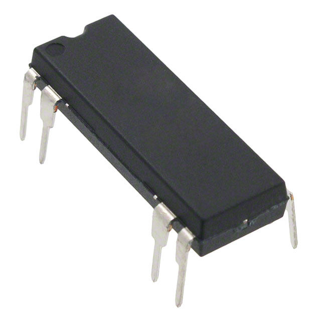
| 产品图片 |
|
| 产品型号 | LMC6442AIMX/NOPB |
| rohs | 无铅 / 符合限制有害物质指令(RoHS)规范要求 |
| 产品系列 | - |
| 供应商器件封装 | 8-SOIC |
| 其它名称 | 296-35442-6 |
| 包装 | Digi-Reel® |
| 压摆率 | 0.0041 V/µs |
| 增益带宽积 | 10.5kHz |
| 安装类型 | 表面贴装 |
| 封装/外壳 | 8-SOIC(0.154",3.90mm 宽) |
| 工作温度 | -40°C ~ 85°C |
| 放大器类型 | 通用 |
| 标准包装 | 1 |
| 电压-电源,单/双 (±) | 1.8 V ~ 11 V, ±0.9 V ~ 5.5 V |
| 电压-输入失调 | 1.5mV |
| 电流-电源 | 1.9µA |
| 电流-输入偏置 | 0.005pA |
| 电流-输出/通道 | 2.1mA |
| 电路数 | 2 |
| 输出类型 | 满摆幅 |


- 商务部:美国ITC正式对集成电路等产品启动337调查
- 曝三星4nm工艺存在良率问题 高通将骁龙8 Gen1或转产台积电
- 太阳诱电将投资9.5亿元在常州建新厂生产MLCC 预计2023年完工
- 英特尔发布欧洲新工厂建设计划 深化IDM 2.0 战略
- 台积电先进制程称霸业界 有大客户加持明年业绩稳了
- 达到5530亿美元!SIA预计今年全球半导体销售额将创下新高
- 英特尔拟将自动驾驶子公司Mobileye上市 估值或超500亿美元
- 三星加码芯片和SET,合并消费电子和移动部门,撤换高东真等 CEO
- 三星电子宣布重大人事变动 还合并消费电子和移动部门
- 海关总署:前11个月进口集成电路产品价值2.52万亿元 增长14.8%


PDF Datasheet 数据手册内容提取
LMC6442 www.ti.com SNOS013E–SEPTEMBER1997–REVISEDMARCH2013 LMC6442 Dual Micropower Rail-to-Rail Output Single Supply Operational Amplifier CheckforSamples:LMC6442 FEATURES DESCRIPTION 1 • (Typical,V =2.2V) The LMC6442 is ideal for battery powered systems, 2 S where very low supply current (less than one • OutputSwingtoWithin30mVofSupplyRail microamp per amplifier) and Rail-to-Rail output swing • HighVoltageGain103dB is required. It is characterized for 2.2V to 10V • GainBandwidthProduct9.5KHz operation, and at 2.2V supply, the LMC6442 is ideal for single (Li-Ion) or two cell (NiCad or alkaline) • Ensuredfor:2.2V,5V,10V batterysystems. • LowSupplyCurrent0.95µA/Amplifier The LMC6442 is designed for battery powered • InputVoltageRange−0.3VtoV+-0.9V systems that require long service life through low • 2.1µW/AmplifierPowerConsumption supply current, such as smoke and gas detectors, • StableforA ≥+2orA ≤ −1 andpagerorpersonalcommunicationssystems. V V Operation from single supply is enhanced by the wide APPLICATIONS commonmodeinputvoltagerangewhichincludesthe ground (or negative supply) for ground sensing • PortableInstruments applications. Very low (5 fA, typical) input bias current • Smoke/Gas/CO/FireDetectors and near constant supply current over supply voltage • Pagers/CellPhones enhance the LMC6442's performance near the end- • Instrumentation of-lifebatteryvoltage. • Thermostats Designed for closed loop gains of greater than plus two (or minus one), the amplifier has typically 9.5 • OccupancySensors KHzGBWP(GainBandwidthProduct).Unitygaincan • Cameras be used with a simple compensation circuit, which • ActiveBadges also allows capacitive loads of up to 300 pF to be driven, as described in the Application Information section. Connection Diagram TopView Figure1. 8-PinSOIC/PDIPPackage SeePackageNumbersD0008A,P0008E Thesedeviceshavelimitedbuilt-inESDprotection.Theleadsshouldbeshortedtogetherorthedeviceplacedinconductivefoam duringstorageorhandlingtopreventelectrostaticdamagetotheMOSgates. 1 Pleasebeawarethatanimportantnoticeconcerningavailability,standardwarranty,anduseincriticalapplicationsof TexasInstrumentssemiconductorproductsanddisclaimerstheretoappearsattheendofthisdatasheet. Alltrademarksarethepropertyoftheirrespectiveowners. 2 PRODUCTIONDATAinformationiscurrentasofpublicationdate. Copyright©1997–2013,TexasInstrumentsIncorporated Products conform to specifications per the terms of the Texas Instruments standard warranty. Production processing does not necessarilyincludetestingofallparameters.
LMC6442 SNOS013E–SEPTEMBER1997–REVISEDMARCH2013 www.ti.com Absolute Maximum Ratings (1)(2) ESDTolerance (3) 2kV DifferentialInputVoltage ±SupplyVoltages VoltageatInput/OutputPin (V+)+0.3V,(V−)−0.3V SupplyVoltage(V+−V−): 16V CurrentatInputPin (4) ±5mA CurrentatOutputPin(5) (6) ±30mA LeadTemp.(soldering10sec) 260°C StorageTemp.Range: −65°Cto+150°C JunctionTemp. (7) 150°C (1) AbsoluteMaximumRatingsindicatelimitsbeyondwhichdamagetothedevicemayoccur.OperatingRatingsindicateconditionsfor whichthedeviceisintendedtobefunctional,butspecificperformanceisnotensured.Forensuredspecificationsandthetest conditions,seetheElectricalCharacteristics. (2) IfMilitary/Aerospacespecifieddevicesarerequired,pleasecontacttheTISalesOffice/Distributorsforavailabilityandspecifications. (3) Humanbodymodel,1.5kΩinserieswith100pF. (4) Limitinginputpincurrentisonlynecessaryforinputvoltagesthatexceedabsolutemaximuminputvoltageratings. (5) Appliestobothsingle-supplyandsplit-supplyoperation.Continuousshortcircuitoperationatelevatedambienttemperaturecanresultin exceedingthemaximumallowedjunctiontemperatureof150°C.Outputcurrentsinexcessof±30mAoverlongtermmayadversely affectreliability. (6) DonotshortcircuitoutputtoV+,whenV+isgreaterthan13Vorreliabilitywillbeadverselyaffected. (7) ThemaximumpowerdissipationisafunctionofT ,θ ,andT .Themaximumallowablepowerdissipationatanyambient J(MAX) JA A temperatureisP =(T -T )/θ .AllnumbersapplyforpackagessoldereddirectlyintoaPCboard. D J(MAX) A JA Operating Ratings (1) SupplyVoltage 1.8V≤V ≤11V S JunctionTemperatureRange:LMC6442AI,LMC6442I −40°C<T <+85°C J ThermalResistance(θ ) D0008APackage,8-pinSurfaceMount 193°C/W JA P0008EPackage,8-pinMoldedDIP 115°C/W (1) AbsoluteMaximumRatingsindicatelimitsbeyondwhichdamagetothedevicemayoccur.OperatingRatingsindicateconditionsfor whichthedeviceisintendedtobefunctional,butspecificperformanceisnotensured.Forensuredspecificationsandthetest conditions,seetheElectricalCharacteristics. 2.2V Electrical Characteristics Unlessotherwisespecified,alllimitsensuredforT =25°C,V+=2.2V,V−=0V,V =V =V+/2,andR =1MΩtoV+/2. J CM O L Boldfacelimitsapplyatthetemperatureextremes. Parameter TestConditions Typ (1) LMLCim6i4t4(22)AI LLMimC6it4(422)I Units DCElectricalCharacteristics V InputOffsetVoltage ±3 ±7 mV OS −0.75 ±4 ±8 max TCV Temp.coefficientofinput OS 0.4 µV/°C offsetvoltage I InputBiasCurrent See (3) pA B 0.005 4 4 max InputOffsetCurrent See (3) pA I 0.0025 2 2 OS max CMRR CommonModeRejection −0.1V≤V ≤0.5V 92 67 67 dBmin CM Ratio 67 67 C CommonModeInput 4.7 pF IN Capacitance PSRR PowerSupplyRejection V =2.5Vto10V 75 75 dB S 95 Ratio 75 75 min (1) TypicalValuesrepresentthemostlikelyparametricnorm. (2) Alllimitsarespecifiedbytestingorstatisticalanalysisunlessotherwisespecified. (3) Limitsspecifiedbydesign. 2 SubmitDocumentationFeedback Copyright©1997–2013,TexasInstrumentsIncorporated ProductFolderLinks:LMC6442
LMC6442 www.ti.com SNOS013E–SEPTEMBER1997–REVISEDMARCH2013 2.2V Electrical Characteristics (continued) Unlessotherwisespecified,alllimitsensuredforT =25°C,V+=2.2V,V−=0V,V =V =V+/2,andR =1MΩtoV+/2. J CM O L Boldfacelimitsapplyatthetemperatureextremes. Parameter TestConditions Typ (1) LMLCim6i4t4(22)AI LLMimC6it4(422)I Units V InputCommon-Mode 1.05 1.05 V CM 1.3 VoltageRange 0.95 0.95 min CMRR≥50dB −0.3 −0.2 −0.2 V 0 0 max A LargeSignalVoltageGain Sourcing (4) 100 V Sinking (4) 94 dB min V =0.22Vto2V 103 80 80 O V OutputSwing V =100mV (5) 2.15 2.15 V O ID 2.18 2.15 2.15 min V =−100mV (5) 22 60 60 mV ID 60 60 max I OutputShortCircuit Sourcing,V =100mV (6) (5) 50 18 18 SC ID Current 17 17 µA Sinking,V =−100mV (6) (5) 50 20 20 min ID 19 19 I SupplyCurrent R =open 1.90 2.4 2.6 S L (2amplifiers) 3.0 3.2 µA max V+=1.8V,R =open 2.10 L ACElectricalCharacteristics SR SlewRate (7) 2.2 V/ms GBWP Gain-BandwidthProduct 9.5 KHz φ PhaseMargin See (8) 63 deg m (4) R connectedtoV+/2.ForSourcingTest,V >V+/2.ForSinkingtests,V <V+/2. L O O (5) V isdifferentialinputvoltagereferencedtoinvertinginput. ID (6) Outputshortedtogroundforsourcing,andshortedtoV+forsinkingshortcircuitcurrenttest. (7) Slewrateisthesloweroftherisingandfallingslewrates. (8) SeetheTypicalPerformanceCharacteristicsandApplicationsInformationsectionsformoredetails. 5V Electrical Characteristics Unlessotherwisespecified,alllimitsensuredforT =25°C,V+=5V,V−=0V,V =V =V+/2,andR =1MΩtoV+/2. J CM O L Boldfacelimitsapplyatthetemperatureextremes. Parameter TestConditions Typ (1) LMLCim6i4t4(22)AI LLMimC6it4(422)I Units DCElectricalCharacteristics V InputOffsetVoltage ±3 ±7 mV OS −0.75 ±4 ±8 max TCV Temp.coefficientofinput 0.4 µV/°C OS offsetvoltage I InputBiasCurrent See (3) pA B 0.005 4 4 max InputOffsetCurrent See (3) pA I 0.0025 2 2 OS max CMRR CommonModeRejection −0.1V≤V ≤3.5V 102 70 70 dBmin CM Ratio 70 70 C CommonModeInput 4.1 pF IN Capacitance PSRR PowerSupplyRejection V =2.5Vto10V 75 75 dB S 95 Ratio 75 75 min (1) TypicalValuesrepresentthemostlikelyparametricnorm. (2) Alllimitsarespecifiedbytestingorstatisticalanalysisunlessotherwisespecified. (3) Limitsspecifiedbydesign. Copyright©1997–2013,TexasInstrumentsIncorporated SubmitDocumentationFeedback 3 ProductFolderLinks:LMC6442
LMC6442 SNOS013E–SEPTEMBER1997–REVISEDMARCH2013 www.ti.com 5V Electrical Characteristics (continued) Unlessotherwisespecified,alllimitsensuredforT =25°C,V+=5V,V−=0V,V =V =V+/2,andR =1MΩtoV+/2. J CM O L Boldfacelimitsapplyatthetemperatureextremes. Parameter TestConditions Typ (1) LMLCim6i4t4(22)AI LLMimC6it4(422)I Units V InputCommon-Mode 3.85 3.85 V CM 4.1 VoltageRange 3.75 3.75 min CMRR≥50dB −0.4 −0.2 −0.2 V 0 0 max A LargeSignalVoltageGain Sourcing (4) 100 V Sinking (4) 94 dB min V =0.5Vto4.5V 103 80 80 O V OutputSwing V =100mV (5) 4.99 4.95 4.95 V O ID 4.95 4.95 min V =−100mV (5) 20 50 50 mV ID 50 50 max I OutputShortCircuitCurrent Sourcing,V =100mV (6) (5) 500 300 300 SC ID 200 200 µA Sinking,V =−100mV (6) (5) 350 200 200 min ID 150 150 I SupplyCurrent R =open 1.90 2.4 2.6 µA S L (2amplifiers) 3.0 3.2 max ACElectricalCharacteristics SR SlewRate (7) 4.1 2.5 2.5 V/ms GBWP Gain-BandwidthProduct 10 KHz φ PhaseMargin See (8) 64 deg m THD TotalHarmonicDistortion A =+2,f=100Hz, 0.08 % V R =10MΩ,V =1V L OUT PP (4) R connectedtoV+/2.ForSourcingTest,V >V+/2.ForSinkingtests,V <V+/2. L O O (5) V isdifferentialinputvoltagereferencedtoinvertinginput. ID (6) Outputshortedtogroundforsourcing,andshortedtoV+forsinkingshortcircuitcurrenttest. (7) Slewrateisthesloweroftherisingandfallingslewrates. (8) SeetheTypicalPerformanceCharacteristicsandApplicationsInformationsectionsformoredetails. 10V Electrical Characteristics Unlessotherwisespecified,alllimitsensuredforT =25°C,V+=10V,V−=0V,V =V =V+/2,andR =1MΩtoV+/2. J CM O L Boldfacelimitsapplyatthetemperatureextremes. Parameter TestConditions Typ (1) LMLCim6i4t4(22)AI LLMimC6it4(422)I Units DCElectricalCharacteristics V InputOffsetVoltage ±3 ±7 mV OS −1.5 ±4 ±8 max TCV Temp.coefficientofinput 0.4 µV/°C OS offsetvoltage I InputBiasCurrent See(3) pA B 0.005 4 4 max InputOffsetCurrent See (3) pA I 0.0025 2 2 OS max CMRR CommonModeRejection −0.1V≤V ≤8.5V 105 70 70 dBmin CM Ratio 70 70 C CommonModeInput 3.5 pF IN Capacitance PSRR PowerSupplyRejection V =2.5Vto10V 75 75 dB S 95 Ratio 75 75 min (1) TypicalValuesrepresentthemostlikelyparametricnorm. (2) Alllimitsarespecifiedbytestingorstatisticalanalysisunlessotherwisespecified. (3) Limitsspecifiedbydesign. 4 SubmitDocumentationFeedback Copyright©1997–2013,TexasInstrumentsIncorporated ProductFolderLinks:LMC6442
LMC6442 www.ti.com SNOS013E–SEPTEMBER1997–REVISEDMARCH2013 10V Electrical Characteristics (continued) Unlessotherwisespecified,alllimitsensuredforT =25°C,V+=10V,V−=0V,V =V =V+/2,andR =1MΩtoV+/2. J CM O L Boldfacelimitsapplyatthetemperatureextremes. Parameter TestConditions Typ (1) LMLCim6i4t4(22)AI LLMimC6it4(422)I Units V InputCommon-Mode 8.85 8.85 V CM 9.1 VoltageRange 8.75 8.75 min CMRR≥50dB −0.4 −0.2 −0.2 V 0 0 max A LargeSignalVoltageGain Sourcing (4) 120 V Sinking (4) 100 dB min V =0.5Vto9.5V 104 80 80 O V OutputSwing V =100mV (5) 9.99 9.97 9.97 V O ID 9.97 9.97 min V =−100mV (5) 22 50 50 mV ID 50 50 max I OutputShortCircuit Sourcing,V =100mV (6) (5) 2100 1200 1200 SC ID Current 1000 1000 µA Sinking,V =−100mV (6) (5) 900 600 600 min ID 500 500 I SupplyCurrent R =open 1.90 2.4 2.6 µA S L (2amplifiers) 3.0 3.2 max ACElectricalCharacteristics SR SlewRate(7) 4.1 2.5 2.5 V/ms GBWP Gain-BandwidthProduct 10.5 KHz φ PhaseMargin See (8) 68 deg m e Input-ReferredVoltage R =open 170 nV/√Hz n L Noise f=10Hz i Input-ReferredCurrent R =open 0.0002 pA/√Hz n L Noise f=10Hz CrosstalkRejection See (9) 85 dB (4) R connectedtoV+/2.ForSourcingTest,V >V+/2.ForSinkingtests,V <V+/2. L O O (5) V isdifferentialinputvoltagereferencedtoinvertinginput. ID (6) Outputshortedtogroundforsourcing,andshortedtoV+forsinkingshortcircuitcurrenttest. (7) Slewrateisthesloweroftherisingandfallingslewrates. (8) SeetheTypicalPerformanceCharacteristicsandApplicationsInformationsectionsformoredetails. (9) Inputreferred,V+=10VandR =10MΩconnectedto5V.Eachampexcitedinturnwith1KHztoproduceabout10V output. L PP Copyright©1997–2013,TexasInstrumentsIncorporated SubmitDocumentationFeedback 5 ProductFolderLinks:LMC6442
LMC6442 SNOS013E–SEPTEMBER1997–REVISEDMARCH2013 www.ti.com Typical Performance Characteristics V =5V,SingleSupply,T =25°Cunlessotherwisespecified S A TotalSupplyCurrent TotalSupplyCurrent vs. vs. SupplyVoltage SupplyVoltage(NegativeInputOverdrive) Figure2. Figure3. TotalSupplyCurrent InputBiasCurrent vs. vs. SupplyVoltage(PositiveInputOverdrive) Temperature Figure4. Figure. OffsetVoltage OffsetVoltage vs. vs. CommonModeVoltage(V =2.2V) CommonModeVoltage(V =5V) S S Figure5. Figure6. 6 SubmitDocumentationFeedback Copyright©1997–2013,TexasInstrumentsIncorporated ProductFolderLinks:LMC6442
LMC6442 www.ti.com SNOS013E–SEPTEMBER1997–REVISEDMARCH2013 Typical Performance Characteristics (continued) V =5V,SingleSupply,T =25°Cunlessotherwisespecified S A OffsetVoltage SwingTowardsV− vs. vs. CommonModeVoltage(V =10V) SupplyVoltage S Figure7. Figure8. SwingTowardsV+ SwingFromRail(s) vs. vs. SupplyVoltage Temperature Figure9. Figure10. OutputSourceCurrent OutputSinkCurrent vs. vs. OutputVoltage OutputVoltage Figure11. Figure12. Copyright©1997–2013,TexasInstrumentsIncorporated SubmitDocumentationFeedback 7 ProductFolderLinks:LMC6442
LMC6442 SNOS013E–SEPTEMBER1997–REVISEDMARCH2013 www.ti.com Typical Performance Characteristics (continued) V =5V,SingleSupply,T =25°Cunlessotherwisespecified S A MaximumOutputVoltage LargeSignalVoltageGain vs. vs. LoadResistance SupplyVoltage Figure13. Figure14. OpenLoopGain/Phase OpenLoopGain/Phase vs. vs. Frequency FrequencyForVariousC (Z =1MΩIIC ) L L L Figure15. Figure16. OpenLoopGain/Phase GainBandwidthProduct vs. vs. FrequencyForVariousC (Z =100KΩIIC ) SupplyVoltage L L L Figure17. Figure18. 8 SubmitDocumentationFeedback Copyright©1997–2013,TexasInstrumentsIncorporated ProductFolderLinks:LMC6442
LMC6442 www.ti.com SNOS013E–SEPTEMBER1997–REVISEDMARCH2013 Typical Performance Characteristics (continued) V =5V,SingleSupply,T =25°Cunlessotherwisespecified S A PhaseMargin(WorstCase) CMRR vs. vs. SupplyVoltage Frequency Figure19. Figure20. PSRR PositiveSlewRate vs. vs. Frequency SupplyVoltage Figure21. Figure22. NegativeSlewRate Cross-TalkRejection vs. vs. SupplyVoltage Frequency Figure23. Figure24. Copyright©1997–2013,TexasInstrumentsIncorporated SubmitDocumentationFeedback 9 ProductFolderLinks:LMC6442
LMC6442 SNOS013E–SEPTEMBER1997–REVISEDMARCH2013 www.ti.com Typical Performance Characteristics (continued) V =5V,SingleSupply,T =25°Cunlessotherwisespecified S A InputVoltageNoise OutputImpedance vs. vs. Frequency Frequency Figure25. Figure26. THD+N THD+N vs. vs. Frequency Amplitude Figure27. Figure28. MaximumOutputSwing vs. SmallSignalStepResponse Frequency (A =+2)(C =12pF,100pF) V L Figure29. Figure30. 10 SubmitDocumentationFeedback Copyright©1997–2013,TexasInstrumentsIncorporated ProductFolderLinks:LMC6442
LMC6442 www.ti.com SNOS013E–SEPTEMBER1997–REVISEDMARCH2013 Typical Performance Characteristics (continued) V =5V,SingleSupply,T =25°Cunlessotherwisespecified S A LargeSignalStepResponse SmallSignalStepResponse (A =+2)(C =100pF) (A =−1)(C =1MΩII100pF,200pF) V L V L Figure31. Figure32. SmallSignalStepResponse LargeSignalStepResponse (A =+1)ForVariousC (A =+1)(C =200pF) V L V L Figure33. Figure34. Copyright©1997–2013,TexasInstrumentsIncorporated SubmitDocumentationFeedback 11 ProductFolderLinks:LMC6442
LMC6442 SNOS013E–SEPTEMBER1997–REVISEDMARCH2013 www.ti.com APPLICATIONS INFORMATION USING LMC6442 IN UNITY GAIN APPLICATIONS LMC6442 is optimized for maximum bandwidth and minimal external components when operating at a minimum closed loop gain of +2 (or −1). However, it is also possible to operate the device in a unity gain configuration by addingexternalcompensationasshowninFigure35: Figure35. A =+1OperationbyaddingC andR V C C Using this compensation technique it is possible to drive capacitive loads of up to 300 pF without causing oscillations (see the Typical Performance Characteristics for step response plots). This compensation can also be used with other gain settings in order to improve stability, especially when driving capacitive loads (for optimumperformance,R andC mayneedtobeadjusted). C C USING “T” NETWORK Compromises need to be made whenever high gain inverting stages need to achieve a high input impedance as well. This is especially important in low current applications which tend to deal with high resistance values. Using a traditional inverting amplifier, gain is inversely proportional to the resistor value tied between the inverting terminal and input while the input impedance is equal to this value. For example, in order to build an inverting amplifier with an input impedance of 10MΩ and a gain of 100, one needs to come up with a feedback resistor of 1000MΩ -anexpensivetask. Analternatesolutionistousea“T” Networkinthefeedbackpath,asshowninFigure36. Closedloopgain,A isgivenby: V (1) Figure36. “T”NetworkUsedtoReplaceHighValueResistor It must be noted, however, that using this scheme, the realizable bandwidth would be less than the theoretical maximum.Withfeedbackfactor,β,definedas: (2) BW(−3dB)≈GBWP•β (3) In this case, assuming a GBWP of about 10 KHz, the expected BW would be around 50 Hz (vs. 100 Hz with the conventionalinvertingamplifier). 12 SubmitDocumentationFeedback Copyright©1997–2013,TexasInstrumentsIncorporated ProductFolderLinks:LMC6442
LMC6442 www.ti.com SNOS013E–SEPTEMBER1997–REVISEDMARCH2013 Looking at the problem from a different view, with R defined by A •Rin, one could select a value for R in the “T” F V NetworkandthendetermineR1basedonthisselection: (4) Figure37. “T”NetworkValuesforVariousValuesofR Forconvenience,Figure37showsR1vs.R fordifferentvaluesofR. F DESIGN CONSIDERATIONS FOR CAPACITIVE LOADS As with many other opamps, the LMC6442 is more stable at higher closed loop gains when driving a capacitive load.Figure38showsminimumclosedloopgainversusloadcapacitance,toachievelessthan10%overshootin the output small signal response. In addition, the LMC6442 is more stable when it provides more output current totheloadandwhenitsoutputvoltagedoesnotswingclosetoV−. The LMC6442 is more tolerant to capacitive loads when the equivalent output load resistance is lowered or when output voltage is 1V or greater from the V− supply. The capacitive load drive capability is also improved by adding an isolating resistor in series with the load and the output of the device. Figure 39 shows the value of this resistorforvariouscapacitiveloads(A =−1),whilelimitingtheoutputtolessthan10%overshoot. V Referring to the Typical Performance Characteristics plot of Phase Margin (Worst Case) vs. Supply Voltage, note that Phase Margin increases as the equivalent output load resistance is lowered. This plot shows the expected Phase Margin when the device output is very close to V−, which is the least stable condition of operation. Comparing this Phase Margin value to the one read off the Open Loop Gain/Phase vs. Frequency plot, one can predict the improvement in Phase Margin if the output does not swing close to V−. This dependence of Phase Marginonoutputvoltageisminimizedaslongastheoutputload,R ,isabout1MΩorless. L Output Phase Reversal: The LMC6442 is immune against this behavior even when the input voltages exceed thecommonmodevoltagerange. Output Time Delay: Due to the ultra low power consumption of the device, there could be as long as 2.5 ms of timedelayfromwhenpowerisappliedtowhenthedeviceoutputreachesitsfinalvalue. Copyright©1997–2013,TexasInstrumentsIncorporated SubmitDocumentationFeedback 13 ProductFolderLinks:LMC6442
LMC6442 SNOS013E–SEPTEMBER1997–REVISEDMARCH2013 www.ti.com Figure38. MinimumOperatingGainvs.CapacitiveLoad Figure39. IsolatingResistorValuevsCapacitiveLoad 14 SubmitDocumentationFeedback Copyright©1997–2013,TexasInstrumentsIncorporated ProductFolderLinks:LMC6442
LMC6442 www.ti.com SNOS013E–SEPTEMBER1997–REVISEDMARCH2013 Application Circuits V+=5V:I <10µA,f/V =4.3(Hz/V) S C Figure40. MicropowerSingleSupplyVoltagetoFrequencyConverter Figure41. GainStagewithCurrentBoosting Copyright©1997–2013,TexasInstrumentsIncorporated SubmitDocumentationFeedback 15 ProductFolderLinks:LMC6442
LMC6442 SNOS013E–SEPTEMBER1997–REVISEDMARCH2013 www.ti.com Figure42. OffsetNullingSchemes 16 SubmitDocumentationFeedback Copyright©1997–2013,TexasInstrumentsIncorporated ProductFolderLinks:LMC6442
LMC6442 www.ti.com SNOS013E–SEPTEMBER1997–REVISEDMARCH2013 REVISION HISTORY ChangesfromRevisionD(March2013)toRevisionE Page • ChangedlayoutofNationalDataSheettoTIformat.......................................................................................................... 16 Copyright©1997–2013,TexasInstrumentsIncorporated SubmitDocumentationFeedback 17 ProductFolderLinks:LMC6442
PACKAGE OPTION ADDENDUM www.ti.com 22-Feb-2020 PACKAGING INFORMATION Orderable Device Status Package Type Package Pins Package Eco Plan Lead/Ball Finish MSL Peak Temp Op Temp (°C) Device Marking Samples (1) Drawing Qty (2) (6) (3) (4/5) LMC6442AIM/NOPB ACTIVE SOIC D 8 95 Green (RoHS SN Level-1-260C-UNLIM -40 to 85 LMC64 & no Sb/Br) 42AIM LMC6442AIMX/NOPB ACTIVE SOIC D 8 2500 Green (RoHS SN Level-1-260C-UNLIM -40 to 85 LMC64 & no Sb/Br) 42AIM LMC6442IM/NOPB ACTIVE SOIC D 8 95 Green (RoHS SN Level-1-260C-UNLIM -40 to 85 LMC64 & no Sb/Br) 42IM LMC6442IMX/NOPB ACTIVE SOIC D 8 2500 Green (RoHS Call TI | SN Level-1-260C-UNLIM -40 to 85 LMC64 & no Sb/Br) 42IM LMC6442IN/NOPB ACTIVE PDIP P 8 40 Green (RoHS Call TI | SN Level-1-NA-UNLIM -40 to 85 LMC6442 & no Sb/Br) IN (1) The marketing status values are defined as follows: ACTIVE: Product device recommended for new designs. LIFEBUY: TI has announced that the device will be discontinued, and a lifetime-buy period is in effect. NRND: Not recommended for new designs. Device is in production to support existing customers, but TI does not recommend using this part in a new design. PREVIEW: Device has been announced but is not in production. Samples may or may not be available. OBSOLETE: TI has discontinued the production of the device. (2) RoHS: TI defines "RoHS" to mean semiconductor products that are compliant with the current EU RoHS requirements for all 10 RoHS substances, including the requirement that RoHS substance do not exceed 0.1% by weight in homogeneous materials. Where designed to be soldered at high temperatures, "RoHS" products are suitable for use in specified lead-free processes. TI may reference these types of products as "Pb-Free". RoHS Exempt: TI defines "RoHS Exempt" to mean products that contain lead but are compliant with EU RoHS pursuant to a specific EU RoHS exemption. Green: TI defines "Green" to mean the content of Chlorine (Cl) and Bromine (Br) based flame retardants meet JS709B low halogen requirements of <=1000ppm threshold. Antimony trioxide based flame retardants must also meet the <=1000ppm threshold requirement. (3) MSL, Peak Temp. - The Moisture Sensitivity Level rating according to the JEDEC industry standard classifications, and peak solder temperature. (4) There may be additional marking, which relates to the logo, the lot trace code information, or the environmental category on the device. (5) Multiple Device Markings will be inside parentheses. Only one Device Marking contained in parentheses and separated by a "~" will appear on a device. If a line is indented then it is a continuation of the previous line and the two combined represent the entire Device Marking for that device. (6) Lead/Ball Finish - Orderable Devices may have multiple material finish options. Finish options are separated by a vertical ruled line. Lead/Ball Finish values may wrap to two lines if the finish value exceeds the maximum column width. Addendum-Page 1
PACKAGE OPTION ADDENDUM www.ti.com 22-Feb-2020 Important Information and Disclaimer:The information provided on this page represents TI's knowledge and belief as of the date that it is provided. TI bases its knowledge and belief on information provided by third parties, and makes no representation or warranty as to the accuracy of such information. Efforts are underway to better integrate information from third parties. TI has taken and continues to take reasonable steps to provide representative and accurate information but may not have conducted destructive testing or chemical analysis on incoming materials and chemicals. TI and TI suppliers consider certain information to be proprietary, and thus CAS numbers and other limited information may not be available for release. In no event shall TI's liability arising out of such information exceed the total purchase price of the TI part(s) at issue in this document sold by TI to Customer on an annual basis. Addendum-Page 2
PACKAGE MATERIALS INFORMATION www.ti.com 10-Aug-2016 TAPE AND REEL INFORMATION *Alldimensionsarenominal Device Package Package Pins SPQ Reel Reel A0 B0 K0 P1 W Pin1 Type Drawing Diameter Width (mm) (mm) (mm) (mm) (mm) Quadrant (mm) W1(mm) LMC6442AIMX/NOPB SOIC D 8 2500 330.0 12.4 6.5 5.4 2.0 8.0 12.0 Q1 LMC6442IMX/NOPB SOIC D 8 2500 330.0 12.4 6.5 5.4 2.0 8.0 12.0 Q1 PackMaterials-Page1
PACKAGE MATERIALS INFORMATION www.ti.com 10-Aug-2016 *Alldimensionsarenominal Device PackageType PackageDrawing Pins SPQ Length(mm) Width(mm) Height(mm) LMC6442AIMX/NOPB SOIC D 8 2500 367.0 367.0 35.0 LMC6442IMX/NOPB SOIC D 8 2500 367.0 367.0 35.0 PackMaterials-Page2
PACKAGE OUTLINE D0008A SOIC - 1.75 mm max height SCALE 2.800 SMALL OUTLINE INTEGRATED CIRCUIT C SEATING PLANE .228-.244 TYP [5.80-6.19] .004 [0.1] C A PIN 1 ID AREA 6X .050 [1.27] 8 1 2X .189-.197 [4.81-5.00] .150 NOTE 3 [3.81] 4X (0 -15 ) 4 5 8X .012-.020 B .150-.157 [0.31-0.51] .069 MAX [3.81-3.98] .010 [0.25] C A B [1.75] NOTE 4 .005-.010 TYP [0.13-0.25] 4X (0 -15 ) SEE DETAIL A .010 [0.25] .004-.010 0 - 8 [0.11-0.25] .016-.050 [0.41-1.27] DETAIL A (.041) TYPICAL [1.04] 4214825/C 02/2019 NOTES: 1. Linear dimensions are in inches [millimeters]. Dimensions in parenthesis are for reference only. Controlling dimensions are in inches. Dimensioning and tolerancing per ASME Y14.5M. 2. This drawing is subject to change without notice. 3. This dimension does not include mold flash, protrusions, or gate burrs. Mold flash, protrusions, or gate burrs shall not exceed .006 [0.15] per side. 4. This dimension does not include interlead flash. 5. Reference JEDEC registration MS-012, variation AA. www.ti.com
EXAMPLE BOARD LAYOUT D0008A SOIC - 1.75 mm max height SMALL OUTLINE INTEGRATED CIRCUIT 8X (.061 ) [1.55] SYMM SEE DETAILS 1 8 8X (.024) [0.6] SYMM (R.002 ) TYP [0.05] 5 4 6X (.050 ) [1.27] (.213) [5.4] LAND PATTERN EXAMPLE EXPOSED METAL SHOWN SCALE:8X SOLDER MASK SOLDER MASK METAL OPENING OPENING METAL UNDER SOLDER MASK EXPOSED METAL EXPOSED METAL .0028 MAX .0028 MIN [0.07] [0.07] ALL AROUND ALL AROUND NON SOLDER MASK SOLDER MASK DEFINED DEFINED SOLDER MASK DETAILS 4214825/C 02/2019 NOTES: (continued) 6. Publication IPC-7351 may have alternate designs. 7. Solder mask tolerances between and around signal pads can vary based on board fabrication site. www.ti.com
EXAMPLE STENCIL DESIGN D0008A SOIC - 1.75 mm max height SMALL OUTLINE INTEGRATED CIRCUIT 8X (.061 ) [1.55] SYMM 1 8 8X (.024) [0.6] SYMM (R.002 ) TYP [0.05] 5 4 6X (.050 ) [1.27] (.213) [5.4] SOLDER PASTE EXAMPLE BASED ON .005 INCH [0.125 MM] THICK STENCIL SCALE:8X 4214825/C 02/2019 NOTES: (continued) 8. Laser cutting apertures with trapezoidal walls and rounded corners may offer better paste release. IPC-7525 may have alternate design recommendations. 9. Board assembly site may have different recommendations for stencil design. www.ti.com
None
IMPORTANTNOTICEANDDISCLAIMER TI PROVIDES TECHNICAL AND RELIABILITY DATA (INCLUDING DATASHEETS), DESIGN RESOURCES (INCLUDING REFERENCE DESIGNS), APPLICATION OR OTHER DESIGN ADVICE, WEB TOOLS, SAFETY INFORMATION, AND OTHER RESOURCES “AS IS” AND WITH ALL FAULTS, AND DISCLAIMS ALL WARRANTIES, EXPRESS AND IMPLIED, INCLUDING WITHOUT LIMITATION ANY IMPLIED WARRANTIES OF MERCHANTABILITY, FITNESS FOR A PARTICULAR PURPOSE OR NON-INFRINGEMENT OF THIRD PARTY INTELLECTUAL PROPERTY RIGHTS. These resources are intended for skilled developers designing with TI products. You are solely responsible for (1) selecting the appropriate TI products for your application, (2) designing, validating and testing your application, and (3) ensuring your application meets applicable standards, and any other safety, security, or other requirements. These resources are subject to change without notice. TI grants you permission to use these resources only for development of an application that uses the TI products described in the resource. Other reproduction and display of these resources is prohibited. No license is granted to any other TI intellectual property right or to any third party intellectual property right. TI disclaims responsibility for, and you will fully indemnify TI and its representatives against, any claims, damages, costs, losses, and liabilities arising out of your use of these resources. TI’s products are provided subject to TI’s Terms of Sale (www.ti.com/legal/termsofsale.html) or other applicable terms available either on ti.com or provided in conjunction with such TI products. TI’s provision of these resources does not expand or otherwise alter TI’s applicable warranties or warranty disclaimers for TI products. Mailing Address: Texas Instruments, Post Office Box 655303, Dallas, Texas 75265 Copyright © 2020, Texas Instruments Incorporated