ICGOO在线商城 > 集成电路(IC) > PMIC - 稳压器 - 线性 > LM78L12ACM
 Datasheet下载
- 型号: LM78L12ACM
- 制造商: Texas Instruments
- 库位|库存: xxxx|xxxx
- 要求:
| 数量阶梯 | 香港交货 | 国内含税 |
| +xxxx | $xxxx | ¥xxxx |
查看当月历史价格
查看今年历史价格
LM78L12ACM产品简介:
ICGOO电子元器件商城为您提供LM78L12ACM由Texas Instruments设计生产,在icgoo商城现货销售,并且可以通过原厂、代理商等渠道进行代购。 LM78L12ACM价格参考。Texas InstrumentsLM78L12ACM封装/规格:PMIC - 稳压器 - 线性, Linear Voltage Regulator IC Positive Fixed 1 Output 12V 100mA 8-SOIC。您可以下载LM78L12ACM参考资料、Datasheet数据手册功能说明书,资料中有LM78L12ACM 详细功能的应用电路图电压和使用方法及教程。
LM78L12ACM 是由德州仪器 (Texas Instruments) 生产的一款线性稳压器,属于 PMIC(电源管理集成电路)类别。它具有固定输出电压 12V,并且是一款低功耗、三端正电压调节器。

 应用场景

 1. 便携式电子设备
   LM78L12ACM 适用于需要稳定 12V 输出的小型便携式设备。例如:
   - 手持式测量仪器:如万用表、温度计等,这些设备通常需要稳定的电源供应以确保测量精度。
   - 小型通信设备:如对讲机、无线模块等,12V 的稳定输出可以为这些设备提供可靠的电源支持。

 2. 汽车电子
   在汽车电子系统中,LM78L12ACM 可以为各种辅助电路提供稳定的 12V 电源。例如:
   - 车载音响系统:为放大器、收音机等提供稳定的电源,确保音频质量不受电源波动影响。
   - 传感器和执行器:为车内的各种传感器(如温度传感器、压力传感器)以及执行器(如电动窗控制器)提供稳定的电源。

 3. 工业控制
   在工业环境中,LM78L12ACM 可用于为各种控制系统中的组件提供稳定的电源。例如:
   - PLC(可编程逻辑控制器)模块:为 I/O 模块、通信接口等提供稳定的 12V 电源,确保系统的可靠运行。
   - 传感器和变送器:为工业传感器(如光电传感器、接近开关)提供稳定的电源,确保信号的准确传输。

 4. 消费电子产品
   在一些消费电子产品中,LM78L12ACM 也可以发挥重要作用。例如:
   - LED 照明系统:为 LED 驱动电路提供稳定的 12V 电源,确保照明效果的一致性和稳定性。
   - 小型家电:如风扇、加湿器等,12V 的稳定输出可以为电机和其他控制电路提供可靠的电源。

 5. 实验室和教育用途
   LM78L12ACM 还常用于实验室和教育领域,作为教学和实验中的电源模块。例如:
   - 实验电源板:为学生或研究人员提供稳定的 12V 电源,方便进行各种电路测试和实验。
   - 教学演示设备:为教学用的电子设备提供稳定的电源,确保实验结果的准确性。

总的来说,LM78L12ACM 由于其简单易用、稳定可靠的特点,广泛应用于需要 12V 稳定电源的各种场合,尤其是在对电源要求不高但需要高稳定性的应用场景中表现尤为出色。
| 参数 | 数值 |
| 产品目录 | 集成电路 (IC)半导体 |
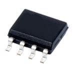
| 描述 | IC REG LDO 12V 0.1A 8SOIC线性稳压器 3-Terminal Positive Regulators 8-SOIC 0 to 125 |
| 产品分类 | |
| 品牌 | Texas Instruments |
| 产品手册 | |
| 产品图片 |
|
| rohs | 否含铅 / 不符合限制有害物质指令(RoHS)规范要求 |
| 产品系列 | 电源管理 IC,线性稳压器,Texas Instruments LM78L12ACM- |
| 数据手册 | |
| 产品型号 | LM78L12ACM |
| 产品种类 | 线性稳压器 |
| 供应商器件封装 | 8-SOIC |
| 包装 | 管件 |
| 商标 | Texas Instruments |
| 安装类型 | 表面贴装 |
| 安装风格 | SMD/SMT |
| 封装 | Tube |
| 封装/外壳 | 8-SOIC(0.154",3.90mm 宽) |
| 封装/箱体 | SOIC-8 Narrow |
| 工作温度 | 0°C ~ 125°C |
| 工厂包装数量 | 95 |
| 最大功率耗散 | 750 mW |
| 最大工作温度 | + 125 C |
| 最大输入电压 | 35 V |
| 最小工作温度 | 0 C |
| 最小输入电压 | 13.7 V |
| 极性 | Positive |
| 标准包装 | 95 |
| 电压-跌落(典型值) | - |
| 电压-输入 | 13.7 V ~ 35 V |
| 电压-输出 | 12V |
| 电流-输出 | 100mA |
| 电流-限制(最小值) | - |
| 稳压器拓扑 | 正,固定式 |
| 稳压器数 | 1 |
| 系列 | LM78L12 |
| 线路调整率 | 180 mV |
| 设计资源 | http://www.digikey.com/product-highlights/cn/zh/texas-instruments-webench-design-center/3176 |
| 负载调节 | 100 mV |
| 输出电压 | 12 V |
| 输出电流 | 0.1 A |
| 输出端数量 | 1 |
| 输出类型 | Fixed |


PDF Datasheet 数据手册内容提取
Product Sample & Technical Tools & Support & Reference Folder Buy Documents Software Community Design LM78L05,LM78L09 LM78L12,LM78L15,LM78L62 SNVS754K–JANUARY2000–REVISEDDECEMBER2016 LM78Lxx 100-mA Fixed Output Linear Regulator 1 Features 3 Description • InputVoltageupto30V The LM78Lxx series of three terminal positive 1 regulators is available with several fixed output • OutputVoltageTolerancesof ±5%Overthe voltages, making them useful in a wide range of TemperatureRange applications. Used as a Zener-diode and resistor • AvailableOutputVoltages:5V,6.2V,8.2V,9V, combination replacement, the LM78Lxx usually 12V,and15V provides an effective output impedance improvement of two orders of magnitude and lower quiescent • OutputCurrentof100mA current. These regulators can provide local, on-card • OutputTransistorSafeAreaProtection regulation, eliminating distribution problems • InternalThermalOverloadProtection associated with single-point regulation. The available • InternalShort-CircuitCurrentLimit voltages allow the LM78Lxx to be used in logic systems, instrumentation, HiFi, and other solid-state • NoExternalComponents electronicequipment. • AvailableinTinyDSBGAPackage The LM78Lxx is available in the plastic TO-92 (LP) • Availablein3-PinTO-92and8-PinSOICLow package, the SOIC (D) package, and a chip-sized ProfilePackages package (8-Bump DSBGA) using TI's DSBGA package technology. With adequate heat sinking, the 2 Applications regulator can deliver 100-mA output current. Current • BatteryChargers limiting is included to limit the peak output current to a safe value. Safe area protection for the output • PortableInstrumentation transistors is provided to limit internal power • LEDLighting dissipation. If internal power dissipation is too high for • LowWattagePowerSupplies the heat sinking provided, the thermal shutdown circuitpreventstheICfromoverheating. PackageOptions See AN-1112 DSBGA Wafer Level Chip Scale Package (SNVA009) for DSBGA Considerations. For more information on the TO-92 package, see TO-92 DSBGA PackingOptions/OrderingInstructions (SNOA072). 8-Pin 1 3 DeviceInformation(1) 2 1 PARTNUMBER PACKAGE BODYSIZE(NOM) LM78L05,LM78L09 DSBGA(8) 1.30mm×1.30mm SOIC 8-Pin LM78L05,LM78L12, SOIC(8) 3.90mm×4.90mm LM78L15 LM78L05,LM78L12, TO-92 TO-92(3) 3.70mm×4.70mm LM78L15,LM78L62 3-Pin 1 (1) For all available packages, see the orderable addendum at Not to scale theendofthedatasheet. FixedOutputRegulatorCircuit 1 An IMPORTANT NOTICE at the end of this data sheet addresses availability, warranty, changes, use in safety-critical applications, intellectualpropertymattersandotherimportantdisclaimers.PRODUCTIONDATA.
LM78L05,LM78L09 LM78L12,LM78L15,LM78L62 SNVS754K–JANUARY2000–REVISEDDECEMBER2016 www.ti.com Table of Contents 1 Features.................................................................. 1 7.3 FeatureDescription.................................................11 2 Applications........................................................... 1 7.4 DeviceFunctionalModes........................................11 3 Description............................................................. 1 8 ApplicationandImplementation........................ 12 4 RevisionHistory..................................................... 2 8.1 ApplicationInformation............................................12 8.2 TypicalApplications................................................12 5 PinConfigurationandFunctions......................... 3 9 PowerSupplyRecommendations...................... 16 6 Specifications......................................................... 4 10 Layout................................................................... 16 6.1 AbsoluteMaximumRatings......................................4 6.2 ESDRatings..............................................................4 10.1 LayoutGuidelines.................................................16 6.3 RecommendedOperatingConditions.......................4 10.2 LayoutExample....................................................16 6.4 ThermalInformation..................................................4 11 DeviceandDocumentationSupport................. 17 6.5 ElectricalCharacteristics—LM78L05......................5 11.1 DocumentationSupport........................................17 6.6 ElectricalCharacteristics—LM78L09......................5 11.2 RelatedLinks........................................................17 6.7 ElectricalCharacteristics—LM78L12......................6 11.3 ReceivingNotificationofDocumentationUpdates17 6.8 ElectricalCharacteristics—LM78L15......................6 11.4 CommunityResources..........................................17 6.9 ElectricalCharacteristics—LM78L62......................7 11.5 Trademarks...........................................................17 6.10 TypicalCharacteristics............................................8 11.6 ElectrostaticDischargeCaution............................17 7 DetailedDescription............................................ 10 11.7 Glossary................................................................17 7.1 Overview.................................................................10 12 Mechanical,Packaging,andOrderable Information........................................................... 18 7.2 FunctionalBlockDiagram.......................................10 4 Revision History NOTE:Pagenumbersforpreviousrevisionsmaydifferfrompagenumbersinthecurrentversion. ChangesfromRevisionJ(December2013)toRevisionK Page • AddedApplicationssection,DeviceInformationtable,PinConfigurationandFunctionssection,ESDRatingstable, RecommendedOperatingConditionstable,DetailedDescriptionsection,ApplicationandImplementationsection, PowerSupplyRecommendationssection,Layoutsection,DeviceandDocumentationSupportsection,and Mechanical,Packaging,andOrderableInformationsection.................................................................................................. 1 • DeletedLM78L82fromthedatasheet................................................................................................................................... 1 • AddedThermalInformationtable........................................................................................................................................... 1 • DeletedLeadtemperature(soldering)information................................................................................................................. 4 • ChangedR valuesforD(SOIC)From:180To:128.8,LP(TO-92)from230to158.7,andYPB(DSBGA)From: θJA 230.9To108.4....................................................................................................................................................................... 4 • ChangedR valuesforLP(TO-92)From:60To75.2......................................................................................................... 4 θJC ChangesfromRevisionI(April2013)toRevisionJ Page • AddedtheAIsuffix................................................................................................................................................................. 5 2 SubmitDocumentationFeedback Copyright©2000–2016,TexasInstrumentsIncorporated ProductFolderLinks:LM78L05 LM78L09LM78L12 LM78L15 LM78L62
LM78L05,LM78L09 LM78L12,LM78L15,LM78L62 www.ti.com SNVS754K–JANUARY2000–REVISEDDECEMBER2016 5 Pin Configuration and Functions YPBPackage DPackage 8-PinDSBGA 8-PinSOIC TopView TopView A B C VOUT 1 8 VIN 3 VOUT NC GND GND 2 7 GND GND 3 6 GND NC 4 5 NC 2 VOUT GND Not to scale 1 VIN VIN NC Not to scale LPPackage 3-PinTO-92 BottomView 3 VIN 2 GND 1 VOUT Not to scale PinFunctions PIN I/O DESCRIPTION NAME DSBGA SOIC TO-92 GND C2,C3 2,3,6,7 2 — Ground NC B3,C1 4,5 — — Noconnection VIN A1,B1 8 3 I Inputsupplyvoltagepin VOUT A2,A3 1 1 O Outputvoltagepin Copyright©2000–2016,TexasInstrumentsIncorporated SubmitDocumentationFeedback 3 ProductFolderLinks:LM78L05 LM78L09LM78L12 LM78L15 LM78L62
LM78L05,LM78L09 LM78L12,LM78L15,LM78L62 SNVS754K–JANUARY2000–REVISEDDECEMBER2016 www.ti.com 6 Specifications 6.1 Absolute Maximum Ratings overoperatingfree-airtemperaturerange(unlessotherwisenoted)(1)(2) MIN MAX UNIT Inputvoltage 35 V Powerdissipation Internallylimited LM78LxxACZ(TO-92) 0 125 LM78LxxACM(SOIC) 0 125 Operatingjunctiontemperature,T °C J LM78LxxAIM(SOIC) –40 125 LM78LxxITP(thinDSBGA) –40 85 Storagetemperature,T –65 150 °C stg (1) StressesbeyondthoselistedunderAbsoluteMaximumRatingsmaycausepermanentdamagetothedevice.Thesearestressratings only,whichdonotimplyfunctionaloperationofthedeviceattheseoranyotherconditionsbeyondthoseindicatedunderRecommended OperatingConditions.Exposuretoabsolute-maximum-ratedconditionsforextendedperiodsmayaffectdevicereliability. (2) IfMilitary/Aerospacespecifieddevicesarerequired,pleasecontacttheTexasInstrumentsSalesOffice/Distributorsforavailabilityand specifications. 6.2 ESD Ratings VALUE UNIT V Electrostaticdischarge Human-bodymodel(HBM),(1) ±1000 V (ESD) (1) Humanbodymodel,1.5kΩinserieswith100pF. 6.3 Recommended Operating Conditions overoperatingfree-airtemperaturerange(unlessotherwisenoted) MIN NOM MAX UNIT Inputvoltage 30 V Continuousoutputcurrent 100 mA LM78LxxACZ(TO-92) 0 125 LM78LxxACM(SOIC) 0 125 T Junctiontemperature °C J LM78LxxAIM(SOIC) –40 125 LM78LxxITP(DSBGA) –40 85 6.4 Thermal Information LM78Lxx THERMALMETRIC(1) D(SOIC) LP(TO-92) YPB(DSBGA) UNIT 8PINS 3PINS 8PINS R Junction-to-ambientthermalresistance 128.8 158.7 108.4 °C/W θJA R Junction-to-case(top)thermalresistance 76 75.2 1.3 °C/W θJC(top) R Junction-to-boardthermalresistance 69.3 n/a 31.4 °C/W θJB ψ Junction-to-topcharacterizationparameter 26.3 30.2 4.5 °C/W JT ψ Junction-to-boardcharacterizationparameter 68.8 138.2 31.4 °C/W JB R Junction-to-case(bottom)thermalresistance — — — °C/W θJC(bot) (1) Formoreinformationabouttraditionalandnewthermalmetrics,seetheSemiconductorandICPackageThermalMetricsapplication report. 4 SubmitDocumentationFeedback Copyright©2000–2016,TexasInstrumentsIncorporated ProductFolderLinks:LM78L05 LM78L09LM78L12 LM78L15 LM78L62
LM78L05,LM78L09 LM78L12,LM78L15,LM78L62 www.ti.com SNVS754K–JANUARY2000–REVISEDDECEMBER2016 6.5 Electrical Characteristics — LM78L05 TypicalvaluesapplyforT =25°C,MinimumandMaximumlimitsapplyfortheentireoperatingtemperaturerangeofthe J package(1)(2),I =40mA,C =0.33µF,C =0.1µF,V =10V(unlessotherwisenoted). O I O IN PARAMETER TESTCONDITIONS MIN TYP MAX UNIT T =25°C 4.8 5 5.2 J V Outputvoltage V =7Vto20V,I =1mAto40mA(3) 4.75 5.25 V O IN O I =1mAto70mA(3) 4.75 5.25 O V =7Vto20V,T =25°C 18 75 IN J Lineregulation V =8Vto20V,T =25°C 10 54 IN J ΔV mV O I =1mAto100mA,T =25°C 20 60 O J Loadregulation I =1mAto40mA,T =25°C 5 30 O J I Quiescentcurrent T =25°C 3 5 mA Q J V =8Vto20V 1 IN ΔI Quiescentcurrentchange mA Q I =1mAto40mA 0.1 O V Outputnoisevoltage f=10Hzto100kHz(4) 40 µV n ΔV /ΔV Ripplerejection f=120Hz,V =8Vto16V,T =25°C 47 62 dB IN O IN J I Peakoutputcurrent 140 mA PK Averageoutputvoltagetemperature ΔV /ΔT I =5mA –0.65 mV/°C O coefficient O Minimumvalueofinputvoltage V T =25°C 6.7 7 V IN(MIN) requiredtomaintainlineregulation J (1) Fortheoperatingrangesofeachpackage,seeAbsoluteMaximumRatings. (2) LimitsareensuredbyproductiontestingorcorrelationtechniquesusingstandardStatisticalQualityControl(SQC)methods. (3) Powerdissipation≤0.75W. (4) Recommendedminimumloadcapacitanceof0.01µFtolimithigh-frequencynoise. 6.6 Electrical Characteristics — LM78L09 TypicalvaluesapplyforT =25°C,MinimumandMaximumlimitsapplyfortheentireoperatingtemperaturerangeofthe J package(1)(2),I =40mA,C =0.33µF,C =0.1µF,V =15V(unlessotherwisenoted). O I O IN PARAMETER TESTCONDITIONS MIN TYP MAX UNIT T =25°C 8.64 9 9.36 J V Outputvoltage V =11.5Vto24V,I =1mAto40mA(3) 8.55 9.45 V O IN O I =1mAto70mA(3) 8.55 9.45 O V =11.5Vto24V,T =25°C 100 200 IN J Lineregulation V =13Vto24V,T =25°C 90 150 IN J ΔV mV O I =1mAto100mA,T =25°C 20 90 O J Loadregulation I =1mAto40mA,T =25°C 10 45 O J I Quiescentcurrent T =25°C 2 5.5 mA Q J V =11.5Vto24V 1.5 IN ΔI Quiescentcurrentchange mA Q I =1mAto40mA 0.1 O V Outputnoisevoltage 70 µV n ΔV /ΔV Ripplerejection f=120Hz,V =15Vto25V,T =25°C 38 44 dB IN O IN J I Peakoutputcurrent 140 mA PK Averageoutputvoltagetemperature ΔV /ΔT I =5mA –0.9 mV/°C O coefficient O Minimumvalueofinputvoltage V 10.7 V IN(MIN) requiredtomaintainlineregulation (1) Fortheoperatingrangesofeachpackage,seeAbsoluteMaximumRatings. (2) LimitsareensuredbyproductiontestingorcorrelationtechniquesusingstandardStatisticalQualityControl(SQC)methods. (3) Powerdissipation≤0.75W. Copyright©2000–2016,TexasInstrumentsIncorporated SubmitDocumentationFeedback 5 ProductFolderLinks:LM78L05 LM78L09LM78L12 LM78L15 LM78L62
LM78L05,LM78L09 LM78L12,LM78L15,LM78L62 SNVS754K–JANUARY2000–REVISEDDECEMBER2016 www.ti.com 6.7 Electrical Characteristics — LM78L12 TypicalvaluesapplyforT =25°C,MinimumandMaximumlimitsapplyfortheentireoperatingtemperaturerangeofthe J package(1)(2),I =40mA,C =0.33µF,C =0.1µF,V =19V(unlessotherwisenoted). O I O IN PARAMETER TESTCONDITIONS MIN TYP MAX UNIT T =25°C 11.5 12 12.5 J V Outputvoltage V =14.5Vto27V,I =1mAto40mA(3) 11.4 12.6 V O IN O I =1mAto70mA(3) 11.4 12.6 O V =14.5Vto27V,T =25°C 30 180 IN J Lineregulation V =16Vto27V,T =25°C 20 110 IN J ΔV mV O I =1mAto100mA,T =25°C 30 100 O J Loadregulation I =1mAto40mA,T =25°C 10 50 O J I Quiescentcurrent T =25°C 3 5 mA Q J V =16Vto27V 1 IN ΔI Quiescentcurrentchange mA Q I =1mAto40mA 0.1 O V Outputnoisevoltage 80 µV n ΔV /ΔV Ripplerejection f=120Hz,V =15Vto25V,T =25°C 40 54 dB IN O IN J I Peakoutputcurrent 140 mA PK Averageoutputvoltagetemperature ΔV /ΔT I =5mA –1 mV/°C O coefficient O Minimumvalueofinputvoltage V T =25°C 13.7 14.5 V IN(MIN) requiredtomaintainlineregulation J (1) Fortheoperatingrangesofeachpackage,seeAbsoluteMaximumRatings. (2) LimitsareensuredbyproductiontestingorcorrelationtechniquesusingstandardStatisticalQualityControl(SQC)methods. (3) Powerdissipation≤0.75W. 6.8 Electrical Characteristics — LM78L15 TypicalvaluesapplyforT =25°C,MinimumandMaximumlimitsapplyfortheentireoperatingtemperaturerangeofthe J package(1)(2),I =40mA,C =0.33µF,C =0.1µF,V =23V(unlessotherwisenoted). O I O IN PARAMETER TESTCONDITIONS MIN TYP MAX UNIT T =25°C 14.4 15 15.6 J V Outputvoltage V =17.5Vto30V,I =1mAto40mA(3) 14.25 15.75 V O IN O I =1mAto70mA(3) 14.25 15.75 O V =17.5Vto30V,T =25°C 37 250 IN J Lineregulation V =20Vto30V,T =25°C 25 140 IN J ΔV mV O I =1mAto100mA,T =25°C 35 150 O J Loadregulation I =1mAto40mA,T =25°C 12 75 O J I Quiescentcurrent T =25°C 3 5 mA Q J V =20Vto30V 1 IN ΔI Quiescentcurrentchange mA Q I =1mAto40mA 0.1 O V Outputnoisevoltage 90 µV n ΔV /ΔV Ripplerejection f=120Hz,V =18.5Vto28.5V,T =25°C 37 51 dB IN O IN J I Peakoutputcurrent 140 mA PK Averageoutputvoltagetemperature ΔV /ΔT I =5mA –1.3 mV/°C O coefficient O Minimumvalueofinputvoltage V T =25°C 16.7 17.5 V IN(MIN) requiredtomaintainlineregulation J (1) Fortheoperatingrangesofeachpackage,seeAbsoluteMaximumRatings. (2) LimitsareensuredbyproductiontestingorcorrelationtechniquesusingstandardStatisticalQualityControl(SQC)methods. (3) Powerdissipation≤0.75W. 6 SubmitDocumentationFeedback Copyright©2000–2016,TexasInstrumentsIncorporated ProductFolderLinks:LM78L05 LM78L09LM78L12 LM78L15 LM78L62
LM78L05,LM78L09 LM78L12,LM78L15,LM78L62 www.ti.com SNVS754K–JANUARY2000–REVISEDDECEMBER2016 6.9 Electrical Characteristics — LM78L62 TypicalvaluesapplyforT =25°C,MinimumandMaximumlimitsapplyfortheentireoperatingtemperaturerangeofthe J package(1)(2),I =40mA,C =0.33µF,C =0.1µF,V =12V(unlessotherwisenoted). O I O IN PARAMETER TESTCONDITIONS MIN TYP MAX UNIT T =25°C 5.95 6.2 6.45 J V Outputvoltage V =8.5Vto20V,I =1mAto40mA(3) 5.9 6.5 V O IN O I =1mAto70mA(3) 5.9 6.5 O V =8.5Vto20V,T =25°C 65 175 IN J Lineregulation V =9Vto20V,T =25°C 55 125 IN J ΔV mV O I =1mAto100mA,T =25°C 13 80 O J Loadregulation I =1mAto40mA,T =25°C 6 40 O J I Quiescentcurrent T =25°C 2 5.5 mA Q J V =8Vto20V 1.5 IN ΔI Quiescentcurrentchange mA Q I =1mAto40mA 0.1 O V Outputnoisevoltage f=10Hzto100kHz(4) 50 µV n ΔV /ΔV Ripplerejection f=120Hz,V =10Vto20V,T =25°C 40 46 dB IN O IN J I Peakoutputcurrent 140 mA PK Averageoutputvoltagetemperature ΔV /ΔT I =5mA –0.75 mV/°C O coefficient O Minimumvalueofinputvoltage V 7.9 V IN(MIN) requiredtomaintainlineregulation (1) Fortheoperatingrangesofeachpackage,seeAbsoluteMaximumRatings. (2) LimitsareensuredbyproductiontestingorcorrelationtechniquesusingstandardStatisticalQualityControl(SQC)methods. (3) Powerdissipation≤0.75W. (4) Recommendedminimumloadcapacitanceof0.01µFtolimithigh-frequencynoise. Copyright©2000–2016,TexasInstrumentsIncorporated SubmitDocumentationFeedback 7 ProductFolderLinks:LM78L05 LM78L09LM78L12 LM78L15 LM78L62
LM78L05,LM78L09 LM78L12,LM78L15,LM78L62 SNVS754K–JANUARY2000–REVISEDDECEMBER2016 www.ti.com 6.10 Typical Characteristics LPPackage Figure1.MaximumAveragePowerDissipation Figure2.PeakOutputCurrent Figure3.DropoutVoltage Figure4.RippleRejection Figure5.OutputImpedance Figure6.QuiescentCurrent 8 SubmitDocumentationFeedback Copyright©2000–2016,TexasInstrumentsIncorporated ProductFolderLinks:LM78L05 LM78L09LM78L12 LM78L15 LM78L62
LM78L05,LM78L09 LM78L12,LM78L15,LM78L62 www.ti.com SNVS754K–JANUARY2000–REVISEDDECEMBER2016 Typical Characteristics (continued) Figure7.QuiescentCurrent Copyright©2000–2016,TexasInstrumentsIncorporated SubmitDocumentationFeedback 9 ProductFolderLinks:LM78L05 LM78L09LM78L12 LM78L15 LM78L62
LM78L05,LM78L09 LM78L12,LM78L15,LM78L62 SNVS754K–JANUARY2000–REVISEDDECEMBER2016 www.ti.com 7 Detailed Description 7.1 Overview The LM78Lxx series of positive regulators is available in the following fixed output voltages: 5 V, 6.2 V, 8.2 V, 9 V, 12 V, and 15 V. The regulator can be configured to an adjustable output by connecting the GND pin to the center of a resistive voltage divider as shown in Figure 10. In this configuration, the fixed output voltage acts as thereferencevoltageacrossR1allowingtheoutputtobeadjustedbychangingtheresistor. 7.2 Functional Block Diagram 10 SubmitDocumentationFeedback Copyright©2000–2016,TexasInstrumentsIncorporated ProductFolderLinks:LM78L05 LM78L09LM78L12 LM78L15 LM78L62
LM78L05,LM78L09 LM78L12,LM78L15,LM78L62 www.ti.com SNVS754K–JANUARY2000–REVISEDDECEMBER2016 7.3 Feature Description 7.3.1 LoadRegulation These devices regulate the voltage between the VOUT and GND pins, and can be made adjustable by using a resistivevoltagedivider.Theoutputvoltagetoleranceis ±5%overtemperature. 7.3.2 Protection The LM78Lxx series of regulators has internal thermal overload protection that automatically shuts off the device if the operating temperature becomes too high. There is also internal short-circuit current limit and output transistorsafeareaprotectionthatshutsdownthedeviceiftheoutputcurrentbecomestoohigh. 7.4 Device Functional Modes 7.4.1 NormalOperation The VOUT pin sources current necessary to set the voltage on VOUT at a fixed voltage above the GND pin. See SpecificationsforV ofeachdevice. O 7.4.2 Shutdown Thedeviceautomaticallyshutsdowniftheoutputcurrentoritsinternaltemperaturebecomestoohigh. Copyright©2000–2016,TexasInstrumentsIncorporated SubmitDocumentationFeedback 11 ProductFolderLinks:LM78L05 LM78L09LM78L12 LM78L15 LM78L62
LM78L05,LM78L09 LM78L12,LM78L15,LM78L62 SNVS754K–JANUARY2000–REVISEDDECEMBER2016 www.ti.com 8 Application and Implementation NOTE Information in the following applications sections is not part of the TI component specification, and TI does not warrant its accuracy or completeness. TI’s customers are responsible for determining suitability of components for their purposes. Customers should validateandtesttheirdesignimplementationtoconfirmsystemfunctionality. 8.1 Application Information These devices are versatile and high-performance regulators with a wide temperature range and tight line and loadregulation.Aninputcapacitorisrequirediftheregulatorisplacedmorethan3inchesfromthepowersupply filter.TIrecommendsaminimumloadcapacitanceof0.01 µFtolimithighfrequency. 8.2 Typical Applications 8.2.1 FixedOutputRegulator *Requirediftheregulatorislocatedmorethan3inchesfromthepowersupplyfilter. **Recommendedminimumloadcapacitanceof0.01µFtolimithigh-frequencynoise. Figure8. FixedOutputRegulatorCircuit 8.2.1.1 DesignRequirements The device component count is very minimal. No external components are usually required. However, TI recommendsinputoroutputcapacitorsdependingonthedistancebetweenthedeviceandthepowersupplyand ifextrafilteringisneededattheoutput. Theoutputvoltageissetbasedontheselectionofthetworesistors(R1andR2),asshowninFigure14. 8.2.1.2 DetailedDesignProcedure 8.2.1.2.1 InputCapacitor Aninputcapacitorisrequirediftheregulatorisplacedmorethan3inchesfromthepowersupplyfilter.A0.33-µF capacitorontheinputissuitableformostapplications. 8.2.1.2.2 OutputCapacitor TIrecommendsaminimumloadcapacitanceof0.01µFtolimithigh-frequencynoise. 12 SubmitDocumentationFeedback Copyright©2000–2016,TexasInstrumentsIncorporated ProductFolderLinks:LM78L05 LM78L09LM78L12 LM78L15 LM78L62
LM78L05,LM78L09 LM78L12,LM78L15,LM78L62 www.ti.com SNVS754K–JANUARY2000–REVISEDDECEMBER2016 Typical Applications (continued) 8.2.1.3 ApplicationCurve 1.9 1.8 V) al ( 1.7 nti e Differ 1.6 put 1.5 ut O ut - 1.4 p n I 1.3 25qC 1.2 0 20 40 60 80 100 Load Current (mA) Figure9. LM78LxxDropout 8.2.2 OtherApplicationCircuits Figure 10 to Figure 14 show application circuit examples using the LM78Lxx devices. Customers must fully validate and test these circuits before implementing a design based on these examples. Unless otherwise noted, thedesignproceduresinFixedOutputRegulatorareapplicabletothesedesigns. V =5V+(5V/R1+I )×R2* O Q *The5VrepresentsthefixedoutputvoltageoftheLM78L05.IfusingoneoftheotherLM78Lxxdevices,usethat fixedoutputvoltagevaluewhencalculatingV . O I <5V/(3×R1) Q Loadregulation(L )ofLM78L05≈(R1+R2)/R1 R Figure10. AdjustableOutputRegulatorCircuit Copyright©2000–2016,TexasInstrumentsIncorporated SubmitDocumentationFeedback 13 ProductFolderLinks:LM78L05 LM78L09LM78L12 LM78L15 LM78L62
LM78L05,LM78L09 LM78L12,LM78L15,LM78L62 SNVS754K–JANUARY2000–REVISEDDECEMBER2016 www.ti.com Typical Applications (continued) I =(V /R1)+I OUT O Q I =1.5mAoverlineandloadchanges Q Figure11. CurrentRegulatorCircuit *Solidtantalum **HeatsinkQ1 ***Optional:Improvesripplerejectionandtransientresponse. LoadRegulation=0.6%,I =0mAto250mApulsedwitht =50ms. L ON Figure12. 5-V,500-mARegulatorWithShort-CircuitProtectionCircuit 14 SubmitDocumentationFeedback Copyright©2000–2016,TexasInstrumentsIncorporated ProductFolderLinks:LM78L05 LM78L09LM78L12 LM78L15 LM78L62
LM78L05,LM78L09 LM78L12,LM78L15,LM78L62 www.ti.com SNVS754K–JANUARY2000–REVISEDDECEMBER2016 Typical Applications (continued) *Solidtantalum Figure13. ±15-V,100-mADualPowerSupplyCircuit *Solidtantalum V =V +5V,R1=(–V /I ) O G IN Q(LM78L05) V =5V(R2/R4)for(R2+R3)=(R4+R5) O A0.5-Voutputwillcorrespondto(R2/R4)=0.1,(R3/R4)=0.9 Figure14. VariableOutputRegulatorCircuit(0.5Vto18V) Copyright©2000–2016,TexasInstrumentsIncorporated SubmitDocumentationFeedback 15 ProductFolderLinks:LM78L05 LM78L09LM78L12 LM78L15 LM78L62
LM78L05,LM78L09 LM78L12,LM78L15,LM78L62 SNVS754K–JANUARY2000–REVISEDDECEMBER2016 www.ti.com 9 Power Supply Recommendations The linear regulator input supply must be well regulated and kept at a voltage level to not exceed the maximum input to output voltage differential allowed by the device. The minimum dropout voltage (V – V ) must be met IN O with extra headroom when possible to keep the output well regulated. A 0.33-µF or higher capacitor must be placedattheinputtobypassnoise. 10 Layout 10.1 Layout Guidelines For the best overall performance, some layout guidelines may be disregarded. Place all circuit components on the same side of the circuit board and as near as practical to the respective linear regulator pins. Traces must be kept short and wide to reduce the amount of parasitic elements in the system. The actual width and thickness of tracesdependsonthecurrentcarryingcapabilityandheatdissipationrequiredbytheendsystem. 10.2 Layout Example GND U1 C1 C2 V V IN OUT Figure15. LM78LxxExampleCircuitLayout 16 SubmitDocumentationFeedback Copyright©2000–2016,TexasInstrumentsIncorporated ProductFolderLinks:LM78L05 LM78L09LM78L12 LM78L15 LM78L62
LM78L05,LM78L09 LM78L12,LM78L15,LM78L62 www.ti.com SNVS754K–JANUARY2000–REVISEDDECEMBER2016 11 Device and Documentation Support 11.1 Documentation Support 11.1.1 RelatedDocumentation Forrelateddocumentationseethefollowing: • AN-1112DSBGAWaferLevelChipScalePackage (SNVA009) • TO-92PackingOptions/OrderingInstructions (SNOA072). 11.2 Related Links The table below lists quick access links. Categories include technical documents, support and community resources,toolsandsoftware,andquickaccesstosampleorbuy. Table1.RelatedLinks TECHNICAL TOOLS& SUPPORT& PARTS PRODUCTFOLDER SAMPLE&BUY DOCUMENTS SOFTWARE COMMUNITY LM78L05 Clickhere Clickhere Clickhere Clickhere Clickhere LM78L09 Clickhere Clickhere Clickhere Clickhere Clickhere LM78L12 Clickhere Clickhere Clickhere Clickhere Clickhere LM78L15 Clickhere Clickhere Clickhere Clickhere Clickhere LM78L62 Clickhere Clickhere Clickhere Clickhere Clickhere 11.3 Receiving Notification of Documentation Updates To receive notification of documentation updates, navigate to the device product folder on ti.com. In the upper right corner, click on Alert me to register and receive a weekly digest of any product information that has changed.Forchangedetails,reviewtherevisionhistoryincludedinanyreviseddocument. 11.4 Community Resources The following links connect to TI community resources. Linked contents are provided "AS IS" by the respective contributors. They do not constitute TI specifications and do not necessarily reflect TI's views; see TI's Terms of Use. TIE2E™OnlineCommunity TI'sEngineer-to-Engineer(E2E)Community.Createdtofostercollaboration amongengineers.Ate2e.ti.com,youcanaskquestions,shareknowledge,exploreideasandhelp solveproblemswithfellowengineers. DesignSupport TI'sDesignSupport QuicklyfindhelpfulE2Eforumsalongwithdesignsupporttoolsand contactinformationfortechnicalsupport. 11.5 Trademarks E2EisatrademarkofTexasInstruments. Allothertrademarksarethepropertyoftheirrespectiveowners. 11.6 Electrostatic Discharge Caution This integrated circuit can be damaged by ESD. Texas Instruments recommends that all integrated circuits be handled with appropriateprecautions.Failuretoobserveproperhandlingandinstallationprocedurescancausedamage. ESDdamagecanrangefromsubtleperformancedegradationtocompletedevicefailure.Precisionintegratedcircuitsmaybemore susceptibletodamagebecauseverysmallparametricchangescouldcausethedevicenottomeetitspublishedspecifications. 11.7 Glossary SLYZ022—TIGlossary. Thisglossarylistsandexplainsterms,acronyms,anddefinitions. Copyright©2000–2016,TexasInstrumentsIncorporated SubmitDocumentationFeedback 17 ProductFolderLinks:LM78L05 LM78L09LM78L12 LM78L15 LM78L62
LM78L05,LM78L09 LM78L12,LM78L15,LM78L62 SNVS754K–JANUARY2000–REVISEDDECEMBER2016 www.ti.com 12 Mechanical, Packaging, and Orderable Information The following pages include mechanical, packaging, and orderable information. This information is the most current data available for the designated devices. This data is subject to change without notice and revision of thisdocument.Forbrowser-basedversionsofthisdatasheet,refertotheleft-handnavigation. 18 SubmitDocumentationFeedback Copyright©2000–2016,TexasInstrumentsIncorporated ProductFolderLinks:LM78L05 LM78L09LM78L12 LM78L15 LM78L62
PACKAGE OPTION ADDENDUM www.ti.com 14-Jul-2016 PACKAGING INFORMATION Orderable Device Status Package Type Package Pins Package Eco Plan Lead/Ball Finish MSL Peak Temp Op Temp (°C) Device Marking Samples (1) Drawing Qty (2) (6) (3) (4/5) LM78L05ACM NRND SOIC D 8 95 TBD Call TI Call TI 0 to 125 LM78L 05ACM LM78L05ACM/NOPB ACTIVE SOIC D 8 95 Green (RoHS CU SN Level-1-260C-UNLIM 0 to 125 LM78L & no Sb/Br) 05ACM LM78L05ACMX NRND SOIC D 8 2500 TBD Call TI Call TI 0 to 125 LM78L 05ACM LM78L05ACMX/NOPB ACTIVE SOIC D 8 2500 Green (RoHS CU SN Level-1-260C-UNLIM 0 to 125 LM78L & no Sb/Br) 05ACM LM78L05ACZ/LFT1 ACTIVE TO-92 LP 3 2000 Green (RoHS CU SN N / A for Pkg Type 0 to 125 LM78L & no Sb/Br) 05ACZ LM78L05ACZ/LFT3 ACTIVE TO-92 LP 3 2000 Green (RoHS CU SN N / A for Pkg Type 0 to 125 LM78L & no Sb/Br) 05ACZ LM78L05ACZ/LFT4 ACTIVE TO-92 LP 3 2000 Green (RoHS CU SN N / A for Pkg Type 0 to 125 LM78L & no Sb/Br) 05ACZ LM78L05ACZ/LFT7 ACTIVE TO-92 LP 3 2000 Green (RoHS CU SN N / A for Pkg Type 0 to 125 LM78L & no Sb/Br) 05ACZ LM78L05ACZ/NOPB ACTIVE TO-92 LP 3 1800 Green (RoHS CU SN N / A for Pkg Type 0 to 125 LM78L & no Sb/Br) 05ACZ LM78L05AIM/NOPB ACTIVE SOIC D 8 95 Green (RoHS CU SN Level-1-260C-UNLIM -40 to 125 LM78L & no Sb/Br) 05AM LM78L05AIMX/NOPB ACTIVE SOIC D 8 2500 Green (RoHS CU SN Level-1-260C-UNLIM -40 to 125 LM78L & no Sb/Br) 05AM LM78L05ITP/NOPB ACTIVE DSBGA YPB 8 250 Green (RoHS SNAGCU Level-1-260C-UNLIM -40 to 85 P & no Sb/Br) 03 LM78L05ITPX/NOPB ACTIVE DSBGA YPB 8 3000 Green (RoHS SNAGCU Level-1-260C-UNLIM -40 to 85 P & no Sb/Br) 03 LM78L09ITPX/NOPB ACTIVE DSBGA YPB 8 3000 Green (RoHS SNAGCU Level-1-260C-UNLIM -40 to 85 P & no Sb/Br) 02 LM78L12ACM NRND SOIC D 8 95 TBD Call TI Call TI 0 to 125 LM78L 12ACM LM78L12ACM/NOPB ACTIVE SOIC D 8 95 Green (RoHS CU SN Level-1-260C-UNLIM 0 to 125 LM78L & no Sb/Br) 12ACM LM78L12ACMX NRND SOIC D 8 2500 TBD Call TI Call TI 0 to 125 LM78L 12ACM Addendum-Page 1
PACKAGE OPTION ADDENDUM www.ti.com 14-Jul-2016 Orderable Device Status Package Type Package Pins Package Eco Plan Lead/Ball Finish MSL Peak Temp Op Temp (°C) Device Marking Samples (1) Drawing Qty (2) (6) (3) (4/5) LM78L12ACMX/NOPB ACTIVE SOIC D 8 2500 Green (RoHS CU SN Level-1-260C-UNLIM 0 to 125 LM78L & no Sb/Br) 12ACM LM78L12ACZ/LFT3 ACTIVE TO-92 LP 3 2000 Green (RoHS CU SN N / A for Pkg Type 0 to 125 LM78L & no Sb/Br) 12ACZ LM78L12ACZ/LFT4 ACTIVE TO-92 LP 3 2000 Green (RoHS CU SN N / A for Pkg Type 0 to 125 LM78L & no Sb/Br) 12ACZ LM78L12ACZ/LFT7 ACTIVE TO-92 LP 3 2000 Green (RoHS CU SN N / A for Pkg Type 0 to 125 LM78L & no Sb/Br) 12ACZ LM78L12ACZ/NOPB ACTIVE TO-92 LP 3 1800 Green (RoHS CU SN N / A for Pkg Type 0 to 125 LM78L & no Sb/Br) 12ACZ LM78L15ACM NRND SOIC D 8 95 TBD Call TI Call TI 0 to 125 LM78L 15ACM LM78L15ACM/NOPB ACTIVE SOIC D 8 95 Green (RoHS CU SN Level-1-260C-UNLIM 0 to 125 LM78L & no Sb/Br) 15ACM LM78L15ACMX NRND SOIC D 8 2500 TBD Call TI Call TI 0 to 125 LM78L 15ACM LM78L15ACMX/NOPB ACTIVE SOIC D 8 2500 Green (RoHS CU SN Level-1-260C-UNLIM 0 to 125 LM78L & no Sb/Br) 15ACM LM78L15ACZ/LFT4 ACTIVE TO-92 LP 3 2000 Green (RoHS CU SN N / A for Pkg Type 0 to 125 LM78L & no Sb/Br) 15ACZ LM78L15ACZ/NOPB ACTIVE TO-92 LP 3 1800 Green (RoHS CU SN N / A for Pkg Type 0 to 125 LM78L & no Sb/Br) 15ACZ LM78L62ACZ/NOPB ACTIVE TO-92 LP 3 1800 Green (RoHS CU SN N / A for Pkg Type 0 to 125 LM78L & no Sb/Br) 62ACZ (1) The marketing status values are defined as follows: ACTIVE: Product device recommended for new designs. LIFEBUY: TI has announced that the device will be discontinued, and a lifetime-buy period is in effect. NRND: Not recommended for new designs. Device is in production to support existing customers, but TI does not recommend using this part in a new design. PREVIEW: Device has been announced but is not in production. Samples may or may not be available. OBSOLETE: TI has discontinued the production of the device. (2) Eco Plan - The planned eco-friendly classification: Pb-Free (RoHS), Pb-Free (RoHS Exempt), or Green (RoHS & no Sb/Br) - please check http://www.ti.com/productcontent for the latest availability information and additional product content details. TBD: The Pb-Free/Green conversion plan has not been defined. Pb-Free (RoHS): TI's terms "Lead-Free" or "Pb-Free" mean semiconductor products that are compatible with the current RoHS requirements for all 6 substances, including the requirement that lead not exceed 0.1% by weight in homogeneous materials. Where designed to be soldered at high temperatures, TI Pb-Free products are suitable for use in specified lead-free processes. Addendum-Page 2
PACKAGE OPTION ADDENDUM www.ti.com 14-Jul-2016 Pb-Free (RoHS Exempt): This component has a RoHS exemption for either 1) lead-based flip-chip solder bumps used between the die and package, or 2) lead-based die adhesive used between the die and leadframe. The component is otherwise considered Pb-Free (RoHS compatible) as defined above. Green (RoHS & no Sb/Br): TI defines "Green" to mean Pb-Free (RoHS compatible), and free of Bromine (Br) and Antimony (Sb) based flame retardants (Br or Sb do not exceed 0.1% by weight in homogeneous material) (3) MSL, Peak Temp. - The Moisture Sensitivity Level rating according to the JEDEC industry standard classifications, and peak solder temperature. (4) There may be additional marking, which relates to the logo, the lot trace code information, or the environmental category on the device. (5) Multiple Device Markings will be inside parentheses. Only one Device Marking contained in parentheses and separated by a "~" will appear on a device. If a line is indented then it is a continuation of the previous line and the two combined represent the entire Device Marking for that device. (6) Lead/Ball Finish - Orderable Devices may have multiple material finish options. Finish options are separated by a vertical ruled line. Lead/Ball Finish values may wrap to two lines if the finish value exceeds the maximum column width. Important Information and Disclaimer:The information provided on this page represents TI's knowledge and belief as of the date that it is provided. TI bases its knowledge and belief on information provided by third parties, and makes no representation or warranty as to the accuracy of such information. Efforts are underway to better integrate information from third parties. TI has taken and continues to take reasonable steps to provide representative and accurate information but may not have conducted destructive testing or chemical analysis on incoming materials and chemicals. TI and TI suppliers consider certain information to be proprietary, and thus CAS numbers and other limited information may not be available for release. In no event shall TI's liability arising out of such information exceed the total purchase price of the TI part(s) at issue in this document sold by TI to Customer on an annual basis. Addendum-Page 3
PACKAGE MATERIALS INFORMATION www.ti.com 14-Jul-2016 TAPE AND REEL INFORMATION *Alldimensionsarenominal Device Package Package Pins SPQ Reel Reel A0 B0 K0 P1 W Pin1 Type Drawing Diameter Width (mm) (mm) (mm) (mm) (mm) Quadrant (mm) W1(mm) LM78L05ACMX SOIC D 8 2500 330.0 12.4 6.5 5.4 2.0 8.0 12.0 Q1 LM78L05ACMX/NOPB SOIC D 8 2500 330.0 12.4 6.5 5.4 2.0 8.0 12.0 Q1 LM78L05AIMX/NOPB SOIC D 8 2500 330.0 12.4 6.5 5.4 2.0 8.0 12.0 Q1 LM78L05ITP/NOPB DSBGA YPB 8 250 178.0 8.4 1.5 1.5 0.66 4.0 8.0 Q1 LM78L05ITPX/NOPB DSBGA YPB 8 3000 178.0 8.4 1.5 1.5 0.66 4.0 8.0 Q1 LM78L09ITPX/NOPB DSBGA YPB 8 3000 178.0 8.4 1.5 1.5 0.66 4.0 8.0 Q1 LM78L12ACMX SOIC D 8 2500 330.0 12.4 6.5 5.4 2.0 8.0 12.0 Q1 LM78L12ACMX/NOPB SOIC D 8 2500 330.0 12.4 6.5 5.4 2.0 8.0 12.0 Q1 LM78L15ACMX SOIC D 8 2500 330.0 12.4 6.5 5.4 2.0 8.0 12.0 Q1 LM78L15ACMX/NOPB SOIC D 8 2500 330.0 12.4 6.5 5.4 2.0 8.0 12.0 Q1 PackMaterials-Page1
PACKAGE MATERIALS INFORMATION www.ti.com 14-Jul-2016 *Alldimensionsarenominal Device PackageType PackageDrawing Pins SPQ Length(mm) Width(mm) Height(mm) LM78L05ACMX SOIC D 8 2500 367.0 367.0 35.0 LM78L05ACMX/NOPB SOIC D 8 2500 367.0 367.0 35.0 LM78L05AIMX/NOPB SOIC D 8 2500 367.0 367.0 35.0 LM78L05ITP/NOPB DSBGA YPB 8 250 210.0 185.0 35.0 LM78L05ITPX/NOPB DSBGA YPB 8 3000 210.0 185.0 35.0 LM78L09ITPX/NOPB DSBGA YPB 8 3000 210.0 185.0 35.0 LM78L12ACMX SOIC D 8 2500 367.0 367.0 35.0 LM78L12ACMX/NOPB SOIC D 8 2500 367.0 367.0 35.0 LM78L15ACMX SOIC D 8 2500 367.0 367.0 35.0 LM78L15ACMX/NOPB SOIC D 8 2500 367.0 367.0 35.0 PackMaterials-Page2
None
None
None
PACKAGE OUTLINE YPB0008 DSBGA - 0.575 mm max height SCALE 9.000 DIE SIZE BALL GRID ARRAY B E A BALL A1 CORNER D 0.575 MAX C SEATING PLANE 0.15 BALL TYP 0.11 0.05 C 1 TYP C 1 SYMM TYP B D: Max = 1.337 mm, Min =1 .276 mm 0.5 TYP E: Max = 1.337 mm, Min =1 .276 mm A 8X 0.18 1 2 3 0.16 0.015 C A B 0.5 TYP SYMM 4215100/B 07/2016 NOTES: 1. All linear dimensions are in millimeters. Any dimensions in parenthesis are for reference only. Dimensioning and tolerancing per ASME Y14.5M. 2. This drawing is subject to change without notice. www.ti.com
EXAMPLE BOARD LAYOUT YPB0008 DSBGA - 0.575 mm max height DIE SIZE BALL GRID ARRAY (0.5) TYP 8X ( 0.16) 1 2 3 A (0.5) TYP SYMM B C SYMM LAND PATTERN EXAMPLE SCALE:40X ( 0.16) 0.05 MAX METAL UNDER 0.05 MIN METAL SOLDER MASK SOLDER MASK ( 0.16) OPENING SOLDER MASK OPENING NON-SOLDER MASK DEFINED SOLDER MASK (PREFERRED) DEFINED SOLDER MASK DETAILS NOT TO SCALE 4215100/B 07/2016 NOTES: (continued) 3. Final dimensions may vary due to manufacturing tolerance considerations and also routing constraints. See Texas Instruments Literature No. SNVA009 (www.ti.com/lit/snva009). www.ti.com
EXAMPLE STENCIL DESIGN YPB0008 DSBGA - 0.575 mm max height DIE SIZE BALL GRID ARRAY (0.5) TYP (R0.05) TYP 8X ( 0.3) 1 2 3 A (0.5) TYP SYMM B METAL TYP C SYMM SOLDER PASTE EXAMPLE BASED ON 0.125mm THICK STENCIL SCALE:50X 4215100/B 07/2016 NOTES: (continued) 4. Laser cutting apertures with trapezoidal walls and rounded corners may offer better paste release. www.ti.com
IMPORTANTNOTICEFORTIDESIGNINFORMATIONANDRESOURCES TexasInstrumentsIncorporated(‘TI”)technical,applicationorotherdesignadvice,servicesorinformation,including,butnotlimitedto, referencedesignsandmaterialsrelatingtoevaluationmodules,(collectively,“TIResources”)areintendedtoassistdesignerswhoare developingapplicationsthatincorporateTIproducts;bydownloading,accessingorusinganyparticularTIResourceinanyway,you (individuallyor,ifyouareactingonbehalfofacompany,yourcompany)agreetouseitsolelyforthispurposeandsubjecttothetermsof thisNotice. TI’sprovisionofTIResourcesdoesnotexpandorotherwisealterTI’sapplicablepublishedwarrantiesorwarrantydisclaimersforTI products,andnoadditionalobligationsorliabilitiesarisefromTIprovidingsuchTIResources.TIreservestherighttomakecorrections, enhancements,improvementsandotherchangestoitsTIResources. Youunderstandandagreethatyouremainresponsibleforusingyourindependentanalysis,evaluationandjudgmentindesigningyour applicationsandthatyouhavefullandexclusiveresponsibilitytoassurethesafetyofyourapplicationsandcomplianceofyourapplications (andofallTIproductsusedinorforyourapplications)withallapplicableregulations,lawsandotherapplicablerequirements.You representthat,withrespecttoyourapplications,youhaveallthenecessaryexpertisetocreateandimplementsafeguardsthat(1) anticipatedangerousconsequencesoffailures,(2)monitorfailuresandtheirconsequences,and(3)lessenthelikelihoodoffailuresthat mightcauseharmandtakeappropriateactions.YouagreethatpriortousingordistributinganyapplicationsthatincludeTIproducts,you willthoroughlytestsuchapplicationsandthefunctionalityofsuchTIproductsasusedinsuchapplications.TIhasnotconductedany testingotherthanthatspecificallydescribedinthepublisheddocumentationforaparticularTIResource. Youareauthorizedtouse,copyandmodifyanyindividualTIResourceonlyinconnectionwiththedevelopmentofapplicationsthatinclude theTIproduct(s)identifiedinsuchTIResource.NOOTHERLICENSE,EXPRESSORIMPLIED,BYESTOPPELOROTHERWISETO ANYOTHERTIINTELLECTUALPROPERTYRIGHT,ANDNOLICENSETOANYTECHNOLOGYORINTELLECTUALPROPERTY RIGHTOFTIORANYTHIRDPARTYISGRANTEDHEREIN,includingbutnotlimitedtoanypatentright,copyright,maskworkright,or otherintellectualpropertyrightrelatingtoanycombination,machine,orprocessinwhichTIproductsorservicesareused.Information regardingorreferencingthird-partyproductsorservicesdoesnotconstitutealicensetousesuchproductsorservices,orawarrantyor endorsementthereof.UseofTIResourcesmayrequirealicensefromathirdpartyunderthepatentsorotherintellectualpropertyofthe thirdparty,oralicensefromTIunderthepatentsorotherintellectualpropertyofTI. TIRESOURCESAREPROVIDED“ASIS”ANDWITHALLFAULTS.TIDISCLAIMSALLOTHERWARRANTIESOR REPRESENTATIONS,EXPRESSORIMPLIED,REGARDINGTIRESOURCESORUSETHEREOF,INCLUDINGBUTNOTLIMITEDTO ACCURACYORCOMPLETENESS,TITLE,ANYEPIDEMICFAILUREWARRANTYANDANYIMPLIEDWARRANTIESOF MERCHANTABILITY,FITNESSFORAPARTICULARPURPOSE,ANDNON-INFRINGEMENTOFANYTHIRDPARTYINTELLECTUAL PROPERTYRIGHTS. TISHALLNOTBELIABLEFORANDSHALLNOTDEFENDORINDEMNIFYYOUAGAINSTANYCLAIM,INCLUDINGBUTNOT LIMITEDTOANYINFRINGEMENTCLAIMTHATRELATESTOORISBASEDONANYCOMBINATIONOFPRODUCTSEVENIF DESCRIBEDINTIRESOURCESOROTHERWISE.INNOEVENTSHALLTIBELIABLEFORANYACTUAL,DIRECT,SPECIAL, COLLATERAL,INDIRECT,PUNITIVE,INCIDENTAL,CONSEQUENTIALOREXEMPLARYDAMAGESINCONNECTIONWITHOR ARISINGOUTOFTIRESOURCESORUSETHEREOF,ANDREGARDLESSOFWHETHERTIHASBEENADVISEDOFTHE POSSIBILITYOFSUCHDAMAGES. YouagreetofullyindemnifyTIanditsrepresentativesagainstanydamages,costs,losses,and/orliabilitiesarisingoutofyournon- compliancewiththetermsandprovisionsofthisNotice. ThisNoticeappliestoTIResources.Additionaltermsapplytotheuseandpurchaseofcertaintypesofmaterials,TIproductsandservices. Theseinclude;withoutlimitation,TI’sstandardtermsforsemiconductorproductshttp://www.ti.com/sc/docs/stdterms.htm),evaluation modules,andsamples(http://www.ti.com/sc/docs/sampterms.htm). MailingAddress:TexasInstruments,PostOfficeBox655303,Dallas,Texas75265 Copyright©2017,TexasInstrumentsIncorporated