ICGOO在线商城 > 集成电路(IC) > PMIC - 栅极驱动器 > LM5106MM/NOPB

 Datasheet下载
- 型号: LM5106MM/NOPB
- 制造商: Texas Instruments
- 库位|库存: xxxx|xxxx
- 要求:
| 数量阶梯 | 香港交货 | 国内含税 |
| +xxxx | $xxxx | ¥xxxx |
查看当月历史价格
查看今年历史价格
LM5106MM/NOPB产品简介:
ICGOO电子元器件商城为您提供LM5106MM/NOPB由Texas Instruments设计生产,在icgoo商城现货销售,并且可以通过原厂、代理商等渠道进行代购。 LM5106MM/NOPB价格参考¥6.88-¥13.08。Texas InstrumentsLM5106MM/NOPB封装/规格:PMIC - 栅极驱动器, Half-Bridge Gate Driver IC Non-Inverting 10-VSSOP。您可以下载LM5106MM/NOPB参考资料、Datasheet数据手册功能说明书,资料中有LM5106MM/NOPB 详细功能的应用电路图电压和使用方法及教程。
LM5106MM/NOPB 是由德州仪器(Texas Instruments)生产的一款PMIC(电源管理集成电路),特别适用于栅极驱动器的应用场景。该器件主要用于高效率、高性能的电源转换系统,尤其适合需要精确控制功率开关的场合。

 应用场景:

1. 电机驱动:
   LM5106MM/NOPB 可用于驱动电机控制器中的功率MOSFET或IGBT,确保高效的功率传输和快速响应。它能够提供足够的栅极驱动电流,以实现低损耗的开关操作,广泛应用于工业自动化、家用电器和电动工具等领域。

2. 太阳能逆变器:
   在太阳能逆变器中,该器件可以有效地驱动功率开关,帮助将直流电转换为交流电。其高效率和低功耗特性使得它在可再生能源领域具有重要应用价值。

3. 不间断电源(UPS):
   LM5106MM/NOPB 能够在UPS系统中提供稳定的栅极驱动信号,确保在市电中断时,电池能够平滑地接管供电任务。它的高效性能有助于延长电池寿命并提高系统的可靠性。

4. 电动汽车(EV)及混合动力汽车(HEV):
   该器件适用于电动汽车和混合动力汽车中的DC-DC转换器和逆变器,帮助优化电力传输效率,减少能量损失。其紧凑的设计和高效能使其成为车载电子系统的重要组成部分。

5. 通信基站:
   在通信基站中,LM5106MM/NOPB 可用于驱动功率放大器和其他关键组件,确保稳定的电源供应和高效的功率转换。这有助于提高基站的运行效率和稳定性,特别是在偏远地区或高负载环境下。

 总结:
LM5106MM/NOPB 的主要应用场景包括电机驱动、太阳能逆变器、不间断电源、电动汽车以及通信基站等。其高效能、低功耗和高可靠性使其成为这些领域的理想选择,能够在各种复杂的电源管理和功率转换需求中发挥重要作用。
| 参数 | 数值 |
| 产品目录 | 集成电路 (IC)半导体 |
| 描述 | IC DVR HALF-BRIDGE HV 10-MSOP门驱动器 100V HALF BRIDGE GATE DRVR |
| 产品分类 | PMIC - MOSFET,电桥驱动器 - 外部开关集成电路 - IC |
| 品牌 | Texas Instruments |
| 产品手册 | |
| 产品图片 |
|
| rohs | 符合RoHS无铅 / 符合限制有害物质指令(RoHS)规范要求 |
| 产品系列 | 电源管理 IC,门驱动器,Texas Instruments LM5106MM/NOPB- |
| 数据手册 | |
| 产品型号 | LM5106MM/NOPB |
| 上升时间 | 15 ns (Typ) |
| 下降时间 | 10 ns (Typ) |
| 产品 | Half-Bridge Drivers |
| 产品目录页面 | |
| 产品种类 | 门驱动器 |
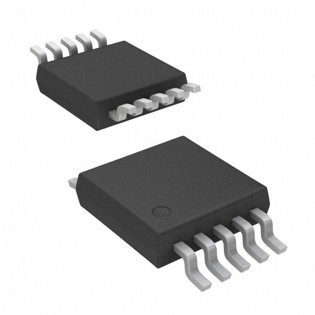
| 供应商器件封装 | 10-VSSOP |
| 其它名称 | LM5106MM/NOPBDKR |
| 包装 | Digi-Reel® |
| 商标 | Texas Instruments |
| 安装类型 | 表面贴装 |
| 安装风格 | SMD/SMT |
| 封装 | Reel |
| 封装/外壳 | 10-TFSOP,10-MSOP(0.118",3.00mm 宽) |
| 封装/箱体 | MSOP |
| 工作温度 | -40°C ~ 125°C |
| 工厂包装数量 | 1000 |
| 延迟时间 | 115ns |
| 最大工作温度 | + 125 C |
| 最小工作温度 | - 40 C |
| 标准包装 | 1 |
| 激励器数量 | 2 Driver |
| 电压-电源 | 8 V ~ 14 V |
| 电流-峰值 | 1.8A |
| 电源电压-最大 | 14 V |
| 电源电压-最小 | 8 V |
| 电源电流 | 2.1 mA (Typ) |
| 类型 | High and Low Side |
| 系列 | LM5106 |
| 输入类型 | PWM |
| 输出数 | 2 |
| 输出电流 | 1.8 A (Typ) |
| 输出端数量 | 2 |
| 配置 | Inverting, Non-Inverting |
| 配置数 | 1 |
| 高压侧电压-最大值(自举) | 118V |


- 商务部:美国ITC正式对集成电路等产品启动337调查
- 曝三星4nm工艺存在良率问题 高通将骁龙8 Gen1或转产台积电
- 太阳诱电将投资9.5亿元在常州建新厂生产MLCC 预计2023年完工
- 英特尔发布欧洲新工厂建设计划 深化IDM 2.0 战略
- 台积电先进制程称霸业界 有大客户加持明年业绩稳了
- 达到5530亿美元!SIA预计今年全球半导体销售额将创下新高
- 英特尔拟将自动驾驶子公司Mobileye上市 估值或超500亿美元
- 三星加码芯片和SET,合并消费电子和移动部门,撤换高东真等 CEO
- 三星电子宣布重大人事变动 还合并消费电子和移动部门
- 海关总署:前11个月进口集成电路产品价值2.52万亿元 增长14.8%


PDF Datasheet 数据手册内容提取
Product Sample & Technical Tools & Support & Folder Buy Documents Software Community LM5106 SNVS424D–JANUARY2006–REVISEDDECEMBER2014 LM5106 100-V Half-Bridge Gate Driver With Programmable Dead-Time 1 Features 3 Description • DrivesBothaHigh-SideandLow-SideN-Channel The LM5106 is a high-voltage gate driver designed to 1 drive both the high-side and low-side N-channel MOSFET MOSFETs in a synchronous buck or half-bridge • 1.8-APeakOutputSinkCurrent configuration. The floating high-side driver can work • 1.2-APeakOutputSourceCurrent with rail voltages up to 100 V. The single control input • BootstrapSupplyVoltageRangeupto118-VDC is compatible with TTL signal levels and a single external resistor programs the switching transition • SingleTTLCompatibleInput dead-time through tightly matched turnon delay • ProgrammableTurnonDelays(Dead-Time) circuits. The robust level shift technology operates at • EnableInputPin high speed while consuming low power and provides clean output transitions. Undervoltage lockout • FastTurnoffPropagationDelays(32nsTypical) (UVLO) disables the gate driver when either the low • Drives1000pFWith15-nsRiseand10-nsFall side or the bootstrapped high-side supply voltage is Time below the operating threshold. The LM5106 is offered • SupplyRailUndervoltageLockout in the 10-pin VSSOP or the thermally enhanced 10- pinWSONplasticpackage. • LowPowerConsumption • 10-PinWSONPackage(4mm× 4mm)and10- DeviceInformation(1) PinVSSOPPackage PARTNUMBER PACKAGE BODYSIZE(NOM) 2 Applications VSSOP(10) 3.00mm×3.00mm LM5106 WSON(10) 4.00mm×4.00mm • Solid-StateMotorDrives (1) For all available packages, see the orderable addendum at • Half-BridgeandFull-BridgePowerConverters theendofthedatasheet. • TwoSwitchForwardPowerConverters SimplifiedBlockDiagram VDD HB VDD UHVBL O LSEHVIFE TL DRIVER HO HS VDD UVLO VSS IN LEADING EDGE DELAY RDT LEEADDGINE G VDD DELAY EN DRIVER LO 1 An IMPORTANT NOTICE at the end of this data sheet addresses availability, warranty, changes, use in safety-critical applications, intellectualpropertymattersandotherimportantdisclaimers.PRODUCTIONDATA.
LM5106 SNVS424D–JANUARY2006–REVISEDDECEMBER2014 www.ti.com Table of Contents 1 Features.................................................................. 1 7.3 FeatureDescription.................................................11 2 Applications........................................................... 1 7.4 DeviceFunctionalModes........................................11 3 Description............................................................. 1 8 ApplicationandImplementation........................ 12 4 RevisionHistory..................................................... 2 8.1 ApplicationInformation............................................12 8.2 TypicalApplication .................................................12 5 PinConfigurationandFunctions......................... 3 9 PowerSupplyRecommendations...................... 14 6 Specifications......................................................... 4 9.1 PowerDissipationConsiderations..........................14 6.1 AbsoluteMaximumRatings......................................4 10 Layout................................................................... 15 6.2 ESDRatings..............................................................4 6.3 RecommendedOperatingConditions.......................4 10.1 LayoutGuidelines.................................................15 6.4 ThermalInformation..................................................5 10.2 LayoutExample....................................................16 6.5 ElectricalCharacteristics...........................................5 11 DeviceandDocumentationSupport................. 17 6.6 SwitchingCharacteristics..........................................6 11.1 Trademarks...........................................................17 6.7 TypicalCharacteristics..............................................8 11.2 ElectrostaticDischargeCaution............................17 7 DetailedDescription............................................ 11 11.3 Glossary................................................................17 7.1 Overview.................................................................11 12 Mechanical,Packaging,andOrderable Information........................................................... 17 7.2 FunctionalBlockDiagram.......................................11 4 Revision History NOTE:Pagenumbersforpreviousrevisionsmaydifferfrompagenumbersinthecurrentversion. ChangesfromRevisionC(March2013)toRevisionD Page • AddedPinConfigurationandFunctionssection,ESDRatingstable,FeatureDescriptionsection,DeviceFunctional Modes,ApplicationandImplementationsection,PowerSupplyRecommendationssection,Layoutsection,Device andDocumentationSupportsection,andMechanical,Packaging,andOrderableInformationsection .............................. 1 ChangesfromRevisionB(March2013)toRevisionC Page • ChangedlayoutofNationalDataSheettoTIformat........................................................................................................... 12 2 SubmitDocumentationFeedback Copyright©2006–2014,TexasInstrumentsIncorporated ProductFolderLinks:LM5106
LM5106 www.ti.com SNVS424D–JANUARY2006–REVISEDDECEMBER2014 5 Pin Configuration and Functions 10-Pin VSSOP(DGS),WSON(DPR) TopView VDD 1 10 LO HB 2 9 VSS HO 3 8 IN HS 4 7 EN NC 5 6 RDT PinFunctions PIN DESCRIPTION APPLICATIONINFORMATION NO. NAME 1 VDD Positivegatedrivesupply DecoupleVDDtoVSSusingalowESR/ESLcapacitor,placedascloseto theICaspossible. 2 HB High-sidegatedriver ConnectthepositiveterminalofbootstrapcapacitortotheHBpinand bootstraprail connectnegativeterminaltoHS.TheBootstrapcapacitorshouldbeplaced asclosetoICaspossible. 3 HO High-sidegatedriveroutput Connecttothegateofhigh-sideN-MOSdevicethroughashort,low inductancepath. 4 HS High-sideMOSFETsource Connecttothenegativeterminalofthebootststrapcapacitorandtothe connection sourceofthehigh-sideN-MOSdevice. 5 NC Notconnected 6 RDT Dead-timeprogrammingpin AresistorfromRDTtoVSSprogramstheturnondelayofboththehigh-and low-sideMOSFETs.TheresistorshouldbeplacedclosetotheICto minimizenoisecouplingfromadjacentPCboardtraces. 7 EN Logicinputfordriver TTLcompatiblethresholdwithhysteresis.LOandHOareheldinthelow Disable/Enable statewhenENislow. 8 IN Logicinputforgatedriver TTLcompatiblethresholdwithhysteresis.Thehigh-sideMOSFETisturned onandthelow-sideMOSFETturnedoffwhenINishigh. 9 VSS Groundreturn Allsignalsarereferencedtothisground. 10 LO Low-sidegatedriveroutput Connecttothegateofthelow-sideN-MOSdevicewithashort,low inductancepath. — EP ExposedPad Theexposedpadhasnoelectricalcontact.Connecttosystemgroundplane forreducedthermalresistance. Copyright©2006–2014,TexasInstrumentsIncorporated SubmitDocumentationFeedback 3 ProductFolderLinks:LM5106
LM5106 SNVS424D–JANUARY2006–REVISEDDECEMBER2014 www.ti.com 6 Specifications 6.1 Absolute Maximum Ratings(1)(2) MIN MAX UNIT V toV –0.3 18 V DD SS HBtoHS –0.3 18 V INandENtoV –0.3 V +0.3 V SS DD LOtoV –0.3 V +0.3 V SS DD HOtoV HS–0.3 HB+0.3 V SS HStoV (3) 100 V SS HBtoV 118 V SS RDTtoV –0.3 5 V SS JunctionTemperature 150 °C Storagetemperaturerange,T –55 150 °C stg (1) AbsoluteMaximumRatingsindicatelimitsbeyondwhichdamagetothecomponentmayoccur.RecommendedOperatingConditionsare conditionsunderwhichoperationofthedeviceisensured.OperatingRatingsdonotimplyensuredperformancelimits.Forensured performancelimitsandassociatedtestconditions,seetheElectricalCharacteristics. (2) IfMilitary/Aerospacespecifieddevicesarerequired,pleasecontacttheTexasInstrumentsSalesOffice/Distributorsforavailabilityand specifications. (3) IntheapplicationtheHSnodeisclampedbythebodydiodeoftheexternallowerN-MOSFET,thereforetheHSvoltagewillgenerally notexceed–1V.Howeverinsomeapplications,boardresistanceandinductancemayresultintheHSnodeexceedingthisstated voltagetransiently.IfnegativetransientsoccuronHS,theHSvoltagemustneverbemorenegativethanV -15V.Forexample,if DD V =10V,thenegativetransientsatHSmustnotexceed–5V. DD 6.2 ESD Ratings VALUE UNIT V Electrostaticdischarge Humanbodymodel(HBM),perANSI/ESDA/JEDECJS-001(1) ±1500 V (ESD) (1) JEDECdocumentJEP155statesthat500-VHBMallowssafemanufacturingwithastandardESDcontrolprocess. 6.3 Recommended Operating Conditions MIN MAX UNIT V 8 14 V DD HS(1) –1 100 V HB HS+8 HS+14 V HSSlewRate <50 V/ns JunctionTemperature –40 125 °C (1) IntheapplicationtheHSnodeisclampedbythebodydiodeoftheexternallowerN-MOSFET,thereforetheHSvoltagewillgenerally notexceed–1V.Howeverinsomeapplications,boardresistanceandinductancemayresultintheHSnodeexceedingthisstated voltagetransiently.IfnegativetransientsoccuronHS,theHSvoltagemustneverbemorenegativethanV -15V.Forexample,if DD V =10V,thenegativetransientsatHSmustnotexceed–5V. DD 4 SubmitDocumentationFeedback Copyright©2006–2014,TexasInstrumentsIncorporated ProductFolderLinks:LM5106
LM5106 www.ti.com SNVS424D–JANUARY2006–REVISEDDECEMBER2014 6.4 Thermal Information LM5102 THERMALMETRIC(1) DGS DPR(2) UNIT 10PINS 10PINS R Junction-to-ambientthermalresistance 165.3 37.9 θJA R Junction-to-case(top)thermalresistance 58.9 38.1 θJC(top) R Junction-to-boardthermalresistance 54.4 14.9 θJB °C/W ψ Junction-to-topcharacterizationparameter 6.2 0.4 JT ψ Junction-to-boardcharacterizationparameter 83.6 15.2 JB R Junction-to-case(bottom)thermalresistance N/A 4.4 θJC(bot) (1) Formoreinformationabouttraditionalandnewthermalmetrics,seetheICPackageThermalMetricsapplicationreport(SPRA953). (2) Four-layerboardwithCufinishedthickness1.5oz,1oz,1oz,1.5oz.Maximumdiesizeused.5xbodylengthofCutraceonPCBtop. 50-mm×50-mmgroundandpowerplanesembeddedinPCB.SeeApplicationNoteAN-1187LeadlessLeadframePackage(LLP) (SNOA401). 6.5 Electrical Characteristics MINandMAXlimitsapplyoverthefulloperatingjunctiontemperaturerange.Unlessotherwisespecified,T =+25°C,V = J DD HB=12V,V =HS=0V,EN=5V.NoloadonLOorHO.RDT=100kΩ(1). SS SYMBOL PARAMETER TESTCONDITIONS MIN TYP MAX UNIT SUPPLYCURRENTS I V QuiescentCurrent IN=EN=0V 0.34 0.6 mA DD DD I V OperatingCurrent f=500kHz 2.1 3.5 mA DDO DD I TotalHBQuiescentCurrent IN=EN=0V 0.06 0.2 mA HB I TotalHBOperatingCurrent f=500kHz 1.5 3 mA HBO I HBtoV Current,Quiescent HS=HB=100V 0.1 10 µA HBS SS I HBtoV Current,Operating f=500kHz 0.5 mA HBSO SS INPUTINandEN V LowLevelInputVoltageThreshold 0.8 1.8 V IL V HighLevelInputVoltageThreshold 1.8 2.2 V IH R InputPulldownResistancePinINandEN 100 200 500 kΩ pd DEAD-TIMECONTROLS VRDT NominalVoltageatRDT 2.7 3 3.3 V IRDT RDTPinCurrentLimit RDT=0V 0.75 1.5 2.25 mA UNDERVOLTAGEPROTECTION V V RisingThreshold 6.2 6.9 7.6 V DDR DD V V ThresholdHysteresis 0.5 V DDH DD V HBRisingThreshold 5.9 6.6 7.3 V HBR V HBThresholdHysteresis 0.4 V HBH LOGATEDRIVER V Low-LevelOutputVoltage I =100mA 0.21 0.4 V OLL LO V I =–100mA, OHL High-LevelOutputVoltage LO 0.5 0.85 V V =V –V OHL DD LO I PeakPullupCurrent LO=0V 1.2 A OHL I PeakPulldownCurrent LO=12V 1.8 A OLL HOGATEDRIVER V Low-LevelOutputVoltage I =100mA 0.21 0.4 V OLH HO V I =–100mA, OHH High-LevelOutputVoltage HO 0.5 0.85 V V =HB–HO OHH (1) MinandMaxlimitsare100%productiontestedat25°C.Limitsovertheoperatingtemperaturerangeareensuredthroughcorrelation usingStatisticalQualityControl(SQC)methods.LimitsareusedtocalculateAverageOutgoingQualityLevel(AOQL). Copyright©2006–2014,TexasInstrumentsIncorporated SubmitDocumentationFeedback 5 ProductFolderLinks:LM5106
LM5106 SNVS424D–JANUARY2006–REVISEDDECEMBER2014 www.ti.com Electrical Characteristics (continued) MINandMAXlimitsapplyoverthefulloperatingjunctiontemperaturerange.Unlessotherwisespecified,T =+25°C,V = J DD HB=12V,V =HS=0V,EN=5V.NoloadonLOorHO.RDT=100kΩ(1). SS SYMBOL PARAMETER TESTCONDITIONS MIN TYP MAX UNIT I PeakPullupCurrent HO=0V 1.2 A OHH I PeakPulldownCurrent HO=12V 1.8 A OLH THERMALRESISTANCE θ JunctiontoAmbient See(2)(3) 40 °C/W JA (2) Four-layerboardwithCufinishedthickness1.5/1.0/1.0/1.5oz.Maximumdiesizeused.5xbodylengthofCutraceonPCBtop.50-mm ×50-mmgroundandpowerplanesembeddedinPCB.SeeAN-1187LeadlessLeadframePackage(LLP),SNOA401. (3) Theθ isnotaconstantforthepackageanddependsontheprintedcircuitboarddesignandtheoperatingconditions. JA 6.6 Switching Characteristics MINandMAXlimitsapplyoverthefulloperatingjunctiontemperaturerange.Unlessotherwisespecified,T =+25°C,V = J DD HB=12V,V =HS=0V,NoLoadonLOorHO(1). SS SYMBOL PARAMETER TESTCONDITIONS MIN TYP MAX UNIT t LowerTurn-OffPropagationDelay 32 56 ns LPHL t UpperTurn-OffPropagationDelay 32 56 HPHL t LowerTurn-OnPropagationDelay RDT=100k 400 520 640 LPLH t UpperTurn-OnPropagationDelay RDT=100k 450 570 690 HPLH t LowerTurn-OnPropagationDelay RDT=10k 85 115 160 LPLH t UpperTurn-OnPropagationDelay RDT=10k 85 115 160 HPLH t ,t EnableandShutdownpropagationdelay 36 en sd DT1,DT2 Dead-timeLOOFFtoHOON&HOOFFto RDT=100k 510 LOON RDT=10k 86 MDT Dead-timematching RDT=100k 50 t EitherOutputRiseTime C =1000pF 15 R L t EitherOutputFallTime C =1000pF 10 F L (1) MinandMaxlimitsare100%productiontestedat25°C.Limitsovertheoperatingtemperaturerangeareensuredthroughcorrelation usingStatisticalQualityControl(SQC)methods.LimitsareusedtocalculateAverageOutgoingQualityLevel(AOQL). IN EN tLPHL tHPHL tHPLH tLPLH LO ten DT1 DT2 DT1 DT2 tsd H O ten tsd Figure1. LM5106Input-OutputWaveforms 6 SubmitDocumentationFeedback Copyright©2006–2014,TexasInstrumentsIncorporated ProductFolderLinks:LM5106
LM5106 www.ti.com SNVS424D–JANUARY2006–REVISEDDECEMBER2014 IN VIH VIL tLPHL tLPLH 90% LO 10% tHPLH tHPHL 90% HO 10% Figure2. LM5106SwitchingTimeDefinitions:t ,t ,t ,t LPLH LPHL HPLH HPHL 90% HO 10% DT1 DT2 90% MDT = |DT1-DT2| LO 10% Figure3. LM5106Dead-time:DT Copyright©2006–2014,TexasInstrumentsIncorporated SubmitDocumentationFeedback 7 ProductFolderLinks:LM5106
LM5106 SNVS424D–JANUARY2006–REVISEDDECEMBER2014 www.ti.com 6.7 Typical Characteristics 100 2.2 VDD = HB = 12V VDD = HB = 12V CL = 2200 pF 2.0 VSS = HS = 0V VSS = HS = 0 RDT = 10K f = 500 kHz CL = 1000 pF )A )A 1.8 CL = 0 pF m m IDDO ( T CL = 470 pF ( T N 10 N 1.6 E E R R R R U U C C 1.4 IHBO 1.2 CL = 0 pF 1 1.0 1 10 100 1000 -50 -30 -10 10 30 50 70 90 110130150 FREQUENCY (kHz) TEMPERATURE (oC) Figure4.V OperatingCurrentvsFrequency Figure5.OperatingCurrentvsTemperature DD 1.20 1.20 IDD @ RDT = 10k 1.00 1.00 IDD @ RDT = 10k )Am 0.80 VDD = HB )Am 0.80 VDD = HB = 12V ( T VSS = HS = 0V ( T VSS = HS = 0V N 0.60 N 0.60 E E R R R IDD @ RDT = 100k R IDD @ RDT = 100k U U C 0.40 C 0.40 0.20 IHB @ RDT = 10k, 100k 0.20 IHB @ RDT = 10k, 100k 0.00 0.00 8 9 10 11 12 13 14 15 16 17 18 -50 -25 0 25 50 75 100 125 150 VDD, VHB (V) TEMPERATURE (°C) Figure7.QuiescentCurrentvsTemperature Figure6.QuiescentCurrentvsSupplyVoltage 100000 1.40 2.00 HB = 12V, CL = 4400 pF 1.26 VDD = HB = 12V, HS = 0V 1.80 HS = 0V CL = 2200 pF 1.12 1.60 )A( TP 10000 CL = 1000 pF )A( TNER 00..8948 SOURCING 11..2400 A)( TN NERRUC 1100000 RUC ECRUO 000...457260 SINKING 001...680000 ERRUC KNIS S 0.28 0.40 CL = 0 pF 0.14 0.20 CL = 470 pF 10 0.00 0.00 0.1 1 10 100 1000 0 2 4 6 8 10 12 HO, LO (V) FREQUENCY (kHz) Figure8.HBOperatingCurrentvsFrequency Figure9.HOandLOPeakOutputCurrentvsOutputVoltage 8 SubmitDocumentationFeedback Copyright©2006–2014,TexasInstrumentsIncorporated ProductFolderLinks:LM5106
LM5106 www.ti.com SNVS424D–JANUARY2006–REVISEDDECEMBER2014 Typical Characteristics (continued) 0.60 7.30 7.20 VDDR = VDD - VSS VHBR = HB - HS 0.55 7.10 VDDH 7.00 0.50 )V( D 6.90 VDDR S (V) LO ESI 0.45 HS 6.80 TER VHBH ERH 6.70 VHBR HYS 0.40 T 6.60 6.50 0.35 6.40 0.30 6.30 -50 -25 0 25 50 75 100 125 150 -50 -25 0 25 50 75 100 125 150 TEMPERATURE (°C) TEMPERATURE (oC) Figure11.UndervoltageHysteresisvsTemperature Figure10.UndervoltageRisingThresholdvsTemperature 0.400 1.300 Output Current - 100 mA Output Current = 100 mA 0.350 1.100 VDD = HB = 8V VDD = HB = 8V 0.300 0.900 )V VDD = HB = 12V )V VDD = HB = 12V ( L 0.250 ( H 0.700 O O V V 0.200 0.500 VDD = HB = 16V VDD = HB = 16V 0.150 0.300 0.100 0.100 -50 -25 0 25 50 75 100 125 150 -50 -25 0 25 50 75 100 125 150 TEMPERATURE (°C) TEMPERATURE (°C) Figure12.LOandHO-Low-LevelOutputVoltagevs Figure13.LOandHO-High-LevelOutputVoltagevs Temperature Temperature 1.96 88 1.94 86 1.92 VDD = HB = 12V 1.90 VSS = HS = 0 )s 84 V (V)IH 11..8868 n( EMIT 82 V, IL 1.84 -DA 1.82 ED 80 1.80 78 1.78 1.76 76 -50 -30 -10 10 30 50 70 90 110 130 150 -50 -30 -10 10 30 50 70 90 110130150 TEMPERATURE (oC) TEMPERATURE (oC) Figure15.Dead-TimevsTemperature(RT=10k) Figure14.InputThresholdvsTemperature Copyright©2006–2014,TexasInstrumentsIncorporated SubmitDocumentationFeedback 9 ProductFolderLinks:LM5106
LM5106 SNVS424D–JANUARY2006–REVISEDDECEMBER2014 www.ti.com Typical Characteristics (continued) 600 590 VDD = HB = 12V VSS = HS = 0V )s 580 n ( E M IT 570 -D A ED 560 550 540 -50 -30 -10 10 30 50 70 90 110130150 TEMPERATURE (oC) Figure16.Dead-TimevsTemperature(RT=100k) 10 SubmitDocumentationFeedback Copyright©2006–2014,TexasInstrumentsIncorporated ProductFolderLinks:LM5106
LM5106 www.ti.com SNVS424D–JANUARY2006–REVISEDDECEMBER2014 7 Detailed Description 7.1 Overview TheLM5106isasinglePWMinputgatedriverwithEnablethatoffersaprogrammabledead-time.Thedead-time is set with a resistor at the RDT pin and can be adjusted from 100 ns to 600 ns. The wide dead-time programming range provides the flexibility to optimize drive signal timing for a wide range of MOSFETs and applications. The RDT pin is biased at 3 V and current limited to 1 mA maximum programming current. The time delay generator will accommodate resistor values from 5k to 100k with a dead-time time that is proportional to the RDT resistance.GroundingtheRDTpinprogramstheLM5106todrivebothoutputswithminimumdead-time. 7.2 Functional Block Diagram VDD HB VDD UHVBL O LSEHVIFE TL DRIVER HO HS VDD UVLO VSS IN LEADING EDGE DELAY RDT LEEADDGINE G VDD DELAY EN DRIVER LO 7.3 Feature Description 7.3.1 Start-upandUVLO Both top and bottom drivers include undervoltage lockout (UVLO) protection circuitry which monitors the supply voltage (V ) and bootstrap capacitor voltage (HB – HS) independently. The UVLO circuit inhibits each driver DD until sufficient supply voltage is available to turn on the external MOSFETs, and the UVLO hysteresis prevents chatteringduringsupplyvoltagetransitions.WhenthesupplyvoltageisappliedtotheV pinoftheLM5106,the DD top and bottom gates are held low until V exceeds the UVLO threshold, typically about 6.9 V. Any UVLO DD conditiononthebootstrapcapacitorwilldisableonlythehigh-sideoutput(HO). 7.4 Device Functional Modes EN INPin LOPin HOPin L Any L L H H L H H L H L Copyright©2006–2014,TexasInstrumentsIncorporated SubmitDocumentationFeedback 11 ProductFolderLinks:LM5106
LM5106 SNVS424D–JANUARY2006–REVISEDDECEMBER2014 www.ti.com 8 Application and Implementation NOTE Information in the following applications sections is not part of the TI component specification, and TI does not warrant its accuracy or completeness. TI’s customers are responsible for determining suitability of components for their purposes. Customers should validateandtesttheirdesignimplementationtoconfirmsystemfunctionality. 8.1 Application Information The LM5106 is one of the latest generation of high-voltage gate drivers which are designed to drive both the high-side and low-side N-channel MOSFETs in a half-bridge/full bridge configuration or in a synchronous buck circuit. The floating high-side driver can operate with supply voltages up to 110 V. This allows for N-channel MOSFETcontrolinhalf-bridge,full-bridge,push-pull,twoswitchforwardandactiveclamptopologies. TheoutputsoftheLM5106arecontrolledfromasingleinput.Therisingedgeofeachoutputcanbedelayedwith aprogrammingresistor. Table1.Highlights FEATURE BENEFIT ProgrammableTurnonDelay Allowsoptimizationofgatedrivetimingsinbridgetopologies Reducesoperatingcurrentwhendisabledtoimprovedpowersystem EnablePin standbypower LowPowerConsumption Improveslightloadefficiencyfiguresofthepowerstage. 8.2 Typical Application VIN VCC HB RGATE VDD VDD HO CBOOT 0.1 PF OUT1 IN HS CONTROLLER LM5106 T1 ENABLE EN LO 0.47 PF RDT RGATE GND VSS Figure17. LM5106DrivingMOSFETsConnectedinHalf-BridgeConfiguration 12 SubmitDocumentationFeedback Copyright©2006–2014,TexasInstrumentsIncorporated ProductFolderLinks:LM5106
LM5106 www.ti.com SNVS424D–JANUARY2006–REVISEDDECEMBER2014 Typical Application (continued) 8.2.1 DesignRequirements PARAMETERS VALUES GateDriveIC LM5102 Mosfet CSD18531Q5A V 10V DD Q 43nC gmax F 100kHz sw D 95% Max I 10µA HBO V 1.1V DH V 7.3V HBR V 0.4V HBH 8.2.2 DetailedDesignProcedure 8.2.2.1 DetailedDesignProcedure ΔV =V –V –V HB DD DH HBL where • V =SupplyvoltageofthegatedriveIC DD • V =Bootstrapdiodeforwardvoltagedrop DH • V =Minimumgatesourcethresholdvoltage (1) gsmin Q C = TOTAL BOOT DVHB (2) D Q =Q +I ´ Max TOTAL gmax HBO FSW (3) Thequiescentcurrentofthebootstrapcircuitis10 µAwhichisnegligiblecomparedtotheQgsoftheMOSFET. 0.95 QTOTAL =43nC+10mA´ 100kHz (4) Q =43.01nC (5) TOTAL In practice the value for the C capacitor should be greater than that calculated to allow for situations where BOOT the power stage may skip pulse due to load transients. In this circumstance the boot capacitor must maintain the HBpinvoltageabovetheUVLOvoltagefortheHBcircuit. AsageneralrulethelocalV bypasscapacitorshouldbe10timesgreaterthanthevalueofC . DD BOOT V =V –V (6) HBL HBR HBH V =6.9V (7) HBL ΔV =10V–1.1V–6.9V (8) HB ΔV =2.0V (9) HB C =43.01nc/2V (10) BOOT C =21.5nF (11) BOOT The bootstrap and bias capacitors should be ceramic types with X7R dielectric. The voltage rating should be twice that of the maximum VDD to allow for loss of capacitance once the devices have a DC bias voltage across themandtoensurelong-termreliabilityofthedevices. Theresistorvalues,RT,forsettingturnondelaycanbefoundinFigure19. Copyright©2006–2014,TexasInstrumentsIncorporated SubmitDocumentationFeedback 13 ProductFolderLinks:LM5106
LM5106 SNVS424D–JANUARY2006–REVISEDDECEMBER2014 www.ti.com 8.2.3 ApplicationCurves EN VIH 90% LO or HO tsd Figure18. LM5106Enable:t sd 900 800 700 )s 600 n ( EM 500 IT -D 400 A E D 300 200 100 0 10 30 50 70 90 110 130 150 RDT (k:) Figure19. Dead-TimevsRTResistorValue 9 Power Supply Recommendations 9.1 Power Dissipation Considerations The total IC power dissipation is the sum of the gate driver losses and the bootstrap diode losses. The gate driver losses are related to the switching frequency (f), output load capacitance on LO and HO (C ), and supply L voltage(V )andcanberoughlycalculatedas: DD P =2•f•C •V 2 (12) DGATES L DD There are some additional losses in the gate drivers due to the internal CMOS stages used to buffer the LO and HO outputs. Figure 20 shows the measured gate driver power dissipation versus frequency and load capacitance. At higher frequencies and load capacitance values, the power dissipation is dominated by the power losses driving the output loads and agrees well with the Equation 12. This plot can be used to approximatethepowerlossesduetothegatedrivers. 14 SubmitDocumentationFeedback Copyright©2006–2014,TexasInstrumentsIncorporated ProductFolderLinks:LM5106
LM5106 www.ti.com SNVS424D–JANUARY2006–REVISEDDECEMBER2014 Power Dissipation Considerations (continued) 1.000 CL = 4400 pF CL = 2200 pF 0.100 W) R ( CL = 1000 pF E W O P 0.010 CL = 470 pF CL = 0 pF 0.001 0.1 1.0 10.0 100.0 1000.0 SWITCHING FREQUENCY (kHz) Figure20. GateDriverPowerDissipation(LO+HO) V =12V CC 10 Layout 10.1 Layout Guidelines The optimum performance of high- and low-side gate drivers cannot be achieved without taking due considerationsduringcircuitboardlayout.Thefollowingpointsareemphasized: 1. Low ESR / ESL capacitors must be connected close to the IC between VDD and VSS pins and between HB and HS pins to support high peak currents being drawn from VDD and HB during the turnon of the external MOSFETs. 2. To prevent large voltage transients at the drain of the top MOSFET, a low ESR electrolytic capacitor and a goodqualityceramiccapacitormustbeconnectedbetweentheMOSFETdrainandground(VSS). 3. Toavoidlargenegativetransientsontheswitchnode(HS)pin,theparasiticinductancesbetweenthesource ofthetopMOSFETandthedrainofthebottomMOSFET(synchronousrectifier)mustbeminimized. 4. Groundingconsiderations: – The first priority in designing grounding connections is to confine the high peak currents that charge and discharge the MOSFET gates to a minimal physical area. This will decrease the loop inductance and minimize noise issues on the gate terminals of the MOSFETs. The gate driver should be placed as close aspossibletotheMOSFETs. – The second consideration is the high current path that includes the bootstrap capacitor, the bootstrap diode, the local ground referenced bypass capacitor, and the low-side MOSFET body diode. The bootstrap capacitor is recharged on a cycle-by-cycle basis through the bootstrap diode from the ground referenced VDD bypass capacitor. The recharging occurs in a short time interval and involves high peak current.Minimizingthislooplengthandareaonthecircuitboardisimportanttoensurereliableoperation. 5. The resistor on the RDT pin must be placed very close to the IC and separated from the high current paths toavoidnoisecouplingtothetimedelaygeneratorwhichcoulddisrupttimeroperation. 10.1.1 HSTransientVoltagesBelowGround The HS node will always be clamped by the body diode of the lower external FET. In some situations, board resistances and inductances can cause the HS node to transiently swing several volts below ground. The HS nodecanswingbelowgroundprovided: 1. HS must always be at a lower potential than HO. Pulling HO more than –0.3 V below HS can activate parasitic transistors resulting in excessive current flow from the HB supply, possibly resulting in damage to the IC. The same relationship is true with LO and VSS. If necessary, a Schottky diode can be placed Copyright©2006–2014,TexasInstrumentsIncorporated SubmitDocumentationFeedback 15 ProductFolderLinks:LM5106
LM5106 SNVS424D–JANUARY2006–REVISEDDECEMBER2014 www.ti.com Layout Guidelines (continued) externally between HO and HS or LO and GND to protect the IC from this type of transient. The diode must beplacedasclosetotheICpinsaspossibleinordertobeeffective. 2. HB to HS operating voltage should be 15 V or less. Hence, if the HS pin transient voltage is –5 V, VDD shouldbeideallylimitedto10VtokeepHBtoHSbelow15V. 3. Low ESR bypass capacitors from HB to HS and from VCC to VSS are essential for proper operation. The capacitor should be located at the leads of the IC to minimize series inductance. The peak currents from LO and HO can be quite large. Any inductances in series with the bypass capacitor will cause voltage ringing at theleadsoftheICwhichmustbeavoidedforreliableoperation. 10.2 Layout Example C BOOT Q HS C V DD LM5106 Q LS Figure21. LM5106ComponentPlacement 16 SubmitDocumentationFeedback Copyright©2006–2014,TexasInstrumentsIncorporated ProductFolderLinks:LM5106
LM5106 www.ti.com SNVS424D–JANUARY2006–REVISEDDECEMBER2014 11 Device and Documentation Support 11.1 Trademarks Alltrademarksarethepropertyoftheirrespectiveowners. 11.2 Electrostatic Discharge Caution Thesedeviceshavelimitedbuilt-inESDprotection.Theleadsshouldbeshortedtogetherorthedeviceplacedinconductivefoam duringstorageorhandlingtopreventelectrostaticdamagetotheMOSgates. 11.3 Glossary SLYZ022—TIGlossary. Thisglossarylistsandexplainsterms,acronyms,anddefinitions. 12 Mechanical, Packaging, and Orderable Information The following pages include mechanical, packaging, and orderable information. This information is the most current data available for the designated devices. This data is subject to change without notice and revision of thisdocument.Forbrowser-basedversionsofthisdatasheet,refertotheleft-handnavigation. Copyright©2006–2014,TexasInstrumentsIncorporated SubmitDocumentationFeedback 17 ProductFolderLinks:LM5106
PACKAGE OPTION ADDENDUM www.ti.com 29-Nov-2017 PACKAGING INFORMATION Orderable Device Status Package Type Package Pins Package Eco Plan Lead/Ball Finish MSL Peak Temp Op Temp (°C) Device Marking Samples (1) Drawing Qty (2) (6) (3) (4/5) LM5106MM/NOPB ACTIVE VSSOP DGS 10 1000 Green (RoHS CU SN Level-1-260C-UNLIM -40 to 125 5106 & no Sb/Br) LM5106MMX/NOPB ACTIVE VSSOP DGS 10 3500 Green (RoHS CU SN Level-1-260C-UNLIM -40 to 125 5106 & no Sb/Br) LM5106SD/NOPB ACTIVE WSON DPR 10 1000 Green (RoHS CU NIPDAU | CU SN Level-1-260C-UNLIM -40 to 125 L5106SD & no Sb/Br) LM5106SDX/NOPB ACTIVE WSON DPR 10 4500 Green (RoHS CU NIPDAU | CU SN Level-1-260C-UNLIM -40 to 125 L5106SD & no Sb/Br) (1) The marketing status values are defined as follows: ACTIVE: Product device recommended for new designs. LIFEBUY: TI has announced that the device will be discontinued, and a lifetime-buy period is in effect. NRND: Not recommended for new designs. Device is in production to support existing customers, but TI does not recommend using this part in a new design. PREVIEW: Device has been announced but is not in production. Samples may or may not be available. OBSOLETE: TI has discontinued the production of the device. (2) RoHS: TI defines "RoHS" to mean semiconductor products that are compliant with the current EU RoHS requirements for all 10 RoHS substances, including the requirement that RoHS substance do not exceed 0.1% by weight in homogeneous materials. Where designed to be soldered at high temperatures, "RoHS" products are suitable for use in specified lead-free processes. TI may reference these types of products as "Pb-Free". RoHS Exempt: TI defines "RoHS Exempt" to mean products that contain lead but are compliant with EU RoHS pursuant to a specific EU RoHS exemption. Green: TI defines "Green" to mean the content of Chlorine (Cl) and Bromine (Br) based flame retardants meet JS709B low halogen requirements of <=1000ppm threshold. Antimony trioxide based flame retardants must also meet the <=1000ppm threshold requirement. (3) MSL, Peak Temp. - The Moisture Sensitivity Level rating according to the JEDEC industry standard classifications, and peak solder temperature. (4) There may be additional marking, which relates to the logo, the lot trace code information, or the environmental category on the device. (5) Multiple Device Markings will be inside parentheses. Only one Device Marking contained in parentheses and separated by a "~" will appear on a device. If a line is indented then it is a continuation of the previous line and the two combined represent the entire Device Marking for that device. (6) Lead/Ball Finish - Orderable Devices may have multiple material finish options. Finish options are separated by a vertical ruled line. Lead/Ball Finish values may wrap to two lines if the finish value exceeds the maximum column width. Important Information and Disclaimer:The information provided on this page represents TI's knowledge and belief as of the date that it is provided. TI bases its knowledge and belief on information provided by third parties, and makes no representation or warranty as to the accuracy of such information. Efforts are underway to better integrate information from third parties. TI has taken and Addendum-Page 1
PACKAGE OPTION ADDENDUM www.ti.com 29-Nov-2017 continues to take reasonable steps to provide representative and accurate information but may not have conducted destructive testing or chemical analysis on incoming materials and chemicals. TI and TI suppliers consider certain information to be proprietary, and thus CAS numbers and other limited information may not be available for release. In no event shall TI's liability arising out of such information exceed the total purchase price of the TI part(s) at issue in this document sold by TI to Customer on an annual basis. Addendum-Page 2
PACKAGE MATERIALS INFORMATION www.ti.com 28-Apr-2019 TAPE AND REEL INFORMATION *Alldimensionsarenominal Device Package Package Pins SPQ Reel Reel A0 B0 K0 P1 W Pin1 Type Drawing Diameter Width (mm) (mm) (mm) (mm) (mm) Quadrant (mm) W1(mm) LM5106MM/NOPB VSSOP DGS 10 1000 178.0 12.4 5.3 3.4 1.4 8.0 12.0 Q1 LM5106MMX/NOPB VSSOP DGS 10 3500 330.0 12.4 5.3 3.4 1.4 8.0 12.0 Q1 LM5106SD/NOPB WSON DPR 10 1000 180.0 12.4 4.3 4.3 1.1 8.0 12.0 Q1 LM5106SDX/NOPB WSON DPR 10 4500 330.0 12.4 4.3 4.3 1.3 8.0 12.0 Q1 PackMaterials-Page1
PACKAGE MATERIALS INFORMATION www.ti.com 28-Apr-2019 *Alldimensionsarenominal Device PackageType PackageDrawing Pins SPQ Length(mm) Width(mm) Height(mm) LM5106MM/NOPB VSSOP DGS 10 1000 210.0 185.0 35.0 LM5106MMX/NOPB VSSOP DGS 10 3500 367.0 367.0 35.0 LM5106SD/NOPB WSON DPR 10 1000 203.0 203.0 35.0 LM5106SDX/NOPB WSON DPR 10 4500 367.0 367.0 35.0 PackMaterials-Page2
PACKAGE OUTLINE DGS0010A VSSOP - 1.1 mm max height SCALE 3.200 SMALL OUTLINE PACKAGE C 5.05 4.75 TYP SEATING PLANE A PIN 1 ID 0.1 C AREA 8X 0.5 10 1 3.1 2X 2.9 NOTE 3 2 5 6 0.27 10X 0.17 B 3.1 0.1 C A B 1.1 MAX 2.9 NOTE 4 0.23 TYP SEE DETAIL A 0.13 0.25 GAGE PLANE 0.15 0.7 0 - 8 0.05 0.4 DETAIL A TYPICAL 4221984/A 05/2015 NOTES: 1. All linear dimensions are in millimeters. Any dimensions in parenthesis are for reference only. Dimensioning and tolerancing per ASME Y14.5M. 2. This drawing is subject to change without notice. 3. This dimension does not include mold flash, protrusions, or gate burrs. Mold flash, protrusions, or gate burrs shall not exceed 0.15 mm per side. 4. This dimension does not include interlead flash. Interlead flash shall not exceed 0.25 mm per side. 5. Reference JEDEC registration MO-187, variation BA. www.ti.com
EXAMPLE BOARD LAYOUT DGS0010A VSSOP - 1.1 mm max height SMALL OUTLINE PACKAGE 10X (1.45) 10X (0.3) SYMM (R0.05) TYP 1 10 SYMM 8X (0.5) 5 6 (4.4) LAND PATTERN EXAMPLE SCALE:10X SOOPLEDNEINRG MASK METAL MSOELTDAEL RU NMDAESRK SOOPLEDNEINRG MASK 0.05 MAX 0.05 MIN ALL AROUND ALL AROUND NON SOLDER MASK SOLDER MASK DEFINED DEFINED SOLDER MASK DETAILS NOT TO SCALE 4221984/A 05/2015 NOTES: (continued) 6. Publication IPC-7351 may have alternate designs. 7. Solder mask tolerances between and around signal pads can vary based on board fabrication site. www.ti.com
EXAMPLE STENCIL DESIGN DGS0010A VSSOP - 1.1 mm max height SMALL OUTLINE PACKAGE 10X (1.45) SYMM (R0.05) TYP 10X (0.3) 1 10 SYMM 8X (0.5) 5 6 (4.4) SOLDER PASTE EXAMPLE BASED ON 0.125 mm THICK STENCIL SCALE:10X 4221984/A 05/2015 NOTES: (continued) 8. Laser cutting apertures with trapezoidal walls and rounded corners may offer better paste release. IPC-7525 may have alternate design recommendations. 9. Board assembly site may have different recommendations for stencil design. www.ti.com
None
None
MECHANICAL DATA DPR0010A SDC10A (Rev A) www.ti.com
IMPORTANTNOTICEANDDISCLAIMER TIPROVIDESTECHNICALANDRELIABILITYDATA(INCLUDINGDATASHEETS),DESIGNRESOURCES(INCLUDINGREFERENCE DESIGNS),APPLICATIONOROTHERDESIGNADVICE,WEBTOOLS,SAFETYINFORMATION,ANDOTHERRESOURCES“ASIS” ANDWITHALLFAULTS,ANDDISCLAIMSALLWARRANTIES,EXPRESSANDIMPLIED,INCLUDINGWITHOUTLIMITATIONANY IMPLIEDWARRANTIESOFMERCHANTABILITY,FITNESSFORAPARTICULARPURPOSEORNON-INFRINGEMENTOFTHIRD PARTYINTELLECTUALPROPERTYRIGHTS. TheseresourcesareintendedforskilleddevelopersdesigningwithTIproducts.Youaresolelyresponsiblefor(1)selectingtheappropriate TIproductsforyourapplication,(2)designing,validatingandtestingyourapplication,and(3)ensuringyourapplicationmeetsapplicable standards,andanyothersafety,security,orotherrequirements.Theseresourcesaresubjecttochangewithoutnotice.TIgrantsyou permissiontousetheseresourcesonlyfordevelopmentofanapplicationthatusestheTIproductsdescribedintheresource.Other reproductionanddisplayoftheseresourcesisprohibited.NolicenseisgrantedtoanyotherTIintellectualpropertyrightortoanythird partyintellectualpropertyright.TIdisclaimsresponsibilityfor,andyouwillfullyindemnifyTIanditsrepresentativesagainst,anyclaims, damages,costs,losses,andliabilitiesarisingoutofyouruseoftheseresources. TI’sproductsareprovidedsubjecttoTI’sTermsofSale(www.ti.com/legal/termsofsale.html)orotherapplicabletermsavailableeitheron ti.comorprovidedinconjunctionwithsuchTIproducts.TI’sprovisionoftheseresourcesdoesnotexpandorotherwisealterTI’sapplicable warrantiesorwarrantydisclaimersforTIproducts. MailingAddress:TexasInstruments,PostOfficeBox655303,Dallas,Texas75265 Copyright©2019,TexasInstrumentsIncorporated