ICGOO在线商城 > 开发板,套件,编程器 > 评估板 - 音频放大器 > LM48822TLEVAL
 Datasheet下载
- 型号: LM48822TLEVAL
- 制造商: Texas Instruments
- 库位|库存: xxxx|xxxx
- 要求:
| 数量阶梯 | 香港交货 | 国内含税 |
| +xxxx | $xxxx | ¥xxxx |
查看当月历史价格
查看今年历史价格
LM48822TLEVAL产品简介:
ICGOO电子元器件商城为您提供LM48822TLEVAL由Texas Instruments设计生产,在icgoo商城现货销售,并且可以通过原厂、代理商等渠道进行代购。 LM48822TLEVAL价格参考。Texas InstrumentsLM48822TLEVAL封装/规格:评估板 - 音频放大器, LM48822 Boomer® Headphones, 2-Channel (Stereo) Output Class AB Audio Amplifier Evaluation Board。您可以下载LM48822TLEVAL参考资料、Datasheet数据手册功能说明书,资料中有LM48822TLEVAL 详细功能的应用电路图电压和使用方法及教程。
LM48822TLEVAL 是德州仪器(Texas Instruments)推出的一款音频功率放大器评估板,主要用于评估 LM48822 音频放大器芯片的性能。该芯片是一款高效的立体声 D 类音频放大器,适用于需要高质量音频输出和高效率的应用场景。

其主要应用场景包括:

1. 便携式音频设备:如便携式音箱、蓝牙音箱、MP3播放器等,因其高效率和低功耗特性,适合电池供电设备。

2. 智能手机与平板电脑:作为内置音频放大器,提供清晰、强劲的音频输出,支持耳机或内置扬声器驱动。

3. 汽车音响系统:适用于车载娱乐系统中,提供高保真音频放大,同时减少发热和功耗。

4. 家用音响系统:如迷你音响、智能音箱等,可用于提升音质表现并简化电源设计。

5. 评估与开发:工程师可使用该评估板快速测试 LM48822 的性能,包括输出功率、频率响应、失真度等,以加速产品开发流程。

该评估板集成了完整的音频放大电路,包含电源管理、输入接口、滤波器和输出端保护电路,便于用户进行功能验证和性能测试。
| 参数 | 数值 |
| 产品目录 | 编程器,开发系统嵌入式解决方案 |
| 描述 | BOARD EVAL FOR LM48822TL音频 IC 开发工具 LM48822TL EVAL KIT |
| 产品分类 | |
| 品牌 | Texas Instruments |
| 产品手册 | http://www.ti.com/litv/SNAS456B |
| 产品图片 |
|
| rohs | 否含铅 / 不符合限制有害物质指令(RoHS)规范要求 |
| 产品系列 | 模拟与数字IC开发工具,音频 IC 开发工具,Texas Instruments LM48822TLEVALBoomer® |
| 数据手册 | |
| 产品型号 | LM48822TLEVAL |
| 不同负载时的最大输出功率x通道数 | 40mW x 2 @ 32 欧姆 |
| 产品 | Evaluation Boards |
| 产品种类 | 音频 IC 开发工具 |
| 使用的IC/零件 | LM48822 |
| 制造商产品页 | http://www.ti.com/general/docs/suppproductinfo.tsp?distId=10&orderablePartNumber=LM48822TLEVAL |
| 商标 | Texas Instruments |
| 工作温度 | -40°C ~ 85°C |
| 工作电源电压 | 2.4 V to 5.5 V |
| 工具用于评估 | LM48822 |
| 工厂包装数量 | 1 |
| 所含物品 | 板 |
| 接口类型 | I2C |
| 描述/功能 | LM48822TLEVAL is an evaluation kit designed to ease the evaluation and effort during the development of a circuit using the LM48822TL |
| 放大器类型 | AB 类 |
| 板类型 | 完全填充 |
| 标准包装 | 1 |
| 电压-电源 | 2.4 V ~ 5.5 V |
| 相关产品 | /product-detail/zh/LM48822TL%2FNOPB/LM48822TL%2FNOPBTR-ND/1871696/product-detail/zh/LM48822TLX%2FNOPB/LM48822TLX%2FNOPB-ND/1871695 |
| 类型 | Audio Amplifiers |
| 输出类型 | 耳机,2-通道(立体声) |


- 商务部:美国ITC正式对集成电路等产品启动337调查
- 曝三星4nm工艺存在良率问题 高通将骁龙8 Gen1或转产台积电
- 太阳诱电将投资9.5亿元在常州建新厂生产MLCC 预计2023年完工
- 英特尔发布欧洲新工厂建设计划 深化IDM 2.0 战略
- 台积电先进制程称霸业界 有大客户加持明年业绩稳了
- 达到5530亿美元!SIA预计今年全球半导体销售额将创下新高
- 英特尔拟将自动驾驶子公司Mobileye上市 估值或超500亿美元
- 三星加码芯片和SET,合并消费电子和移动部门,撤换高东真等 CEO
- 三星电子宣布重大人事变动 还合并消费电子和移动部门
- 海关总署:前11个月进口集成电路产品价值2.52万亿元 增长14.8%


PDF Datasheet 数据手册内容提取
LM48822, LM48822TLEVAL www.ti.com SNAS456C–MAY2008–REVISEDMAY2013 LM48822 Boomer ™ Ground-Referenced, Ultra High PSRR, Ultra Low Noise, 2 35mW/Channel Stereo Headphone Amplifier with Common Mode Sense, and I C Volume Control CheckforSamples:LM48822,LM48822TLEVAL FEATURES DESCRIPTION 1 • GroundReferencedOutputs–Eliminates The LM48822 is a single supply, ground-referenced 23 stereo headphone amplifier designed for portable OutputCouplingCapacitors devices, such as cell phones, where board space is • Common-ModeSense at a premium. The LM48822 features TI’s ground- • Ultra-HighPSRR referenced architecture, which eliminates the large • I2CVolumeandModeControl DC blocking capacitor required by traditional headphone amplifiers, saving board space and • HighOutputImpedanceinShutdown minimizingsystemcost. • DifferentialInputs The LM48822 features common-mode sensing that • AdvancedClick-and-PopSuppression corrects for any differences between the amplifier • LowSupplyCurrent ground and the potential at the headphone return • MinimumExternalComponents terminal, minimizing noise created by any ground mismatches. • Micro-PowerShutdown The LM48822 delivers 35mW/channel into a 16Ω • AvailableinSpace-Saving16-BumpDSBGA load with <1% THD+N with a 3.6V supply. High Package power supply rejection ratio (PSRR), of 110dB at 217Hz, allows the device to operate in noisy APPLICATIONS environments without additional power supply • MobilePhones conditioning. Flexible power supply requirements allow operation from 2.4V to 5.5V. The LM48822 has • PDAs a differential inputs for improved noise rejection. High • NotebookPCs output impedance in Shutdown mode, combined with • PortableElectronicDevices a charge pump-only mode allows the LM48822's outputs to be driven by an external source without • MP3Players degrading the source signal. Additionally, the LM48822 features a 64-step I2C volume control and KEY SPECIFICATIONS mute function. The low power Shutdown mode • OutputPower/ChannelatV =3.6V reducessupplycurrentconsumptionto0.06µA. DD – RL=16Ω,THD+N ≤ 1%:35mW(typ) Superiorclickandpopsuppressioneliminatesaudible • OutputPower/ChannelatV =3.6V transients on power-up/down and during shutdown. DD The LM48822 is available in an ultra-small 16-bump – R =32Ω,THD+N ≤ 1%:40mW(typ) L DSBGApackage(2mmx2mm). • QuiescentPowerSupplyCurrentat3.6V: 3.5mA(typ) • PSRRat217Hz:110dB(typ) • ShutdownCurrent:0.06μA(typ) 1 Pleasebeawarethatanimportantnoticeconcerningavailability,standardwarranty,anduseincriticalapplicationsof TexasInstrumentssemiconductorproductsanddisclaimerstheretoappearsattheendofthisdatasheet. isatrademarkof~TexasInstruments. 2 Allothertrademarksarethepropertyoftheirrespectiveowners. 3 PRODUCTIONDATAinformationiscurrentasofpublicationdate. Copyright©2008–2013,TexasInstrumentsIncorporated Products conform to specifications per the terms of the Texas Instruments standard warranty. Production processing does not necessarilyincludetestingofallparameters.
LM48822, LM48822TLEVAL SNAS456C–MAY2008–REVISEDMAY2013 www.ti.com Typical Application +2.4V to +5.5V CS VDD BIAS BIASING CBIAS CIN INL+ VOLUME OUTL CONTROL AND INL- MIXER CIN SDA I2C SCL INTERFACE COM CIN INR+ VOLUME OUTR CONTROL AND INR- MIXER CIN CHARGE PUMP C1P C1N CPVSS CPGND GND C2 C1 Figure1. TypicalAudioAmplifierApplicationCircuit 2 SubmitDocumentationFeedback Copyright©2008–2013,TexasInstrumentsIncorporated ProductFolderLinks:LM48822 LM48822TLEVAL
LM48822, LM48822TLEVAL www.ti.com SNAS456C–MAY2008–REVISEDMAY2013 Connection Diagram TopView 4 VDD INL- INR- COM 3 CPGND INL+ INR+ SDA 2 C1P CPVSS GND SCL 1 C1N OUTL BIAS OUTR A B C D Figure2. DSBGAPackage 2mmx2mmx0.8mm SeePackageNumberYZR001611A Thesedeviceshavelimitedbuilt-inESDprotection.Theleadsshouldbeshortedtogetherorthedeviceplacedinconductivefoam duringstorageorhandlingtopreventelectrostaticdamagetotheMOSgates. Absolute Maximum Ratings(1)(2)(3) SupplyVoltage(1) 6V StorageTemperature −65°Cto+150°C InputVoltage -0.3VtoV +0.3V DD PowerDissipation(4) InternallyLimited ESDRating(5) 2000V ESDRating(6) 150V JunctionTemperature 150°C ThermalResistance θ YZR001611A 63°C/W JA SolderingInformationSeeAN-1112“DSBGAWaferLevelChipScalepackage” (1) “AbsoluteMaximumRatings”indicatelimitsbeyondwhichdamagetothedevicemayoccur,includinginoperabilityanddegradationof devicereliabilityand/orperformance.Functionaloperationofthedeviceand/ornon-degradationattheAbsoluteMaximum RatingsRatingsorotherconditionsbeyondthoseindicatedintheRecommendedOperatingConditionsisnotimplied.The RecommendedOperatingConditionsindicateconditionsatwhichthedeviceisfunctionalandthedeviceshouldnotbeoperatedbeyond suchconditions.Allvoltagesaremeasuredwithrespecttothegroundpin,unlessotherwisespecified (2) TheElectricalCharacteristicstableslistensuredspecificationsunderthelistedRecommendedOperatingConditionsexceptas otherwisemodifiedorspecifiedbytheElectricalCharacteristicsConditionsand/orNotes.Typicalspecificationsareestimationsonlyand arenotensured. (3) IfMilitary/Aerospacespecifieddevicesarerequired,pleasecontacttheTexasInstrumentsSalesOffice/Distributorsforavailabilityand specifications. (4) MaximumallowablepowerdissipationisP =(T -T )/θ orthenumbergiveninAbsoluteMaximumRatings,whicheveris DMAX JMAX A JA lower. (5) Humanbodymodel,applicablestd.JESD22-A114C. (6) Machinemodel,applicablestd.JESD22-A115-A. Copyright©2008–2013,TexasInstrumentsIncorporated SubmitDocumentationFeedback 3 ProductFolderLinks:LM48822 LM48822TLEVAL
LM48822, LM48822TLEVAL SNAS456C–MAY2008–REVISEDMAY2013 www.ti.com Operating Ratings TemperatureRange T ≤T ≤T −40°C≤T ≤+85°C MIN A MAX A SupplyVoltage(V ) 2.4V≤V ≤5.5V DD DD Electrical Characteristics V = 3.6V(1)(2) DD ThefollowingspecificationsapplyforA =0dB,R =16Ω,f=1kHz,unlessotherwisespecified.LimitsapplytoT =25°C. V L A LM48822 Units Parameter TestConditions Typ(3) Limit(4) (Limits) V =0V,bothchannelsactive IN I QuiescentPowerSupplyCurrent R =16Ω 3.5 4.5 mA(max) DD L R =∞ 3.5 4.5 mA(max) L I ShutdownCurrent ShutdownEnabled 0.06 1.2 µA(max) SD V DifferentialOutputOffsetVoltage V =0V,R =16Ω 1 5 mV(max) OS IN L T WakeUpTime 200 μs WU +0.5 dB(max) MinimumGainSetting –59.5 –0.5 dB(min) A VoltageGain V +0.5 dB(max) MaximumGainSetting 3.8 –0.5 dB(min) A =4dB 25 30 kΩ(max) R InputResistance V IN A =–60dB 60 70 kΩ(max) V R =16Ω,f=1kHz,THD+N=1% L Singlechannel 70 mW Twochannelsinphase 35 27 mW(min) P OutputPower O R =32Ω,f=1kHz,THD+N=1% L Singlechannel 65 mW Twochannelsinphase 40 mW P =50mW,f=1kHz,R =16Ω O L 0.04 % singlechannel THD+N TotalHarmonicDistortion+Noise P =40mW,f=1kHz,R =32Ω O L 0.02 % singlechannel V =200mV ,InputsACGND RIPPLE P-P PSRR PowerSupplyRejectionRatio C =1μF,inputreferred,SD_BIAS=0 IN f =217Hz 110 100 dB(min) RIPPLE f =1kHz 100 dB RIPPLE CMRR CommonModeRejectionRatio V =1V 95 dB RIPPLE P-P R ≥16Ω,P =1.6mW,f=1kHz 80 70 dB(min) L OUT X Crosstalk TALK R ≥10kΩ,V =1V ,f=1kHz 95 85 dB(min) L OUT RMS SNR Signal-to-NoiseRatio R =16Ω,f=1kHz 100 dB L A =4dB,Inputreferred ∈ OutputNoise V 7 μV OS A-WeightedFilter R OutputImpedance Chargepump-onlymodeenabled 40 25 kΩ(min) OUT Voltageappliedtoamplifieroutputsin V MaximumVoltageSwing 2 V (min) OUT chargepump-onlymode RMS (1) “AbsoluteMaximumRatings”indicatelimitsbeyondwhichdamagetothedevicemayoccur,includinginoperabilityanddegradationof devicereliabilityand/orperformance.Functionaloperationofthedeviceand/ornon-degradationattheAbsoluteMaximum RatingsRatingsorotherconditionsbeyondthoseindicatedintheRecommendedOperatingConditionsisnotimplied.The RecommendedOperatingConditionsindicateconditionsatwhichthedeviceisfunctionalandthedeviceshouldnotbeoperatedbeyond suchconditions.Allvoltagesaremeasuredwithrespecttothegroundpin,unlessotherwisespecified (2) TheElectricalCharacteristicstableslistensuredspecificationsunderthelistedRecommendedOperatingConditionsexceptas otherwisemodifiedorspecifiedbytheElectricalCharacteristicsConditionsand/orNotes.Typicalspecificationsareestimationsonlyand arenotensured. (3) TypicalvaluesrepresentmostlikelyparametricnormsatT =+25ºC,andattheRecommendedOperationConditionsatthetimeof A productcharacterizationandarenotspecified. (4) Datasheetmin/maxspecificationlimitsareensuredbytestorstatisticalanalysis. 4 SubmitDocumentationFeedback Copyright©2008–2013,TexasInstrumentsIncorporated ProductFolderLinks:LM48822 LM48822TLEVAL
LM48822, LM48822TLEVAL www.ti.com SNAS456C–MAY2008–REVISEDMAY2013 I2C Interface Characteristics V = 3.6V(1)(2) DD ThefollowingspecificationsapplyforA =0dB,R =16Ω,f=1kHz,unlessotherwisespecified.LimitsapplytoT =25°C. V L A LM48822 Units Parameter TestConditions Typ(3) Limit(4) (Limits) t SCLPeriod 2.5 μs(min) 1 t SDASetupTime 100 ns(min) 2 t SDAStableTime 0 ns(min) 3 t StartConditionTime 100 ns(min) 4 t StopConditionTime 100 ns(min) 5 V InputHighVoltage 1.3 V(min) IH V InputLowVoltage 0.4 V(max) IL (1) “AbsoluteMaximumRatings”indicatelimitsbeyondwhichdamagetothedevicemayoccur,includinginoperabilityanddegradationof devicereliabilityand/orperformance.Functionaloperationofthedeviceand/ornon-degradationattheAbsoluteMaximum RatingsRatingsorotherconditionsbeyondthoseindicatedintheRecommendedOperatingConditionsisnotimplied.The RecommendedOperatingConditionsindicateconditionsatwhichthedeviceisfunctionalandthedeviceshouldnotbeoperatedbeyond suchconditions.Allvoltagesaremeasuredwithrespecttothegroundpin,unlessotherwisespecified (2) TheElectricalCharacteristicstableslistensuredspecificationsunderthelistedRecommendedOperatingConditionsexceptas otherwisemodifiedorspecifiedbytheElectricalCharacteristicsConditionsand/orNotes.Typicalspecificationsareestimationsonlyand arenotensured. (3) TypicalvaluesrepresentmostlikelyparametricnormsatT =+25ºC,andattheRecommendedOperationConditionsatthetimeof A productcharacterizationandarenotspecified. (4) Datasheetmin/maxspecificationlimitsareensuredbytestorstatisticalanalysis. BumpDescriptions Pin Name Function A1 C1N ChargePumpFlyingCapacitorNegativeTerminal A2 C1P ChargePumpFlyingCapacitorPositiveTerminal A3 CPGND ChargePumpGround A4 V PowerSupply DD B1 OUTL LeftChannelOutput B2 CPV ChargePumpOutput SS B3 INL+ LeftChannelNon-InvertingInput B4 INL- LeftChannelInvertingInput C1 BIAS BiasVoltageBypass C2 GND Ground C3 INR+ RightChannelNon-InvertingInput C4 INR- RightChannelInvertingInput D1 OUTR RightChannelOutput D2 SCL I2CSerialClockInput D3 SDA I2CSerialDataInput D4 COM Common-ModeSenseInput Copyright©2008–2013,TexasInstrumentsIncorporated SubmitDocumentationFeedback 5 ProductFolderLinks:LM48822 LM48822TLEVAL
LM48822, LM48822TLEVAL SNAS456C–MAY2008–REVISEDMAY2013 www.ti.com Typical Performance Characteristics THD+NvsFrequency THD+NvsFrequency V =2.5V,P =10mW,R =32Ω V =2.5V,P =12mW,R =16Ω DD OUT L DD OUT L 100 100 10 10 %) 1 %) 1 THD+N ( 0.1 THD+N ( 0.1 0.01 0.01 0.001 0.001 10 100 1000 10000 100000 10 100 1000 10000 100000 FREQUENCY (Hz) FREQUENCY (Hz) Figure3. Figure4. THD+NvsFrequency THD+NvsFrequency V =3.6V,P =20mW,R =16Ω V =3.6V,P =30mW,R =32Ω DD OUT L DD OUT L 100 100 10 10 %) 1 %) 1 N ( N ( + + D D H 0.1 H 0.1 T T 0.01 0.01 0.001 0.001 10 100 1000 10000 100000 10 100 1000 10000 100000 FREQUENCY (Hz) FREQUENCY (Hz) Figure5. Figure6. THD+NvsFrequency THD+NvsFrequency V =5.0V,P =20mW,R =16Ω V =5.0V,P =30mW,R =32Ω DD OUT L DD OUT L 100 100 10 10 %) 1 D+N (%) 1 HD+N ( 0.1 TH 0.1 T 0.01 0.01 0.001 10 100 1000 10000 100000 0.001 10 100 1000 10000 100000 FREQUENCY (Hz) FREQUENCY (Hz) Figure7. Figure8. 6 SubmitDocumentationFeedback Copyright©2008–2013,TexasInstrumentsIncorporated ProductFolderLinks:LM48822 LM48822TLEVAL
LM48822, LM48822TLEVAL www.ti.com SNAS456C–MAY2008–REVISEDMAY2013 Typical Performance Characteristics (continued) THD+NvsOutputPower THD+NvsOutputPower A =0dB,R =16Ω,f=1kHz A =0dB,R =32Ω,f=1kHz V L V L BothOutputsinPhase BothOutputsinPhase 100 100 VDD = 5V VDD = 5V 10 VDD = 3.6V 10 VDD = 3.6V %) VDD = 2.5V %) N ( 1 N ( 1 VDD = 2.5V + + D D H H T T 0.1 0.1 0.01 0.01 0.1 1 10 100 0.1 1 10 100 OUTPUT POWER (mW) OUTPUT POWER (mW) Figure9. Figure10. THD+NvsOutputPower A =9dB,R =16Ω,f=1kHz PowerDissipationvsOutputPower V L BothOutputsinPhase R =16Ω,f=1kHz L 100 450 HPVDD = 2.55V 400 10 TINW POH CAHSEANNELS mW) 350 VDD = 5V N ( 300 %) HPVDD = 2.0V TIO N ( 1 PA 250 THD+ R DISSI 125000 VDD = 3.6V E 0.1 W O 100 P VDD = 2.5V 50 POUT = POUTL + POUTR 0.01 0 0.001 0.01 0.1 0 25 50 75 100 OUTPUT POWER (W) OUTPUT POWER (mW) Figure11. Figure12. PowerDissipationvsOutputPower OutputPowervsSupplyVoltage R =32Ω,f=1kHz R =16Ω,f=1kHz L L 300 60 VDD = 5V THD+N = 10% W) 250 50 N (m 200 mW) 40 SIPATIO 150 OWER ( 30 S P THD+N = 1% R DI 100 VDD = 3.6V PUT 20 E T W U O O P 50 VDD = 2.5V 10 POUT = POUTL + POUTR 0 0 0 25 50 75 100 2.5 3 3.5 4 4.5 5 5.5 OUTPUT POWER (mW) SUPPLY VOLTAGE (V) Figure13. Figure14. Copyright©2008–2013,TexasInstrumentsIncorporated SubmitDocumentationFeedback 7 ProductFolderLinks:LM48822 LM48822TLEVAL
LM48822, LM48822TLEVAL SNAS456C–MAY2008–REVISEDMAY2013 www.ti.com Typical Performance Characteristics (continued) OutputPowervsSupplyVoltage CMRRvsFrequency R =32Ω,f=1kHz V =3.6V,V =1V ,R =32Ω L DD CM P-P L 80 0 70 THD+N = 10% -10 W) 60 -20 m ER ( 50 B) -30 OW 40 R(d -40 UT P 30 THD+N = 1% CMR -50 P T OU 20 -60 10 -70 0 -80 2.5 3 3.5 4 4.5 5 5.5 10 100 1000 10000 100000 SUPPLY VOLTAGE (V) FREQUENCY (Hz) Figure15. Figure16. PSRRvsFrequency CrosstalkvsFrequency V =3.6V,V =20mV ,R =32Ω V =3.6V,V =1V ,R =32Ω DD RIPPLE P-P L DD RIPPLE P-P L 0 0 -10 -20 -20 -40 B) -30 d B) K ( -40 d L R ( -60 TA -50 R S S S -60 P O -80 R C -70 -80 -100 -90 -120 -100 10 100 1000 10000 100000 10 100 1000 10000 100000 FREQUENCY (Hz) FREQUENCY (Hz) Figure17. Figure18. GroundNoisevsFrequency SupplyCurrentvsSupplyVoltage V =3.6V,V =20mV ,R =32Ω NoLoad DD RIPPLE P-P L 0 8 -10 7 -20 B) A) 6 ON (d --4300 NT (m 5 CTI RE E -50 R 4 J U E C E R -60 LY 3 OIS -70 UPP 2 N -80 S 1 -90 -100 0 10 100 1000 10000 100000 2.5 3 3.5 4 4.5 5 5.5 FREQUENCY (Hz) SUPPLY VOLTAGE (V) Figure19. Figure20. 8 SubmitDocumentationFeedback Copyright©2008–2013,TexasInstrumentsIncorporated ProductFolderLinks:LM48822 LM48822TLEVAL
LM48822, LM48822TLEVAL www.ti.com SNAS456C–MAY2008–REVISEDMAY2013 APPLICATION INFORMATION I2C COMPATIBLE INTERFACE TheLM48822iscontrolledthroughanI2Ccompatibleserialinterfacethatconsistsofaserialdataline(SDA)and aserialclock(SCL).Theclocklineisuni-directional.Thedatalineisbi-directional(opencollector).TheLM48822 and the master can communicate at clock rates up to 400kHz. Figure 21 shows the I2C interface timing diagram. Data on the SDA line must be stable during the HIGH period of SCL. The LM48822 is a transmit/receive slave- only device, reliant upon the master to generate the SCL signal. Each transmission sequence is framed by a START condition and a STOP condition Figure 22. Each data word, device address and data, transmitted over the bus is 8 bits long as is always followed by an acknowledge pulse (Figure 23). The LM48822 device address is1100000. I2C BUS FORMAT The I2C bus format is shown in Figure 23. The START signal, the transition of SDA from HIGH to LOW while SDAisHIGH,isgenerated,alteringalldevicesonthebusthatadeviceaddressisbeingwrittentothebus. The 7-bit device address is written to the bus, most significant bit (MSB) first, followed by the R/W bit. R/W = 0 indicates the master is writing to the slave device, R/W = 1 indicates the master wants to read data from the slave device. The LM48822 is a WRITE-ONLY device and will not respond the R/W = 1. The data is latched in on the rising edge of the clock. Each address bit must be stable while SDA is HIGH. After the last address bit is transmitted,themasterdevicereleasesSDA,duringwhichtime,anacknowledgeclockpulseisgeneratedbythe slave device. If the LM48822 receives the correct address, the device pulls the SDA line low, generating and acknowledgebit(ACK). Once the master device registers the ACK bit, the 8-bit register data word is sent. Each data bit should be stable while SCL is HIGH. After the 8-bit register data word is sent, the LM48822 sends another ACK bit. Following the acknowledgement of the register data word, the master issues a STOP bit, allowing SDA to go high while SDA is high. Figure21. I2CTimingDiagram SDA SCL S P START condition STOP condition Figure22. StartandStopDiagram Copyright©2008–2013,TexasInstrumentsIncorporated SubmitDocumentationFeedback 9 ProductFolderLinks:LM48822 LM48822TLEVAL
LM48822, LM48822TLEVAL SNAS456C–MAY2008–REVISEDMAY2013 www.ti.com SCL SDA START MSB DEVICE ADDRESS LSB R/W ACK MSB REGISTER DATA LSB ACK STOP Figure23. ExampleI2CWriteCycle Table1.DeviceAddress B7 B6 B5 B4 B3 B2 B1 B0(R/W) Device 1 1 0 0 0 0 0 0 Address Table2.I2CControlRegisters Register Register B7 B6 B5 B4 B3 B2 B1 B0 Address Name MODE MUTE_ MUTE_ 0 0 SDL SD_BIAS CP_ONLY 0 SDR CONTROL LEFT RIGHT VOLUME 1 1 SHDN VOL5 VOL4 VOL3 VOL2 VOL1 VOL0 CONTROL Table3.ModeControlRegister Bit Name Value Description 0 Leftchannelenabled B6 SDL 1 Leftchanneldisabled 0 Biasenabled B5 SD_BIAS 1 Biasdisabled 0 Normaloperation B4 CP_ONLY 1 Charge-pumponlymode.AmplifiersandBiasdisabled. B3 UNUSED 0 SetB3to0 0 LeftchannelNormalOperation B2 MUTE_LEFT 1 LeftchannelMute 0 Rightchannelenabled B1 SDR Rightchanneldisabled.Rightchannelaudioinputssummedwith 1 leftchannelaudioinputsandroutedtoOUTL 0 RightchannelNormalOperation B0 MUTE_RIGHT 1 RightchannelMute GENERAL AMPLIFIER FUNCTION The LM48822 headphone amplifier feature TI’s ground referenced architecture that eliminates the large DC- blocking capacitors required at the outputs of traditional headphone amplifiers. A low-noise inverting charge pump creates a negative supply (CPV ) from the positive supply voltage (V ). The headphone amplifiers SS DD operate from these bipolar supplies, with the amplifier outputs biased about GND, instead of a nominal DC voltage (typically V /2), like traditional amplifiers. Because there is no DC component to the headphone output DD signals, the large DC-blocking capacitors (typically 220μF) are not necessary, conserving board space and systemcost,whileimprovingfrequencyresponse. 10 SubmitDocumentationFeedback Copyright©2008–2013,TexasInstrumentsIncorporated ProductFolderLinks:LM48822 LM48822TLEVAL
LM48822, LM48822TLEVAL www.ti.com SNAS456C–MAY2008–REVISEDMAY2013 GENERAL AMPLIFIER EXPLANATION The LM48822 features a differential input stage, which offers improved noise rejection compared to a single- ended input amplifier. Because a differential input amplifier amplifies the difference between the two input signals, any component common to both signals is cancelled. An additional benefit of the differential input structure is the possible elimination of the DC input blocking capacitors. Since the DC component is common to both inputs, and thus cancelled by the amplifier, the LM48822 can be used without input coupling capacitors whenconfiguredwithadifferentialinputsignal. CHARGE PUMP ONLY MODE Inapplicationswheretheheadphonejackisusedasbothanoutputandinputport,signalssuchasamicrophone input can appear on the headphone amplifier output. Traditional charge pump headphone amplifiers can clamp or distort the signals that appear on their output. Without the charge pump active, generating the negative voltage supply, the internal protection diodes of the amplifier clamp the incoming signal, distorting the negative half cycle, see Figure 24. The LM48822 charge pump only mode eliminates this problem. In charge pump only mode, the amplifiers are disabled, while the charge pump remains active. The disabled amplifier outputs present a high impedance (1MΩ) load to the incoming signal. The charge pump maintains the negative rail, allowing the incomingsignaltoswingbetweenV andV withoutanyinterferencefromthedevice. DD SS Set bit B4 (CP_ONLY) of the MODE CONTROL register to 1 for charge pump only mode. Setting CP_ONLY = 1 disables both the left and right channels, regardless of the status of the shutdown control bits. Set CP_ONLY = 0 fornormaloperation. VDD OUT_ INCOMING AUDIO HI-Z SIGNAL VSS CHARGE PUMP C1P C1N CPVSS C2 C1 Figure24. Back-DrivingtheLM48822Outputs COMMON MODE SENSE The LM48822 features a ground (common mode) sensing feature. In noisy applications, or where the headphone jack is used as a line out to other devices, noise pick up and ground imbalance can degrade audio quality. The LM48822 COM input senses and corrects any noise at the headphone return, or any ground imbalance between the headphone return and device ground, improving audio reproduction. Connect COM directly to the headphone return terminal of the headphone jack Figure 25. No additional external components are required. Connect COM toGNDifthecommon-modesensefeatureisnotinuse. Copyright©2008–2013,TexasInstrumentsIncorporated SubmitDocumentationFeedback 11 ProductFolderLinks:LM48822 LM48822TLEVAL
LM48822, LM48822TLEVAL SNAS456C–MAY2008–REVISEDMAY2013 www.ti.com AUDIO INPUT COM COMMON MODE SENSE EQUIVALENT CIRCUIT Figure25. COMConnectionExample VOLUME CONTROL Table4.VolumeControlTable VOLUMESTEP VOL5 VOL4 VOL3 VOL2 VOL1 VOL0 HPGAIN(dB) 1 0 0 0 0 0 0 –96 2 0 0 0 0 0 1 –60 3 0 0 0 0 1 0 –57 4 0 0 0 0 1 1 –54 5 0 0 0 1 0 0 –51 6 0 0 0 1 0 1 –48 7 0 0 0 1 1 0 –45 8 0 0 0 1 1 1 –42 9 0 0 1 0 0 0 –39 10 0 0 1 0 0 1 –36 11 0 0 1 0 1 0 –34.5 12 0 0 1 0 1 1 –33 13 0 0 1 1 0 0 –31.5 14 0 0 1 1 0 1 –30 15 0 0 1 1 1 0 –28.5 16 0 0 1 1 1 1 –27 17 0 1 0 0 0 0 –25.5 18 0 1 0 0 0 1 –24 19 0 1 0 0 1 0 –22.5 20 0 1 0 0 1 1 –21 21 0 1 0 1 0 0 –19.5 22 0 1 0 1 0 1 –18 23 0 1 0 1 1 0 –16.5 24 0 1 0 1 1 1 –16 25 0 1 1 0 0 0 –15.5 26 0 1 1 0 0 1 –15 27 0 1 1 0 1 0 –14.5 28 0 1 1 0 1 1 –14 29 0 1 1 1 0 0 –13.5 30 0 1 1 1 0 1 –13 31 0 1 1 1 1 0 –12.5 12 SubmitDocumentationFeedback Copyright©2008–2013,TexasInstrumentsIncorporated ProductFolderLinks:LM48822 LM48822TLEVAL
LM48822, LM48822TLEVAL www.ti.com SNAS456C–MAY2008–REVISEDMAY2013 Table4.VolumeControlTable(continued) VOLUMESTEP VOL5 VOL4 VOL3 VOL2 VOL1 VOL0 HPGAIN(dB) 32 0 1 1 1 1 1 –12 33 1 0 0 0 0 0 –11.5 34 1 0 0 0 0 1 –11 35 1 0 0 0 1 0 –10.5 36 1 0 0 0 1 1 –10 37 1 0 0 1 0 0 –9.5 38 1 0 0 1 0 1 –9 39 1 0 0 1 1 0 –8.5 40 1 0 0 1 1 1 –8 41 1 0 1 0 0 0 –7.5 42 1 0 1 0 0 1 –7 43 1 0 1 0 1 0 –6.5 44 1 0 1 0 1 1 –6 45 1 0 1 1 0 0 –5.5 46 1 0 1 1 0 1 –5 47 1 0 1 1 1 0 –4.5 48 1 0 1 1 1 1 –4 49 1 1 0 0 0 0 –3.5 50 1 1 0 0 0 1 –3 51 1 1 0 0 1 0 –2.5 52 1 1 0 0 1 1 –2 53 1 1 0 1 0 0 –1.5 54 1 1 0 1 0 1 –1 55 1 1 0 1 1 0 –0.5 56 1 1 0 1 1 1 0 57 1 1 1 0 0 0 0.5 58 1 1 1 0 0 1 1 59 1 1 1 0 1 0 1.5 60 1 1 1 0 1 1 2 61 1 1 1 1 0 0 2.5 62 1 1 1 1 0 1 3 63 1 1 1 1 1 0 3.5 64 1 1 1 1 1 1 4 SHUTDOWN FUNCTION The LM48822 features three shutdown controls. Bits B6 (SDL) and B1 (SDR) of the MODE CONTROL register control the left and right channels, respectively. Set the control bits to 1 to disable the corresponding channel. When SDR = 1 and SDL = 0, the right channel is disabled, the right and left inputs are summed and output as a mono signal on the OUTL. When SDL = 1 and SDR = 0, the left channel is disabled, while only the right input signal is output on OUTR. Setting both SDL and SDR = 1 disables both channels, while the charge pump remains active. Bit B6 (SHDN) of the VOLUME CONTROL register is the global shutdown control for the entire device. Set SHDN = 1 to disable the entire device; both amplifiers and charge pump are disabled. Set SHDN = 0 fornormaloperation.SHDN=1overridesanyothershutdowncontrolbit. MUTE FUNCTION Set bits B2 (MUTE_LEFT) and B0 (MUTE_RIGHT) of the MODE CONTROL register to 1 to mute the respective channels.SetMUTE_LEFTandMUTE_RIGHTto0fornormaloperation. Copyright©2008–2013,TexasInstrumentsIncorporated SubmitDocumentationFeedback 13 ProductFolderLinks:LM48822 LM48822TLEVAL
LM48822, LM48822TLEVAL SNAS456C–MAY2008–REVISEDMAY2013 www.ti.com SD_BIAS FUNCTION The LM48822 BIAS is controlled through the I2C interface. Set bit B5 (SD_BIAS) of the MODE CONTROL register to 1 to enable the LM48822 BIAS. BIAS provides the voltage for both the amplifiers and the charge pump.Whenenabled,V willtrackV forV <3V.OnceV exceeds3V,V remainsfixedat3V,limiting BIAS DD DD DD BIAS the output swing of the device the 6V . Set SD_BIAS = 0 to disable BIAS. Disabling BIAS allows the amplifier P-P and charge pump to track V , increasing output swing; however, a slight degradation in PSSR will occur. Limit DD V to4.2VorlesswhenBIASisdisabled. DD PROPER SELECTION OF EXTERNAL COMPONENTS PowerSupplyBypassing/Filtering Proper power supply bypassing is critical for low noise performance and high PSRR. Place the supply bypass capacitors as close to the supply pins as possible. Place a 1μF ceramic capacitors from V to GND. Additional DD bulkcapacitancemaybeaddedasrequired. ChargePumpCapacitorSelection UselowESRceramiccapacitors(lessthan100mΩ)foroptimumperformance. ChargePumpFlyingCapacitor(C1) The flying capacitor (C1) affects the load regulation and output impedance of the charge pump. A C1 value that is too low results in a loss of current drive, leading to a loss of amplifier headroom. A higher valued C1 improves load regulation and lowers charge pump output impedance to an extent. Above 2.2μF, the R of the charge DS(ON) pump switches and the ESR of C1 and C2 dominate the output impedance. A lower value capacitor can be used insystemswithlowmaximumoutputpowerrequirements. ChargePumpFlyingCapacitor(C2) The value and ESR of the hold capacitor (C2) directly affects the ripple on CPV . Increasing the value of C2 SS reducesoutputripple.DecreasingtheESRofC2reducesbothoutputrippleandchargepumpoutputimpedance. Alowervaluecapacitorcanbeusedinsystemswithlowmaximumoutputpowerrequirements. InputCapacitorSelection Input capacitors may be required for some applications, or when the audio source is single-ended. Input capacitors block the DC component of the audio signal, eliminating any conflict between the DC component of the audio source and the bias voltage of the LM48822. The input capacitors create a high-pass filter with the inputresistorsR .The-3dBpointofthehighpassfilterisfoundusingEquation1below. IN f=1/2πR C (Hz) (1) IN IN where: thevalueofR isgivenintheElectricalCharacteristicsTable. IN High pass filtering the audio signal helps protect the speakers. When the LM48822 is using a single-ended source, power supply noise on the ground is seen as an input signal. Setting the high-pass filter point above the power supply noise frequencies, 217Hz in a GSM phone, for example, filters out the noise such that it is not amplifiedandheardontheoutput.Capacitorswithatoleranceof10%orbetterarerecommendedforimpedance matchingandimprovedCMRRandPSRR. SINGLE-ENDED AUDIO AMPLIFIER CONFIGURATION The LM48822 is compatible with single-ended sources. Figure 26 shows the typical single-ended applications circuit. 14 SubmitDocumentationFeedback Copyright©2008–2013,TexasInstrumentsIncorporated ProductFolderLinks:LM48822 LM48822TLEVAL
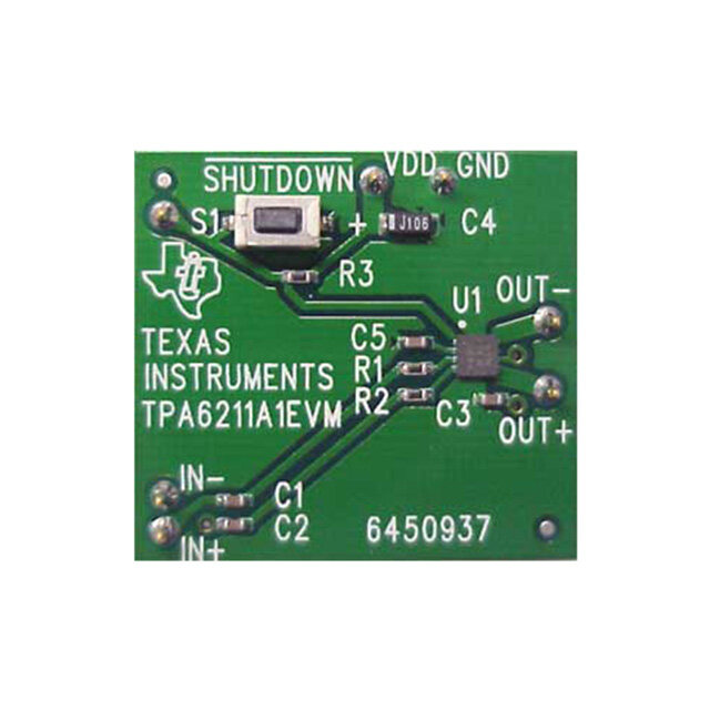
LM48822, LM48822TLEVAL www.ti.com SNAS456C–MAY2008–REVISEDMAY2013 CIN IN_+ VOLUME OUT_ CONTROL AND IN_- MIXER CIN Figure26. Single-EndedInputConfiguration PCB LAYOUT CONFIGURATION Minimize trace impedance of the power, ground and all output traces for optimum performance. Voltage loss due to trace resistance between the LM48822 and the load results in decreased output power and efficiency. Trace resistance between the power supply and ground has the same effect as a poorly regulated supply, increased rippleandreducedpeakoutputpower.Usewidetracesforpowersupplyinputsandamplifieroutputstominimize losses due to trace resistance, as well as route heat away from the device. Proper grounding improves audio performance, minimizes crosstalk between channels and prevents switching noise from interfering with the audio signal.Useofpowerandgroundplanesisrecommended. Place all digital components and route digital signal traces as far as possible from analog components and traces. Do not run digital and analog traces in parallel on the same PCB layer. If digital and analog signal lines mustcrosseitheroverorundereachother,ensurethattheycrossinaperpendicularfashion. LM48822TL Demoboard of Materials Table5.LM48822TLDemoboardBillofMaterials Designator Quantity Description 10µF±10%16V500ΩTantalumCapacitor(BCase)AVX C1 1 TPSB106K016R0500 1μF±10%16VX5RCeramicCapacitor(603)Panasonic C2 1 ECJ-1VB1C105K 2.2μF±10%10VX5RCeramicCapacitor(603)Panasonic C3,C8,C9 3 ECJ-1VB1A225K 1μF±10%16VX7RCeramicCapacitor(1206)Panasonic C4—C7 4 ECJ-3YB1C105K 5kΩ±5%1/10WThickFilmResistor(603)Vishay R1,R2 2 CRCW06035R1KJNEA J1 1 StereoHeadphoneJack J2 1 16-PinBoardmountSocket3M8516-4500JL JU1 1 3PinHeader JU2 1 2PinHeader LM4822TL 1 LM48822TL(16-BumpDSBGA) Copyright©2008–2013,TexasInstrumentsIncorporated SubmitDocumentationFeedback 15 ProductFolderLinks:LM48822 LM48822TLEVAL
LM48822, LM48822TLEVAL SNAS456C–MAY2008–REVISEDMAY2013 www.ti.com Demoboard Schematic U1 VDD OUTL A4 VDD OUTR VDD C1 C2 J1 10 PF 1 PF C2 GND OUTL B1 2L GND C2.32 PF 5A1 C1 BIAS OUTR D1 3CRT C4 4R B3 INL+ COM D4 INL+ 1 PF 1GND JU1 1 C5 B4 INL- C1P A2 2 HEADPHONE_JACK INL- 1 PF 3 C9 C6 2.2 PF HPGND C3 INR+ C1N A1 INR+ 1 PF C7 COM C4 INR- CPVSS B2 INR- 1 PF C8 2.2 PF SCL D2 SCL CPGND A3 VDD GND SDA D3 SDA R1 R2 5k 5k J2 JU2 SDA 1 2 SCL 3 4 5 6 LM48822TL 7 8 9 10 11 12 13 14 15 16 MOUNTING SUPPORT Figure27. LM48822DemoboardSchematic Demonstration Board PCB Layout Figure28.SolderMask Figure29.TopSilkscreen 16 SubmitDocumentationFeedback Copyright©2008–2013,TexasInstrumentsIncorporated ProductFolderLinks:LM48822 LM48822TLEVAL
LM48822, LM48822TLEVAL www.ti.com SNAS456C–MAY2008–REVISEDMAY2013 Figure30.TopLayer Figure31.Layer2(GND) Figure32.Layer3(V ) Figure33.BottomLayer DD Figure34.BottomSilkscreen Revision History Rev Date Description 0.1 04/15/08 InitialPDF. 0.2 04/23/08 Addedthedemoboardsandschematic. 0.3 04/30/08 Textedits. 0.4 07/10/08 Textedits. 0.5 03/09/11 ChangedthebitB7intoB6undertheSHUTDOWNFUNCTIONsection. C 05/02/2013 ChangedlayoutofNationalDataSheettoTIformat. Copyright©2008–2013,TexasInstrumentsIncorporated SubmitDocumentationFeedback 17 ProductFolderLinks:LM48822 LM48822TLEVAL
PACKAGE OPTION ADDENDUM www.ti.com 2-May-2013 PACKAGING INFORMATION Orderable Device Status Package Type Package Pins Package Eco Plan Lead/Ball Finish MSL Peak Temp Op Temp (°C) Top-Side Markings Samples (1) Drawing Qty (2) (3) (4) LM48822TL/NOPB ACTIVE DSBGA YZR 16 250 Green (RoHS SNAGCU Level-1-260C-UNLIM -40 to 85 GK1 & no Sb/Br) LM48822TLX/NOPB ACTIVE DSBGA YZR 16 3000 Green (RoHS SNAGCU Level-1-260C-UNLIM -40 to 85 GK1 & no Sb/Br) (1) The marketing status values are defined as follows: ACTIVE: Product device recommended for new designs. LIFEBUY: TI has announced that the device will be discontinued, and a lifetime-buy period is in effect. NRND: Not recommended for new designs. Device is in production to support existing customers, but TI does not recommend using this part in a new design. PREVIEW: Device has been announced but is not in production. Samples may or may not be available. OBSOLETE: TI has discontinued the production of the device. (2) Eco Plan - The planned eco-friendly classification: Pb-Free (RoHS), Pb-Free (RoHS Exempt), or Green (RoHS & no Sb/Br) - please check http://www.ti.com/productcontent for the latest availability information and additional product content details. TBD: The Pb-Free/Green conversion plan has not been defined. Pb-Free (RoHS): TI's terms "Lead-Free" or "Pb-Free" mean semiconductor products that are compatible with the current RoHS requirements for all 6 substances, including the requirement that lead not exceed 0.1% by weight in homogeneous materials. Where designed to be soldered at high temperatures, TI Pb-Free products are suitable for use in specified lead-free processes. Pb-Free (RoHS Exempt): This component has a RoHS exemption for either 1) lead-based flip-chip solder bumps used between the die and package, or 2) lead-based die adhesive used between the die and leadframe. The component is otherwise considered Pb-Free (RoHS compatible) as defined above. Green (RoHS & no Sb/Br): TI defines "Green" to mean Pb-Free (RoHS compatible), and free of Bromine (Br) and Antimony (Sb) based flame retardants (Br or Sb do not exceed 0.1% by weight in homogeneous material) (3) MSL, Peak Temp. -- The Moisture Sensitivity Level rating according to the JEDEC industry standard classifications, and peak solder temperature. (4) Multiple Top-Side Markings will be inside parentheses. Only one Top-Side Marking contained in parentheses and separated by a "~" will appear on a device. If a line is indented then it is a continuation of the previous line and the two combined represent the entire Top-Side Marking for that device. Important Information and Disclaimer:The information provided on this page represents TI's knowledge and belief as of the date that it is provided. TI bases its knowledge and belief on information provided by third parties, and makes no representation or warranty as to the accuracy of such information. Efforts are underway to better integrate information from third parties. TI has taken and continues to take reasonable steps to provide representative and accurate information but may not have conducted destructive testing or chemical analysis on incoming materials and chemicals. TI and TI suppliers consider certain information to be proprietary, and thus CAS numbers and other limited information may not be available for release. In no event shall TI's liability arising out of such information exceed the total purchase price of the TI part(s) at issue in this document sold by TI to Customer on an annual basis. Addendum-Page 1
PACKAGE MATERIALS INFORMATION www.ti.com 8-May-2013 TAPE AND REEL INFORMATION *Alldimensionsarenominal Device Package Package Pins SPQ Reel Reel A0 B0 K0 P1 W Pin1 Type Drawing Diameter Width (mm) (mm) (mm) (mm) (mm) Quadrant (mm) W1(mm) LM48822TL/NOPB DSBGA YZR 16 250 178.0 8.4 2.08 2.08 0.76 4.0 8.0 Q1 LM48822TLX/NOPB DSBGA YZR 16 3000 178.0 8.4 2.08 2.08 0.76 4.0 8.0 Q1 PackMaterials-Page1
PACKAGE MATERIALS INFORMATION www.ti.com 8-May-2013 *Alldimensionsarenominal Device PackageType PackageDrawing Pins SPQ Length(mm) Width(mm) Height(mm) LM48822TL/NOPB DSBGA YZR 16 250 210.0 185.0 35.0 LM48822TLX/NOPB DSBGA YZR 16 3000 210.0 185.0 35.0 PackMaterials-Page2
MECHANICAL DATA YZR0016xxx D 0.600±0.075 E TLA16XXX (Rev C) D: Max = 1.99 mm, Min = 1.93 mm E: Max = 1.99 mm, Min = 1.93 mm 4215051/A 12/12 NOTES: A.Alllineardimensionsareinmillimeters.DimensioningandtolerancingperASMEY14.5M-1994. B.Thisdrawingissubjecttochangewithoutnotice. www.ti.com
IMPORTANTNOTICE TexasInstrumentsIncorporated(TI)reservestherighttomakecorrections,enhancements,improvementsandotherchangestoits semiconductorproductsandservicesperJESD46,latestissue,andtodiscontinueanyproductorserviceperJESD48,latestissue.Buyers shouldobtainthelatestrelevantinformationbeforeplacingordersandshouldverifythatsuchinformationiscurrentandcomplete. TI’spublishedtermsofsaleforsemiconductorproducts(http://www.ti.com/sc/docs/stdterms.htm)applytothesaleofpackagedintegrated circuitproductsthatTIhasqualifiedandreleasedtomarket.AdditionaltermsmayapplytotheuseorsaleofothertypesofTIproductsand services. ReproductionofsignificantportionsofTIinformationinTIdatasheetsispermissibleonlyifreproductioniswithoutalterationandis accompaniedbyallassociatedwarranties,conditions,limitations,andnotices.TIisnotresponsibleorliableforsuchreproduced documentation.Informationofthirdpartiesmaybesubjecttoadditionalrestrictions.ResaleofTIproductsorserviceswithstatements differentfromorbeyondtheparametersstatedbyTIforthatproductorservicevoidsallexpressandanyimpliedwarrantiesforthe associatedTIproductorserviceandisanunfairanddeceptivebusinesspractice.TIisnotresponsibleorliableforanysuchstatements. BuyersandotherswhoaredevelopingsystemsthatincorporateTIproducts(collectively,“Designers”)understandandagreethatDesigners remainresponsibleforusingtheirindependentanalysis,evaluationandjudgmentindesigningtheirapplicationsandthatDesignershave fullandexclusiveresponsibilitytoassurethesafetyofDesigners'applicationsandcomplianceoftheirapplications(andofallTIproducts usedinorforDesigners’applications)withallapplicableregulations,lawsandotherapplicablerequirements.Designerrepresentsthat,with respecttotheirapplications,Designerhasallthenecessaryexpertisetocreateandimplementsafeguardsthat(1)anticipatedangerous consequencesoffailures,(2)monitorfailuresandtheirconsequences,and(3)lessenthelikelihoodoffailuresthatmightcauseharmand takeappropriateactions.DesigneragreesthatpriortousingordistributinganyapplicationsthatincludeTIproducts,Designerwill thoroughlytestsuchapplicationsandthefunctionalityofsuchTIproductsasusedinsuchapplications. TI’sprovisionoftechnical,applicationorotherdesignadvice,qualitycharacterization,reliabilitydataorotherservicesorinformation, including,butnotlimitedto,referencedesignsandmaterialsrelatingtoevaluationmodules,(collectively,“TIResources”)areintendedto assistdesignerswhoaredevelopingapplicationsthatincorporateTIproducts;bydownloading,accessingorusingTIResourcesinany way,Designer(individuallyor,ifDesignerisactingonbehalfofacompany,Designer’scompany)agreestouseanyparticularTIResource solelyforthispurposeandsubjecttothetermsofthisNotice. TI’sprovisionofTIResourcesdoesnotexpandorotherwisealterTI’sapplicablepublishedwarrantiesorwarrantydisclaimersforTI products,andnoadditionalobligationsorliabilitiesarisefromTIprovidingsuchTIResources.TIreservestherighttomakecorrections, enhancements,improvementsandotherchangestoitsTIResources.TIhasnotconductedanytestingotherthanthatspecifically describedinthepublisheddocumentationforaparticularTIResource. Designerisauthorizedtouse,copyandmodifyanyindividualTIResourceonlyinconnectionwiththedevelopmentofapplicationsthat includetheTIproduct(s)identifiedinsuchTIResource.NOOTHERLICENSE,EXPRESSORIMPLIED,BYESTOPPELOROTHERWISE TOANYOTHERTIINTELLECTUALPROPERTYRIGHT,ANDNOLICENSETOANYTECHNOLOGYORINTELLECTUALPROPERTY RIGHTOFTIORANYTHIRDPARTYISGRANTEDHEREIN,includingbutnotlimitedtoanypatentright,copyright,maskworkright,or otherintellectualpropertyrightrelatingtoanycombination,machine,orprocessinwhichTIproductsorservicesareused.Information regardingorreferencingthird-partyproductsorservicesdoesnotconstitutealicensetousesuchproductsorservices,orawarrantyor endorsementthereof.UseofTIResourcesmayrequirealicensefromathirdpartyunderthepatentsorotherintellectualpropertyofthe thirdparty,oralicensefromTIunderthepatentsorotherintellectualpropertyofTI. TIRESOURCESAREPROVIDED“ASIS”ANDWITHALLFAULTS.TIDISCLAIMSALLOTHERWARRANTIESOR REPRESENTATIONS,EXPRESSORIMPLIED,REGARDINGRESOURCESORUSETHEREOF,INCLUDINGBUTNOTLIMITEDTO ACCURACYORCOMPLETENESS,TITLE,ANYEPIDEMICFAILUREWARRANTYANDANYIMPLIEDWARRANTIESOF MERCHANTABILITY,FITNESSFORAPARTICULARPURPOSE,ANDNON-INFRINGEMENTOFANYTHIRDPARTYINTELLECTUAL PROPERTYRIGHTS.TISHALLNOTBELIABLEFORANDSHALLNOTDEFENDORINDEMNIFYDESIGNERAGAINSTANYCLAIM, INCLUDINGBUTNOTLIMITEDTOANYINFRINGEMENTCLAIMTHATRELATESTOORISBASEDONANYCOMBINATIONOF PRODUCTSEVENIFDESCRIBEDINTIRESOURCESOROTHERWISE.INNOEVENTSHALLTIBELIABLEFORANYACTUAL, DIRECT,SPECIAL,COLLATERAL,INDIRECT,PUNITIVE,INCIDENTAL,CONSEQUENTIALOREXEMPLARYDAMAGESIN CONNECTIONWITHORARISINGOUTOFTIRESOURCESORUSETHEREOF,ANDREGARDLESSOFWHETHERTIHASBEEN ADVISEDOFTHEPOSSIBILITYOFSUCHDAMAGES. UnlessTIhasexplicitlydesignatedanindividualproductasmeetingtherequirementsofaparticularindustrystandard(e.g.,ISO/TS16949 andISO26262),TIisnotresponsibleforanyfailuretomeetsuchindustrystandardrequirements. WhereTIspecificallypromotesproductsasfacilitatingfunctionalsafetyorascompliantwithindustryfunctionalsafetystandards,such productsareintendedtohelpenablecustomerstodesignandcreatetheirownapplicationsthatmeetapplicablefunctionalsafetystandards andrequirements.Usingproductsinanapplicationdoesnotbyitselfestablishanysafetyfeaturesintheapplication.Designersmust ensurecompliancewithsafety-relatedrequirementsandstandardsapplicabletotheirapplications.DesignermaynotuseanyTIproductsin life-criticalmedicalequipmentunlessauthorizedofficersofthepartieshaveexecutedaspecialcontractspecificallygoverningsuchuse. Life-criticalmedicalequipmentismedicalequipmentwherefailureofsuchequipmentwouldcauseseriousbodilyinjuryordeath(e.g.,life support,pacemakers,defibrillators,heartpumps,neurostimulators,andimplantables).Suchequipmentincludes,withoutlimitation,all medicaldevicesidentifiedbytheU.S.FoodandDrugAdministrationasClassIIIdevicesandequivalentclassificationsoutsidetheU.S. TImayexpresslydesignatecertainproductsascompletingaparticularqualification(e.g.,Q100,MilitaryGrade,orEnhancedProduct). Designersagreethatithasthenecessaryexpertisetoselecttheproductwiththeappropriatequalificationdesignationfortheirapplications andthatproperproductselectionisatDesigners’ownrisk.Designersaresolelyresponsibleforcompliancewithalllegalandregulatory requirementsinconnectionwithsuchselection. DesignerwillfullyindemnifyTIanditsrepresentativesagainstanydamages,costs,losses,and/orliabilitiesarisingoutofDesigner’snon- compliancewiththetermsandprovisionsofthisNotice. MailingAddress:TexasInstruments,PostOfficeBox655303,Dallas,Texas75265 Copyright©2017,TexasInstrumentsIncorporated