ICGOO在线商城 > 集成电路(IC) > 线性 - 音頻放大器 > LM4819MX/NOPB

 Datasheet下载
- 型号: LM4819MX/NOPB
- 制造商: Texas Instruments
- 库位|库存: xxxx|xxxx
- 要求:
| 数量阶梯 | 香港交货 | 国内含税 |
| +xxxx | $xxxx | ¥xxxx |
查看当月历史价格
查看今年历史价格
LM4819MX/NOPB产品简介:
ICGOO电子元器件商城为您提供LM4819MX/NOPB由Texas Instruments设计生产,在icgoo商城现货销售,并且可以通过原厂、代理商等渠道进行代购。 LM4819MX/NOPB价格参考¥2.82-¥6.96。Texas InstrumentsLM4819MX/NOPB封装/规格:线性 - 音頻放大器, Amplifier IC 1-Channel (Mono) Class AB 8-SOIC。您可以下载LM4819MX/NOPB参考资料、Datasheet数据手册功能说明书,资料中有LM4819MX/NOPB 详细功能的应用电路图电压和使用方法及教程。
LM4819MX/NOPB 是由 Texas Instruments(德州仪器)生产的一款线性音频放大器,广泛应用于便携式音频设备中。以下是其主要应用场景:

 1. 便携式音频设备
   - MP3 播放器:为耳机或小型扬声器提供高质量的音频输出。
   - 手机和智能手机:作为内置音频放大器驱动扬声器或耳机。
   - 便携式媒体播放器:支持清晰的音频播放,提升用户体验。

 2. 低功耗消费电子
   - 蓝牙音箱:在小型蓝牙音箱中用作功率放大器,提供足够的音量和音质。
   - 语音助手设备:为智能音箱或语音控制设备提供音频输出支持。

 3. 玩具和教育设备
   - 电子学习玩具:用于儿童教育玩具中的声音播放功能。
   - 发声玩具:驱动小型扬声器以产生清晰的声音效果。

 4. 医疗设备
   - 便携式健康监测设备:如血压计、血糖仪等可能需要简单的音频提示功能。
   - 助听器相关设备:提供低失真、高效率的音频信号放大。

 5. 工业应用
   - 人机界面 (HMI):在工业控制器或面板上提供音频反馈。
   - 报警系统:用于小型报警设备的声音输出。

 特点与优势
- 低功耗设计:适合电池供电的便携式设备。
- 高效率:减少热量产生,延长设备续航时间。
- 集成保护功能:如过热保护、短路保护,提高系统可靠性。
- 小尺寸封装:便于集成到空间受限的设计中。

LM4819MX/NOPB 的这些特性使其成为许多需要高效、低功耗音频放大的应用的理想选择。
| 参数 | 数值 |
| 产品目录 | 集成电路 (IC)半导体 |
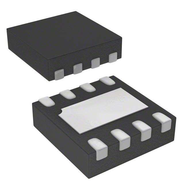
| 描述 | IC AMP AUDIO PWR .35W MONO 8SOIC音频放大器 350mW Audio Pwr Amp |
| 产品分类 | |
| 品牌 | Texas Instruments |
| 产品手册 | http://www.ti.com/lit/gpn/lm4819 |
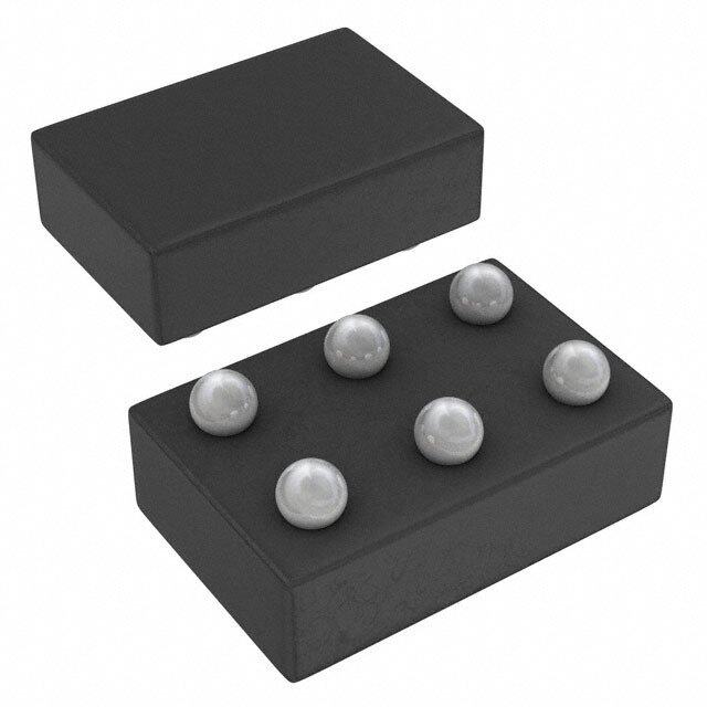
| 产品图片 |
|
| rohs | 符合RoHS无铅 / 符合限制有害物质指令(RoHS)规范要求 |
| 产品系列 | 音频 IC,音频放大器,Texas Instruments LM4819MX/NOPBBoomer® |
| 数据手册 | |
| 产品型号 | LM4819MX/NOPB |
| PCN设计/规格 | |
| THD+噪声 | 1 % |
| 不同负载时的最大输出功率x通道数 | 350mW x 1 @ 16 欧姆 |
| 产品 | Audio Amplifiers |
| 产品种类 | 音频放大器 |
| 供应商器件封装 | 8-SOIC |
| 其它名称 | *LM4819MX/NOPB |
| 包装 | 剪切带 (CT) |
| 商标 | Texas Instruments |
| 安装类型 | 表面贴装 |
| 安装风格 | SMD/SMT |
| 封装 | Reel |
| 封装/外壳 | 8-SOIC(0.154",3.90mm 宽) |
| 封装/箱体 | SOIC-8 Narrow |
| 工作温度 | -40°C ~ 85°C (TA) |
| 工作电源电压 | 3 V, 5 V |
| 工厂包装数量 | 2500 |
| 最大工作温度 | + 85 C |
| 最小工作温度 | - 40 C |
| 标准包装 | 1 |
| 特性 | 消除爆音,差分输入,关闭 |
| 电压-电源 | 2 V ~ 5.5 V |
| 电源电压-最大 | 5.5 V |
| 电源电压-最小 | 2 V |
| 电源电流 | 1.5 mA |
| 电源类型 | Single |
| 类 | Class-AB |
| 类型 | Mono |
| 系列 | LM4819 |
| 输入信号类型 | Single |
| 输出信号类型 | Differential |
| 输出功率 | 350 mW |
| 输出类型 | 1-Channel Mono |
| 通道数量 | 1 Channel |
| 音频负载电阻 | 16 Ohms |


- 商务部:美国ITC正式对集成电路等产品启动337调查
- 曝三星4nm工艺存在良率问题 高通将骁龙8 Gen1或转产台积电
- 太阳诱电将投资9.5亿元在常州建新厂生产MLCC 预计2023年完工
- 英特尔发布欧洲新工厂建设计划 深化IDM 2.0 战略
- 台积电先进制程称霸业界 有大客户加持明年业绩稳了
- 达到5530亿美元!SIA预计今年全球半导体销售额将创下新高
- 英特尔拟将自动驾驶子公司Mobileye上市 估值或超500亿美元
- 三星加码芯片和SET,合并消费电子和移动部门,撤换高东真等 CEO
- 三星电子宣布重大人事变动 还合并消费电子和移动部门
- 海关总署:前11个月进口集成电路产品价值2.52万亿元 增长14.8%


PDF Datasheet 数据手册内容提取
LM4819, LM4819MBD www.ti.com SNAS133D–FEBRUARY2001–REVISEDMARCH2013 LM4819 350mW Audio Power Amplifier with Shutdown Mode CheckforSamples:LM4819,LM4819MBD FEATURES DESCRIPTION 1 • WSON,SOIC,andVSSOPSurfaceMount The LM4819 is a mono bridged power amplifier that 2 is capable of delivering 350mW output power into Packaging RMS a 16Ω load or 300mW output power into an 8Ω • SwitchOn/OffClickSuppression RMS loadwith10%THD+Nfroma5Vpowersupply. • Unity-GainStable The LM4819 Boomer audio power amplifier is • MinimumExternalComponents designed specifically to provide high quality output power and minimize PCB area with surface mount KEY SPECIFICATIONS packaging and a minimal amount of external components. Since the LM4819 does not require • THD+Nat1kHz,350mWContinuousAverage output coupling capacitors, bootstrap capacitors or OutputPowerinto16Ω:10%(max) snubber networks, it is optimally suited for low-power • THD+Nat1kHz,300mWContinuousAverage portableapplications. OutputPowerinto8Ω:10%(max) The closed loop response of the unity-gain stable • ShutdownCurrent:0.7μA(typ) LM4819 can be configured using external gain-setting resistors. The device is available in WSON, VSSOP, APPLICATIONS andSOICpackagetypestosuitvariousapplications. • GeneralPurposeAudio • PortableElectronicDevices • InformationAppliances(IA) Typical Application Figure1. TypicalAudioAmplifierApplicationCircuit Connection Diagrams 1 Pleasebeawarethatanimportantnoticeconcerningavailability,standardwarranty,anduseincriticalapplicationsof TexasInstrumentssemiconductorproductsanddisclaimerstheretoappearsattheendofthisdatasheet. Alltrademarksarethepropertyoftheirrespectiveowners. 2 PRODUCTIONDATAinformationiscurrentasofpublicationdate. Copyright©2001–2013,TexasInstrumentsIncorporated Products conform to specifications per the terms of the Texas Instruments standard warranty. Production processing does not necessarilyincludetestingofallparameters.
LM4819, LM4819MBD SNAS133D–FEBRUARY2001–REVISEDMARCH2013 www.ti.com TopView TopView Figure2.SmallOutline(SOIC)Package Figure3.MiniSmallOutline(VSSOP)Package SeePackageNumberD0008A SeePackageNumberDGK0008A TopView Figure4. WSONPackage SeePackageNumberNGL0008B Thesedeviceshavelimitedbuilt-inESDprotection.Theleadsshouldbeshortedtogetherorthedeviceplacedinconductivefoam duringstorageorhandlingtopreventelectrostaticdamagetotheMOSgates. 2 SubmitDocumentationFeedback Copyright©2001–2013,TexasInstrumentsIncorporated ProductFolderLinks:LM4819 LM4819MBD
LM4819, LM4819MBD www.ti.com SNAS133D–FEBRUARY2001–REVISEDMARCH2013 Absolute Maximum Ratings(1)(2)(3) SupplyVoltage 6.0V StorageTemperature −65°Cto+150°C InputVoltage −0.3VtoV +0.3V DD PowerDissipation(P )(4) InternallyLimited D ESDSusceptibility(5) 3.5kV ESDSusceptibility(6) 250V JunctionTemperature(T) 150°C J SolderingInformation SmallOutlinePackage VaporPhase(60seconds) 215°C Infrared(15seconds) 220°C ThermalResistance θ (VSSOP) 56°C/W JC θ (VSSOP) 210°C/W JA θ (SOIC) 35°C/W JC θ (SOIC) 170°C/W JA θ (WSON) 117°C/W(7) JA θ (WSON) 150°C/W(8) JA (1) Allvoltagesaremeasuredwithrespecttothegroundpin,unlessotherwisespecified. (2) AbsoluteMaximumRatingsindicatelimitsbeyondwhichdamagetothedevicemayoccur.OperatingRatingsindicateconditionsfor whichthedeviceisfunctional,butdonotensurespecificperformancelimits.ElectricalCharacteristicsstateDCandACelectrical specificationsunderparticulartestconditionswhichensurespecificperformancelimits.Thisassumesthatthedeviceiswithinthe OperatingRatings.Specificationsarenotensuredforparameterswherenolimitisgiven.However,thetypicalvalueisagoodindication ofdevice'sperformance. (3) IfMilitary/Aerospacespecifieddevicesarerequired,pleasecontacttheTISalesOffice/Distributorsforavailabilityandspecifications. (4) ThemaximumpowerdissipationmustbederatedatelevatedtemperaturesandisdictatedbyT ,θ ,andtheambienttemperature JMAX JA T .ThemaximumallowablepowerdissipationisP =(T –T )/θ .FortheLM4819,T =150°Candthetypicaljunction-to- A DMAX JMAX A JA JMAX ambientthermalresistance(θ )whenboardmountedis210°C/WfortheVSSOPpackageand170°C/WfortheSOICpackage. JA (5) Humanbodymodel,100pFdischargedthrougha1.5kΩresistor. (6) MachineModel,220pF–240pFcapacitorisdischargedthroughallpins. (7) Thegivenθ isforanLM4819packageinanNGL0008BwiththeExposed-DAPsolderedtoaprintedcircuitboardcopperpadwithan JA areaequivalenttothatoftheExposed-DAPitself.TheExposed-DAPoftheNGL0008Bpackageshouldbeelectricallyconnectedto GNDoranelectricallyisolatedcopperarea. (8) Thegivenθ isforanLM4819packageinanNGL0008BwiththeExposed-DAPnotsolderedtoanyprintedcircuitboardcopper. JA Operating Ratings(1)(2) TemperatureRange −40°C≤T ≤85°C T ≤T ≤T A MIN A MAX SupplyVoltage 2.0V≤V ≤5.5V CC (1) Allvoltagesaremeasuredwithrespecttothegroundpin,unlessotherwisespecified. (2) AbsoluteMaximumRatingsindicatelimitsbeyondwhichdamagetothedevicemayoccur.OperatingRatingsindicateconditionsfor whichthedeviceisfunctional,butdonotensurespecificperformancelimits.ElectricalCharacteristicsstateDCandACelectrical specificationsunderparticulartestconditionswhichensurespecificperformancelimits.Thisassumesthatthedeviceiswithinthe OperatingRatings.Specificationsarenotensuredforparameterswherenolimitisgiven.However,thetypicalvalueisagoodindication ofdevice'sperformance. Copyright©2001–2013,TexasInstrumentsIncorporated SubmitDocumentationFeedback 3 ProductFolderLinks:LM4819 LM4819MBD
LM4819, LM4819MBD SNAS133D–FEBRUARY2001–REVISEDMARCH2013 www.ti.com Electrical Characteristics V = 5V(1)(2) DD ThefollowingspecificationsapplyforV =5V,R =16Ωunlessotherwisestated.LimitsapplyforT =25°C. DD L A LM4819 Units Parameter TestConditions Typical(3) Limit(4)(5) (Limits) I QuiescentPowerSupplyCurrent V =0V,I =0A 1.5 3.0 mA(max) DD IN o I ShutdownCurrent V =V (6) 1.0 5.0 µA(max) SD PIN1 DD V ShutdownVoltageInputHigh 4.0 V(min) SDIH V ShutdownVoltageInputLow 1.0 V(max) SDIL V OutputOffsetVoltage V =0V 5 50 mV(max) OS IN THD=10%,f =1kHz 350 mW IN P OutputPower O THD=10%,f =1kHz,R =8Ω 300 mW IN L THD+N TotalHarmonicDistortion+Noise P =270mW ,A =2,f =1kHz 1 % O RMS VD IN (1) Allvoltagesaremeasuredwithrespecttothegroundpin,unlessotherwisespecified. (2) AbsoluteMaximumRatingsindicatelimitsbeyondwhichdamagetothedevicemayoccur.OperatingRatingsindicateconditionsfor whichthedeviceisfunctional,butdonotensurespecificperformancelimits.ElectricalCharacteristicsstateDCandACelectrical specificationsunderparticulartestconditionswhichensurespecificperformancelimits.Thisassumesthatthedeviceiswithinthe OperatingRatings.Specificationsarenotensuredforparameterswherenolimitisgiven.However,thetypicalvalueisagoodindication ofdevice'sperformance. (3) Typicalspecificationsarespecifiedat25°Candrepresenttheparametricnorm. (4) TestedlimitsarespecifiedtoTI'sAOQL(AverageOutgoingQualityLevel). (5) Datasheetmin/maxspecificationlimitsarespecifiedbydesigns,test,orstatisticalanalysis. (6) Theshutdownpin(pin1)shouldbedrivenascloseaspossibletoV forminimumcurrentinShutdownMode. DD Electrical Characteristics V = 3V(1)(2) DD ThefollowingspecificationsapplyforV =3VandR =16Ωloadunlessotherwisestated.LimitsapplytoT =25°C. DD L A LM4819 Units Parameter TestConditions Typical(3) Limit(4)(5) (Limits) I QuiescentPowerSupplyCurrent V =0V,I =0A 1.0 3.0 mA(max) DD IN o I ShutdownCurrent V =V (6) 0.7 5.0 µA(max) SD PIN1 DD V ShutdownVoltageInputHigh 2.4 V(min) SDIH V ShutdownVoltageInputLow 0.6 V(max) SDIL V OutputOffsetVoltage V =0V 5 50 mV OS IN THD=10%,f =1kHz 110 mW IN P OutputPower O THD=10%,f =1kHz,R =8Ω 90 mW IN L THD+N TotalHarmonicDistortion+Noise P =80mW ,A =2,f =1kHz 1 % O RMS VD IN (1) Allvoltagesaremeasuredwithrespecttothegroundpin,unlessotherwisespecified. (2) AbsoluteMaximumRatingsindicatelimitsbeyondwhichdamagetothedevicemayoccur.OperatingRatingsindicateconditionsfor whichthedeviceisfunctional,butdonotensurespecificperformancelimits.ElectricalCharacteristicsstateDCandACelectrical specificationsunderparticulartestconditionswhichensurespecificperformancelimits.Thisassumesthatthedeviceiswithinthe OperatingRatings.Specificationsarenotensuredforparameterswherenolimitisgiven.However,thetypicalvalueisagoodindication ofdevice'sperformance. (3) Typicalspecificationsarespecifiedat25°Candrepresenttheparametricnorm. (4) TestedlimitsarespecifiedtoTI'sAOQL(AverageOutgoingQualityLevel). (5) Datasheetmin/maxspecificationlimitsarespecifiedbydesigns,test,orstatisticalanalysis. (6) Theshutdownpin(pin1)shouldbedrivenascloseaspossibletoV forminimumcurrentinShutdownMode. DD 4 SubmitDocumentationFeedback Copyright©2001–2013,TexasInstrumentsIncorporated ProductFolderLinks:LM4819 LM4819MBD
LM4819, LM4819MBD www.ti.com SNAS133D–FEBRUARY2001–REVISEDMARCH2013 External Components Description (SeeFigure1) Components FunctionalDescription 1. R CombinedwithR,thisinvertinginputresistorsetstheclosed-loopgain.R alsoformsahighpassfilterwithC atf = i f i i c 1/(2πRC). i i 2. C ThisinputcouplingcapacitorblocksDCvoltageattheamplifier'sterminals.CombinedwithR,itcreatesahighpass i i filterwithR atf =1/(2πRC).Refertothesection,ProperSelectionofExternalComponentsforanexplanationofhow i c i i todeterminethevalueofC. i 3. R CombinedwithR,thisisthefeedbackresistorthatsetstheclosed-loopgain:A =2(R /R). f i v F i 4. C Thisisthepowersupplybypasscapacitorthatfiltersthevoltageappliedtothepowersupplypin.Refertothe S ApplicationInformationsectionforproperplacementandselectionofC. s 5. C ThisisthebypasspincapacitorthatfiltersthevoltageattheBYPASSpin.Refertothesection,ProperSelectionof B ExternalComponents,forinformationconcerningproperplacementandselectionofC . B Copyright©2001–2013,TexasInstrumentsIncorporated SubmitDocumentationFeedback 5 ProductFolderLinks:LM4819 LM4819MBD
LM4819, LM4819MBD SNAS133D–FEBRUARY2001–REVISEDMARCH2013 www.ti.com Typical Performance Characteristics THD+NvsFrequency THD+NvsFrequency Figure5. Figure6. THD+NvsFrequency THD+NvsFrequency Figure7. Figure8. THD+NvsFrequency THD+NvsFrequency Figure9. Figure10. 6 SubmitDocumentationFeedback Copyright©2001–2013,TexasInstrumentsIncorporated ProductFolderLinks:LM4819 LM4819MBD
LM4819, LM4819MBD www.ti.com SNAS133D–FEBRUARY2001–REVISEDMARCH2013 Typical Performance Characteristics (continued) THD+NvsOutputPower THD+NvsOutputPower Figure11. Figure12. THD+NvsOutputPower THD+NvsOutputPower Figure13. Figure14. THD+NvsOutputPower THD+NvsOutputPower Figure15. Figure16. Copyright©2001–2013,TexasInstrumentsIncorporated SubmitDocumentationFeedback 7 ProductFolderLinks:LM4819 LM4819MBD
LM4819, LM4819MBD SNAS133D–FEBRUARY2001–REVISEDMARCH2013 www.ti.com Typical Performance Characteristics (continued) OutputPowervsSupplyVoltage OutputPowervsSupplyVoltage R =8Ω R =16Ω L L Figure17. Figure18. OutputPowervsSupplyVoltage R =32Ω OutputPowervsLoadResistance L Figure19. Figure20. PowerDissipationvs PowerDissipationvs OutputPower OutputPower V =5V V =3V DD DD Figure21. Figure22. 8 SubmitDocumentationFeedback Copyright©2001–2013,TexasInstrumentsIncorporated ProductFolderLinks:LM4819 LM4819MBD
LM4819, LM4819MBD www.ti.com SNAS133D–FEBRUARY2001–REVISEDMARCH2013 Typical Performance Characteristics (continued) FrequencyResponsevs PowerDeratingCurves InputCapacitorSize Figure23. Figure24. SupplyCurrentvs SupplyVoltage Figure25. Copyright©2001–2013,TexasInstrumentsIncorporated SubmitDocumentationFeedback 9 ProductFolderLinks:LM4819 LM4819MBD
LM4819, LM4819MBD SNAS133D–FEBRUARY2001–REVISEDMARCH2013 www.ti.com APPLICATION INFORMATION BRIDGE CONFIGURATION EXPLANATION As shown in Figure 1, the LM4819 consists of two operational amplifiers. External resistors, R and R set the i F closed-loop gain of the first amplifier (and the amplifier overall), whereas two internal 20kΩ resistors set the second amplifier's gain at -1. The LM4819 is typically used to drive a speaker connected between the two amplifieroutputs. Figure 1 shows that the output of Amp1 servers as the input to Amp2, which results in both amplifiers producing signals identical in magnitude but 180° out of phase. Taking advantage of this phase difference, a load is placed between V and V and driven differentially (commonly referred to as "bridge mode"). This results in a 01 02 differentialgainof A =2*(R/R) (1) VD f i Bridge mode is different from single-ended amplifiers that drive loads connected between a single amplifier's output and ground. For a given supply voltage, bridge mode has a distinct advantage over the single-ended configuration: its differential output doubles the voltage swing across the load. This results in four times the output power when compared to a single-ended amplifier under the same conditions. This increase in attainable output assumes that the amplifier is not current limited or the output signal is not clipped. To ensure minimum output signal clipping when choosing an amplifier's closed-loop gain, refer to the Audio Power Amplifier Design Examplesection. AnotheradvantageofthedifferentialbridgeoutputisnonetDCvoltageacrosstheload.Thisresultsfrombiasing V and V at half-supply. This eliminates the coupling capacitor that single supply, single-ended amplifiers 01 02 require. Eliminating an output coupling capacitor in a single-ended configuration forces a single supply amplifier's half-supply bias voltage across the load. The current flow created by the half-supply bias voltage increases internalICpowerdissipationandmaypermanentlydamageloadssuchasspeakers. POWER DISSIPATION Power dissipation is a major concern when designing a successful bridged or single-ended amplifier. Equation 2 states the maximum power dissipation point for a single-ended amplifier operating at a given supply voltage and drivingaspecifiedload. P =(V )2/(2π2R )(W)Single-ended (2) DMAX DD L However,adirectconsequenceoftheincreasedpowerdeliveredtotheloadbyabridgedamplifierisanincrease in the internal power dissipation point for a bridge amplifier operating at the same given conditions. Equation 3 states the maximum power dissipation point for a bridged amplifier operating at a given supply voltage and drivingaspecifiedload. P =4(V )2/(2π2R )(W)BridgeMode (3) DMAX DD L The LM4819 has two operational amplifiers in one package and the maximum internal power dissipation is four times that of a single-ended amplifier. However, even with this substantial increase in power dissipation, the Lm4819 does not require heatsinking. From Equation 3, assuming a 5V power supply and an 8Ω load, the maximum power dissipation point is 633mW. The maximum power dissipation point obtained from Equation 3 mustnotexceedthepowerdissipationpredictedbyEquation4: P =(T -T )/θ (W) (4) DMAX JMAX A JA ForthemicroDGK0008Apackage,θ =210°C/W,fortheD0008Apackage,θ =170°C/W,andT =150°C JA JA JMAX for the LM4819. For a given ambient temperature, T , Equation 4 can be used to find the maximum internal A power dissipation supported by the IC packaging. If the result of Equation 3 is greater than the result of Equation 4, then decrease the supply voltage, increase the load impedance, or reduce the ambient temperature. For a typical application using the D0008A packaged LM4819 with a 5V power supply and an 8Ω load, the maximum ambient temperature that does not violate the maximum junction temperature is approximately 42°C. If a DGK0008A packaged part is used instead with the same supply voltage and load, the maximum ambient temperature is 17°C. In both cases, it is assumed that a device is a surface mount part operating around the maximum power dissipation point. The assumption that the device is operating around the maximum power dissipation point is incorrect for an 8Ω load. The maximum power dissipation point occurs when the output power is equal to the maximum power dissipation or 50% efficiency. The LM4819 is not capable of the output power level (633mW) required to operate at the maximum power dissipation point for an 8Ω load. To find the maximum power dissipation, the graph Figure 22 must be used. From the graph, the maximum power dissipation for an 8Ω 10 SubmitDocumentationFeedback Copyright©2001–2013,TexasInstrumentsIncorporated ProductFolderLinks:LM4819 LM4819MBD
LM4819, LM4819MBD www.ti.com SNAS133D–FEBRUARY2001–REVISEDMARCH2013 load and a 5V supply is approximately 575mW. Substituting this value back into Equation 4 for P and using DMAX θ = 210°C/W for the DGK0008A package, the maximum ambient temperature is calculated to be 29°C. Using JA θ = 170°C/W for the D0008A package, the maximum ambient temperature is 52°C. Refer to the Typical JA Performance Characteristics curves for power dissipation information for lower output powers and maximum powerdissipationforeachpackageatagivenambienttemperature. POWER SUPPLY BYPASSING As with any power amplifier, proper supply bypassing is critical for low noise performance and high power supply rejection. The capacitors connected to the bypass and power supply pins should be placed as close to the LM4819 as possible. The capacitor connected between the bypass pin and ground improves the internal bias voltage's stability, producing improved PSRR. The improvements to PSRR increase as the bypass pin capacitor value increases. Typical applications employ a 5V regulator with 10µF and 0.1µF filter capacitors that aid in supply stability. Their presence, however, does not eliminate the need for bypassing the supply nodes of the LM4819. The selection of bypass capacitor values, especially C , depends on desired PSRR requirements, click B and pop performance as explained in the section, Proper Selection of External Components, as well as system costandsizeconstraints. SHUTDOWN FUNCTION The voltage applied to the LM4819's SHUTDOWN pin controls the shutdown function. Activate micro-power shutdown by applying V to the SHUTDOWN pin. When active, the LM4819's micro-power shutdown feature DD turns off the amplifier's bias circuitry, reducing the supply current. The logic threshold is typically 1/2V . The low DD 0.7µA typical shutdown current is achieved by applying a voltage that is as near as V as possible to the DD SHUTDOWN pin. A voltage that is less than V may increase the shutdown current. Avoid intermittent or DD unexpected micro-power shutdown by ensuring that the SHUTDOWN pin is not left floating but connected to eitherV orGND. DD Thereareafewwaystoactivatemicro-powershutdown.Theseincludedusingasingle-pole,single-throwswitch, a microcontroller, or a microprocessor. When using a switch, connect an external 10kΩ to 100kΩ pull-up resistor between the SHUTDOWN pin and V . Connect the switch between the SHUTDOWN pin and ground. Select DD normal amplifier operation by closing the switch. Opening the switch connects the shutdown pin to V through DD the pull-up resistor, activating micro-power shutdown. The switch and resistor ensure that the SHUTDOWN pin will not float. This prevents unwanted state changes. In a system with a microprocessor or a microcontroller, use a digital output to apply the control voltage to the SHUTDOWN pin. Driving the SHUTDOWN pin with active circuitryeliminatesthepull-upresistor PROPER SELECTION OF EXTERNAL COMPONENTS Optimizing the LM4819's performance requires properly selecting external components. Though the LM4819 operates well when using external components with wide tolerances, best performance is achieved by optimizing componentvalues. The LM4819 is unity gain stable, giving the designer maximum design flexibility. The gain should be set to no more than a given application requires. This allows the amplifier to achieve minimum THD+N and maximum signal-to-noise ratio. These parameters are compromised as the closed-loop gain increases. However, low gain demands input signals with greater voltage swings to achieve maximum output power. Fortunately, many signal sources such as audio CODECs have outputs of 1V (2.83V ). Please refer to the Audio Power Amplifier RMS P-P Designsectionformoreinformationonselectingthepropergain. Another important consideration is the amplifier's close-loop bandwidth. To a large extent, the bandwidth is dictated by the choice of external components shown in Figure 1. The input coupling capacitor, C, forms a first i order high pass filter that limits low frequency response. This value should be chosen based on needed frequencyresponseforafewdistinctreasonsdiscussedbelow InputCapacitorValueSelection Amplifying the lowest audio frequencies requires a high value input coupling capacitor (C in Figure 1). A high i value capacitor can be expensive and may compromise space efficiency in portable designs. In many cases the speakers used in portable systems, whether internal or external, have little ability to reproduce signals below 150Hz. Applications using speakers with limited frequency response reap little improvement by using a large inputcapacitor. Copyright©2001–2013,TexasInstrumentsIncorporated SubmitDocumentationFeedback 11 ProductFolderLinks:LM4819 LM4819MBD
LM4819, LM4819MBD SNAS133D–FEBRUARY2001–REVISEDMARCH2013 www.ti.com Besides affecting system cost and size, C has an effect on the LM4819's click and pop performance. When the i supplyvoltageisfirstapplied,atransient(pop)iscreatedasthechargeontheinputcapacitorchangesfromzero to a quiescent state. The magnitude of the pop is directly proportional to the input capacitor's value. Higher value capacitors need more time to reach a quiescent DC voltage (usually 1/2 V ) when charged with a fixed current. DD The amplifier's output charges the input capacitor through the feedback resistor, R . Thus, selecting an input F capacitorvaluethatisnohigherthannecessarytomeetthedesired-3dBfrequencycanminimizepops. As shown in Figure 1, the input resistor (R) and the input capacitor, C produce a -3dB high pass filter cutoff i i frequencythatisfoundusingEquation5. f =1/(2πRC)(Hz) (5) -3dB i i As an example when using a speaker with a low frequency limit of 150Hz, C, using Equation 5 is 0.063µF. The i 0.39µF C shown in Figure 1 allows the LM4819 to drive a high efficiency, full range speaker whose response i extendsdownto20Hz. Besides optimizing the input capacitor value, the bypass capacitor value, C requires careful consideration. The B bypass capacitor's value is the most critical to minimizing turn-on pops because it determines how fast the LM4819 turns on. The slower the LM4819's outputs ramp to their quiescent DC voltage (nominally 1/2V ), the DD smaller the turn-on pop. While the device will function properly (no oscillations or motorboating), with C less B than 1.0µF, the device will be much more susceptible to turn-on clicks and pops. Thus, a value of C equal to or B greaterthan1.0µFisrecommendedinallbutthemostcostsensitivedesigns. BypassCapacitorValueSelection Besidesminimizingtheinputcapacitorsize,carefulconsiderationshouldbepaidtothevalueofC ,thecapacitor B connected to the BYPASS pin. Since C determines how fast the LM4819 settles to quiescent operation, its B value is critical when minimizing turn-on pops. The slower the LM4819's outputs ramp to their quiescent DC voltage (nominally 1/2V ), the smaller the turn-on pop. Choosing C equal to 1.0µF along with a small value of DD B C (in the range of 0.1µF to 0.39µF) produces a click-less and pop-less shutdown function. As discussed above, i choosingC nolargerthannecessaryforthedesiredbandwidthhelpsminimizeclicksandpops. i OptimizingClickandPopReductionPerformance The LM4819 contains circuitry that minimizes turn-on and shutdown transients or "clicks and pops". For this discussion, turn on refers to either applying the power or supply voltage or when the shutdown mode is deactivated. While the power supply is ramping to it's final value, the LM4819's internal amplifiers are configured as unity gain buffers. An internal current source charges the voltage of the bypass capacitor, C , connected to B the BYPASS pin in a controlled, linear manner. Ideally, the input and outputs track the voltage charging on the bypass capacitor. The gain of the internal amplifiers remains unity until the bypass capacitor is fully charged to 1/2V . As soon as the voltage on the bypass capacitor is stable, the device becomes fully operational. Although DD the BYPASS pin current cannot be modified, changing the size of the bypass capacitor, C , alters the device's B turn-on time and magnitude of "clicks and pops". Increasing the value of C reduces the magnitude of turn-on B pops. However, this presents a tradeoff: as the size of C increases, the turn-on time (Ton) increases. There is a B linear relationship between the size of C and the turn on time. Below are some typical turn-on times for various B valuesofC : B C T B ON 0.01µF 20ms 0.1µF 200ms 0.22µF 440ms 0.47µF 940ms 1.0µF 2S 12 SubmitDocumentationFeedback Copyright©2001–2013,TexasInstrumentsIncorporated ProductFolderLinks:LM4819 LM4819MBD
LM4819, LM4819MBD www.ti.com SNAS133D–FEBRUARY2001–REVISEDMARCH2013 In order to eliminate "clicks and pops", all capacitors must be discharged before turn-on. Rapidly switching V DD maynotallowthecapacitorstofullydischarge,whichmaycause"clicksandpops". AUDIO POWER AMPLIFIER DESIGN EXAMPLE Thefollowingarethedesiredoperationalparameters: Given: PowerOutput 100mW LoadImpedance 16Ω InputLevel 1Vrms(max) InputImpedance 20kΩ Bandwidth 100Hz–20kHz ±0.25dB The design begins by specifying the minimum supply voltage necessary to obtain the specified output power. To find this minimum supply voltage, use the Output Power vs. Supply Voltage graph in the Typical Performance Characteristics section. From the graph for a 16Ω load, (graphs are for 8Ω, 16Ω, and 32Ω loads) the supply voltagefor100mWofoutputpowerwith1%THD+Nisapproximately3.15volts. Additional supply voltage creates the benefit of increased headroom that allows the LM4819 to reproduce peaks in excess of 100mW without output signal clipping or audible distortion. The choice of supply voltage must also notcreateasituationthatviolatesmaximumdissipationasexplainedaboveinthePowerDissipationsection.For example, if a 3.3V supply is chosen for extra headroom then according to Equation 3 the maximum power dissipation point with a 16Ω load is 138mW. Using Equation 4 the maximum ambient temperature is 121°C for theDGK0008Apackageand126°CfortheD0008Apackage. After satisfying the LM4819's power dissipation requirements, the minimum differential gain is found using Equation6. (6) Thus a minimum gain of 1.27 V/V allows the LM4819 to reach full output swing and maintain low noise and THD+N performance. For this example, let A = 1.27. The amplifier's overall gain is set using the input (R) and VD i feedback (R ) resistors. With the desired input impedance set to 20kΩ, the feedback resistor is found using F Equation7. R /R =A /2(V/V) (7) F i VD ThevalueofR is13kΩ. F The last step in this design example is setting the amplifier's -3dB frequency bandwidth. To achieve the desired ±0.25dB pass band magnitude variation limit, the low frequency response must extend to at least one-fifth the lower bandwidth limit and the high frequency response must extend to at least five times the upper bandwidth limit.Thegainvariationforbothresponselimitsis0.17dB,wellwithinthe±0.25dBdesiredlimit. Theresultsare: f =100Hz/5=20Hz L f =20kHz*5=100kHz H As mentioned in the External Components section, R and C create a high pass filter that sets the amplifier's i i lowerbandpassfrequencylimit.Findthecouplingcapacitor'svalueusingEquation8. C ≥1/(2πRf)(F) (8) i ic C ≥ 0.398µF, a standard value of 0.39µF will be used. The product of the desired high frequency cutoff (100kHz i in this example) and the differential gain, A , determines the upper pass band response limit. With A = 1.27 VD VD and f = 100kHz, the closed-loop gain bandwidth product (GBWP) is 127kHz. This is less than the LM4819's H 900kHz GBWP. With this margin the amplifier can be used in designs that require more differential gain while avoidingperformancerestrictingbandwidthlimitations. Copyright©2001–2013,TexasInstrumentsIncorporated SubmitDocumentationFeedback 13 ProductFolderLinks:LM4819 LM4819MBD
LM4819, LM4819MBD SNAS133D–FEBRUARY2001–REVISEDMARCH2013 www.ti.com Figure26. HigherGainAudioAmplifier The LM4819 is unity-gain stable and requires no external components besides gain-setting resistors, an input coupling capacitor, and proper supply bypassing in the typical application. However, if a closed-loop differential gain of greater than 10 is required, a feedback capacitor (C ) may be needed as shown in Figure 26 to 4 bandwidth limit the amplifier. This feedback capacitor creates a low pass filter that eliminates possible high frequency oscillations. Care should be taken when calculating the -3dB frequency in that an incorrect combination of R and C will cause rolloff before 20kHz. A typical combination of feedback resistor and 3 4 capacitor that will not produce audio band high frequency rolloff is R = 20kΩ and C = 25pF. These components 3 4 result in a -3dB point of approximately 320 kHz. It is not recommended that the feedback resistor and capacitor beusedtoimplementabandlimitingfilterbelow100kHz. Figure27. DifferentialAmplifierConfigurationforLM4819 14 SubmitDocumentationFeedback Copyright©2001–2013,TexasInstrumentsIncorporated ProductFolderLinks:LM4819 LM4819MBD
LM4819, LM4819MBD www.ti.com SNAS133D–FEBRUARY2001–REVISEDMARCH2013 Figure28. ReferenceDesignBoardandPCBLayoutGuidelines LM4819 SOIC DEMO BOARD ARTWORK Figure29. SilkScreen Figure30. TopLayer Copyright©2001–2013,TexasInstrumentsIncorporated SubmitDocumentationFeedback 15 ProductFolderLinks:LM4819 LM4819MBD
LM4819, LM4819MBD SNAS133D–FEBRUARY2001–REVISEDMARCH2013 www.ti.com Figure31. BottomLayer LM4819 VSSOP DEMO BOARD ARTWORK Figure32. SilkScreen Figure33. TopLayer 16 SubmitDocumentationFeedback Copyright©2001–2013,TexasInstrumentsIncorporated ProductFolderLinks:LM4819 LM4819MBD
LM4819, LM4819MBD www.ti.com SNAS133D–FEBRUARY2001–REVISEDMARCH2013 Figure34. BottomLayer LM4819 WSON DEMO BOARD ARTWORK CompositeView TopLayer SilkScreen BottomLayer Table1.MonoLM4819ReferenceDesignBoards BillofMaterialforallDemoBoards Item PartNumber PartDescription Qty RefDesignator 1 551011208-001 LM4819MonoReferenceDesignBoard 1 10 482911183-001 LM4819AudioAMP 1 U1 20 151911207-001 TantCap1uF16V10 1 C1 Copyright©2001–2013,TexasInstrumentsIncorporated SubmitDocumentationFeedback 17 ProductFolderLinks:LM4819 LM4819MBD
LM4819, LM4819MBD SNAS133D–FEBRUARY2001–REVISEDMARCH2013 www.ti.com Table1.MonoLM4819ReferenceDesignBoards BillofMaterialforallDemoBoards(continued) Item PartNumber PartDescription Qty RefDesignator 21 151911207-002 CerCap0.39uF50VZ5U20%1210 1 C2 25 152911207-001 TantCap1uF16V10 1 C3 30 472911207-001 Res20KOhm1/10W5 3 R1,R2,R3 35 210007039-002 JumperHeaderVerticalMount2X10.100 2 J1,J2 PCB LAYOUT GUIDELINES This section provides practical guidelines for mixed signal PCB layout that involves various digital/analog power and ground traces. Designers should note that these are only "rule-of-thumb" recommendations and the actual resultswilldependheavilyonthefinallayout. GeneralMixedSignalLayoutRecommendation PowerandGroundCircuits For two layer mixed signal design, it is important to isolate the digital power and ground trace paths from the analog power and ground trace paths. Star trace routing techniques (bringing individual traces back to a central point rather than daisy chaining traces together in a serial manner) can have a major impact on low level signal performance. Star trace routing refers to using individual traces to feed power and ground to each circuit or even device. This technique will take require a greater amount of design time but will not increase the final price of the board.Theonlyextrapartsrequiredwillbesomejumpers. Single-PointPower/GroundConnections The analog power traces should be connected to the digital traces through a single point (link). A "Pi-filter" can be helpful in minimizing high frequency noise coupling between the analog and digital sections. It is further recommended to put digital and analog power traces over the corresponding digital and analog ground traces to minimizenoisecoupling. PlacementofDigitalandAnalogComponents All digital components and high-speed digital signals traces should be located as far away as possible from analogcomponentsandcircuittraces. AvoidingTypicalDesign/LayoutProblems Avoid ground loops or running digital and analog traces parallel to each other (side-by-side) on the same PCB layer. When traces must cross over each other do it at 90 degrees. Running digital and analog traces at 90 degrees to each other from the top to the bottom side as much as possible will minimize capacitive noise couplingandcrosstalk. 18 SubmitDocumentationFeedback Copyright©2001–2013,TexasInstrumentsIncorporated ProductFolderLinks:LM4819 LM4819MBD
LM4819, LM4819MBD www.ti.com SNAS133D–FEBRUARY2001–REVISEDMARCH2013 REVISION HISTORY ChangesfromRevisionC(March2013)toRevisionD Page • ChangedlayoutofNationalDataSheettoTIformat.......................................................................................................... 18 Copyright©2001–2013,TexasInstrumentsIncorporated SubmitDocumentationFeedback 19 ProductFolderLinks:LM4819 LM4819MBD
PACKAGE OPTION ADDENDUM www.ti.com 6-Feb-2020 PACKAGING INFORMATION Orderable Device Status Package Type Package Pins Package Eco Plan Lead/Ball Finish MSL Peak Temp Op Temp (°C) Device Marking Samples (1) Drawing Qty (2) (6) (3) (4/5) LM4819LD/NOPB ACTIVE WSON NGL 8 1000 Green (RoHS SN Level-3-260C-168 HR -40 to 85 G19 & no Sb/Br) LM4819MM/NOPB ACTIVE VSSOP DGK 8 1000 Green (RoHS SN Level-1-260C-UNLIM -40 to 85 G19 & no Sb/Br) LM4819MMX/NOPB ACTIVE VSSOP DGK 8 3500 Green (RoHS SN Level-1-260C-UNLIM -40 to 85 G19 & no Sb/Br) LM4819MX/NOPB ACTIVE SOIC D 8 2500 Green (RoHS SN Level-1-260C-UNLIM -40 to 85 LM48 & no Sb/Br) 19M (1) The marketing status values are defined as follows: ACTIVE: Product device recommended for new designs. LIFEBUY: TI has announced that the device will be discontinued, and a lifetime-buy period is in effect. NRND: Not recommended for new designs. Device is in production to support existing customers, but TI does not recommend using this part in a new design. PREVIEW: Device has been announced but is not in production. Samples may or may not be available. OBSOLETE: TI has discontinued the production of the device. (2) RoHS: TI defines "RoHS" to mean semiconductor products that are compliant with the current EU RoHS requirements for all 10 RoHS substances, including the requirement that RoHS substance do not exceed 0.1% by weight in homogeneous materials. Where designed to be soldered at high temperatures, "RoHS" products are suitable for use in specified lead-free processes. TI may reference these types of products as "Pb-Free". RoHS Exempt: TI defines "RoHS Exempt" to mean products that contain lead but are compliant with EU RoHS pursuant to a specific EU RoHS exemption. Green: TI defines "Green" to mean the content of Chlorine (Cl) and Bromine (Br) based flame retardants meet JS709B low halogen requirements of <=1000ppm threshold. Antimony trioxide based flame retardants must also meet the <=1000ppm threshold requirement. (3) MSL, Peak Temp. - The Moisture Sensitivity Level rating according to the JEDEC industry standard classifications, and peak solder temperature. (4) There may be additional marking, which relates to the logo, the lot trace code information, or the environmental category on the device. (5) Multiple Device Markings will be inside parentheses. Only one Device Marking contained in parentheses and separated by a "~" will appear on a device. If a line is indented then it is a continuation of the previous line and the two combined represent the entire Device Marking for that device. (6) Lead/Ball Finish - Orderable Devices may have multiple material finish options. Finish options are separated by a vertical ruled line. Lead/Ball Finish values may wrap to two lines if the finish value exceeds the maximum column width. Important Information and Disclaimer:The information provided on this page represents TI's knowledge and belief as of the date that it is provided. TI bases its knowledge and belief on information provided by third parties, and makes no representation or warranty as to the accuracy of such information. Efforts are underway to better integrate information from third parties. TI has taken and Addendum-Page 1
PACKAGE OPTION ADDENDUM www.ti.com 6-Feb-2020 continues to take reasonable steps to provide representative and accurate information but may not have conducted destructive testing or chemical analysis on incoming materials and chemicals. TI and TI suppliers consider certain information to be proprietary, and thus CAS numbers and other limited information may not be available for release. In no event shall TI's liability arising out of such information exceed the total purchase price of the TI part(s) at issue in this document sold by TI to Customer on an annual basis. Addendum-Page 2
PACKAGE MATERIALS INFORMATION www.ti.com 4-Aug-2019 TAPE AND REEL INFORMATION *Alldimensionsarenominal Device Package Package Pins SPQ Reel Reel A0 B0 K0 P1 W Pin1 Type Drawing Diameter Width (mm) (mm) (mm) (mm) (mm) Quadrant (mm) W1(mm) LM4819LD/NOPB WSON NGL 8 1000 178.0 12.4 2.8 2.8 1.0 8.0 12.0 Q1 LM4819MM/NOPB VSSOP DGK 8 1000 178.0 12.4 5.3 3.4 1.4 8.0 12.0 Q1 LM4819MMX/NOPB VSSOP DGK 8 3500 330.0 12.4 5.3 3.4 1.4 8.0 12.0 Q1 LM4819MX/NOPB SOIC D 8 2500 330.0 12.4 6.5 5.4 2.0 8.0 12.0 Q1 PackMaterials-Page1
PACKAGE MATERIALS INFORMATION www.ti.com 4-Aug-2019 *Alldimensionsarenominal Device PackageType PackageDrawing Pins SPQ Length(mm) Width(mm) Height(mm) LM4819LD/NOPB WSON NGL 8 1000 210.0 185.0 35.0 LM4819MM/NOPB VSSOP DGK 8 1000 210.0 185.0 35.0 LM4819MMX/NOPB VSSOP DGK 8 3500 367.0 367.0 35.0 LM4819MX/NOPB SOIC D 8 2500 367.0 367.0 35.0 PackMaterials-Page2
None
None
MECHANICAL DATA NGL0008B LDA08B (Rev B) www.ti.com
PACKAGE OUTLINE D0008A SOIC - 1.75 mm max height SCALE 2.800 SMALL OUTLINE INTEGRATED CIRCUIT C SEATING PLANE .228-.244 TYP [5.80-6.19] .004 [0.1] C A PIN 1 ID AREA 6X .050 [1.27] 8 1 2X .189-.197 [4.81-5.00] .150 NOTE 3 [3.81] 4X (0 -15 ) 4 5 8X .012-.020 B .150-.157 [0.31-0.51] .069 MAX [3.81-3.98] .010 [0.25] C A B [1.75] NOTE 4 .005-.010 TYP [0.13-0.25] 4X (0 -15 ) SEE DETAIL A .010 [0.25] .004-.010 0 - 8 [0.11-0.25] .016-.050 [0.41-1.27] DETAIL A (.041) TYPICAL [1.04] 4214825/C 02/2019 NOTES: 1. Linear dimensions are in inches [millimeters]. Dimensions in parenthesis are for reference only. Controlling dimensions are in inches. Dimensioning and tolerancing per ASME Y14.5M. 2. This drawing is subject to change without notice. 3. This dimension does not include mold flash, protrusions, or gate burrs. Mold flash, protrusions, or gate burrs shall not exceed .006 [0.15] per side. 4. This dimension does not include interlead flash. 5. Reference JEDEC registration MS-012, variation AA. www.ti.com
EXAMPLE BOARD LAYOUT D0008A SOIC - 1.75 mm max height SMALL OUTLINE INTEGRATED CIRCUIT 8X (.061 ) [1.55] SYMM SEE DETAILS 1 8 8X (.024) [0.6] SYMM (R.002 ) TYP [0.05] 5 4 6X (.050 ) [1.27] (.213) [5.4] LAND PATTERN EXAMPLE EXPOSED METAL SHOWN SCALE:8X SOLDER MASK SOLDER MASK METAL OPENING OPENING METAL UNDER SOLDER MASK EXPOSED METAL EXPOSED METAL .0028 MAX .0028 MIN [0.07] [0.07] ALL AROUND ALL AROUND NON SOLDER MASK SOLDER MASK DEFINED DEFINED SOLDER MASK DETAILS 4214825/C 02/2019 NOTES: (continued) 6. Publication IPC-7351 may have alternate designs. 7. Solder mask tolerances between and around signal pads can vary based on board fabrication site. www.ti.com
EXAMPLE STENCIL DESIGN D0008A SOIC - 1.75 mm max height SMALL OUTLINE INTEGRATED CIRCUIT 8X (.061 ) [1.55] SYMM 1 8 8X (.024) [0.6] SYMM (R.002 ) TYP [0.05] 5 4 6X (.050 ) [1.27] (.213) [5.4] SOLDER PASTE EXAMPLE BASED ON .005 INCH [0.125 MM] THICK STENCIL SCALE:8X 4214825/C 02/2019 NOTES: (continued) 8. Laser cutting apertures with trapezoidal walls and rounded corners may offer better paste release. IPC-7525 may have alternate design recommendations. 9. Board assembly site may have different recommendations for stencil design. www.ti.com
IMPORTANTNOTICEANDDISCLAIMER TI PROVIDES TECHNICAL AND RELIABILITY DATA (INCLUDING DATASHEETS), DESIGN RESOURCES (INCLUDING REFERENCE DESIGNS), APPLICATION OR OTHER DESIGN ADVICE, WEB TOOLS, SAFETY INFORMATION, AND OTHER RESOURCES “AS IS” AND WITH ALL FAULTS, AND DISCLAIMS ALL WARRANTIES, EXPRESS AND IMPLIED, INCLUDING WITHOUT LIMITATION ANY IMPLIED WARRANTIES OF MERCHANTABILITY, FITNESS FOR A PARTICULAR PURPOSE OR NON-INFRINGEMENT OF THIRD PARTY INTELLECTUAL PROPERTY RIGHTS. These resources are intended for skilled developers designing with TI products. You are solely responsible for (1) selecting the appropriate TI products for your application, (2) designing, validating and testing your application, and (3) ensuring your application meets applicable standards, and any other safety, security, or other requirements. These resources are subject to change without notice. TI grants you permission to use these resources only for development of an application that uses the TI products described in the resource. Other reproduction and display of these resources is prohibited. No license is granted to any other TI intellectual property right or to any third party intellectual property right. TI disclaims responsibility for, and you will fully indemnify TI and its representatives against, any claims, damages, costs, losses, and liabilities arising out of your use of these resources. TI’s products are provided subject to TI’s Terms of Sale (www.ti.com/legal/termsofsale.html) or other applicable terms available either on ti.com or provided in conjunction with such TI products. TI’s provision of these resources does not expand or otherwise alter TI’s applicable warranties or warranty disclaimers for TI products. Mailing Address: Texas Instruments, Post Office Box 655303, Dallas, Texas 75265 Copyright © 2020, Texas Instruments Incorporated