ICGOO在线商城 > 集成电路(IC) > 线性 - 音頻放大器 > LM4755TSX/NOPB

 Datasheet下载
- 型号: LM4755TSX/NOPB
- 制造商: Texas Instruments
- 库位|库存: xxxx|xxxx
- 要求:
| 数量阶梯 | 香港交货 | 国内含税 |
| +xxxx | $xxxx | ¥xxxx |
查看当月历史价格
查看今年历史价格
LM4755TSX/NOPB产品简介:
ICGOO电子元器件商城为您提供LM4755TSX/NOPB由Texas Instruments设计生产,在icgoo商城现货销售,并且可以通过原厂、代理商等渠道进行代购。 LM4755TSX/NOPB价格参考¥8.00-¥18.10。Texas InstrumentsLM4755TSX/NOPB封装/规格:线性 - 音頻放大器, Amplifier IC 2-Channel (Stereo) Class AB DDPAK/TO-263-9。您可以下载LM4755TSX/NOPB参考资料、Datasheet数据手册功能说明书,资料中有LM4755TSX/NOPB 详细功能的应用电路图电压和使用方法及教程。
LM4755TSX/NOPB 是由 Texas Instruments(德州仪器)生产的一款线性音频放大器,属于 LM4755 系列。它专为高质量音频放大应用设计,适用于需要高保真音质和低失真的场景。以下是其主要应用场景:

 1. 音响系统
   - LM4755TSX/NOPB 可用于家庭音响、便携式音箱或小型立体声系统中,提供清晰的音频输出。
   - 它支持桥接负载(BTL)模式,能够驱动单个扬声器,适合单声道或双声道音频放大。

 2. 消费电子设备
   - 应用于便携式媒体播放器、蓝牙音箱等消费电子产品,提供增强的音频体验。
   - 其低失真和高信噪比特性,确保声音纯净且细节丰富。

 3. 汽车音频系统
   - 可用作车载音响系统的功率放大器,驱动车内的扬声器。
   - 高效率和散热性能使其适合在狭小空间内运行,满足汽车环境的需求。

 4. 乐器放大器
   - 适用于吉他放大器或其他乐器效果器,提供高保真音频输出,保留原始音色。
   - 其稳定的输出能力和低噪声表现,确保演奏时的声音质量。

 5. 工业与专业音频设备
   - 在公共广播系统、会议设备或监听音箱中使用,提供可靠的声音放大。
   - 由于其高稳定性和宽工作温度范围,适合工业环境下的长时间运行。

 特点总结:
- 高保真音频:低总谐波失真(THD),确保音质纯净。
- 高效能设计:支持 BTL 模式,提高输出功率和效率。
- 保护功能:内置过热保护和短路保护,增强可靠性。
- 易于集成:采用 SOP 封装,便于 PCB 设计和安装。

总之,LM4755TSX/NOPB 适用于需要高性能音频放大的各种场景,无论是消费级产品还是专业音频设备,都能提供优质的声音体验。
| 参数 | 数值 |
| 产品目录 | 集成电路 (IC)半导体 |
| 描述 | IC AMP AUDIO PWR 11W AB TO263-9音频放大器 Stereo 11W Audio Pwr Amp |
| 产品分类 | |
| 品牌 | Texas Instruments |
| 产品手册 | http://www.ti.com/lit/gpn/lm4755 |
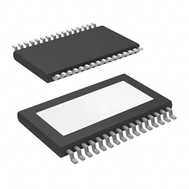
| 产品图片 |
|
| rohs | 符合RoHS含铅 / 不受限制有害物质指令(RoHS)规范要求限制 |
| 产品系列 | 音频 IC,音频放大器,Texas Instruments LM4755TSX/NOPB- |
| 数据手册 | |
| 产品型号 | LM4755TSX/NOPB |
| Pd-功率耗散 | 62.5 W |
| THD+噪声 | 0.08 % |
| 不同负载时的最大输出功率x通道数 | 11W x 2 @ 4 欧姆 |
| 产品 | Audio Amplifiers |
| 产品种类 | 音频放大器 |
| 供应商器件封装 | TO-263-9 |
| 其它名称 | LM4755TSX/NOPBDKR |
| 包装 | Digi-Reel® |
| 商标 | Texas Instruments |
| 安装类型 | 表面贴装 |
| 安装风格 | SMD/SMT |
| 封装 | Reel |
| 封装/外壳 | TO-263-10(9 引线 + 接片) |
| 封装/箱体 | TO-263-9 |
| 工作电源电压 | 9 V to 32 V |
| 工厂包装数量 | 500 |
| 最大功率耗散 | 62.5 W |
| 最大工作温度 | + 80 C |
| 最小工作温度 | - 20 C |
| 标准包装 | 1 |
| 特性 | 静音,短路和热保护 |
| 电压-电源 | 9 V ~ 32 V |
| 电源电压-最大 | 32 V |
| 电源电压-最小 | 9 V |
| 电源电流 | 10 mA |
| 电源类型 | Single |
| 类 | Class-AB |
| 类型 | Stereo |
| 系列 | LM4755 |
| 输出功率 | 11 W |
| 输出类型 | 2 通道(立体声) |

.JPG)


- 商务部:美国ITC正式对集成电路等产品启动337调查
- 曝三星4nm工艺存在良率问题 高通将骁龙8 Gen1或转产台积电
- 太阳诱电将投资9.5亿元在常州建新厂生产MLCC 预计2023年完工
- 英特尔发布欧洲新工厂建设计划 深化IDM 2.0 战略
- 台积电先进制程称霸业界 有大客户加持明年业绩稳了
- 达到5530亿美元!SIA预计今年全球半导体销售额将创下新高
- 英特尔拟将自动驾驶子公司Mobileye上市 估值或超500亿美元
- 三星加码芯片和SET,合并消费电子和移动部门,撤换高东真等 CEO
- 三星电子宣布重大人事变动 还合并消费电子和移动部门
- 海关总署:前11个月进口集成电路产品价值2.52万亿元 增长14.8%


PDF Datasheet 数据手册内容提取
LM4755 www.ti.com SNAS010E–FEBRUARY1999–REVISEDAPRIL2013 LM4755 Stereo 11W Audio Power Amplifier with Mute CheckforSamples:LM4755 FEATURES DESCRIPTION 1 • Drives4Ω and8Ω Loads The LM4755 is a stereo audio amplifier capable of 2 delivering 11W per channel of continuous average • IntegratedMuteFunction output power to a 4Ω load or 7W per channel into 8Ω • InternalGainResistors using a single 24V supply at 10% THD+N. The • MinimalExternalComponentsNeeded internalmutecircuitandpre-setgainresistorsprovide foraveryeconomicaldesignsolution. • SingleSupplyOperation • InternalCurrentLimitingandThermal Output power specifications at both 20V and 24V supplies and low external component count offer high Protection value to consumer electronic manufacturers for • Compact9-leadTO-220Package stereo TV and compact stereo applications. The • WideSupplyRange9V-40V LM4755 is specifically designed for single supply operation. APPLICATIONS • StereosTVs • CompactStereos • MiniComponentStereos KEY SPECIFICATIONS • OutputPowerat10%THDwith1kHzinto4Ω at V =24V11W(typ) CC • OutputPowerat10%THDwith1kHzinto8Ω at V =24V7W(typ) CC • ClosedLoopGain34dB(typ) • P at10%THD+N@1kHzinto4Ω Single- O EndedDDPAKPackageatV =12V2.5W(typ) CC • P at10%THD+N@1kHzinto8Ω Bridged O DDPAKPackageatV =12V5W(typ) CC 1 Pleasebeawarethatanimportantnoticeconcerningavailability,standardwarranty,anduseincriticalapplicationsof TexasInstrumentssemiconductorproductsanddisclaimerstheretoappearsattheendofthisdatasheet. Alltrademarksarethepropertyoftheirrespectiveowners. 2 PRODUCTIONDATAinformationiscurrentasofpublicationdate. Copyright©1999–2013,TexasInstrumentsIncorporated Products conform to specifications per the terms of the Texas Instruments standard warranty. Production processing does not necessarilyincludetestingofallparameters.
LM4755 SNAS010E–FEBRUARY1999–REVISEDAPRIL2013 www.ti.com TYPICAL APPLICATION Figure1. TypicalAudioAmplifierApplicationCircuit Connection Diagram 9PinTO-220 PlasticPackage(TopView) SeePackageNumberNEC 9PinDDPAK PlasticPackage(TopView) SeePackageNumberKTW 2 SubmitDocumentationFeedback Copyright©1999–2013,TexasInstrumentsIncorporated ProductFolderLinks:LM4755
LM4755 www.ti.com SNAS010E–FEBRUARY1999–REVISEDAPRIL2013 Thesedeviceshavelimitedbuilt-inESDprotection.Theleadsshouldbeshortedtogetherorthedeviceplacedinconductivefoam duringstorageorhandlingtopreventelectrostaticdamagetotheMOSgates. ABSOLUTE MAXIMUM RATINGS(1)(2)(3)(4) SupplyVoltage 40V InputVoltage ±0.7V InputVoltageatOutputPins (5) GND-0.4V OutputCurrent InternallyLimited PowerDissipation (6) 62.5W ESDSusceptibility (7) 2kV JunctionTemperature 150°C SolderingInformation NECPackage(10seconds) 250°C StorageTemperature −40°Cto150°C (1) AbsoluteMaximumRatingsindicatelimitsbeyondwhichdamagetothedevicemayoccur.OperatingRatingsindicateconditionsfor whichthedeviceisfunctional,butdonotensurespecificperformancelimits.ElectricalCharacteristicsstateDCandACelectrical specificationsunderparticulartestconditionswhichensurespecificperformancelimits.Thisassumesthatthedeviceiswithinthe OperatingRatings.Specificationsarenotensuredforparameterswherenolimitisgiven,however,thetypicalvalueisagoodindication ofdeviceperformance. (2) IfMilitary/Aerospacespecifieddevicesarerequired,pleasecontacttheTexasInstrumentsSalesOffice/Distributorsforavailabilityand specifications. (3) TheTO-263PackageisnotrecommendedforV >16Vduetoimpracticalheatsinkinglimitations. S (4) AllvoltagesaremeasuredwithrespecttotheGNDpin(5),unlessotherwsespecified. (5) TheoutputsoftheLM4755cannotbedrivenexternallyinanymodewithavoltagelowerthan-0.4VbelowGNDorpermanentdamage totheLM4755willresult. (6) Foroperatingatcasetemperaturesabove25°C,thedevicemustbederatedbasedona150°Cmaximumjunctiontemperatureanda thermalresistanceofθ =2°C/W(junctiontocase).RefertothesectionDETERMININGMAXIMUMPOWERDISSIPATIONinthe JC APPLICATIONINFORMATIONsectionformoreinformation. (7) Humanbodymodel,100pFdischargedthrougha1.5kΩresistor. OPERATING RATINGS TemperatureRangeT ≤T ≤T −40°C≤T ≤+85°C MIN A MAX A SupplyVoltage 9Vto32V θ 2°C/W JC θ 76°C/W JA ELECTRICAL CHARACTERISTICS ThefollowingspecificationsapplytoeachchannelwithV =24V,T =25°Cunlessotherwisespecified. CC A LM4755 Units Symbol Parameter Conditions Typical(1) Limit (Limits) I TotalQuiescentPower MuteOff 10 15 mA(max) TOTAL SupplyCurrent 7 mA(min) MuteOn 7 mA P OutputPower(Continuous f=1kHz,THD+N=10%,R =8Ω 7 W O L AverageperChannel) f=1kHz,THD+N=10%,R =4Ω 11 10 W(min) L V =20V,R =8Ω 4 W S L V =20V,R =4Ω 7 W S L f=1kHz,THD+N=10%,R =4Ω L 2.5 W V =12V,DDPAKPkg. S THD TotalHarmonicDistortion f=1kHz,P =1W/ch,R =8Ω 0.08 % O L V OutputSwing P =10W,R =8Ω 15 V OSW O L P =10W,R =4Ω 14 V O L X ChannelSeparation SeeApps.Circuit(Figure1) 55 dB TALK f=1kHz,V =4Vrms O (1) Typicalsaremeasuredat25°Candrepresenttheparametricnorm. Copyright©1999–2013,TexasInstrumentsIncorporated SubmitDocumentationFeedback 3 ProductFolderLinks:LM4755
LM4755 SNAS010E–FEBRUARY1999–REVISEDAPRIL2013 www.ti.com ELECTRICAL CHARACTERISTICS (continued) ThefollowingspecificationsapplytoeachchannelwithV =24V,T =25°Cunlessotherwisespecified. CC A LM4755 Units Symbol Parameter Conditions Typical(1) Limit (Limits) PSRR PowerSupplyRejectionRatio SeeApps.Circuit(Figure1) 50 dB f=120Hz,V =1mVrms O V DifferentialDCOutputOffset V =0V 0.09 0.4 V(max) ODV IN Voltage SR SlewRate 2 V/µs R InputImpedance 83 kΩ IN PBW PowerBandwidth 3dBBWatP =2.5W,R =8Ω 65 kHz O L A ClosedLoopGain(InternallySet) R =8Ω 34 33 dB(min) VCL L 35 dB(max) ε Noise IHF-AWeightingFilter,R =8Ω 0.2 mVrms IN L OutputReferred I OutputShortCircuitLimit V =0.5V,R =2Ω 2 A(min) O IN L MutePin MuteLowInputVoltage NotinMuteMode 0.8 V(max) V IL V MuteHighInputVoltage InMuteMode 2.0 2.5 V(min) IH A MuteAttenuation V =5.0V 80 dB M MUTE EQUIVALENT SCHEMATIC Figure2. 4 SubmitDocumentationFeedback Copyright©1999–2013,TexasInstrumentsIncorporated ProductFolderLinks:LM4755
LM4755 www.ti.com SNAS010E–FEBRUARY1999–REVISEDAPRIL2013 TEST CIRCUIT Figure3. TestCircuit Copyright©1999–2013,TexasInstrumentsIncorporated SubmitDocumentationFeedback 5 ProductFolderLinks:LM4755
LM4755 SNAS010E–FEBRUARY1999–REVISEDAPRIL2013 www.ti.com SYSTEM APPLICATION CIRCUIT Figure4. CircuitforExternalComponentsDescription EXTERNAL COMPONENTS DESCRIPTION Components FunctionDescription 1,2 C Providespowersupplyfilteringandbypassing. S 3,4 R WorkswithC tostabilizetheoutputstagefromhighfrequencyoscillations. SN SN 5,6 C WorkswithR tostabilizetheoutputstagefromhighfrequencyoscillations. SN SN 7 C Providesfilteringfortheinternallygeneratedhalf-supplybiasgenerator. b 8,9 C InputACcouplingcapacitorwhichblocksDCvoltageattheamplifier'sinputterminals.Alsocreatesahighpass i filterwithfc=1/(2•π•Rin•Cin). 10,11 C OutputACcouplingcapacitorwhichblocksDCvoltageattheamplifier'soutputterminal.Createsahighpassfilter o withfc=1/(2•π•Rout•Cout). 12,13 R Voltagecontrol-limitsthevoltagelevelallowedtotheamplifier'sinputterminals. i 14 R WorkswithC toprovidemutefunctiontiming. m m 15 C WorkswithR toprovidemutefunctiontiming. m m 6 SubmitDocumentationFeedback Copyright©1999–2013,TexasInstrumentsIncorporated ProductFolderLinks:LM4755
LM4755 www.ti.com SNAS010E–FEBRUARY1999–REVISEDAPRIL2013 TYPICAL PERFORMANCE CHARACTERISTICS Typicalsaremeasuredat25°Candrepresenttheparametricnorm. THD+NvsOutputPower THD+NvsOutputPower Figure5. Figure6. THD+NvsOutputPower THD+NvsOutputPower Figure7. Figure8. THD+NvsOutputPower THD+NvsOutputPower Figure9. Figure10. Copyright©1999–2013,TexasInstrumentsIncorporated SubmitDocumentationFeedback 7 ProductFolderLinks:LM4755
LM4755 SNAS010E–FEBRUARY1999–REVISEDAPRIL2013 www.ti.com TYPICAL PERFORMANCE CHARACTERISTICS (continued) Typicalsaremeasuredat25°Candrepresenttheparametricnorm. THD+NvsOutputPower THD+NvsOutputPower Figure11. Figure12. THD+NvsOutputPower THD+NvsOutputPower Figure13. Figure14. THD+NvsOutputPower THD+NvsOutputPower Figure15. Figure16. 8 SubmitDocumentationFeedback Copyright©1999–2013,TexasInstrumentsIncorporated ProductFolderLinks:LM4755
LM4755 www.ti.com SNAS010E–FEBRUARY1999–REVISEDAPRIL2013 TYPICAL PERFORMANCE CHARACTERISTICS (continued) Typicalsaremeasuredat25°Candrepresenttheparametricnorm. THD+NvsOutputPower THD+NvsOutputPower Figure17. Figure18. THD+NvsOutputPower THD+NvsOutputPower Figure19. Figure20. THD+NvsOutputPower THD+NvsOutputPower Figure21. Figure22. Copyright©1999–2013,TexasInstrumentsIncorporated SubmitDocumentationFeedback 9 ProductFolderLinks:LM4755
LM4755 SNAS010E–FEBRUARY1999–REVISEDAPRIL2013 www.ti.com TYPICAL PERFORMANCE CHARACTERISTICS (continued) Typicalsaremeasuredat25°Candrepresenttheparametricnorm. THD+NvsOutputPower THD+NvsOutputPower Figure23. Figure24. THD+NvsOutputPower THD+NvsOutputPower Figure25. Figure26. THD+NvsOutputPower THD+NvsOutputPower Figure27. Figure28. 10 SubmitDocumentationFeedback Copyright©1999–2013,TexasInstrumentsIncorporated ProductFolderLinks:LM4755
LM4755 www.ti.com SNAS010E–FEBRUARY1999–REVISEDAPRIL2013 TYPICAL PERFORMANCE CHARACTERISTICS (continued) Typicalsaremeasuredat25°Candrepresenttheparametricnorm. OutputPowervsSupplyVoltage OutputPowervsSupplyVoltage Figure29. Figure30. FrequencyResponse THD+NvsFrequency Figure31. Figure32. THD+NvsFrequency FrequencyResponse Figure33. Figure34. Copyright©1999–2013,TexasInstrumentsIncorporated SubmitDocumentationFeedback 11 ProductFolderLinks:LM4755
LM4755 SNAS010E–FEBRUARY1999–REVISEDAPRIL2013 www.ti.com TYPICAL PERFORMANCE CHARACTERISTICS (continued) Typicalsaremeasuredat25°Candrepresenttheparametricnorm. ChannelSeparation PSRRvsFrequency Figure35. Figure36. SupplyCurrentvsSupplyVoltage PowerDeratingCurve Figure37. Figure38. PowerDissipationvsOutputPower PowerDissipationvsOutputPower Figure39. Figure40. 12 SubmitDocumentationFeedback Copyright©1999–2013,TexasInstrumentsIncorporated ProductFolderLinks:LM4755
LM4755 www.ti.com SNAS010E–FEBRUARY1999–REVISEDAPRIL2013 TYPICAL PERFORMANCE CHARACTERISTICS (continued) Typicalsaremeasuredat25°Candrepresenttheparametricnorm. PowerDissipationvsOutputPower PowerDissipationvsOutputPower Figure41. Figure42. Copyright©1999–2013,TexasInstrumentsIncorporated SubmitDocumentationFeedback 13 ProductFolderLinks:LM4755
LM4755 SNAS010E–FEBRUARY1999–REVISEDAPRIL2013 www.ti.com APPLICATION INFORMATION The LM4755 contains circuitry to pull down the bias line internally, effectively shutting down the input stage. An external R-C should be used to adjust the timing of the pull-down. If the bias line is pulled down too quickly, currents induced in the internal bias resistors will cause a momentary DC voltage to appear across the inputs of each amplifier's internal differential pair, resulting in an output DC shift towards Vsupply. An R-C timing circuit shouldbeusedtolimitthepull-downtimesuchthatoutput“pops”andsignalfeedthroughswillbeminimized.The pull-down timing is a function of a number of factors, including the internal mute circuitry, the voltage used to activate the mute, the bias capacitor, the half-supply voltage, and internal resistances used in the half-supply generator.Table1showsalistofrecommendedvaluesfortheexternalR-C. Table1.RECOMMENDEDVALUESFORMUTECIRCUIT V V Rm Cm MUTE CC 5V 12V 18kΩ 10µF 5V 15V 18kΩ 10µF 5V 20V 12kΩ 10µF 5V 24V 12kΩ 10µF 5V 28V 8.2kΩ 10µF 5V 30V 8.2kΩ 10µF CAPACITORSELECTIONANDFREQUENCYRESPONSE With the LM4755, as in all single supply amplifiers, AC coupling capacitors are used to isolate the DC voltage present at the inputs (pins 3, 7) and outputs (pins 1, 8). As mentioned earlier in the EXTERNAL COMPONENTS DESCRIPTION section these capacitors create high-pass filters with their corresponding input/output impedances. The Typical Application Circuit shown in Figure 1 shows input and output capacitors of 0.1 µF and 1,000 µF respectively. At the input, with an 83 kΩ typical input resistance, the result is a high pass 3 dB point occurring at 19 Hz. There is another high pass filter at 39.8 Hz created with the output load resistance of 4Ω. Careful selection of these components is necessary to ensure that the desired frequency response is obtained. The Frequency Response curves in the TYPICAL PERFORMANCE CHARACTERISTICS section show how differentoutputcouplingcapacitorsaffectthelowfrequencyroll-off. OPERATINGINBRIDGE-MODE Though designed for use as a single-ended amplifier, the LM4755 can be used to drive a load differentially (bridge-mode). Due to the low pin count of the package, only the non-inverting inputs are available. An inverted signal must be provided to one of the inputs. This can easily be done with the use of an inexpensive op-amp configured as a standard inverting amplifier. An LF353 is a good low-cost choice. Care must be taken, however, for a bridge-mode amplifier must theoretically dissipate four times the power of a single-ended type. The load seen by each amplifier is effectively half that of the actual load being used, thus an amplifier designed to drive a 4Ω loadinsingle-endedmodeshoulddrivean8Ω loadwhenoperatinginbridge-mode. 14 SubmitDocumentationFeedback Copyright©1999–2013,TexasInstrumentsIncorporated ProductFolderLinks:LM4755
LM4755 www.ti.com SNAS010E–FEBRUARY1999–REVISEDAPRIL2013 Figure43. Bridge-ModeApplication Figure44. THD+NvsP forBridge-ModeApplication OUT Copyright©1999–2013,TexasInstrumentsIncorporated SubmitDocumentationFeedback 15 ProductFolderLinks:LM4755
LM4755 SNAS010E–FEBRUARY1999–REVISEDAPRIL2013 www.ti.com PREVENTINGOSCILLATIONS With the integration of the feedback and bias resistors on-chip, the LM4755 fits into a very compact package. However, due to the close proximity of the non-inverting input pins to the corresponding output pins, the inputs shouldbeACterminatedatalltimes.Iftheinputsareleftfloating,theamplifierwillhaveapositivefeedbackpath through high impedance coupling, resulting in a high frequency oscillation. In most applications, this termination is typically provided by the previous stage's source impedance. If the application will require an external signal, the inputs should be terminated to ground with a resistance of 50 kΩ or less on the AC side of the input coupling capacitors. UNDERVOLTAGESHUTDOWN If the power supply voltage drops below the minimum operating supply voltage, the internal under-voltage detection circuitry pulls down the half-supply bias line, shutting down the preamp section of the LM4755. Due to the wide operating supply range of the LM4755, the threshold is set to just under 9V. There may be certain applications where a higher threshold voltage is desired. One example is a design requiring a high operating supply voltage, with large supply and bias capacitors, and there is little or no other circuitry connected to the main power supply rail. In this circuit, when the power is disconnected, the supply and bias capacitors will discharge at a slower rate, possibly resulting in audible output distortion as the decaying voltage begins to clip theoutputsignal.Anexternalcircuitmaybeusedtosenseforthedesiredthreshold,andpullthebiasline(pin6) to ground to disable the input preamp. Figure 45 shows an example of such a circuit. When the voltage across the zener diode drops below its threshold, current flow into the base of Q1 is interrupted. Q2 then turns on, discharging the bias capacitor. This discharge rate is governed by several factors, including the bias capacitor value, the bias voltage, and the resistor at the emitter of Q2. An equation for approximating the value of the emitterdischargeresistor,R,isgivenbelow: R=(0.7v)/(Cb•(V /2)/0.1s) (1) CC Note that this is only a linearized approximation based on a discharge time of 0.1s. The circuit should be evaluatedandadjustedforeachapplication. As mentioned earlier in the Built-in Mute Circuit section, when using an external circuit to pull down the bias line, the rate of discharge will have an effect on the turn-off induced distortions. Please refer to the Table 1 section for moreinformation. Figure45. ExternalUndervoltagePull-Down THERMALCONSIDERATIONS HeatSinking Proper heatsinking is necessary to ensure that the amplifier will function correctly under all operating conditions. A heatsink that is too small will cause the die to heat excessively and will result in a degraded output signal as thethermalprotectioncircuitrybeginstooperate. 16 SubmitDocumentationFeedback Copyright©1999–2013,TexasInstrumentsIncorporated ProductFolderLinks:LM4755
LM4755 www.ti.com SNAS010E–FEBRUARY1999–REVISEDAPRIL2013 The choice of a heatsink for a given application is dictated by several factors: the maximum power the IC needs to dissipate, the worst-case ambient temperature of the circuit, the junction-to-case thermal resistance, and the maximum junction temperature of the IC. The heat flow approximation equation used in determining the correct heatsinkmaximumthermalresistanceisgivenbelow: T–T =P •(θ +θ +θ ) J A DMAX JC CS SA where • P =maximumpowerdissipationoftheIC DMAX • T(°C)=junctiontemperatureoftheIC J • T (°C)=ambienttemperature A • θ (°C/W)=junction-to-casethermalresistanceoftheIC JC • θ (°C/W)=case-to-heatsinkthermalresistance(typically0.2to0.5°C/W) CS • θ (°C/W)=thermalresistanceofheatsink (2) SA Whendeterminingtheproperheatsink,theaboveequationshouldbere-writtenas: θ ≤[(T–T )/P ]-θ –θ (3) SA J A DMAX JC CS DDPAKHEATSINKING Surface mount applications will be limited by the thermal dissipation properties of printed circuit board area. The DDPAK package is not recommended for surface mount applications with V > 16V due to limited printed circuit S board area. There are DDPAK package enhancements, such as clip-on heatsinks and heatsinks with adhesives, thatcanbeusedtoimproveperformance. StandardFR-4single-sidedcoppercladwillhaveanapproximateThermalresistance(θ )rangingfrom: SA 1.5×1.5in.sq. 20–27°C/W (T =28°C,Sinewave A testing,1oz.Copper) 2× 2in.sq. 16–23°C/W The above values for θ vary widely due to dimensional proportions (i.e. variations in width and length will vary SA θ ). SA For audio applications, where peak power levels are short in duration, this part will perform satisfactory with less heatsinking/copper clad area. As with any high power design proper bench testing should be undertaken to assure the design can dissipate the required power. Proper bench testing requires attention to worst case ambient temperature and air flow. At high power dissipation levels the part will show a tendency to increase saturationvoltages,thuslimitingtheundistortedpowerlevels. DETERMININGMAXIMUMPOWERDISSIPATION For a single-ended class AB power amplifier, the theoretical maximum power dissipation point is a function of the supplyvoltage,V ,andtheloadresistance,R andisgivenbythefollowingequation: S L (singlechannel) P (W)=[V 2/(2•π2•R )] DMAX S L The above equation is for a single channel class-AB power amplifier. For dual amplifiers such as the LM4755, theequationforcalculatingthetotalmaximumpowerdissipatedis: (dualchannel) P (W)=2•[V 2/(2•π2•R )] DMAX S L or V 2/(π2•R ) S L (BridgedOutputs) P (W)=4[V 2/(2π2•R )] DMAX S L Copyright©1999–2013,TexasInstrumentsIncorporated SubmitDocumentationFeedback 17 ProductFolderLinks:LM4755
LM4755 SNAS010E–FEBRUARY1999–REVISEDAPRIL2013 www.ti.com HEATSINKDESIGNEXAMPLE Determinethesystemparameters: V =24V OperatingSupplyVoltage S R =4Ω MinimumLoadImpedance L T =55°C WorstCaseAmbientTemperature A Deviceparametersfromthedatasheet: T =150°C MaximumJunctionTemperature J θ =2°C/W Junction-to-CaseThermalResistance JC Calculations: 2•P =2•[V 2/2 •π2•R )]=(24V)2/(2•π2•4Ω)=14.6W DMAX S L θ ≤ [(T -T )/P ]-θ –θ =[(150°C-55°C)/14.6W]-2°C/W–0.2°C/W=4.3°C/W SA J A DMAX JC CS Conclusion:Chooseaheatsinkwithθ ≤ 4.3°C/W. SA DDPAKHEATSINKDESIGNEXAMPLES Example1:(StereoSingle-EndedOutput) Given: T =30°C A T =150°C J R =4Ω L V =12V S θ =2°C/W JC P fromP vsP Graph: DMAX D O P ≈3.7W (4) DMAX CalculatingP : DMAX P =V 2/(π2R )=(12V)2/π2(4Ω))=3.65W (5) DMAX CC L CalculatingHeatsinkThermalResistance: θ <T −T /P −θ −θ (6) SA J A DMAX JC CS θ <120°C/3.7W−2.0°C/W−0.2°C/W=30.2°C/W (7) SA Thereforetherecommendationistouse1.5×1.5squareinchofsingle-sidedcopperclad. Example2:(StereoSingle-EndedOutput) Given: T =50°C A T =150°C J R =4Ω L V =12V S θ =2°C/W JC P fromP vsP Graph: DMAX D O P ≈3.7W (8) DMAX CalculatingP : DMAX P =V 2/(π2R )=(12V)2/(π2(4Ω))=3.65W (9) DMAX CC L CalculatingHeatsinkThermalResistance: θ <[(T −T )/P ]−θ −θ (10) SA J A DMAX JC CS 18 SubmitDocumentationFeedback Copyright©1999–2013,TexasInstrumentsIncorporated ProductFolderLinks:LM4755
LM4755 www.ti.com SNAS010E–FEBRUARY1999–REVISEDAPRIL2013 θ <100°C/3.7W−2.0°C/W−0.2°C/W=24.8°C/W (11) SA Thereforetherecommendationistouse2.0×2.0squareinchofsingle-sidedcopperclad. Example3:(BridgedOutput) Given: T =50°C A T =150°C J R =8Ω L V =12V S θ =2°C/W JC CalculatingP : DMAX P =4[V 2/(2π2R )]=4(12V)2/(2π2(8Ω))=3.65W (12) DMAX CC L CalculatingHeatsinkThermalResistance: θ <[(T −T )/P ]−θ −θ (13) SA J A DMAX JC CS θ <100°C/3.7W−2.0°C/W−0.2°C/W=24.8°C/W (14) SA Thereforetherecommendationistouse2.0×2.0squareinchofsingle-sidedcopperclad. LAYOUTANDGROUNDRETURNS Proper PC board layout is essential for good circuit performance. When laying out a PC board for an audio power amplifier, particular attention must be paid to the routing of the output signal ground returns relative to the input signal and bias capacitor grounds. To prevent any ground loops, the ground returns for the output signals should be routed separately and brought together at the supply ground. The input signal grounds and the bias capacitor ground line should also be routed separately. The 0.1 µF high frequency supply bypass capacitor shouldbeplacedascloseaspossibletotheIC. Copyright©1999–2013,TexasInstrumentsIncorporated SubmitDocumentationFeedback 19 ProductFolderLinks:LM4755
LM4755 SNAS010E–FEBRUARY1999–REVISEDAPRIL2013 www.ti.com PCBOARDLAYOUT-COMPOSITE Figure46. 20 SubmitDocumentationFeedback Copyright©1999–2013,TexasInstrumentsIncorporated ProductFolderLinks:LM4755
LM4755 www.ti.com SNAS010E–FEBRUARY1999–REVISEDAPRIL2013 PCBOARDLAYOUT-SILKSCREEN Figure47. Copyright©1999–2013,TexasInstrumentsIncorporated SubmitDocumentationFeedback 21 ProductFolderLinks:LM4755
LM4755 SNAS010E–FEBRUARY1999–REVISEDAPRIL2013 www.ti.com PCBOARDLAYOUT-SOLDERSIDE Figure48. 22 SubmitDocumentationFeedback Copyright©1999–2013,TexasInstrumentsIncorporated ProductFolderLinks:LM4755
LM4755 www.ti.com SNAS010E–FEBRUARY1999–REVISEDAPRIL2013 REVISION HISTORY ChangesfromRevisionD(April2013)toRevisionE Page • ChangedlayoutofNationalDataSheettoTIformat.......................................................................................................... 22 Copyright©1999–2013,TexasInstrumentsIncorporated SubmitDocumentationFeedback 23 ProductFolderLinks:LM4755
PACKAGE OPTION ADDENDUM www.ti.com 6-Feb-2020 PACKAGING INFORMATION Orderable Device Status Package Type Package Pins Package Eco Plan Lead/Ball Finish MSL Peak Temp Op Temp (°C) Device Marking Samples (1) Drawing Qty (2) (6) (3) (4/5) LM4755TSX/NOPB ACTIVE DDPAK/ KTW 9 500 Pb-Free (RoHS SN Level-3-245C-168 HR -20 to 80 LM4755TS TO-263 Exempt) (1) The marketing status values are defined as follows: ACTIVE: Product device recommended for new designs. LIFEBUY: TI has announced that the device will be discontinued, and a lifetime-buy period is in effect. NRND: Not recommended for new designs. Device is in production to support existing customers, but TI does not recommend using this part in a new design. PREVIEW: Device has been announced but is not in production. Samples may or may not be available. OBSOLETE: TI has discontinued the production of the device. (2) RoHS: TI defines "RoHS" to mean semiconductor products that are compliant with the current EU RoHS requirements for all 10 RoHS substances, including the requirement that RoHS substance do not exceed 0.1% by weight in homogeneous materials. Where designed to be soldered at high temperatures, "RoHS" products are suitable for use in specified lead-free processes. TI may reference these types of products as "Pb-Free". RoHS Exempt: TI defines "RoHS Exempt" to mean products that contain lead but are compliant with EU RoHS pursuant to a specific EU RoHS exemption. Green: TI defines "Green" to mean the content of Chlorine (Cl) and Bromine (Br) based flame retardants meet JS709B low halogen requirements of <=1000ppm threshold. Antimony trioxide based flame retardants must also meet the <=1000ppm threshold requirement. (3) MSL, Peak Temp. - The Moisture Sensitivity Level rating according to the JEDEC industry standard classifications, and peak solder temperature. (4) There may be additional marking, which relates to the logo, the lot trace code information, or the environmental category on the device. (5) Multiple Device Markings will be inside parentheses. Only one Device Marking contained in parentheses and separated by a "~" will appear on a device. If a line is indented then it is a continuation of the previous line and the two combined represent the entire Device Marking for that device. (6) Lead/Ball Finish - Orderable Devices may have multiple material finish options. Finish options are separated by a vertical ruled line. Lead/Ball Finish values may wrap to two lines if the finish value exceeds the maximum column width. Important Information and Disclaimer:The information provided on this page represents TI's knowledge and belief as of the date that it is provided. TI bases its knowledge and belief on information provided by third parties, and makes no representation or warranty as to the accuracy of such information. Efforts are underway to better integrate information from third parties. TI has taken and continues to take reasonable steps to provide representative and accurate information but may not have conducted destructive testing or chemical analysis on incoming materials and chemicals. TI and TI suppliers consider certain information to be proprietary, and thus CAS numbers and other limited information may not be available for release. In no event shall TI's liability arising out of such information exceed the total purchase price of the TI part(s) at issue in this document sold by TI to Customer on an annual basis. Addendum-Page 1
PACKAGE MATERIALS INFORMATION www.ti.com 8-Nov-2013 TAPE AND REEL INFORMATION *Alldimensionsarenominal Device Package Package Pins SPQ Reel Reel A0 B0 K0 P1 W Pin1 Type Drawing Diameter Width (mm) (mm) (mm) (mm) (mm) Quadrant (mm) W1(mm) LM4755TSX/NOPB DDPAK/ KTW 9 500 330.0 24.4 10.75 14.85 5.0 16.0 24.0 Q2 TO-263 PackMaterials-Page1
PACKAGE MATERIALS INFORMATION www.ti.com 8-Nov-2013 *Alldimensionsarenominal Device PackageType PackageDrawing Pins SPQ Length(mm) Width(mm) Height(mm) LM4755TSX/NOPB DDPAK/TO-263 KTW 9 500 367.0 367.0 45.0 PackMaterials-Page2
MECHANICAL DATA KTW0009A TS9A (Rev B) BOTTOM SIDE OF PACKAGE www.ti.com
IMPORTANTNOTICEANDDISCLAIMER TI PROVIDES TECHNICAL AND RELIABILITY DATA (INCLUDING DATASHEETS), DESIGN RESOURCES (INCLUDING REFERENCE DESIGNS), APPLICATION OR OTHER DESIGN ADVICE, WEB TOOLS, SAFETY INFORMATION, AND OTHER RESOURCES “AS IS” AND WITH ALL FAULTS, AND DISCLAIMS ALL WARRANTIES, EXPRESS AND IMPLIED, INCLUDING WITHOUT LIMITATION ANY IMPLIED WARRANTIES OF MERCHANTABILITY, FITNESS FOR A PARTICULAR PURPOSE OR NON-INFRINGEMENT OF THIRD PARTY INTELLECTUAL PROPERTY RIGHTS. These resources are intended for skilled developers designing with TI products. You are solely responsible for (1) selecting the appropriate TI products for your application, (2) designing, validating and testing your application, and (3) ensuring your application meets applicable standards, and any other safety, security, or other requirements. These resources are subject to change without notice. TI grants you permission to use these resources only for development of an application that uses the TI products described in the resource. Other reproduction and display of these resources is prohibited. No license is granted to any other TI intellectual property right or to any third party intellectual property right. TI disclaims responsibility for, and you will fully indemnify TI and its representatives against, any claims, damages, costs, losses, and liabilities arising out of your use of these resources. TI’s products are provided subject to TI’s Terms of Sale (www.ti.com/legal/termsofsale.html) or other applicable terms available either on ti.com or provided in conjunction with such TI products. TI’s provision of these resources does not expand or otherwise alter TI’s applicable warranties or warranty disclaimers for TI products. Mailing Address: Texas Instruments, Post Office Box 655303, Dallas, Texas 75265 Copyright © 2020, Texas Instruments Incorporated