ICGOO在线商城 > 集成电路(IC) > PMIC - 电压基准 > LM4040D10IDCKR
 Datasheet下载
- 型号: LM4040D10IDCKR
- 制造商: Texas Instruments
- 库位|库存: xxxx|xxxx
- 要求:
| 数量阶梯 | 香港交货 | 国内含税 |
| +xxxx | $xxxx | ¥xxxx |
查看当月历史价格
查看今年历史价格
LM4040D10IDCKR产品简介:
ICGOO电子元器件商城为您提供LM4040D10IDCKR由Texas Instruments设计生产,在icgoo商城现货销售,并且可以通过原厂、代理商等渠道进行代购。 LM4040D10IDCKR价格参考¥1.89-¥4.67。Texas InstrumentsLM4040D10IDCKR封装/规格:PMIC - 电压基准, 分流器 电压基准 IC ±1% 15mA SC-70-5。您可以下载LM4040D10IDCKR参考资料、Datasheet数据手册功能说明书,资料中有LM4040D10IDCKR 详细功能的应用电路图电压和使用方法及教程。
LM4040D10IDCKR 是 Texas Instruments(德州仪器)生产的一款精密电压基准芯片,属于 PMIC(电源管理集成电路)中的电压基准类别。该器件提供高精度、低温度漂移的基准电压输出,广泛应用于需要稳定参考电压的电子系统中。

其典型应用场景包括:

1. 模数转换器(ADC)和数模转换器(DAC)参考电压源:为高精度数据转换器提供稳定的参考电压,确保转换精度不受电源波动影响。

2. 电源管理系统:在电池供电设备、DC-DC转换器和LDO稳压器中作为电压监控或调节的基准,提高系统稳定性与精度。

3. 测试与测量设备:如万用表、示波器等精密仪器中,用于提供高稳定性的电压基准以保证测量准确性。

4. 工业控制系统:在PLC(可编程逻辑控制器)、传感器模块中作为参考电压源,提升系统抗干扰能力和长期稳定性。

5. 通信设备:用于基站、光模块等设备中的电源监控和信号调理电路中,保障通信质量。

该器件采用SOT23-5封装,具备低功耗、小体积特点,适合空间受限的便携式设备应用。由于其出色的温度稳定性和长期可靠性,LM4040D10IDCKR 在工业级和高精度要求的应用中被广泛采用。
| 参数 | 数值 |
| 产品目录 | 集成电路 (IC) |
| 描述 | IC VREF SHUNT PREC 10V SC-70-5 |
| 产品分类 | |
| 品牌 | Texas Instruments |
| 数据手册 | |
| 产品图片 |
|
| 产品型号 | LM4040D10IDCKR |
| rohs | 无铅 / 符合限制有害物质指令(RoHS)规范要求 |
| 产品系列 | - |
| 产品培训模块 | http://www.digikey.cn/PTM/IndividualPTM.page?site=cn&lang=zhs&ptm=26100 |
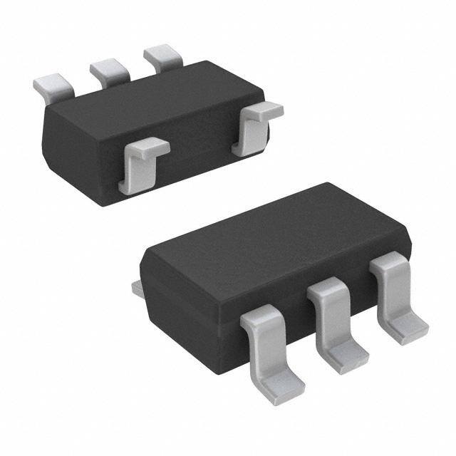
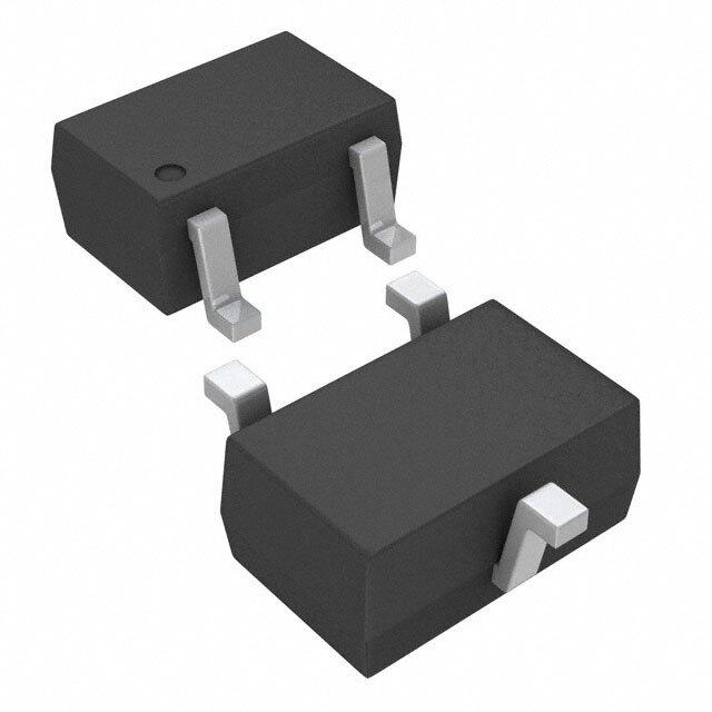
| 供应商器件封装 | SC-70-5 |
| 其它名称 | 296-20898-1 |
| 制造商产品页 | http://www.ti.com/general/docs/suppproductinfo.tsp?distId=10&orderablePartNumber=LM4040D10IDCKR |
| 包装 | 剪切带 (CT) |
| 参考类型 | 旁路,精度 |
| 安装类型 | 表面贴装 |
| 容差 | ±1% |
| 封装/外壳 | 6-TSSOP(5 引线),SC-88A,SOT-353 |
| 工作温度 | -40°C ~ 85°C |
| 标准包装 | 1 |
| 温度系数 | 150ppm/°C |
| 电压-输入 | - |
| 电压-输出 | 10V |
| 电流-输出 | 15mA |
| 电流-阴极 | 130µA |
| 电流-静态 | - |
| 通道数 | 1 |


- 商务部:美国ITC正式对集成电路等产品启动337调查
- 曝三星4nm工艺存在良率问题 高通将骁龙8 Gen1或转产台积电
- 太阳诱电将投资9.5亿元在常州建新厂生产MLCC 预计2023年完工
- 英特尔发布欧洲新工厂建设计划 深化IDM 2.0 战略
- 台积电先进制程称霸业界 有大客户加持明年业绩稳了
- 达到5530亿美元!SIA预计今年全球半导体销售额将创下新高
- 英特尔拟将自动驾驶子公司Mobileye上市 估值或超500亿美元
- 三星加码芯片和SET,合并消费电子和移动部门,撤换高东真等 CEO
- 三星电子宣布重大人事变动 还合并消费电子和移动部门
- 海关总署:前11个月进口集成电路产品价值2.52万亿元 增长14.8%


PDF Datasheet 数据手册内容提取
Product Order Technical Tools & Support & Folder Now Documents Software Community LM4040A,LM4040B LM4040C,LM4040D SLOS456N–JANUARY2005–REVISEDOCTOBER2017 LM4040 Precision Micropower Shunt Voltage Reference 1 Features 3 Description • FixedOutputVoltagesof2.048V,2.5V,3V, The LM4040 series of shunt voltage references are 1 versatile, easy-to-use references that cater to a vast 4.096V,5V,8.192V,and10V array of applications. The 2-pin fixed-output device • TightOutputTolerancesandLowTemperature requires no external capacitors for operation and is Coefficient stable with all capacitive loads. Additionally, the – Max0.1%,100ppm/°C– AGrade reference offers low dynamic impedance, low noise, and low temperature coefficient to ensure a stable – Max0.2%,100ppm/°C– BGrade output voltage over a wide range of operating – Max0.5%,100ppm/°C– CGrade currents and temperatures. The LM4040 uses fuse – Max1.0%,150ppm/°C– DGrade and Zener-zap reverse breakdown voltage trim during • LowOutputNoise:35 μV Typ wafer sort to offer four output voltage tolerances, RMS ranging from 0.1% (max) for the A grade to 1% (max) • WideOperatingCurrentRange:45μATypto15 for the D grade. Thus, a great deal of flexibility is mA offered to designers in choosing the best cost-to- • StableWithAllCapacitiveLoads;NoOutput performanceratiofortheirapplications. CapacitorRequired Packaged in space-saving SC-70 and SOT-23-3 • AvailableinExtendedTemperatureRange:–40°C packages and requiring a minimum current of 45 μA to125°C (typ), the LM4040 also is ideal for portable applications. The LM4040xI is characterized for 2 Applications operation over an ambient temperature range of –40°C to 85°C. The LM4040xQ is characterized for • Data-AcquisitionSystems operation over an ambient temperature range of • PowerSuppliesandPower-SupplyMonitors –40°Cto125°C. • InstrumentationandTestEquipment DeviceInformation(1) • ProcessControls PARTNUMBER PACKAGE(PIN) BODYSIZE(NOM) • PrecisionAudio SOT-23(3) 2.92mm×1.30mm • AutomotiveElectronics LM4040 SC70(6) 2.00mm×1.25mm • EnergyManagement (1) For all available packages, see the orderable addendum at • Battery-PoweredEquipment theendofthedatasheet. SimplifiedSchematic V S R I + I S Z L I L V Z I Z LM4040 1 An IMPORTANT NOTICE at the end of this data sheet addresses availability, warranty, changes, use in safety-critical applications, intellectualpropertymattersandotherimportantdisclaimers.PRODUCTIONDATA.
LM4040A,LM4040B LM4040C,LM4040D SLOS456N–JANUARY2005–REVISEDOCTOBER2017 www.ti.com Table of Contents 1 Features.................................................................. 1 6.17 LM4040C50I,LM4040D50IElectrical Characteristics.........................................................18 2 Applications........................................................... 1 6.18 LM4040C50Q,LM4040D50QElectrical 3 Description............................................................. 1 Characteristics.........................................................19 4 RevisionHistory..................................................... 2 6.19 LM4040A82I,LM4040B82IElectrical 5 PinConfigurationandFunctions......................... 4 Characteristics.........................................................20 6 Specifications......................................................... 5 6.20 LM4040C82I,LM4040D82IElectrical Characteristics.........................................................21 6.1 AbsoluteMaximumRatings......................................5 6.21 LM4040A10I,LM4040B10IElectrical 6.2 ESDRatings..............................................................5 Characteristics.........................................................22 6.3 RecommendedOperatingConditions.......................5 6.22 LM4040C10I,LM4040D10IElectrical 6.4 ThermalInformation..................................................5 Characteristics.........................................................23 6.5 LM4040A20I,LM4040B20IElectrical 6.23 TypicalCharacteristics..........................................24 Characteristics...........................................................6 7 DetailedDescription............................................ 25 6.6 LM4040C20I,LM4040D20IElectrical Characteristics...........................................................7 7.1 Overview.................................................................25 6.7 LM4040C20Q,LM4040D20QElectrical 7.2 FunctionalBlockDiagram.......................................25 Characteristics...........................................................8 7.3 FeatureDescription.................................................25 6.8 LM4040A25I,LM4040B25IElectrical 7.4 DeviceFunctionalModes........................................25 Characteristics...........................................................9 8 ApplicationsandImplementation...................... 26 6.9 LM4040C25I,LM4040D25IElectrical 8.1 ApplicationInformation............................................26 Characteristics.........................................................10 8.2 TypicalApplications................................................26 6.10 LM4040C25Q,LM4040D25QElectrical 9 PowerSupplyRecommendations...................... 29 Characteristics.........................................................11 6.11 LM4040A30I,LM4040B30IElectrical 10 Layout................................................................... 29 Characteristics.........................................................12 10.1 LayoutGuidelines.................................................29 6.12 LM4040C30I,LM4040D30IElectrical 10.2 LayoutExample....................................................29 Characteristics.........................................................13 11 DeviceandDocumentationSupport................. 30 6.13 LM4040C30Q,LM4040D30QElectrical 11.1 RelatedLinks........................................................30 Characteristics.........................................................14 11.2 Trademarks...........................................................30 6.14 LM4040A41I,LM4040B41IElectrical 11.3 ElectrostaticDischargeCaution............................30 Characteristics.........................................................15 11.4 Glossary................................................................30 6.15 LM4040C41I,LM4040D41IElectrical Characteristics.........................................................16 12 Mechanical,Packaging,andOrderable 6.16 LM4040A50I,LM4040B50IElectrical Information........................................................... 30 Characteristics.........................................................17 4 Revision History ChangesfromRevisionM(January2015)toRevisionN Page • Changedgenericpartnumbertoincludeshorterlist(LM4040A/B/C/D)................................................................................ 1 • AddedAveragetemperaturecoefficientofreversebreakdownvoltagefootnotetoallelectricaltables................................ 6 • ChangedThermalhysteresisinelectricalcharacteristicstables............................................................................................ 6 ChangesfromRevisionL(January2009)toRevisionM Page • AddedApplications,DeviceInformationtable,PinFunctionstable,ESDRatingstable,ThermalInformationtable, FeatureDescriptionsection,DeviceFunctionalModes,ApplicationandImplementationsection,PowerSupply Recommendationssection,Layoutsection,DeviceandDocumentationSupportsection,andMechanical, Packaging,andOrderableInformationsection...................................................................................................................... 1 • DeletedOrderingInformationtable........................................................................................................................................ 1 2 SubmitDocumentationFeedback Copyright©2005–2017,TexasInstrumentsIncorporated ProductFolderLinks:LM4040A LM4040BLM4040C LM4040D
LM4040A,LM4040B LM4040C,LM4040D www.ti.com SLOS456N–JANUARY2005–REVISEDOCTOBER2017 DeviceComparisonTable(1) DEVICE ORDERABLE TA GRADE VKA PARTNUMBER 2.048V LM4040A20I Agrade: 2.5V LM4040A25I 0.1%initial 3V LM4040A30I accuracy and 4.096V LM4040A41I 100ppm/°C 5V LM4040A50I temperature coefficient 8.192V LM4040A82I 10V LM4040A10I –40°Cto85°C 2.048V LM4040B20I Bgrade: 2.5V LM4040B25I 0.2%initial 3V LM4040B30I accuracy and 4.096V LM4040B41I 100ppm/°C 5V LM4040B50I temperature coefficient 8.192V LM4040B82I 10V LM4040B10I 2.048V LM4040C20I Cgrade: 2.5V LM4040C25I 0.5%initial 3V LM4040C30I accuracy –40°Cto85°C and 4.096V LM4040C41I 100ppm/°C 5V LM4040C50I temperature coefficient 8.192V LM4040C82I 10V LM4040C10I 2.048V LM4040D20I Dgrade: 2.5V LM4040D25I 1.0%initial 3V LM4040D30I accuracy –40°Cto85°C and 4.096V LM4040D41I 150ppm/°C 5V LM4040D50I temperature coefficient 8.192V LM4040D82I 10V LM4040D10I Cgrade: 2.048V LM4040C20Q 0.5%initial 2.5V LM4040C25Q accuracy and 3V LM4040C30Q 100ppm/°C temperature 5V LM4040C50Q coefficient –40°Cto125°C Dgrade: 2.048V LM4040D20Q 1.0%initial 2.5V LM4040D25Q accuracy and 3V LM4040D30Q 150ppm/°C temperature 5V LM4040D50Q coefficient (1) Forthemostcurrentpackageandorderinginformation,seethePackageOptionAddendumattheendofthisdocument,orseetheTI websiteatwww.ti.com. Copyright©2005–2017,TexasInstrumentsIncorporated SubmitDocumentationFeedback 3 ProductFolderLinks:LM4040A LM4040BLM4040C LM4040D
LM4040A,LM4040B LM4040C,LM4040D SLOS456N–JANUARY2005–REVISEDOCTOBER2017 www.ti.com 5 Pin Configuration and Functions DBZ (SOT-23) PACKAGE (TOPVIEW) 1 CATHODE 3* 2 ANODE * Pin 3 is attached to substrate and must be connectedtoANODE or left open. DCK (SC-70) PACKAGE (TOPVIEW) 1 ANODE 5 NC NC 2 CATHODE 4 NC 3 NC–No internal connection PinFunctions PIN TYPE DESCRIPTION NAME DBZ DCK CATHODE 1 3 I/O ShuntCurrent/Voltageinput ANODE 2 1 O Commonpin,normallyconnectedtoground NC — 2,4,5 I NoInternalConnection * 3 — I SubstrateConnection 4 SubmitDocumentationFeedback Copyright©2005–2017,TexasInstrumentsIncorporated ProductFolderLinks:LM4040A LM4040BLM4040C LM4040D
LM4040A,LM4040B LM4040C,LM4040D www.ti.com SLOS456N–JANUARY2005–REVISEDOCTOBER2017 6 Specifications 6.1 Absolute Maximum Ratings overfree-airtemperaturerange(unlessotherwisenoted)(1) MIN MAX UNIT I Continuouscathodecurrent –10 25 mA Z T Operatingvirtualjunctiontemperature 150 °C J T Storagetemperaturerange –65 150 °C stg (1) StressesbeyondthoselistedunderAbsoluteMaximumRatingsmaycausepermanentdamagetothedevice.Thesearestressratings only,andfunctionaloperationofthedeviceattheseoranyotherconditionsbeyondthoseindicatedunderRecommendedOperating Conditionsisnotimplied.Exposuretoabsolute-maximum-ratedconditionsforextendedperiodsmayaffectdevicereliability. 6.2 ESD Ratings VALUE UNIT Humanbodymodel(HBM),perANSI/ESDA/JEDECJS-001,allpins(1) ±2000 V(ESD) Electrostaticdischarge Chargeddevicemodel(CDM),perJEDECspecificationJESD22-C101, ±1000 V allpins(2) (1) JEDECdocumentJEP155statesthat500-VHBMallowssafemanufacturingwithastandardESDcontrolprocess. (2) JEDECdocumentJEP157statesthat250-VCDMallowssafemanufacturingwithastandardESDcontrolprocess. 6.3 Recommended Operating Conditions MIN MAX UNIT I Cathodecurrent (1) 15 mA Z LM4040xxxI –40 85 T Free-airtemperature °C A LM4040xxxQ –40 125 (1) Seeparametrictables 6.4 Thermal Information LM4040 THERMALMETRIC(1) DBZ DCK UNIT 3PINS 5PINS R Junction-to-ambientthermalresistance 206 252 °C/W θJA (1) Formoreinformationabouttraditionalandnewthermalmetrics,seetheSemiconductorandICPackageThermalMetricsapplication report. Copyright©2005–2017,TexasInstrumentsIncorporated SubmitDocumentationFeedback 5 ProductFolderLinks:LM4040A LM4040BLM4040C LM4040D
LM4040A,LM4040B LM4040C,LM4040D SLOS456N–JANUARY2005–REVISEDOCTOBER2017 www.ti.com 6.5 LM4040A20I, LM4040B20I Electrical Characteristics atindustrialtemperaturerange,full-rangeT =–40°Cto85°C(unlessotherwisenoted) A LM4040A20I LM4040B20I PARAMETER TESTCONDITIONS T UNIT A MIN TYP MAX MIN TYP MAX V Reversebreakdownvoltage I =100μA 25°C 2.048 2.048 V Z Z Reversebreakdownvoltage 25°C –2 2 –4.1 4.1 ΔV I =100μA mV Z tolerance Z Fullrange –15 15 –17 17 25°C 45 75 45 75 I Minimumcathodecurrent μA Z,min Fullrange 80 80 I =10mA 25°C ±20 ±20 Z Averagetemperaturecoefficient 25°C ±15 ±15 α ofreversebreakdownvoltage I =1mA ppm/°C VZ Z (1) Fullrange ±100 ±100 I =100μA 25°C ±15 ±15 Z 25°C 0.3 0.8 0.3 0.8 I <I <1mA (cid:1)V Reversebreakdownvoltage Z,min Z Fullrange 1 1 Z (cid:1)IZ cchhaannggeewithcathodecurrent 25°C 2.5 6 2.5 6 mV 1mA<I <15mA Z Fullrange 8 8 I =1mA,f=120Hz, Z Reversedynamicimpedance Z 25°C 0.3 0.8 0.3 0.8 Ω Z I =0.1I AC Z I =100μA, e Widebandnoise Z 25°C 35 35 μV N 10Hz≤f≤10kHz RMS t=1000h, Long-termstabilityofreverse T =25°C±0.1°C, 120 120 ppm breakdownvoltage A I =100μA Z V Thermalhysteresis(2) ΔT =–40°Cto125°C 0.08% 0.08% — HYST A (1) TheovertemperaturelimitforReverseBreakdownVoltageToleranceisdefinedastheroomtemperatureReverseBreakdownVoltage Tolerance±[(ΔV /ΔT)(maxΔT)(V )].Where,ΔV /ΔTistheV temperaturecoefficient,maxΔTisthemaximumdifferenceintemperature R R R R fromthereferencepointof25°CtoT orT ,andV isthereversebreakdownvoltage.Thetotalovertemperaturetoleranceforthe MIN MAX R differentgradesintheindustrialtemperaturerangewheremaxΔT=65°Cisshownbelow: A-grade:±0.75%=±0.1%±100ppm/°C×65°C B-grade:±0.85%=±0.2%±100ppm/°C×65°C C-grade:±1.15%=±0.5%±100ppm/°C×65°C D-grade:±1.98%=±1.0%±150ppm/°C×65°C ThetotalovertemperaturetoleranceforthedifferentgradesintheextendedtemperaturerangewheremaxΔT=100°Cisshownbelow: C-grade:±1.5%=±0.5%±100ppm/°C×100°C D-grade:±2.5%=±1.0%±150ppm/°C×100°C Therefore,asanexample,theA-grade2.5-VLM4040hasanovertemperatureReverseBreakdownVoltagetoleranceof±2.5V×0.75% =±19mV. (2) Thermalhysteresisisdefinedasthedifferenceinvoltagemeasuredat25°Caftercyclingtotemperature–40°Candthe25°C measurementaftercyclingtotemperature125°C. 6 SubmitDocumentationFeedback Copyright©2005–2017,TexasInstrumentsIncorporated ProductFolderLinks:LM4040A LM4040BLM4040C LM4040D
LM4040A,LM4040B LM4040C,LM4040D www.ti.com SLOS456N–JANUARY2005–REVISEDOCTOBER2017 6.6 LM4040C20I, LM4040D20I Electrical Characteristics atindustrialtemperaturerange,full-rangeT =–40°Cto85°C(unlessotherwisenoted) A LM4040C20I LM4040D20I PARAMETER TESTCONDITIONS T UNIT A MIN TYP MAX MIN TYP MAX V Reversebreakdownvoltage I =100μA 25°C 2.048 2.048 V Z Z Reversebreakdownvoltage 25°C –10 10 –20 20 ΔV I =100μA mV Z tolerance Z Fullrange –23 23 –40 40 25°C 45 75 45 75 I Minimumcathodecurrent μA Z,min Fullrange 80 80 I =10mA 25°C ±20 ±20 Z Averagetemperaturecoefficient 25°C ±15 ±15 α ofreversebreakdownvoltage I =1mA ppm/°C VZ Z (1) Fullrange ±100 ±150 I =100μA 25°C ±15 ±15 Z 25°C 0.3 0.8 0.3 1 I <I <1mA (cid:1)V Reversebreakdownvoltage Z,min Z Fullrange 1 1.2 Z (cid:1)IZ cchhaannggeewithcathodecurrent 25°C 2.5 6 2.5 8 mV 1mA<I <15mA Z Fullrange 8 10 I =1mA,f=120Hz, Z Reversedynamicimpedance Z 25°C 0.3 0.9 0.3 1.1 Ω Z I =0.1I AC Z I =100μA, e Widebandnoise Z 25°C 35 35 μV N 10Hz≤f≤10kHz RMS t=1000h, Long-termstabilityofreverse T =25°C±0.1°C, 120 120 ppm breakdownvoltage A I =100μA Z V Thermalhysteresis(2) ΔT =–40°Cto125°C 0.08% 0.08% — HYST A (1) TheovertemperaturelimitforReverseBreakdownVoltageToleranceisdefinedastheroomtemperatureReverseBreakdownVoltage Tolerance±[(ΔV /ΔT)(maxΔT)(V )].Where,ΔV /ΔTistheV temperaturecoefficient,maxΔTisthemaximumdifferenceintemperature R R R R fromthereferencepointof25°CtoT orT ,andV isthereversebreakdownvoltage.Thetotalovertemperaturetoleranceforthe MIN MAX R differentgradesintheindustrialtemperaturerangewheremaxΔT=65°Cisshownbelow: A-grade:±0.75%=±0.1%±100ppm/°C×65°C B-grade:±0.85%=±0.2%±100ppm/°C×65°C C-grade:±1.15%=±0.5%±100ppm/°C×65°C D-grade:±1.98%=±1.0%±150ppm/°C×65°C ThetotalovertemperaturetoleranceforthedifferentgradesintheextendedtemperaturerangewheremaxΔT=100°Cisshownbelow: C-grade:±1.5%=±0.5%±100ppm/°C×100°C D-grade:±2.5%=±1.0%±150ppm/°C×100°C Therefore,asanexample,theA-grade2.5-VLM4040hasanovertemperatureReverseBreakdownVoltagetoleranceof±2.5V×0.75% =±19mV. (2) Thermalhysteresisisdefinedasthedifferenceinvoltagemeasuredat25°Caftercyclingtotemperature–40°Candthe25°C measurementaftercyclingtotemperature125°C. Copyright©2005–2017,TexasInstrumentsIncorporated SubmitDocumentationFeedback 7 ProductFolderLinks:LM4040A LM4040BLM4040C LM4040D
LM4040A,LM4040B LM4040C,LM4040D SLOS456N–JANUARY2005–REVISEDOCTOBER2017 www.ti.com 6.7 LM4040C20Q, LM4040D20Q Electrical Characteristics atextendedtemperaturerange,full-rangeT =–40°Cto125°C(unlessotherwisenoted) A LM4040C20Q LM4040D20Q PARAMETER TESTCONDITIONS T UNIT A MIN TYP MAX MIN TYP MAX V Reversebreakdownvoltage I =100μA 25°C 2.048 2.048 V Z Z Reversebreakdownvoltage 25°C –10 10 –20 20 ΔV I =100μA mV Z tolerance Z Fullrange –30 30 –50 50 25°C 45 75 45 75 I Minimumcathodecurrent μA Z,min Fullrange 80 80 I =10mA 25°C ±20 ±20 Z Averagetemperaturecoefficient 25°C ±15 ±15 α ofreversebreakdownvoltage I =1mA ppm/°C VZ Z (1) Fullrange ±100 ±150 I =100μA 25°C ±15 ±15 Z 25°C 0.3 0.8 0.3 1 I <I <1mA (cid:1)V Reversebreakdownvoltage Z,min Z Fullrange 1 1.2 Z (cid:1)IZ cchhaannggeewithcathodecurrent 25°C 2.5 6 2.5 8 mV 1mA<I <15mA Z Fullrange 8 10 I =1mA,f=120Hz, Z Reversedynamicimpedance Z 25°C 0.3 0.9 0.3 1.1 Ω Z I =0.1I AC Z I =100μA, e Widebandnoise Z 25°C 35 35 μV N 10Hz≤f≤10kHz RMS t=1000h, Long-termstabilityofreverse T =25°C±0.1°C, 120 120 ppm breakdownvoltage A I =100μA Z V Thermalhysteresis(2) ΔT =–40°Cto125°C 0.08% 0.08% — HYST A (1) TheovertemperaturelimitforReverseBreakdownVoltageToleranceisdefinedastheroomtemperatureReverseBreakdownVoltage Tolerance±[(ΔV /ΔT)(maxΔT)(V )].Where,ΔV /ΔTistheV temperaturecoefficient,maxΔTisthemaximumdifferenceintemperature R R R R fromthereferencepointof25°CtoT orT ,andV isthereversebreakdownvoltage.Thetotalovertemperaturetoleranceforthe MIN MAX R differentgradesintheindustrialtemperaturerangewheremaxΔT=65°Cisshownbelow: A-grade:±0.75%=±0.1%±100ppm/°C×65°C B-grade:±0.85%=±0.2%±100ppm/°C×65°C C-grade:±1.15%=±0.5%±100ppm/°C×65°C D-grade:±1.98%=±1.0%±150ppm/°C×65°C ThetotalovertemperaturetoleranceforthedifferentgradesintheextendedtemperaturerangewheremaxΔT=100°Cisshownbelow: C-grade:±1.5%=±0.5%±100ppm/°C×100°C D-grade:±2.5%=±1.0%±150ppm/°C×100°C Therefore,asanexample,theA-grade2.5-VLM4040hasanovertemperatureReverseBreakdownVoltagetoleranceof±2.5V×0.75% =±19mV. (2) Thermalhysteresisisdefinedasthedifferenceinvoltagemeasuredat25°Caftercyclingtotemperature–40°Candthe25°C measurementaftercyclingtotemperature125°C. 8 SubmitDocumentationFeedback Copyright©2005–2017,TexasInstrumentsIncorporated ProductFolderLinks:LM4040A LM4040BLM4040C LM4040D
LM4040A,LM4040B LM4040C,LM4040D www.ti.com SLOS456N–JANUARY2005–REVISEDOCTOBER2017 6.8 LM4040A25I, LM4040B25I Electrical Characteristics atindustrialtemperaturerange,full-rangeT =–40°Cto85°C(unlessotherwisenoted) A LM4040A25I LM4040B25I PARAMETER TESTCONDITIONS T UNIT A MIN TYP MAX MIN TYP MAX V Reversebreakdownvoltage I =100μA 25°C 2.5 2.5 V Z Z Reversebreakdownvoltage 25°C –2.5 2.5 –5 5 ΔV I =100μA mV Z tolerance Z Fullrange –19 19 –21 21 25°C 45 75 45 75 I Minimumcathodecurrent μA Z,min Fullrange 80 80 I =10mA 25°C ±20 ±20 Z Averagetemperaturecoefficient 25°C ±15 ±15 α ofreversebreakdownvoltage I =1mA ppm/°C VZ Z (1) Fullrange ±100 ±100 I =100μA 25°C ±15 ±15 Z 25°C 0.3 0.8 0.3 0.8 I <I <1mA (cid:1)V Reversebreakdownvoltage Z,min Z Fullrange 1 1 Z (cid:1)IZ cchhaannggeewithcathodecurrent 25°C 2.5 6 2.5 6 mV 1mA<I <15mA Z Fullrange 8 8 I =1mA,f=120Hz, Z Reversedynamicimpedance Z 25°C 0.3 0.8 0.3 0.8 Ω Z I =0.1I AC Z I =100μA, e Widebandnoise Z 25°C 35 35 μV N 10Hz≤f≤10kHz RMS t=1000h, Long-termstabilityofreverse T =25°C±0.1°C, 120 120 ppm breakdownvoltage A I =100μA Z V Thermalhysteresis(2) ΔT =–40°Cto125°C 0.08% 0.08% — HYST A (1) TheovertemperaturelimitforReverseBreakdownVoltageToleranceisdefinedastheroomtemperatureReverseBreakdownVoltage Tolerance±[(ΔV /ΔT)(maxΔT)(V )].Where,ΔV /ΔTistheV temperaturecoefficient,maxΔTisthemaximumdifferenceintemperature R R R R fromthereferencepointof25°CtoT orT ,andV isthereversebreakdownvoltage.Thetotalovertemperaturetoleranceforthe MIN MAX R differentgradesintheindustrialtemperaturerangewheremaxΔT=65°Cisshownbelow: A-grade:±0.75%=±0.1%±100ppm/°C×65°C B-grade:±0.85%=±0.2%±100ppm/°C×65°C C-grade:±1.15%=±0.5%±100ppm/°C×65°C D-grade:±1.98%=±1.0%±150ppm/°C×65°C ThetotalovertemperaturetoleranceforthedifferentgradesintheextendedtemperaturerangewheremaxΔT=100°Cisshownbelow: C-grade:±1.5%=±0.5%±100ppm/°C×100°C D-grade:±2.5%=±1.0%±150ppm/°C×100°C Therefore,asanexample,theA-grade2.5-VLM4040hasanovertemperatureReverseBreakdownVoltagetoleranceof±2.5V×0.75% =±19mV. (2) Thermalhysteresisisdefinedasthedifferenceinvoltagemeasuredat25°Caftercyclingtotemperature–40°Candthe25°C measurementaftercyclingtotemperature125°C. Copyright©2005–2017,TexasInstrumentsIncorporated SubmitDocumentationFeedback 9 ProductFolderLinks:LM4040A LM4040BLM4040C LM4040D
LM4040A,LM4040B LM4040C,LM4040D SLOS456N–JANUARY2005–REVISEDOCTOBER2017 www.ti.com 6.9 LM4040C25I, LM4040D25I Electrical Characteristics atindustrialtemperaturerange,full-rangeT =–40°Cto85°C(unlessotherwisenoted) A LM4040C25I LM4040D25I PARAMETER TESTCONDITIONS T UNIT A MIN TYP MAX MIN TYP MAX V Reversebreakdownvoltage I =100μA 25°C 2.5 2.5 V Z Z Reversebreakdownvoltage 25°C –12 12 –25 25 ΔV I =100μA mV Z tolerance Z Fullrange –29 29 –49 49 25°C 45 75 45 75 I Minimumcathodecurrent μA Z,min Fullrange 80 80 I =10mA 25°C ±20 ±20 Z Averagetemperaturecoefficient 25°C ±15 ±15 α ofreversebreakdownvoltage I =1mA ppm/°C VZ Z (1) Fullrange ±100 ±150 I =100μA 25°C ±15 ±15 Z 25°C 0.3 0.8 0.3 1 I <I <1mA (cid:1)V Reversebreakdownvoltage Z,min Z Fullrange 1 1.2 Z (cid:1)IZ cchhaannggeewithcathodecurrent 25°C 2.5 6 2.5 8 mV 1mA<I <15mA Z Fullrange 8 10 I =1mA,f=120Hz, Z Reversedynamicimpedance Z 25°C 0.3 0.9 0.3 1.1 Ω Z I =0.1I AC Z I =100μA, e Widebandnoise Z 25°C 35 35 μV N 10Hz≤f≤10kHz RMS t=1000h, Long-termstabilityofreverse T =25°C±0.1°C, 120 120 ppm breakdownvoltage A I =100μA Z V Thermalhysteresis(2) ΔT =–40°Cto125°C 0.08% 0.08% — HYST A (1) TheovertemperaturelimitforReverseBreakdownVoltageToleranceisdefinedastheroomtemperatureReverseBreakdownVoltage Tolerance±[(ΔV /ΔT)(maxΔT)(V )].Where,ΔV /ΔTistheV temperaturecoefficient,maxΔTisthemaximumdifferenceintemperature R R R R fromthereferencepointof25°CtoT orT ,andV isthereversebreakdownvoltage.Thetotalovertemperaturetoleranceforthe MIN MAX R differentgradesintheindustrialtemperaturerangewheremaxΔT=65°Cisshownbelow: A-grade:±0.75%=±0.1%±100ppm/°C×65°C B-grade:±0.85%=±0.2%±100ppm/°C×65°C C-grade:±1.15%=±0.5%±100ppm/°C×65°C D-grade:±1.98%=±1.0%±150ppm/°C×65°C ThetotalovertemperaturetoleranceforthedifferentgradesintheextendedtemperaturerangewheremaxΔT=100°Cisshownbelow: C-grade:±1.5%=±0.5%±100ppm/°C×100°C D-grade:±2.5%=±1.0%±150ppm/°C×100°C Therefore,asanexample,theA-grade2.5-VLM4040hasanovertemperatureReverseBreakdownVoltagetoleranceof±2.5V×0.75% =±19mV. (2) Thermalhysteresisisdefinedasthedifferenceinvoltagemeasuredat25°Caftercyclingtotemperature–40°Candthe25°C measurementaftercyclingtotemperature125°C. 10 SubmitDocumentationFeedback Copyright©2005–2017,TexasInstrumentsIncorporated ProductFolderLinks:LM4040A LM4040BLM4040C LM4040D
LM4040A,LM4040B LM4040C,LM4040D www.ti.com SLOS456N–JANUARY2005–REVISEDOCTOBER2017 6.10 LM4040C25Q, LM4040D25Q Electrical Characteristics atextendedtemperaturerange,full-rangeT =–40°Cto125°C(unlessotherwisenoted) A LM4040C25Q LM4040D25Q PARAMETER TESTCONDITIONS T UNIT A MIN TYP MAX MIN TYP MAX V Reversebreakdownvoltage I =100μA 25°C 2.5 2.5 V Z Z Reversebreakdownvoltage 25°C –12 12 –25 25 ΔV I =100μA mV Z tolerance Z Fullrange –38 38 –63 63 25°C 45 75 45 75 I Minimumcathodecurrent μA Z,min Fullrange 80 80 I =10mA 25°C ±20 ±20 Z Averagetemperaturecoefficient 25°C ±15 ±15 α ofreversebreakdownvoltage I =1mA ppm/°C VZ Z (1) Fullrange ±100 ±150 I =100μA 25°C ±15 ±15 Z 25°C 0.3 0.8 0.3 1 I <I <1mA (cid:1)V Reversebreakdownvoltage Z,min Z Fullrange 1 1.2 Z (cid:1)IZ cchhaannggeewithcathodecurrent 25°C 2.5 6 2.5 8 mV 1mA<I <15mA Z Fullrange 8 10 I =1mA,f=120Hz, Z Reversedynamicimpedance Z 25°C 0.3 0.9 0.3 1.1 Ω Z I =0.1I AC Z I =100μA, e Widebandnoise Z 25°C 35 35 μV N 10Hz≤f≤10kHz RMS t=1000h, Long-termstabilityofreverse T =25°C±0.1°C, 120 120 ppm breakdownvoltage A I =100μA Z V Thermalhysteresis(2) ΔT =–40°Cto125°C 0.08% 0.08% — HYST A (1) TheovertemperaturelimitforReverseBreakdownVoltageToleranceisdefinedastheroomtemperatureReverseBreakdownVoltage Tolerance±[(ΔV /ΔT)(maxΔT)(V )].Where,ΔV /ΔTistheV temperaturecoefficient,maxΔTisthemaximumdifferenceintemperature R R R R fromthereferencepointof25°CtoT orT ,andV isthereversebreakdownvoltage.Thetotalovertemperaturetoleranceforthe MIN MAX R differentgradesintheindustrialtemperaturerangewheremaxΔT=65°Cisshownbelow: A-grade:±0.75%=±0.1%±100ppm/°C×65°C B-grade:±0.85%=±0.2%±100ppm/°C×65°C C-grade:±1.15%=±0.5%±100ppm/°C×65°C D-grade:±1.98%=±1.0%±150ppm/°C×65°C ThetotalovertemperaturetoleranceforthedifferentgradesintheextendedtemperaturerangewheremaxΔT=100°Cisshownbelow: C-grade:±1.5%=±0.5%±100ppm/°C×100°C D-grade:±2.5%=±1.0%±150ppm/°C×100°C Therefore,asanexample,theA-grade2.5-VLM4040hasanovertemperatureReverseBreakdownVoltagetoleranceof±2.5V×0.75% =±19mV. (2) Thermalhysteresisisdefinedasthedifferenceinvoltagemeasuredat25°Caftercyclingtotemperature–40°Candthe25°C measurementaftercyclingtotemperature125°C. Copyright©2005–2017,TexasInstrumentsIncorporated SubmitDocumentationFeedback 11 ProductFolderLinks:LM4040A LM4040BLM4040C LM4040D
LM4040A,LM4040B LM4040C,LM4040D SLOS456N–JANUARY2005–REVISEDOCTOBER2017 www.ti.com 6.11 LM4040A30I, LM4040B30I Electrical Characteristics atindustrialtemperaturerange,full-rangeT =–40°Cto85°C(unlessotherwisenoted) A LM4040A30I LM4040B30I PARAMETER TESTCONDITIONS T UNIT A MIN TYP MAX MIN TYP MAX V Reversebreakdownvoltage I =100μA 25°C 3 3 V Z Z Reversebreakdownvoltage 25°C –3 3 –6 6 ΔV I =100μA mV Z tolerance Z Fullrange –22 22 –26 26 25°C 47 77 47 77 I Minimumcathodecurrent μA Z,min Fullrange 82 82 I =10mA 25°C ±20 ±20 Z Averagetemperaturecoefficient 25°C ±15 ±15 α ofreversebreakdownvoltage I =1mA ppm/°C VZ Z (1) Fullrange ±100 ±100 I =100μA 25°C ±15 ±15 Z 25°C 0.6 0.8 0.6 0.8 I <I <1mA (cid:1)V Reversebreakdownvoltage Z,min Z Fullrange 1.1 1.1 Z (cid:1)IZ cchhaannggeewithcathodecurrent 25°C 2.7 6 2.7 6 mV 1mA<I <15mA Z Fullrange 9 9 I =1mA,f=120Hz, Z Reversedynamicimpedance Z 25°C 0.4 0.9 0.4 0.9 Ω Z I =0.1I AC Z I =100μA, e Widebandnoise Z 25°C 35 35 μV N 10Hz≤f≤10kHz RMS t=1000h, Long-termstabilityofreverse T =25°C±0.1°C, 120 120 ppm breakdownvoltage A I =100μA Z V Thermalhysteresis(2) ΔT =–40°Cto125°C 0.08% 0.08% — HYST A (1) TheovertemperaturelimitforReverseBreakdownVoltageToleranceisdefinedastheroomtemperatureReverseBreakdownVoltage Tolerance±[(ΔV /ΔT)(maxΔT)(V )].Where,ΔV /ΔTistheV temperaturecoefficient,maxΔTisthemaximumdifferenceintemperature R R R R fromthereferencepointof25°CtoT orT ,andV isthereversebreakdownvoltage.Thetotalovertemperaturetoleranceforthe MIN MAX R differentgradesintheindustrialtemperaturerangewheremaxΔT=65°Cisshownbelow: A-grade:±0.75%=±0.1%±100ppm/°C×65°C B-grade:±0.85%=±0.2%±100ppm/°C×65°C C-grade:±1.15%=±0.5%±100ppm/°C×65°C D-grade:±1.98%=±1.0%±150ppm/°C×65°C ThetotalovertemperaturetoleranceforthedifferentgradesintheextendedtemperaturerangewheremaxΔT=100°Cisshownbelow: C-grade:±1.5%=±0.5%±100ppm/°C×100°C D-grade:±2.5%=±1.0%±150ppm/°C×100°C Therefore,asanexample,theA-grade2.5-VLM4040hasanovertemperatureReverseBreakdownVoltagetoleranceof±2.5V×0.75% =±19mV. (2) Thermalhysteresisisdefinedasthedifferenceinvoltagemeasuredat25°Caftercyclingtotemperature–40°Candthe25°C measurementaftercyclingtotemperature125°C. 12 SubmitDocumentationFeedback Copyright©2005–2017,TexasInstrumentsIncorporated ProductFolderLinks:LM4040A LM4040BLM4040C LM4040D
LM4040A,LM4040B LM4040C,LM4040D www.ti.com SLOS456N–JANUARY2005–REVISEDOCTOBER2017 6.12 LM4040C30I, LM4040D30I Electrical Characteristics atindustrialtemperaturerange,full-rangeT =–40°Cto85°C(unlessotherwisenoted) A LM4040C30I LM4040D30I PARAMETER TESTCONDITIONS T UNIT A MIN TYP MAX MIN TYP MAX V Reversebreakdownvoltage I =100μA 25°C 3 3 V Z Z Reversebreakdownvoltage 25°C –15 15 –30 30 ΔV I =100μA mV Z tolerance Z Fullrange –34 34 –59 59 25°C 45 77 45 77 I Minimumcathodecurrent μA Z,min Fullrange 82 82 I =10mA 25°C ±20 ±20 Z Averagetemperaturecoefficient 25°C ±15 ±15 α ofreversebreakdownvoltage I =1mA ppm/°C VZ Z (1) Fullrange ±100 ±150 I =100μA 25°C ±15 ±15 Z 25°C 0.4 0.8 1.4 1 I <I <1mA (cid:1)V Reversebreakdownvoltage Z,min Z Fullrange 1.1 1.3 Z (cid:1)IZ cchhaannggeewithcathodecurrent 25°C 2.7 6 2.7 8 mV 1mA<I <15mA Z Fullrange 9 11 I =1mA,f=120Hz, Z Reversedynamicimpedance Z 25°C 0.4 0.9 0.4 1.2 Ω Z I =0.1I AC Z I =100μA, e Widebandnoise Z 25°C 35 35 μV N 10Hz≤f≤10kHz RMS t=1000h, Long-termstabilityofreverse T =25°C±0.1°C, 120 120 ppm breakdownvoltage A I =100μA Z V Thermalhysteresis(2) ΔT =–40°Cto125°C 0.08% 0.08% — HYST A (1) TheovertemperaturelimitforReverseBreakdownVoltageToleranceisdefinedastheroomtemperatureReverseBreakdownVoltage Tolerance±[(ΔV /ΔT)(maxΔT)(V )].Where,ΔV /ΔTistheV temperaturecoefficient,maxΔTisthemaximumdifferenceintemperature R R R R fromthereferencepointof25°CtoT orT ,andV isthereversebreakdownvoltage.Thetotalovertemperaturetoleranceforthe MIN MAX R differentgradesintheindustrialtemperaturerangewheremaxΔT=65°Cisshownbelow: A-grade:±0.75%=±0.1%±100ppm/°C×65°C B-grade:±0.85%=±0.2%±100ppm/°C×65°C C-grade:±1.15%=±0.5%±100ppm/°C×65°C D-grade:±1.98%=±1.0%±150ppm/°C×65°C ThetotalovertemperaturetoleranceforthedifferentgradesintheextendedtemperaturerangewheremaxΔT=100°Cisshownbelow: C-grade:±1.5%=±0.5%±100ppm/°C×100°C D-grade:±2.5%=±1.0%±150ppm/°C×100°C Therefore,asanexample,theA-grade2.5-VLM4040hasanovertemperatureReverseBreakdownVoltagetoleranceof±2.5V×0.75% =±19mV. (2) Thermalhysteresisisdefinedasthedifferenceinvoltagemeasuredat25°Caftercyclingtotemperature–40°Candthe25°C measurementaftercyclingtotemperature125°C. Copyright©2005–2017,TexasInstrumentsIncorporated SubmitDocumentationFeedback 13 ProductFolderLinks:LM4040A LM4040BLM4040C LM4040D
LM4040A,LM4040B LM4040C,LM4040D SLOS456N–JANUARY2005–REVISEDOCTOBER2017 www.ti.com 6.13 LM4040C30Q, LM4040D30Q Electrical Characteristics atextendedtemperaturerange,full-rangeT =–40°Cto125°C(unlessotherwisenoted) A LM4040C30Q LM4040D30Q PARAMETER TESTCONDITIONS T UNIT A MIN TYP MAX MIN TYP MAX V Reversebreakdownvoltage I =100μA 25°C 3 3 V Z Z Reversebreakdownvoltage 25°C –15 15 –30 30 ΔV I =100μA mV Z tolerance Z Fullrange –45 45 –75 75 25°C 47 77 47 77 I Minimumcathodecurrent μA Z,min Fullrange 82 82 I =10mA 25°C ±20 ±20 Z Averagetemperaturecoefficient 25°C ±15 ±15 α ofreversebreakdownvoltage I =1mA ppm/°C VZ Z (1) Fullrange ±100 ±150 I =100μA 25°C ±15 ±15 Z 25°C 0.4 0.8 0.4 1.1 I <I <1mA (cid:1)V Reversebreakdownvoltage Z,min Z Fullrange 1.1 1.3 Z (cid:1)IZ cchhaannggeewithcathodecurrent 25°C 2.7 6 2.7 8 mV 1mA<I <15mA Z Fullrange 9 11 I =1mA,f=120Hz, Z Reversedynamicimpedance Z 25°C 0.4 0.9 0.4 1.2 Ω Z I =0.1I AC Z I =100μA, e Widebandnoise Z 25°C 35 35 μV N 10Hz≤f≤10kHz RMS t=1000h, Long-termstabilityofreverse T =25°C±0.1°C, 120 120 ppm breakdownvoltage A I =100μA Z V Thermalhysteresis(2) ΔT =–40°Cto125°C 0.08% 0.08% — HYST A (1) TheovertemperaturelimitforReverseBreakdownVoltageToleranceisdefinedastheroomtemperatureReverseBreakdownVoltage Tolerance±[(ΔV /ΔT)(maxΔT)(V )].Where,ΔV /ΔTistheV temperaturecoefficient,maxΔTisthemaximumdifferenceintemperature R R R R fromthereferencepointof25°CtoT orT ,andV isthereversebreakdownvoltage.Thetotalovertemperaturetoleranceforthe MIN MAX R differentgradesintheindustrialtemperaturerangewheremaxΔT=65°Cisshownbelow: A-grade:±0.75%=±0.1%±100ppm/°C×65°C B-grade:±0.85%=±0.2%±100ppm/°C×65°C C-grade:±1.15%=±0.5%±100ppm/°C×65°C D-grade:±1.98%=±1.0%±150ppm/°C×65°C ThetotalovertemperaturetoleranceforthedifferentgradesintheextendedtemperaturerangewheremaxΔT=100°Cisshownbelow: C-grade:±1.5%=±0.5%±100ppm/°C×100°C D-grade:±2.5%=±1.0%±150ppm/°C×100°C Therefore,asanexample,theA-grade2.5-VLM4040hasanovertemperatureReverseBreakdownVoltagetoleranceof±2.5V×0.75% =±19mV. (2) Thermalhysteresisisdefinedasthedifferenceinvoltagemeasuredat25°Caftercyclingtotemperature–40°Candthe25°C measurementaftercyclingtotemperature125°C. 14 SubmitDocumentationFeedback Copyright©2005–2017,TexasInstrumentsIncorporated ProductFolderLinks:LM4040A LM4040BLM4040C LM4040D
LM4040A,LM4040B LM4040C,LM4040D www.ti.com SLOS456N–JANUARY2005–REVISEDOCTOBER2017 6.14 LM4040A41I, LM4040B41I Electrical Characteristics atindustrialtemperaturerange,full-rangeT =–40°Cto85°C(unlessotherwisenoted) A LM4040A41I LM4040B41I PARAMETER TESTCONDITIONS T UNIT A MIN TYP MAX MIN TYP MAX V Reversebreakdownvoltage I =100μA 25°C 4.096 4.096 V Z Z Reversebreakdownvoltage 25°C –4.1 4.1 –8.2 8.2 ΔV I =100μA mV Z tolerance Z Fullrange –31 31 –35 35 25°C 50 83 50 83 I Minimumcathodecurrent μA Z,min Fullrange 88 88 I =10mA 25°C ±30 ±30 Z Averagetemperaturecoefficient 25°C ±20 ±20 α ofreversebreakdownvoltage I =1mA ppm/°C VZ Z (1) Fullrange ±100 ±100 I =100μA 25°C ±20 ±20 Z 25°C 0.5 0.9 0.5 0.9 I <I <1mA (cid:1)V Reversebreakdownvoltage Z,min Z Fullrange 1.2 1.2 Z (cid:1)IZ cchhaannggeewithcathodecurrent 25°C 3 7 3 7 mV 1mA<I <15mA Z Fullrange 10 10 I =1mA,f=120Hz, Z Reversedynamicimpedance Z 25°C 0.5 1 0.5 1 Ω Z I =0.1I AC Z I =100μA, e Widebandnoise Z 25°C 80 80 μV N 10Hz≤f≤10kHz RMS t=1000h, Long-termstabilityofreverse T =25°C±0.1°C, 120 120 ppm breakdownvoltage A I =100μA Z V Thermalhysteresis(2) ΔT =–40°Cto125°C 0.08% 0.08% — HYST A (1) TheovertemperaturelimitforReverseBreakdownVoltageToleranceisdefinedastheroomtemperatureReverseBreakdownVoltage Tolerance±[(ΔV /ΔT)(maxΔT)(V )].Where,ΔV /ΔTistheV temperaturecoefficient,maxΔTisthemaximumdifferenceintemperature R R R R fromthereferencepointof25°CtoT orT ,andV isthereversebreakdownvoltage.Thetotalovertemperaturetoleranceforthe MIN MAX R differentgradesintheindustrialtemperaturerangewheremaxΔT=65°Cisshownbelow: A-grade:±0.75%=±0.1%±100ppm/°C×65°C B-grade:±0.85%=±0.2%±100ppm/°C×65°C C-grade:±1.15%=±0.5%±100ppm/°C×65°C D-grade:±1.98%=±1.0%±150ppm/°C×65°C ThetotalovertemperaturetoleranceforthedifferentgradesintheextendedtemperaturerangewheremaxΔT=100°Cisshownbelow: C-grade:±1.5%=±0.5%±100ppm/°C×100°C D-grade:±2.5%=±1.0%±150ppm/°C×100°C Therefore,asanexample,theA-grade2.5-VLM4040hasanovertemperatureReverseBreakdownVoltagetoleranceof±2.5V×0.75% =±19mV. (2) Thermalhysteresisisdefinedasthedifferenceinvoltagemeasuredat25°Caftercyclingtotemperature–40°Candthe25°C measurementaftercyclingtotemperature125°C. Copyright©2005–2017,TexasInstrumentsIncorporated SubmitDocumentationFeedback 15 ProductFolderLinks:LM4040A LM4040BLM4040C LM4040D
LM4040A,LM4040B LM4040C,LM4040D SLOS456N–JANUARY2005–REVISEDOCTOBER2017 www.ti.com 6.15 LM4040C41I, LM4040D41I Electrical Characteristics atindustrialtemperaturerange,full-rangeT =–40°Cto85°C(unlessotherwisenoted) A LM4040C41I LM4040D41I PARAMETER TESTCONDITIONS T UNIT A MIN TYP MAX MIN TYP MAX V Reversebreakdownvoltage I =100μA 25°C 4.096 4.096 V Z Z Reversebreakdownvoltage 25°C –20 20 –41 41 ΔV I =100μA mV Z tolerance Z Fullrange –47 47 –81 81 25°C 50 83 50 83 I Minimumcathodecurrent μA Z,min Fullrange 88 88 I =10mA 25°C ±30 ±30 Z Averagetemperaturecoefficient 25°C ±20 ±20 α ofreversebreakdownvoltage I =1mA ppm/°C VZ Z (1) Fullrange ±100 ±150 I =100μA 25°C ±20 ±20 Z 25°C 0.5 0.9 0.5 1.2 I <I <1mA (cid:1)V Reversebreakdownvoltage Z,min Z Fullrange 1.2 1.5 Z (cid:1)IZ cchhaannggeewithcathodecurrent 25°C 3 7 3 9 mV 1mA<I <15mA Z Fullrange 10 13 I =1mA,f=120Hz, Z Reversedynamicimpedance Z 25°C 0.5 1 0.5 1.3 Ω Z I =0.1I AC Z I =100μA, e Widebandnoise Z 25°C 80 80 μV N 10Hz≤f≤10kHz RMS t=1000h, Long-termstabilityofreverse T =25°C±0.1°C, 120 120 ppm breakdownvoltage A I =100μA Z V Thermalhysteresis(2) ΔT =–40°Cto125°C 0.08% 0.08% — HYST A (1) TheovertemperaturelimitforReverseBreakdownVoltageToleranceisdefinedastheroomtemperatureReverseBreakdownVoltage Tolerance±[(ΔV /ΔT)(maxΔT)(V )].Where,ΔV /ΔTistheV temperaturecoefficient,maxΔTisthemaximumdifferenceintemperature R R R R fromthereferencepointof25°CtoT orT ,andV isthereversebreakdownvoltage.Thetotalovertemperaturetoleranceforthe MIN MAX R differentgradesintheindustrialtemperaturerangewheremaxΔT=65°Cisshownbelow: A-grade:±0.75%=±0.1%±100ppm/°C×65°C B-grade:±0.85%=±0.2%±100ppm/°C×65°C C-grade:±1.15%=±0.5%±100ppm/°C×65°C D-grade:±1.98%=±1.0%±150ppm/°C×65°C ThetotalovertemperaturetoleranceforthedifferentgradesintheextendedtemperaturerangewheremaxΔT=100°Cisshownbelow: C-grade:±1.5%=±0.5%±100ppm/°C×100°C D-grade:±2.5%=±1.0%±150ppm/°C×100°C Therefore,asanexample,theA-grade2.5-VLM4040hasanovertemperatureReverseBreakdownVoltagetoleranceof±2.5V×0.75% =±19mV. (2) Thermalhysteresisisdefinedasthedifferenceinvoltagemeasuredat25°Caftercyclingtotemperature–40°Candthe25°C measurementaftercyclingtotemperature125°C. 16 SubmitDocumentationFeedback Copyright©2005–2017,TexasInstrumentsIncorporated ProductFolderLinks:LM4040A LM4040BLM4040C LM4040D
LM4040A,LM4040B LM4040C,LM4040D www.ti.com SLOS456N–JANUARY2005–REVISEDOCTOBER2017 6.16 LM4040A50I, LM4040B50I Electrical Characteristics atindustrialtemperaturerange,full-rangeT =–40°Cto85°C(unlessotherwisenoted) A LM4040A50I LM4040B50I PARAMETER TESTCONDITIONS T UNIT A MIN TYP MAX MIN TYP MAX V Reversebreakdownvoltage I =100μA 25°C 5 5 V Z Z Reversebreakdownvoltage 25°C –5 5 –10 10 ΔV I =100μA mV Z tolerance Z Fullrange –38 38 –43 43 25°C 65 89 65 89 I Minimumcathodecurrent μA Z,min Fullrange 95 95 I =10mA 25°C ±30 ±30 Z Averagetemperaturecoefficient 25°C ±20 ±20 α ofreversebreakdownvoltage I =1mA ppm/°C VZ Z (1) Fullrange ±100 ±100 I =100μA 25°C ±20 ±20 Z 25°C 0.5 1 0.5 1 I <I <1mA (cid:1)V Reversebreakdownvoltage Z,min Z Fullrange 1.4 1.4 Z (cid:1)IZ cchhaannggeewithcathodecurrent 25°C 3.5 8 3.5 8 mV 1mA<I <15mA Z Fullrange 12 12 I =1mA,f=120Hz, Z Reversedynamicimpedance Z 25°C 0.5 1.1 0.5 1.1 Ω Z I =0.1I AC Z I =100μA, e Widebandnoise Z 25°C 80 80 μV N 10Hz≤f≤10kHz RMS t=1000h, Long-termstabilityofreverse T =25°C±0.1°C, 120 120 ppm breakdownvoltage A I =100μA Z V Thermalhysteresis(2) ΔT =–40°Cto125°C 0.08% 0.08% — HYST A (1) TheovertemperaturelimitforReverseBreakdownVoltageToleranceisdefinedastheroomtemperatureReverseBreakdownVoltage Tolerance±[(ΔV /ΔT)(maxΔT)(V )].Where,ΔV /ΔTistheV temperaturecoefficient,maxΔTisthemaximumdifferenceintemperature R R R R fromthereferencepointof25°CtoT orT ,andV isthereversebreakdownvoltage.Thetotalovertemperaturetoleranceforthe MIN MAX R differentgradesintheindustrialtemperaturerangewheremaxΔT=65°Cisshownbelow: A-grade:±0.75%=±0.1%±100ppm/°C×65°C B-grade:±0.85%=±0.2%±100ppm/°C×65°C C-grade:±1.15%=±0.5%±100ppm/°C×65°C D-grade:±1.98%=±1.0%±150ppm/°C×65°C ThetotalovertemperaturetoleranceforthedifferentgradesintheextendedtemperaturerangewheremaxΔT=100°Cisshownbelow: C-grade:±1.5%=±0.5%±100ppm/°C×100°C D-grade:±2.5%=±1.0%±150ppm/°C×100°C Therefore,asanexample,theA-grade2.5-VLM4040hasanovertemperatureReverseBreakdownVoltagetoleranceof±2.5V×0.75% =±19mV. (2) Thermalhysteresisisdefinedasthedifferenceinvoltagemeasuredat25°Caftercyclingtotemperature–40°Candthe25°C measurementaftercyclingtotemperature125°C. Copyright©2005–2017,TexasInstrumentsIncorporated SubmitDocumentationFeedback 17 ProductFolderLinks:LM4040A LM4040BLM4040C LM4040D
LM4040A,LM4040B LM4040C,LM4040D SLOS456N–JANUARY2005–REVISEDOCTOBER2017 www.ti.com 6.17 LM4040C50I, LM4040D50I Electrical Characteristics atindustrialtemperaturerange,full-rangeT =–40°Cto85°C(unlessotherwisenoted) A LM4040C50I LM4040D50I PARAMETER TESTCONDITIONS T UNIT A MIN TYP MAX MIN TYP MAX V Reversebreakdownvoltage I =100μA 25°C 5 5 V Z Z Reversebreakdownvoltage 25°C –25 25 –50 50 ΔV I =100μA mV Z tolerance Z Fullrange –58 58 –99 99 25°C 65 89 65 89 I Minimumcathodecurrent μA Z,min Fullrange 95 95 I =10mA 25°C ±30 ±30 Z Averagetemperaturecoefficient 25°C ±20 ±20 α ofreversebreakdownvoltage I =1mA ppm/°C VZ Z (1) Fullrange ±100 ±150 I =100μA 25°C ±20 ±20 Z 25°C 0.5 1 0.5 1.3 I <I <1mA (cid:1)V Reversebreakdownvoltage Z,min Z Fullrange 1.4 1.8 Z (cid:1)IZ cchhaannggeewithcathodecurrent 25°C 3.5 8 3.5 10 mV 1mA<I <15mA Z Fullrange 12 15 I =1mA,f=120Hz, Z Reversedynamicimpedance Z 25°C 0.5 1.1 0.5 1.5 Ω Z I =0.1I AC Z I =100μA, e Widebandnoise Z 25°C 80 80 μV N 10Hz≤f≤10kHz RMS t=1000h, Long-termstabilityofreverse T =25°C±0.1°C, 120 120 ppm breakdownvoltage A I =100μA Z V Thermalhysteresis(2) ΔT =–40°Cto125°C 0.08% 0.08% — HYST A (1) TheovertemperaturelimitforReverseBreakdownVoltageToleranceisdefinedastheroomtemperatureReverseBreakdownVoltage Tolerance±[(ΔV /ΔT)(maxΔT)(V )].Where,ΔV /ΔTistheV temperaturecoefficient,maxΔTisthemaximumdifferenceintemperature R R R R fromthereferencepointof25°CtoT orT ,andV isthereversebreakdownvoltage.Thetotalovertemperaturetoleranceforthe MIN MAX R differentgradesintheindustrialtemperaturerangewheremaxΔT=65°Cisshownbelow: A-grade:±0.75%=±0.1%±100ppm/°C×65°C B-grade:±0.85%=±0.2%±100ppm/°C×65°C C-grade:±1.15%=±0.5%±100ppm/°C×65°C D-grade:±1.98%=±1.0%±150ppm/°C×65°C ThetotalovertemperaturetoleranceforthedifferentgradesintheextendedtemperaturerangewheremaxΔT=100°Cisshownbelow: C-grade:±1.5%=±0.5%±100ppm/°C×100°C D-grade:±2.5%=±1.0%±150ppm/°C×100°C Therefore,asanexample,theA-grade2.5-VLM4040hasanovertemperatureReverseBreakdownVoltagetoleranceof±2.5V×0.75% =±19mV. (2) Thermalhysteresisisdefinedasthedifferenceinvoltagemeasuredat25°Caftercyclingtotemperature–40°Candthe25°C measurementaftercyclingtotemperature125°C. 18 SubmitDocumentationFeedback Copyright©2005–2017,TexasInstrumentsIncorporated ProductFolderLinks:LM4040A LM4040BLM4040C LM4040D
LM4040A,LM4040B LM4040C,LM4040D www.ti.com SLOS456N–JANUARY2005–REVISEDOCTOBER2017 6.18 LM4040C50Q, LM4040D50Q Electrical Characteristics atextendedtemperaturerange,full-rangeT =–40°Cto125°C(unlessotherwisenoted) A LM4040C50Q LM4040D50Q PARAMETER TESTCONDITIONS T UNIT A MIN TYP MAX MIN TYP MAX V Reversebreakdownvoltage I =100μA 25°C 5 5 V Z Z Reversebreakdownvoltage 25°C –25 25 –50 50 ΔV I =100μA mV Z tolerance Z Fullrange –75 75 –125 125 25°C 65 89 65 89 I Minimumcathodecurrent μA Z,min Fullrange 95 95 I =10mA 25°C ±30 ±30 Z Averagetemperaturecoefficient 25°C ±20 ±20 α ofreversebreakdownvoltage I =1mA ppm/°C VZ Z (1) Fullrange ±100 ±150 I =100μA 25°C ±20 ±20 Z 25°C 0.5 1 0.5 1 I <I <1mA (cid:1)V Reversebreakdownvoltage Z,min Z Fullrange 1.4 1.8 Z (cid:1)IZ cchhaannggeewithcathodecurrent 25°C 3.5 8 3.5 8 mV 1mA<I <15mA Z Fullrange 12 12 I =1mA,f=120Hz, Z Reversedynamicimpedance Z 25°C 0.5 1.1 0.5 1.1 Ω Z I =0.1I AC Z I =100μA, e Widebandnoise Z 25°C 80 80 μV N 10Hz≤f≤10kHz RMS t=1000h, Long-termstabilityofreverse T =25°C±0.1°C, 120 120 ppm breakdownvoltage A I =100μA Z V Thermalhysteresis(2) ΔT =–40°Cto125°C 0.08% 0.08% — HYST A (1) TheovertemperaturelimitforReverseBreakdownVoltageToleranceisdefinedastheroomtemperatureReverseBreakdownVoltage Tolerance±[(ΔV /ΔT)(maxΔT)(V )].Where,ΔV /ΔTistheV temperaturecoefficient,maxΔTisthemaximumdifferenceintemperature R R R R fromthereferencepointof25°CtoT orT ,andV isthereversebreakdownvoltage.Thetotalovertemperaturetoleranceforthe MIN MAX R differentgradesintheindustrialtemperaturerangewheremaxΔT=65°Cisshownbelow: A-grade:±0.75%=±0.1%±100ppm/°C×65°C B-grade:±0.85%=±0.2%±100ppm/°C×65°C C-grade:±1.15%=±0.5%±100ppm/°C×65°C D-grade:±1.98%=±1.0%±150ppm/°C×65°C ThetotalovertemperaturetoleranceforthedifferentgradesintheextendedtemperaturerangewheremaxΔT=100°Cisshownbelow: C-grade:±1.5%=±0.5%±100ppm/°C×100°C D-grade:±2.5%=±1.0%±150ppm/°C×100°C Therefore,asanexample,theA-grade2.5-VLM4040hasanovertemperatureReverseBreakdownVoltagetoleranceof±2.5V×0.75% =±19mV. (2) Thermalhysteresisisdefinedasthedifferenceinvoltagemeasuredat25°Caftercyclingtotemperature–40°Candthe25°C measurementaftercyclingtotemperature125°C. Copyright©2005–2017,TexasInstrumentsIncorporated SubmitDocumentationFeedback 19 ProductFolderLinks:LM4040A LM4040BLM4040C LM4040D
LM4040A,LM4040B LM4040C,LM4040D SLOS456N–JANUARY2005–REVISEDOCTOBER2017 www.ti.com 6.19 LM4040A82I, LM4040B82I Electrical Characteristics atindustrialtemperaturerange,full-rangeT =–40°Cto85°C(unlessotherwisenoted) A LM4040A82I LM4040B82I PARAMETER TESTCONDITIONS T UNIT A MIN TYP MAX MIN TYP MAX V Reversebreakdownvoltage I =150μA 25°C 8.192 8.192 V Z Z Reversebreakdownvoltage 25°C –8.2 8.2 –16 16 ΔV I =150μA mV Z tolerance Z Fullrange –61 61 –70 70 25°C 67 106 67 106 I Minimumcathodecurrent μA Z,min Fullrange 110 110 I =10mA 25°C ±40 ±40 Z Averagetemperaturecoefficient 25°C ±20 ±20 α ofreversebreakdownvoltage I =1mA ppm/°C VZ Z (1) Fullrange ±100 ±100 I =150μA 25°C ±20 ±20 Z 25°C 0.6 1.3 0.6 1.6 I <I <1mA (cid:1)V Reversebreakdownvoltage Z,min Z Fullrange 2.5 2.5 Z (cid:1)IZ cchhaannggeewithcathodecurrent 25°C 7 10 7 10 mV 1mA<I <15mA Z Fullrange 18 18 I =1mA,f=120Hz, Z Reversedynamicimpedance Z 25°C 0.6 1.5 0.6 1.5 Ω Z I =0.1I AC Z I =150μA, e Widebandnoise Z 25°C 130 130 μV N 10Hz≤f≤10kHz RMS t=1000h, Long-termstabilityofreverse T =25°C±0.1°C, 120 120 ppm breakdownvoltage A I =150μA Z V Thermalhysteresis(2) ΔT =–40°Cto125°C 0.08% 0.08% — HYST A (1) TheovertemperaturelimitforReverseBreakdownVoltageToleranceisdefinedastheroomtemperatureReverseBreakdownVoltage Tolerance±[(ΔV /ΔT)(maxΔT)(V )].Where,ΔV /ΔTistheV temperaturecoefficient,maxΔTisthemaximumdifferenceintemperature R R R R fromthereferencepointof25°CtoT orT ,andV isthereversebreakdownvoltage.Thetotalovertemperaturetoleranceforthe MIN MAX R differentgradesintheindustrialtemperaturerangewheremaxΔT=65°Cisshownbelow: A-grade:±0.75%=±0.1%±100ppm/°C×65°C B-grade:±0.85%=±0.2%±100ppm/°C×65°C C-grade:±1.15%=±0.5%±100ppm/°C×65°C D-grade:±1.98%=±1.0%±150ppm/°C×65°C ThetotalovertemperaturetoleranceforthedifferentgradesintheextendedtemperaturerangewheremaxΔT=100°Cisshownbelow: C-grade:±1.5%=±0.5%±100ppm/°C×100°C D-grade:±2.5%=±1.0%±150ppm/°C×100°C Therefore,asanexample,theA-grade2.5-VLM4040hasanovertemperatureReverseBreakdownVoltagetoleranceof±2.5V×0.75% =±19mV. (2) Thermalhysteresisisdefinedasthedifferenceinvoltagemeasuredat25°Caftercyclingtotemperature–40°Candthe25°C measurementaftercyclingtotemperature125°C. 20 SubmitDocumentationFeedback Copyright©2005–2017,TexasInstrumentsIncorporated ProductFolderLinks:LM4040A LM4040BLM4040C LM4040D
LM4040A,LM4040B LM4040C,LM4040D www.ti.com SLOS456N–JANUARY2005–REVISEDOCTOBER2017 6.20 LM4040C82I, LM4040D82I Electrical Characteristics atindustrialtemperaturerange,full-rangeT =–40°Cto85°C(unlessotherwisenoted) A LM4040C82I LM4040D82I PARAMETER TESTCONDITIONS T UNIT A MIN TYP MAX MIN TYP MAX V Reversebreakdownvoltage I =150μA 25°C 8.192 8.192 V Z Z Reversebreakdownvoltage 25°C –41 41 –82 82 ΔV I =150μA mV Z tolerance Z Fullrange –94 94 –162 162 25°C 67 106 67 111 I Minimumcathodecurrent μA Z,min Fullrange 110 115 I =10mA 25°C ±40 ±40 Z Averagetemperaturecoefficient 25°C ±20 ±20 α ofreversebreakdownvoltage I =1mA ppm/°C VZ Z (1) Fullrange ±100 ±150 I =150μA 25°C ±20 ±20 Z 25°C 0.6 1.3 0.6 1.7 I <I <1mA (cid:1)V Reversebreakdownvoltage Z,min Z Fullrange 2.5 3 Z (cid:1)IZ cchhaannggeewithcathodecurrent 25°C 7 10 7 15 mV 1mA<I <15mA Z Fullrange 18 24 I =1mA,f=120Hz, Z Reversedynamicimpedance Z 25°C 0.6 1.5 0.6 1.9 Ω Z I =0.1I AC Z I =150μA, e Widebandnoise Z 25°C 130 130 μV N 10Hz≤f≤10kHz RMS t=1000h, Long-termstabilityofreverse T =25°C±0.1°C, 120 120 ppm breakdownvoltage A I =150μA Z V Thermalhysteresis(2) ΔT =–40°Cto125°C 0.08% 0.08% — HYST A (1) TheovertemperaturelimitforReverseBreakdownVoltageToleranceisdefinedastheroomtemperatureReverseBreakdownVoltage Tolerance±[(ΔV /ΔT)(maxΔT)(V )].Where,ΔV /ΔTistheV temperaturecoefficient,maxΔTisthemaximumdifferenceintemperature R R R R fromthereferencepointof25°CtoT orT ,andV isthereversebreakdownvoltage.Thetotalovertemperaturetoleranceforthe MIN MAX R differentgradesintheindustrialtemperaturerangewheremaxΔT=65°Cisshownbelow: A-grade:±0.75%=±0.1%±100ppm/°C×65°C B-grade:±0.85%=±0.2%±100ppm/°C×65°C C-grade:±1.15%=±0.5%±100ppm/°C×65°C D-grade:±1.98%=±1.0%±150ppm/°C×65°C ThetotalovertemperaturetoleranceforthedifferentgradesintheextendedtemperaturerangewheremaxΔT=100°Cisshownbelow: C-grade:±1.5%=±0.5%±100ppm/°C×100°C D-grade:±2.5%=±1.0%±150ppm/°C×100°C Therefore,asanexample,theA-grade2.5-VLM4040hasanovertemperatureReverseBreakdownVoltagetoleranceof±2.5V×0.75% =±19mV. (2) Thermalhysteresisisdefinedasthedifferenceinvoltagemeasuredat25°Caftercyclingtotemperature–40°Candthe25°C measurementaftercyclingtotemperature125°C. Copyright©2005–2017,TexasInstrumentsIncorporated SubmitDocumentationFeedback 21 ProductFolderLinks:LM4040A LM4040BLM4040C LM4040D
LM4040A,LM4040B LM4040C,LM4040D SLOS456N–JANUARY2005–REVISEDOCTOBER2017 www.ti.com 6.21 LM4040A10I, LM4040B10I Electrical Characteristics atindustrialtemperaturerange,full-rangeT =–40°Cto85°C(unlessotherwisenoted) A LM4040A10I LM4040B10I PARAMETER TESTCONDITIONS T UNIT A MIN TYP MAX MIN TYP MAX V Reversebreakdownvoltage I =150μA 25°C 10 10 V Z Z Reversebreakdownvoltage 25°C –10 10 –20 20 ΔV I =150μA mV Z tolerance Z Fullrange –75 75 –85 85 25°C 75 120 75 120 I Minimumcathodecurrent μA Z,min Fullrange 125 125 I =10mA 25°C ±40 ±40 Z Averagetemperaturecoefficient 25°C ±20 ±20 α ofreversebreakdownvoltage I =1mA ppm/°C VZ Z (1) Fullrange ±100 ±100 I =150μA 25°C ±20 ±20 Z 25°C 0.8 1.5 0.8 1.5 I <I <1mA (cid:1)V Reversebreakdownvoltage Z,min Z Fullrange 3.5 3.5 Z (cid:1)IZ cchhaannggeewithcathodecurrent 25°C 8 14 8 14 mV 1mA<I <15mA Z Fullrange 24 24 I =1mA,f=120Hz, Z Reversedynamicimpedance Z 25°C 0.7 1.7 0.7 1.7 Ω Z I =0.1I AC Z I =150μA, e Widebandnoise Z 25°C 180 180 μV N 10Hz≤f≤10kHz RMS t=1000h, Long-termstabilityofreverse T =25°C±0.1°C, 120 120 ppm breakdownvoltage A I =150μA Z V Thermalhysteresis(2) ΔT =–40°Cto125°C 0.08% 0.08% — HYST A (1) TheovertemperaturelimitforReverseBreakdownVoltageToleranceisdefinedastheroomtemperatureReverseBreakdownVoltage Tolerance±[(ΔV /ΔT)(maxΔT)(V )].Where,ΔV /ΔTistheV temperaturecoefficient,maxΔTisthemaximumdifferenceintemperature R R R R fromthereferencepointof25°CtoT orT ,andV isthereversebreakdownvoltage.Thetotalovertemperaturetoleranceforthe MIN MAX R differentgradesintheindustrialtemperaturerangewheremaxΔT=65°Cisshownbelow: A-grade:±0.75%=±0.1%±100ppm/°C×65°C B-grade:±0.85%=±0.2%±100ppm/°C×65°C C-grade:±1.15%=±0.5%±100ppm/°C×65°C D-grade:±1.98%=±1.0%±150ppm/°C×65°C ThetotalovertemperaturetoleranceforthedifferentgradesintheextendedtemperaturerangewheremaxΔT=100°Cisshownbelow: C-grade:±1.5%=±0.5%±100ppm/°C×100°C D-grade:±2.5%=±1.0%±150ppm/°C×100°C Therefore,asanexample,theA-grade2.5-VLM4040hasanovertemperatureReverseBreakdownVoltagetoleranceof±2.5V×0.75% =±19mV. (2) Thermalhysteresisisdefinedasthedifferenceinvoltagemeasuredat25°Caftercyclingtotemperature–40°Candthe25°C measurementaftercyclingtotemperature125°C. 22 SubmitDocumentationFeedback Copyright©2005–2017,TexasInstrumentsIncorporated ProductFolderLinks:LM4040A LM4040BLM4040C LM4040D
LM4040A,LM4040B LM4040C,LM4040D www.ti.com SLOS456N–JANUARY2005–REVISEDOCTOBER2017 6.22 LM4040C10I, LM4040D10I Electrical Characteristics atindustrialtemperaturerange,full-rangeT =–40°Cto85°C(unlessotherwisenoted) A LM4040C10I LM4040D10I PARAMETER TESTCONDITIONS T UNIT A MIN TYP MAX MIN TYP MAX V Reversebreakdownvoltage I =150μA 25°C 10 10 V Z Z Reversebreakdownvoltage 25°C –50 50 –100 100 ΔV I =150μA mV Z tolerance Z Fullrange –115 115 –198 198 25°C 75 120 75 130 I Minimumcathodecurrent μA Z,min Fullrange 125 135 I =10mA 25°C ±40 ±40 Z Averagetemperaturecoefficient 25°C ±20 ±20 α ofreversebreakdownvoltage I =1mA ppm/°C VZ Z (1) Fullrange ±100 ±150 I =150μA 25°C ±20 ±20 Z 25°C 0.8 1.5 0.8 2 I <I <1mA (cid:1)V Reversebreakdownvoltage Z,min Z Fullrange 3.5 4 Z (cid:1)IZ cchhaannggeewithcathodecurrent 25°C 8 14 8 18 mV 1mA<I <15mA Z Fullrange 24 29 I =1mA,f=120Hz, Z Reversedynamicimpedance Z 25°C 0.7 1.7 0.7 2.3 Ω Z I =0.1I AC Z I =150μA, e Widebandnoise Z 25°C 180 180 μV N 10Hz≤f≤10kHz RMS t=1000h, Long-termstabilityofreverse T =25°C±0.1°C, 120 120 ppm breakdownvoltage A I =150μA Z V Thermalhysteresis(2) ΔT =–40°Cto125°C 0.08% 0.08% — HYST A (1) TheovertemperaturelimitforReverseBreakdownVoltageToleranceisdefinedastheroomtemperatureReverseBreakdownVoltage Tolerance±[(ΔV /ΔT)(maxΔT)(V )].Where,ΔV /ΔTistheV temperaturecoefficient,maxΔTisthemaximumdifferenceintemperature R R R R fromthereferencepointof25°CtoT orT ,andV isthereversebreakdownvoltage.Thetotalovertemperaturetoleranceforthe MIN MAX R differentgradesintheindustrialtemperaturerangewheremaxΔT=65°Cisshownbelow: A-grade:±0.75%=±0.1%±100ppm/°C×65°C B-grade:±0.85%=±0.2%±100ppm/°C×65°C C-grade:±1.15%=±0.5%±100ppm/°C×65°C D-grade:±1.98%=±1.0%±150ppm/°C×65°C ThetotalovertemperaturetoleranceforthedifferentgradesintheextendedtemperaturerangewheremaxΔT=100°Cisshownbelow: C-grade:±1.5%=±0.5%±100ppm/°C×100°C D-grade:±2.5%=±1.0%±150ppm/°C×100°C Therefore,asanexample,theA-grade2.5-VLM4040hasanovertemperatureReverseBreakdownVoltagetoleranceof±2.5V×0.75% =±19mV. (2) Thermalhysteresisisdefinedasthedifferenceinvoltagemeasuredat25°Caftercyclingtotemperature–40°Candthe25°C measurementaftercyclingtotemperature125°C. Copyright©2005–2017,TexasInstrumentsIncorporated SubmitDocumentationFeedback 23 ProductFolderLinks:LM4040A LM4040BLM4040C LM4040D
LM4040A,LM4040B LM4040C,LM4040D SLOS456N–JANUARY2005–REVISEDOCTOBER2017 www.ti.com 6.23 Typical Characteristics 0.6 1000 00..54 VI5Z0Z= p= 1p 25m.05/ °mVCA Ω)nce ( a 100 %) 0.3 20 ppm/°C ed NoCapacitor e( 0.2 7 ppm/°C mp g an 0.1 ut I 10 1µF h p Tantanlum V, CZ −0.01 c Out VZ= 2.5 V Capacitor −0.2 mi 1 IZ= 150µA −0.3 na TJ= 25°C −0.4 , DyZ 0.1 IZ,AC= 0.1 IZ XC Z −40 −20 0 20 40 60 80 100 120 100 1k 10k 100k 1M Temperature (°C) Frequency (Hz) Figure1.TemperatureDriftforDifferentAverage Figure2.OutputImpedancevsFrequency TemperatureCoefficients 1000 120 )W ance ( 100 NoCapacitor A) 100 VTJZ== 225.5°C V d m ut Impe 10 VIZZ== 1 2 m.5A V 1-mF (urrent 6800 c Outp TIZJ,A=C 2=5 °0C.1 IZ TCaanptaacniltuomr hode C 40 mi 1 at yna , CZ 20 , DZ 0.1 XC I 0 Z 100 1k 10k 100k 1M 0 0.5 1 1.5 2 2.5 3 Frequency (Hz) VZ, Reverse Voltage (V) Figure3.OutputImpedancevsFrequency Figure4.TemperatureDriftforDifferentAverage TemperatureCoefficient 10 VZ= 2.5 V IZ= 200mA TJ= 25°C )z H e /V m e ( 1 s oi N 0.1 1 10 100 1k 10k 100k Frequency (Hz) Figure5.NoiseVoltagevsFrequency 24 SubmitDocumentationFeedback Copyright©2005–2017,TexasInstrumentsIncorporated ProductFolderLinks:LM4040A LM4040BLM4040C LM4040D
LM4040A,LM4040B LM4040C,LM4040D www.ti.com SLOS456N–JANUARY2005–REVISEDOCTOBER2017 7 Detailed Description 7.1 Overview The LM4040 is a precision micro-power curvature-corrected bandgap shunt voltage reference. The LM4040 has been designed for stable operation without the need of an external capacitor connected between the “+” pin and the “−” pin.If,however,abypasscapacitorisused,theLM4040remainsstable. LM4040 offers several fixed reverse breakdown voltages: 2.048 V, 2.500 V, 3.000 V, 4.096 V, 5.000 V, 6.000, 8.192 V, and 10.000 V. The minimum operating current increases from 60 µA for the LM4040-N-2.048 and LM4040-N-2.5to100μAforthe10.0-VLM4040.Allversionshaveamaximumoperatingcurrentof15mA. Each reverse voltage options can be purchased with initial tolerances (at 25°C) of 0.1%, 0.2%, 0.5% and 1.0%. ThesereferenceoptionsaredenotedbyA(0.1%),B(0.2%),C(0.5%)andDfor(1.0%). The LM4040xxxI devices are characterized for operation from –40°C to 85°C, and the LM4040xxxQ devices are characterizedforoperationfrom–40°Cto125°C. 7.2 Functional Block Diagram CATHODE + _ ANODE 7.3 Feature Description A temperature compensated band gap voltage reference controls high gain amplifier and shunt pass element to maintain a nearly constant voltage between cathode and anode. Regulation occurs after a minimum current is provided to power the voltage divider and amplifier. Internal frequency compensation provides a stable loop for allcapacitorloads.Floatingshuntdesignisusefulforbothpositiveandnegativeregulationapplications. 7.4 Device Functional Modes 7.4.1 ShuntReference LM4040 will operate in one mode, which is as a fixed voltage reference that cannot be adjusted. LM4040 does offer various Reverse Voltage options that have unique electrical characteristics detailed in the Specifications section. InorderforaproperReverseVoltagetobedeveloped,currentmustbesourcedintothecathodeofLM4040.The minimumcurrentneededforproperregulationisdenotedintheSpecificationssectionasI . Z,min Copyright©2005–2017,TexasInstrumentsIncorporated SubmitDocumentationFeedback 25 ProductFolderLinks:LM4040A LM4040BLM4040C LM4040D
LM4040A,LM4040B LM4040C,LM4040D SLOS456N–JANUARY2005–REVISEDOCTOBER2017 www.ti.com 8 Applications and Implementation NOTE Information in the following applications sections is not part of the TI component specification, and TI does not warrant its accuracy or completeness. TI’s customers are responsible for determining suitability of components for their purposes. Customers should validateandtesttheirdesignimplementationtoconfirmsystemfunctionality. 8.1 Application Information LM4040 is a well known industry standard device used in several applications and end equipment where a reference is required. Below describes this device being used in a data acquisition system. Analog to Digital conversion systems are the most common applications to use LM4040 due to its low reference tolerance which allowshighprecisioninthesesystems. 8.2 Typical Applications ADS7842 0 V to VREF 1 AIN0 VANA 28 5-VAnalog Supply + + 5 V 0.1mF 10mF 2 AIN1 VDIG 27 3 AIN2 A1 26 909 4 AIN3 A0 25 + 5 VREF CLK 24 3.2-MHz Clock 2.2mF 6 AGND BUSY 23 BUSYOutput LM4040A-41 7 DB11 WR 22 Write Input 8 DB10 CS 21 9 DB9 RD 20 Read Input 10 DB8 DB0 19 11 DB7 DB1 18 12 DB6 DB2 17 13 DB5 DB3 16 14 DGND DB4 15 Figure6. Data-AcquisitionCircuitWithLM4040x-41 8.2.1 DesignRequirements Forthisdesignexample,usetheparameterslistedinTable1astheinputparameters. Table1.DesignParameters DESIGNPARAMETER EXAMPLEVALUE ADCFSR(FullScaleRange) 4.096 ADCResolution 12Bits SupplyVoltage 5V CathodeCurrent(Ik) 100µA 26 SubmitDocumentationFeedback Copyright©2005–2017,TexasInstrumentsIncorporated ProductFolderLinks:LM4040A LM4040BLM4040C LM4040D
LM4040A,LM4040B LM4040C,LM4040D www.ti.com SLOS456N–JANUARY2005–REVISEDOCTOBER2017 8.2.2 DetailedDesignProcedure WhenusingLM4040asacomparatorwithreference,determinethefollowing: • Inputvoltagerange • Referencevoltageaccuracy • Outputlogicinputhighandlowlevelthresholds • Currentsourceresistance 8.2.2.1 LM4040VoltageandAccuracyChoice When using LM4040 as a reference for an ADC, the ADC's FSR (Full Scale Range), Resolution and LSB must bedetermined.LSBcanbedeterminedby: LSB=FSR/(2N-1) WithNbeingtheresolutionorNumberofBits.FSRandResolutioncanbedeterminedbytheADC'sdatasheet. Vrefcanbedeterminedby: Vref=FSR+LSB Though modern data converters use calibration techniques to compensate for any error introduced by a Vref's inaccuracy, it is best to use the highest accuracy available. This is due to errors in the calibration method that mayallowsomenon-linearitiesintroducedbytheVref'sinitialaccuracy. A good example is the LM4040x-41 that is designed to be a cost-effective voltage reference as required in 12-bit data-acquisition systems. For 12-bit systems operating from 5-V supplies (see Figure 6), the LM4040A-41 (4.096 V,0.01%)onlyintroduces4LSBs(4mV)ofpossibleerrorinasystemthatconsistsof4096LSBs. 8.2.2.2 CathodeandLoadCurrents In a typical shunt-regulator configuration (see Figure 7), an external resistor, R , is connected between the S supply and the cathode of the LM4040. R must be set properly, as it sets the total current available to supply S the load (I ) and bias the LM4040 (I ). In all cases, I must stay within a specified range for proper operation of L Z Z the reference. Taking into consideration one extreme in the variation of the load and supply voltage (maximum I L and minimum V ), R must be small enough to supply the minimum I required for operation of the regulator, as S S Z given by data-sheet parameters. At the other extreme, maximum V and minimum I , R must be large enough S L S tolimitI tolessthanitsmaximum-ratedvalueof15mA. Z R iscalculatedaccordingtoEquation1: S (V -V ) R = S Z S (I +I ) L Z (1) V S R I + I S Z L I L V Z I Z LM4040 Figure7. ShuntRegulator 8.2.2.3 OutputCapacitor The LM4040 does not require an output capacitor across cathode and anode for stability. However, if an output bypasscapacitorisdesired,theLM4040isdesignedtobestablewithallcapacitiveloads. Copyright©2005–2017,TexasInstrumentsIncorporated SubmitDocumentationFeedback 27 ProductFolderLinks:LM4040A LM4040BLM4040C LM4040D
LM4040A,LM4040B LM4040C,LM4040D SLOS456N–JANUARY2005–REVISEDOCTOBER2017 www.ti.com 8.2.2.4 SOT-23Connections ThereisaparasiticSchottkydiodeconnectedbetweenpins2and3oftheSOT-23packageddevice.Thus,pin3 oftheSOT-23packagemustbeleftfloatingorconnectedtopin2. 8.2.2.5 Start-UpCharacteristics In any data conversion system, start-up characteristics are important, as to determine when it is safe begin conversion based upon a steady and settled reference value. As shown in Figure 9 it is best to allow for >20µs fromsupplystart-uptobeginconversion. R S V LM4040 V IN Z 1 Hz Rate Figure8. TestCircuit 8.2.3 ApplicationCurve 6 6 4 5 VZ= 2.5 V 4 TJ= 25°C VIN 2 RS= 30 kW 0 V) 3 −2 (V) ( N VZ 2 −4 VI VZ −6 1 −8 0 −10 −1 −12 −10 0 10 20 30 40 50 60 70 80 90 Response Time (ms) Figure9.StartupResponse 28 SubmitDocumentationFeedback Copyright©2005–2017,TexasInstrumentsIncorporated ProductFolderLinks:LM4040A LM4040BLM4040C LM4040D
LM4040A,LM4040B LM4040C,LM4040D www.ti.com SLOS456N–JANUARY2005–REVISEDOCTOBER2017 9 Power Supply Recommendations Inordertonotexceedthemaximumcathodecurrent,besurethatthesupplyvoltageiscurrentlimited. For applications shunting high currents (15 mA max), pay attention to the cathode and anode trace lengths, adjustingthewidthofthetracestohavethepropercurrentdensity. 10 Layout 10.1 Layout Guidelines Figure10showsanexampleofaPCBlayoutofLM4040XXXDBZ.SomekeyV noiseconsiderationsare: ref • Connectalow-ESR,0.1-μF(C )ceramicbypasscapacitoronthecathodepinnode. L • Decoupleotheractivedevicesinthesystemperthedevicespecifications. • Usingasolidgroundplanehelpsdistributeheatandreduceselectromagneticinterference(EMI)noisepickup. • Place the external components as close to the device as possible. This configuration prevents parasitic errors (suchastheSeebeckeffect)fromoccurring. • Do not run sensitive analog traces in parallel with digital traces. Avoid crossing digital and analog traces if possibleandonlymakeperpendicularcrossingswhenabsolutelynecessary. 10.2 Layout Example GND C DBZ L (TOPVIEW) Rsup Vsup 1 CATHODE 3 2 GND ANODE Figure10. DBZLayoutexample Copyright©2005–2017,TexasInstrumentsIncorporated SubmitDocumentationFeedback 29 ProductFolderLinks:LM4040A LM4040BLM4040C LM4040D
LM4040A,LM4040B LM4040C,LM4040D SLOS456N–JANUARY2005–REVISEDOCTOBER2017 www.ti.com 11 Device and Documentation Support 11.1 Related Links The table below lists quick access links. Categories include technical documents, support and community resources,toolsandsoftware,andquickaccesstoordernow. Table2.RelatedLinks TECHNICAL TOOLS& SUPPORT& PARTS PRODUCTFOLDER ORDERNOW DOCUMENTS SOFTWARE COMMUNITY LM4040A Clickhere Clickhere Clickhere Clickhere Clickhere LM4040B Clickhere Clickhere Clickhere Clickhere Clickhere LM4040C Clickhere Clickhere Clickhere Clickhere Clickhere LM4040D Clickhere Clickhere Clickhere Clickhere Clickhere 11.2 Trademarks Alltrademarksarethepropertyoftheirrespectiveowners. 11.3 Electrostatic Discharge Caution Thesedeviceshavelimitedbuilt-inESDprotection.Theleadsshouldbeshortedtogetherorthedeviceplacedinconductivefoam duringstorageorhandlingtopreventelectrostaticdamagetotheMOSgates. 11.4 Glossary SLYZ022—TIGlossary. Thisglossarylistsandexplainsterms,acronyms,anddefinitions. 12 Mechanical, Packaging, and Orderable Information The following pages include mechanical, packaging, and orderable information. This information is the most current data available for the designated devices. This data is subject to change without notice and revision of thisdocument.Forbrowser-basedversionsofthisdatasheet,refertotheleft-handnavigation. 30 SubmitDocumentationFeedback Copyright©2005–2017,TexasInstrumentsIncorporated ProductFolderLinks:LM4040A LM4040BLM4040C LM4040D
PACKAGE OPTION ADDENDUM www.ti.com 6-Feb-2020 PACKAGING INFORMATION Orderable Device Status Package Type Package Pins Package Eco Plan Lead/Ball Finish MSL Peak Temp Op Temp (°C) Device Marking Samples (1) Drawing Qty (2) (6) (3) (4/5) LM4040A10IDBZR ACTIVE SOT-23 DBZ 3 3000 Green (RoHS NIPDAU Level-1-260C-UNLIM -40 to 85 (4NQ3, 4NQU) & no Sb/Br) LM4040A10IDBZRG4 ACTIVE SOT-23 DBZ 3 3000 Green (RoHS NIPDAU Level-1-260C-UNLIM -40 to 85 (4NQ3, 4NQU) & no Sb/Br) LM4040A10IDBZT ACTIVE SOT-23 DBZ 3 250 Green (RoHS NIPDAU Level-1-260C-UNLIM -40 to 85 (4NQ3, 4NQU) & no Sb/Br) LM4040A10IDCKR ACTIVE SC70 DCK 5 3000 Green (RoHS NIPDAU Level-1-260C-UNLIM -40 to 85 PHU & no Sb/Br) LM4040A20IDBZR ACTIVE SOT-23 DBZ 3 3000 Green (RoHS NIPDAU Level-1-260C-UNLIM -40 to 85 (4MC3, 4MCU) & no Sb/Br) LM4040A20IDBZRG4 ACTIVE SOT-23 DBZ 3 3000 Green (RoHS NIPDAU Level-1-260C-UNLIM -40 to 85 (4MC3, 4MCU) & no Sb/Br) LM4040A20IDBZT ACTIVE SOT-23 DBZ 3 250 Green (RoHS NIPDAU Level-1-260C-UNLIM -40 to 85 (4MC3, 4MCU) & no Sb/Br) LM4040A20IDBZTG4 ACTIVE SOT-23 DBZ 3 250 Green (RoHS NIPDAU Level-1-260C-UNLIM -40 to 85 (4MC3, 4MCU) & no Sb/Br) LM4040A20IDCKR ACTIVE SC70 DCK 5 3000 Green (RoHS NIPDAU Level-1-260C-UNLIM -40 to 85 MSU & no Sb/Br) LM4040A25IDBZR ACTIVE SOT-23 DBZ 3 3000 Green (RoHS NIPDAU Level-1-260C-UNLIM -40 to 85 (4NG3, 4NGU) & no Sb/Br) LM4040A25IDBZT ACTIVE SOT-23 DBZ 3 250 Green (RoHS NIPDAU Level-1-260C-UNLIM -40 to 85 (4NG3, 4NGU) & no Sb/Br) LM4040A25IDBZTG4 ACTIVE SOT-23 DBZ 3 250 Green (RoHS NIPDAU Level-1-260C-UNLIM -40 to 85 (4NG3, 4NGU) & no Sb/Br) LM4040A25IDCKR ACTIVE SC70 DCK 5 3000 Green (RoHS NIPDAU Level-1-260C-UNLIM -40 to 85 P2U & no Sb/Br) LM4040A30IDBZR ACTIVE SOT-23 DBZ 3 3000 Green (RoHS NIPDAU Level-1-260C-UNLIM -40 to 85 (4M63, 4M6U) & no Sb/Br) LM4040A30IDBZRG4 ACTIVE SOT-23 DBZ 3 3000 Green (RoHS NIPDAU Level-1-260C-UNLIM -40 to 85 (4M63, 4M6U) & no Sb/Br) LM4040A30IDBZT ACTIVE SOT-23 DBZ 3 250 Green (RoHS NIPDAU Level-1-260C-UNLIM -40 to 85 (4M63, 4M6U) & no Sb/Br) LM4040A30IDBZTG4 ACTIVE SOT-23 DBZ 3 250 TBD Call TI Call TI -40 to 85 (4M63, 4M6U) Addendum-Page 1
PACKAGE OPTION ADDENDUM www.ti.com 6-Feb-2020 Orderable Device Status Package Type Package Pins Package Eco Plan Lead/Ball Finish MSL Peak Temp Op Temp (°C) Device Marking Samples (1) Drawing Qty (2) (6) (3) (4/5) LM4040A30IDCKR ACTIVE SC70 DCK 5 3000 Green (RoHS NIPDAU Level-1-260C-UNLIM -40 to 85 P9U & no Sb/Br) LM4040A30IDCKRE4 ACTIVE SC70 DCK 5 3000 Green (RoHS NIPDAU Level-1-260C-UNLIM -40 to 85 P9U & no Sb/Br) LM4040A41IDBZR ACTIVE SOT-23 DBZ 3 3000 Green (RoHS NIPDAU Level-1-260C-UNLIM -40 to 85 (4M23, 4M2U) & no Sb/Br) LM4040A41IDBZRG4 ACTIVE SOT-23 DBZ 3 3000 Green (RoHS NIPDAU Level-1-260C-UNLIM -40 to 85 (4M23, 4M2U) & no Sb/Br) LM4040A41IDBZT ACTIVE SOT-23 DBZ 3 250 Green (RoHS NIPDAU Level-1-260C-UNLIM -40 to 85 (4M23, 4M2U) & no Sb/Br) LM4040A41IDBZTG4 ACTIVE SOT-23 DBZ 3 250 Green (RoHS NIPDAU Level-1-260C-UNLIM -40 to 85 (4M23, 4M2U) & no Sb/Br) LM4040A41IDCKR ACTIVE SC70 DCK 5 3000 Green (RoHS NIPDAU Level-1-260C-UNLIM -40 to 85 P4U & no Sb/Br) LM4040A50IDBZR ACTIVE SOT-23 DBZ 3 3000 Green (RoHS NIPDAU Level-1-260C-UNLIM -40 to 85 (4NA3, 4NAU) & no Sb/Br) LM4040A50IDBZT ACTIVE SOT-23 DBZ 3 250 Green (RoHS NIPDAU Level-1-260C-UNLIM -40 to 85 (4NA3, 4NAU) & no Sb/Br) LM4040A50IDBZTG4 ACTIVE SOT-23 DBZ 3 250 Green (RoHS NIPDAU Level-1-260C-UNLIM -40 to 85 (4NA3, 4NAU) & no Sb/Br) LM4040A50IDCKR ACTIVE SC70 DCK 5 3000 Green (RoHS NIPDAU Level-1-260C-UNLIM -40 to 85 N5U & no Sb/Br) LM4040A82IDBZR ACTIVE SOT-23 DBZ 3 3000 Green (RoHS NIPDAU Level-1-260C-UNLIM -40 to 85 (4NL3, 4NLU) & no Sb/Br) LM4040A82IDBZT ACTIVE SOT-23 DBZ 3 250 Green (RoHS NIPDAU Level-1-260C-UNLIM -40 to 85 (4NL3, 4NLU) & no Sb/Br) LM4040A82IDBZTG4 ACTIVE SOT-23 DBZ 3 250 Green (RoHS NIPDAU Level-1-260C-UNLIM -40 to 85 (4NL3, 4NLU) & no Sb/Br) LM4040A82IDCKR ACTIVE SC70 DCK 5 3000 Green (RoHS NIPDAU Level-1-260C-UNLIM -40 to 85 PDU & no Sb/Br) LM4040B10IDBZR ACTIVE SOT-23 DBZ 3 3000 Green (RoHS NIPDAU Level-1-260C-UNLIM -40 to 85 (4NR3, 4NRU) & no Sb/Br) LM4040B10IDBZT ACTIVE SOT-23 DBZ 3 250 Green (RoHS NIPDAU Level-1-260C-UNLIM -40 to 85 (4NR3, 4NRU) & no Sb/Br) LM4040B10IDBZTG4 ACTIVE SOT-23 DBZ 3 250 Green (RoHS NIPDAU Level-1-260C-UNLIM -40 to 85 (4NR3, 4NRU) & no Sb/Br) Addendum-Page 2
PACKAGE OPTION ADDENDUM www.ti.com 6-Feb-2020 Orderable Device Status Package Type Package Pins Package Eco Plan Lead/Ball Finish MSL Peak Temp Op Temp (°C) Device Marking Samples (1) Drawing Qty (2) (6) (3) (4/5) LM4040B10IDCKR ACTIVE SC70 DCK 5 3000 Green (RoHS NIPDAU Level-1-260C-UNLIM -40 to 85 PJU & no Sb/Br) LM4040B20IDBZR ACTIVE SOT-23 DBZ 3 3000 Green (RoHS NIPDAU Level-1-260C-UNLIM -40 to 85 (4MD3, 4MDU) & no Sb/Br) LM4040B20IDBZRG4 ACTIVE SOT-23 DBZ 3 3000 Green (RoHS NIPDAU Level-1-260C-UNLIM -40 to 85 (4MD3, 4MDU) & no Sb/Br) LM4040B20IDBZT ACTIVE SOT-23 DBZ 3 250 Green (RoHS NIPDAU Level-1-260C-UNLIM -40 to 85 (4MD3, 4MDU) & no Sb/Br) LM4040B20IDBZTG4 ACTIVE SOT-23 DBZ 3 250 Green (RoHS NIPDAU Level-1-260C-UNLIM -40 to 85 (4MD3, 4MDU) & no Sb/Br) LM4040B20IDCKR ACTIVE SC70 DCK 5 3000 Green (RoHS NIPDAU Level-1-260C-UNLIM -40 to 85 (MTS, MTU) & no Sb/Br) LM4040B25IDBZR ACTIVE SOT-23 DBZ 3 3000 Green (RoHS NIPDAU Level-1-260C-UNLIM -40 to 85 (4NH3, 4NHU) & no Sb/Br) LM4040B25IDBZRG4 ACTIVE SOT-23 DBZ 3 3000 Green (RoHS NIPDAU Level-1-260C-UNLIM -40 to 85 (4NH3, 4NHU) & no Sb/Br) LM4040B25IDBZT ACTIVE SOT-23 DBZ 3 250 Green (RoHS NIPDAU Level-1-260C-UNLIM -40 to 85 (4NH3, 4NHU) & no Sb/Br) LM4040B25IDBZTG4 ACTIVE SOT-23 DBZ 3 250 Green (RoHS NIPDAU Level-1-260C-UNLIM -40 to 85 (4NH3, 4NHU) & no Sb/Br) LM4040B25IDCKR ACTIVE SC70 DCK 5 3000 Green (RoHS NIPDAU Level-1-260C-UNLIM -40 to 85 P3U & no Sb/Br) LM4040B30IDBZR ACTIVE SOT-23 DBZ 3 3000 Green (RoHS NIPDAU Level-1-260C-UNLIM -40 to 85 (4M73, 4M7U) & no Sb/Br) LM4040B30IDBZRG4 ACTIVE SOT-23 DBZ 3 3000 Green (RoHS NIPDAU Level-1-260C-UNLIM -40 to 85 (4M73, 4M7U) & no Sb/Br) LM4040B30IDBZT ACTIVE SOT-23 DBZ 3 250 Green (RoHS NIPDAU Level-1-260C-UNLIM -40 to 85 (4M73, 4M7U) & no Sb/Br) LM4040B30IDCKR ACTIVE SC70 DCK 5 3000 Green (RoHS NIPDAU Level-1-260C-UNLIM -40 to 85 PAU & no Sb/Br) LM4040B41IDBZR ACTIVE SOT-23 DBZ 3 3000 Green (RoHS NIPDAU Level-1-260C-UNLIM -40 to 85 (4M33, 4M3U) & no Sb/Br) LM4040B41IDBZT ACTIVE SOT-23 DBZ 3 250 Green (RoHS NIPDAU Level-1-260C-UNLIM -40 to 85 (4M33, 4M3U) & no Sb/Br) LM4040B41IDBZTG4 ACTIVE SOT-23 DBZ 3 250 Green (RoHS NIPDAU Level-1-260C-UNLIM -40 to 85 (4M33, 4M3U) & no Sb/Br) Addendum-Page 3
PACKAGE OPTION ADDENDUM www.ti.com 6-Feb-2020 Orderable Device Status Package Type Package Pins Package Eco Plan Lead/Ball Finish MSL Peak Temp Op Temp (°C) Device Marking Samples (1) Drawing Qty (2) (6) (3) (4/5) LM4040B41IDCKR ACTIVE SC70 DCK 5 3000 Green (RoHS NIPDAU Level-1-260C-UNLIM -40 to 85 P5U & no Sb/Br) LM4040B50IDBZR ACTIVE SOT-23 DBZ 3 3000 Green (RoHS NIPDAU Level-1-260C-UNLIM -40 to 85 (4NB3, 4NBU) & no Sb/Br) LM4040B50IDBZRG4 ACTIVE SOT-23 DBZ 3 3000 Green (RoHS NIPDAU Level-1-260C-UNLIM -40 to 85 (4NB3, 4NBU) & no Sb/Br) LM4040B50IDBZT ACTIVE SOT-23 DBZ 3 250 Green (RoHS NIPDAU Level-1-260C-UNLIM -40 to 85 (4NB3, 4NBU) & no Sb/Br) LM4040B50IDCKR ACTIVE SC70 DCK 5 3000 Green (RoHS NIPDAU Level-1-260C-UNLIM -40 to 85 MXU & no Sb/Br) LM4040B82IDBZR ACTIVE SOT-23 DBZ 3 3000 Green (RoHS NIPDAU Level-1-260C-UNLIM -40 to 85 (4NM3, 4NMU) & no Sb/Br) LM4040C10IDBZR ACTIVE SOT-23 DBZ 3 3000 Green (RoHS NIPDAU Level-1-260C-UNLIM -40 to 85 (4NS3, 4NSU) & no Sb/Br) LM4040C10IDBZT ACTIVE SOT-23 DBZ 3 250 Green (RoHS NIPDAU Level-1-260C-UNLIM -40 to 85 (4NS3, 4NSU) & no Sb/Br) LM4040C10IDBZTG4 ACTIVE SOT-23 DBZ 3 250 Green (RoHS NIPDAU Level-1-260C-UNLIM -40 to 85 (4NS3, 4NSU) & no Sb/Br) LM4040C10IDCKR ACTIVE SC70 DCK 5 3000 Green (RoHS NIPDAU Level-1-260C-UNLIM -40 to 85 PKU & no Sb/Br) LM4040C10ILP ACTIVE TO-92 LP 3 1000 Pb-Free SN N / A for Pkg Type -40 to 85 NFC10I (RoHS) LM4040C10ILPR ACTIVE TO-92 LP 3 2000 Pb-Free SN N / A for Pkg Type -40 to 85 NFC10I (RoHS) LM4040C20IDBZR ACTIVE SOT-23 DBZ 3 3000 Green (RoHS NIPDAU Level-1-260C-UNLIM -40 to 85 (4MQ3, 4MQU) & no Sb/Br) LM4040C20IDBZT ACTIVE SOT-23 DBZ 3 250 Green (RoHS NIPDAU Level-1-260C-UNLIM -40 to 85 (4MQ3, 4MQU) & no Sb/Br) LM4040C20IDBZTG4 ACTIVE SOT-23 DBZ 3 250 Green (RoHS NIPDAU Level-1-260C-UNLIM -40 to 85 (4MQ3, 4MQU) & no Sb/Br) LM4040C20IDCKR ACTIVE SC70 DCK 5 3000 Green (RoHS NIPDAU Level-1-260C-UNLIM -40 to 85 MVU & no Sb/Br) LM4040C20ILP ACTIVE TO-92 LP 3 1000 Pb-Free SN N / A for Pkg Type -40 to 85 NFC20I (RoHS) LM4040C20ILPE3 ACTIVE TO-92 LP 3 1000 Pb-Free SN N / A for Pkg Type -40 to 85 NFC20I (RoHS) Addendum-Page 4
PACKAGE OPTION ADDENDUM www.ti.com 6-Feb-2020 Orderable Device Status Package Type Package Pins Package Eco Plan Lead/Ball Finish MSL Peak Temp Op Temp (°C) Device Marking Samples (1) Drawing Qty (2) (6) (3) (4/5) LM4040C20ILPR ACTIVE TO-92 LP 3 2000 Pb-Free SN N / A for Pkg Type -40 to 85 NFC20I (RoHS) LM4040C20QDBZR ACTIVE SOT-23 DBZ 3 3000 Green (RoHS NIPDAU Level-1-260C-UNLIM -40 to 125 (4MW3, 4MWU) & no Sb/Br) LM4040C20QDBZRG4 ACTIVE SOT-23 DBZ 3 3000 Green (RoHS NIPDAU Level-1-260C-UNLIM -40 to 125 (4MW3, 4MWU) & no Sb/Br) LM4040C20QDBZT ACTIVE SOT-23 DBZ 3 250 Green (RoHS NIPDAU Level-1-260C-UNLIM -40 to 125 (4MW3, 4MWU) & no Sb/Br) LM4040C20QDBZTG4 ACTIVE SOT-23 DBZ 3 250 Green (RoHS NIPDAU Level-1-260C-UNLIM -40 to 125 (4MW3, 4MWU) & no Sb/Br) LM4040C25IDBZR ACTIVE SOT-23 DBZ 3 3000 Green (RoHS NIPDAU Level-1-260C-UNLIM -40 to 85 (4MU3, 4MUU) & no Sb/Br) LM4040C25IDBZRG4 ACTIVE SOT-23 DBZ 3 3000 Green (RoHS NIPDAU Level-1-260C-UNLIM -40 to 85 (4MU3, 4MUU) & no Sb/Br) LM4040C25IDBZT ACTIVE SOT-23 DBZ 3 250 Green (RoHS NIPDAU Level-1-260C-UNLIM -40 to 85 (4MU3, 4MUU) & no Sb/Br) LM4040C25IDBZTG4 ACTIVE SOT-23 DBZ 3 250 Green (RoHS NIPDAU Level-1-260C-UNLIM -40 to 85 (4MU3, 4MUU) & no Sb/Br) LM4040C25IDCKR ACTIVE SC70 DCK 5 3000 Green (RoHS NIPDAU Level-1-260C-UNLIM -40 to 85 MUU & no Sb/Br) LM4040C25IDCKT ACTIVE SC70 DCK 5 250 Green (RoHS NIPDAU Level-1-260C-UNLIM -40 to 85 MUU & no Sb/Br) LM4040C25IDCKTE4 ACTIVE SC70 DCK 5 250 Green (RoHS NIPDAU Level-1-260C-UNLIM -40 to 85 MUU & no Sb/Br) LM4040C25ILP ACTIVE TO-92 LP 3 1000 Pb-Free SN N / A for Pkg Type -40 to 85 NFC25I (RoHS) LM4040C25ILPR ACTIVE TO-92 LP 3 2000 Pb-Free SN N / A for Pkg Type -40 to 85 NFC25I (RoHS) LM4040C25QDBZR ACTIVE SOT-23 DBZ 3 3000 Green (RoHS NIPDAU Level-1-260C-UNLIM -40 to 125 (4MA3, 4MAU) & no Sb/Br) LM4040C25QDBZRG4 ACTIVE SOT-23 DBZ 3 3000 Green (RoHS NIPDAU Level-1-260C-UNLIM -40 to 125 (4MA3, 4MAU) & no Sb/Br) LM4040C25QDBZT ACTIVE SOT-23 DBZ 3 250 Green (RoHS NIPDAU Level-1-260C-UNLIM -40 to 125 (4MA3, 4MAU) & no Sb/Br) LM4040C25QDBZTG4 ACTIVE SOT-23 DBZ 3 250 Green (RoHS NIPDAU Level-1-260C-UNLIM -40 to 125 (4MA3, 4MAU) & no Sb/Br) Addendum-Page 5
PACKAGE OPTION ADDENDUM www.ti.com 6-Feb-2020 Orderable Device Status Package Type Package Pins Package Eco Plan Lead/Ball Finish MSL Peak Temp Op Temp (°C) Device Marking Samples (1) Drawing Qty (2) (6) (3) (4/5) LM4040C30IDBZR ACTIVE SOT-23 DBZ 3 3000 Green (RoHS NIPDAU Level-1-260C-UNLIM -40 to 85 (4M83, 4M8U) & no Sb/Br) LM4040C30IDBZRG4 ACTIVE SOT-23 DBZ 3 3000 Green (RoHS NIPDAU Level-1-260C-UNLIM -40 to 85 (4M83, 4M8U) & no Sb/Br) LM4040C30IDBZT ACTIVE SOT-23 DBZ 3 250 Green (RoHS NIPDAU Level-1-260C-UNLIM -40 to 85 (4M83, 4M8U) & no Sb/Br) LM4040C30IDBZTG4 ACTIVE SOT-23 DBZ 3 250 Green (RoHS NIPDAU Level-1-260C-UNLIM -40 to 85 (4M83, 4M8U) & no Sb/Br) LM4040C30IDCKR ACTIVE SC70 DCK 5 3000 Green (RoHS NIPDAU Level-1-260C-UNLIM -40 to 85 PBU & no Sb/Br) LM4040C30ILP ACTIVE TO-92 LP 3 1000 Pb-Free SN N / A for Pkg Type -40 to 85 NFC30I (RoHS) LM4040C30ILPE3 ACTIVE TO-92 LP 3 1000 Pb-Free SN N / A for Pkg Type -40 to 85 NFC30I (RoHS) LM4040C30ILPR ACTIVE TO-92 LP 3 2000 Pb-Free SN N / A for Pkg Type -40 to 85 NFC30I (RoHS) LM4040C30QDBZR ACTIVE SOT-23 DBZ 3 3000 Green (RoHS NIPDAU Level-1-260C-UNLIM -40 to 125 (4NJ3, 4NJU) & no Sb/Br) LM4040C30QDBZT ACTIVE SOT-23 DBZ 3 250 Green (RoHS NIPDAU Level-1-260C-UNLIM -40 to 125 (4NJ3, 4NJU) & no Sb/Br) LM4040C41IDBZR ACTIVE SOT-23 DBZ 3 3000 Green (RoHS NIPDAU Level-1-260C-UNLIM -40 to 85 (4M43, 4M4U) & no Sb/Br) LM4040C41IDBZRG4 ACTIVE SOT-23 DBZ 3 3000 Green (RoHS NIPDAU Level-1-260C-UNLIM -40 to 85 (4M43, 4M4U) & no Sb/Br) LM4040C41IDBZT ACTIVE SOT-23 DBZ 3 250 Green (RoHS NIPDAU Level-1-260C-UNLIM -40 to 85 (4M43, 4M4U) & no Sb/Br) LM4040C41IDBZTG4 ACTIVE SOT-23 DBZ 3 250 Green (RoHS NIPDAU Level-1-260C-UNLIM -40 to 85 (4M43, 4M4U) & no Sb/Br) LM4040C41IDCKR ACTIVE SC70 DCK 5 3000 Green (RoHS NIPDAU Level-1-260C-UNLIM -40 to 85 P6U & no Sb/Br) LM4040C41ILP ACTIVE TO-92 LP 3 1000 Pb-Free SN N / A for Pkg Type -40 to 85 NFC41I (RoHS) LM4040C41ILPR ACTIVE TO-92 LP 3 2000 Pb-Free SN N / A for Pkg Type -40 to 85 NFC41I (RoHS) LM4040C50IDBZR ACTIVE SOT-23 DBZ 3 3000 Green (RoHS NIPDAU Level-1-260C-UNLIM -40 to 85 (4NC3, 4NCU) & no Sb/Br) Addendum-Page 6
PACKAGE OPTION ADDENDUM www.ti.com 6-Feb-2020 Orderable Device Status Package Type Package Pins Package Eco Plan Lead/Ball Finish MSL Peak Temp Op Temp (°C) Device Marking Samples (1) Drawing Qty (2) (6) (3) (4/5) LM4040C50IDBZRG4 ACTIVE SOT-23 DBZ 3 3000 Green (RoHS NIPDAU Level-1-260C-UNLIM -40 to 85 (4NC3, 4NCU) & no Sb/Br) LM4040C50IDBZT ACTIVE SOT-23 DBZ 3 250 Green (RoHS NIPDAU Level-1-260C-UNLIM -40 to 85 (4NC3, 4NCU) & no Sb/Br) LM4040C50IDBZTG4 ACTIVE SOT-23 DBZ 3 250 Green (RoHS NIPDAU Level-1-260C-UNLIM -40 to 85 (4NC3, 4NCU) & no Sb/Br) LM4040C50IDCKR ACTIVE SC70 DCK 5 3000 Green (RoHS NIPDAU Level-1-260C-UNLIM -40 to 85 MZU & no Sb/Br) LM4040C50ILP ACTIVE TO-92 LP 3 1000 Pb-Free SN N / A for Pkg Type -40 to 85 NFC50I (RoHS) LM4040C50ILPE3 ACTIVE TO-92 LP 3 1000 Pb-Free SN N / A for Pkg Type -40 to 85 NFC50I (RoHS) LM4040C50ILPR ACTIVE TO-92 LP 3 2000 Pb-Free SN N / A for Pkg Type -40 to 85 NFC50I (RoHS) LM4040C50QDBZR ACTIVE SOT-23 DBZ 3 3000 Green (RoHS NIPDAU Level-1-260C-UNLIM -40 to 125 (4NE3, 4NEU) & no Sb/Br) LM4040C50QDBZT ACTIVE SOT-23 DBZ 3 250 Green (RoHS NIPDAU Level-1-260C-UNLIM -40 to 125 (4NE3, 4NEU) & no Sb/Br) LM4040C50QDBZTG4 ACTIVE SOT-23 DBZ 3 250 Green (RoHS NIPDAU Level-1-260C-UNLIM -40 to 125 (4NE3, 4NEU) & no Sb/Br) LM4040C82IDBZR ACTIVE SOT-23 DBZ 3 3000 Green (RoHS NIPDAU Level-1-260C-UNLIM -40 to 85 (4NN3, 4NNU) & no Sb/Br) LM4040C82IDCKR ACTIVE SC70 DCK 5 3000 Green (RoHS NIPDAU Level-1-260C-UNLIM -40 to 85 PFU & no Sb/Br) LM4040C82ILP ACTIVE TO-92 LP 3 1000 Pb-Free SN N / A for Pkg Type -40 to 85 NFC82I (RoHS) LM4040C82ILPR ACTIVE TO-92 LP 3 2000 Pb-Free SN N / A for Pkg Type -40 to 85 NFC82I (RoHS) LM4040D10IDBZR ACTIVE SOT-23 DBZ 3 3000 Green (RoHS NIPDAU Level-1-260C-UNLIM -40 to 85 (4NT3, 4NTU) & no Sb/Br) LM4040D10IDBZT ACTIVE SOT-23 DBZ 3 250 Green (RoHS NIPDAU Level-1-260C-UNLIM -40 to 85 (4NT3, 4NTU) & no Sb/Br) LM4040D10IDCKR ACTIVE SC70 DCK 5 3000 Green (RoHS NIPDAU Level-1-260C-UNLIM -40 to 85 PLU & no Sb/Br) LM4040D10ILP ACTIVE TO-92 LP 3 1000 Pb-Free SN N / A for Pkg Type -40 to 85 NFD10I (RoHS) Addendum-Page 7
PACKAGE OPTION ADDENDUM www.ti.com 6-Feb-2020 Orderable Device Status Package Type Package Pins Package Eco Plan Lead/Ball Finish MSL Peak Temp Op Temp (°C) Device Marking Samples (1) Drawing Qty (2) (6) (3) (4/5) LM4040D20IDBZR ACTIVE SOT-23 DBZ 3 3000 Green (RoHS NIPDAU Level-1-260C-UNLIM -40 to 85 (4MV3, 4MVU) & no Sb/Br) LM4040D20IDBZRG4 ACTIVE SOT-23 DBZ 3 3000 Green (RoHS NIPDAU Level-1-260C-UNLIM -40 to 85 (4MV3, 4MVU) & no Sb/Br) LM4040D20IDBZT ACTIVE SOT-23 DBZ 3 250 Green (RoHS NIPDAU Level-1-260C-UNLIM -40 to 85 (4MV3, 4MVU) & no Sb/Br) LM4040D20IDBZTG4 ACTIVE SOT-23 DBZ 3 250 Green (RoHS NIPDAU Level-1-260C-UNLIM -40 to 85 (4MV3, 4MVU) & no Sb/Br) LM4040D20IDCKR ACTIVE SC70 DCK 5 3000 Green (RoHS NIPDAU Level-1-260C-UNLIM -40 to 85 MWU & no Sb/Br) LM4040D20ILPR ACTIVE TO-92 LP 3 2000 Pb-Free SN N / A for Pkg Type -40 to 85 NFD20I (RoHS) LM4040D20ILPRE3 ACTIVE TO-92 LP 3 2000 Pb-Free SN N / A for Pkg Type -40 to 85 NFD20I (RoHS) LM4040D20QDBZR ACTIVE SOT-23 DBZ 3 3000 Green (RoHS NIPDAU Level-1-260C-UNLIM -40 to 125 (4MY3, 4MYU) & no Sb/Br) LM4040D20QDBZT ACTIVE SOT-23 DBZ 3 250 Green (RoHS NIPDAU Level-1-260C-UNLIM -40 to 125 (4MY3, 4MYU) & no Sb/Br) LM4040D20QDBZTG4 ACTIVE SOT-23 DBZ 3 250 Green (RoHS NIPDAU Level-1-260C-UNLIM -40 to 125 (4MY3, 4MYU) & no Sb/Br) LM4040D25IDBZR ACTIVE SOT-23 DBZ 3 3000 Green (RoHS NIPDAU Level-1-260C-UNLIM -40 to 85 (4ME3, 4MEU) & no Sb/Br) LM4040D25IDBZRG4 ACTIVE SOT-23 DBZ 3 3000 Green (RoHS NIPDAU Level-1-260C-UNLIM -40 to 85 (4ME3, 4MEU) & no Sb/Br) LM4040D25IDBZT ACTIVE SOT-23 DBZ 3 250 Green (RoHS NIPDAU Level-1-260C-UNLIM -40 to 85 (4ME3, 4MEU) & no Sb/Br) LM4040D25IDBZTG4 ACTIVE SOT-23 DBZ 3 250 Green (RoHS NIPDAU Level-1-260C-UNLIM -40 to 85 (4ME3, 4MEU) & no Sb/Br) LM4040D25IDCKR ACTIVE SC70 DCK 5 3000 Green (RoHS NIPDAU Level-1-260C-UNLIM -40 to 85 MEU & no Sb/Br) LM4040D25IDCKRG4 ACTIVE SC70 DCK 5 3000 Green (RoHS NIPDAU Level-1-260C-UNLIM -40 to 85 MEU & no Sb/Br) LM4040D25IDCKT ACTIVE SC70 DCK 5 250 Green (RoHS NIPDAU Level-1-260C-UNLIM -40 to 85 MEU & no Sb/Br) LM4040D25ILP ACTIVE TO-92 LP 3 1000 Pb-Free SN N / A for Pkg Type -40 to 85 NFD25I (RoHS) Addendum-Page 8
PACKAGE OPTION ADDENDUM www.ti.com 6-Feb-2020 Orderable Device Status Package Type Package Pins Package Eco Plan Lead/Ball Finish MSL Peak Temp Op Temp (°C) Device Marking Samples (1) Drawing Qty (2) (6) (3) (4/5) LM4040D25ILPR ACTIVE TO-92 LP 3 2000 Pb-Free SN N / A for Pkg Type -40 to 85 NFD25I (RoHS) LM4040D25QDBZR ACTIVE SOT-23 DBZ 3 3000 Green (RoHS NIPDAU Level-1-260C-UNLIM -40 to 125 (4MB3, 4MBU) & no Sb/Br) LM4040D25QDBZRG4 ACTIVE SOT-23 DBZ 3 3000 Green (RoHS NIPDAU Level-1-260C-UNLIM -40 to 125 (4MB3, 4MBU) & no Sb/Br) LM4040D25QDBZT ACTIVE SOT-23 DBZ 3 250 Green (RoHS NIPDAU Level-1-260C-UNLIM -40 to 125 (4MB3, 4MBU) & no Sb/Br) LM4040D25QDBZTG4 ACTIVE SOT-23 DBZ 3 250 Green (RoHS NIPDAU Level-1-260C-UNLIM -40 to 125 (4MB3, 4MBU) & no Sb/Br) LM4040D30IDBZR ACTIVE SOT-23 DBZ 3 3000 Green (RoHS NIPDAU Level-1-260C-UNLIM -40 to 85 (4M93, 4M9U) & no Sb/Br) LM4040D30IDBZRG4 ACTIVE SOT-23 DBZ 3 3000 Green (RoHS NIPDAU Level-1-260C-UNLIM -40 to 85 (4M93, 4M9U) & no Sb/Br) LM4040D30IDBZT ACTIVE SOT-23 DBZ 3 250 Green (RoHS NIPDAU Level-1-260C-UNLIM -40 to 85 (4M93, 4M9U) & no Sb/Br) LM4040D30IDBZTG4 ACTIVE SOT-23 DBZ 3 250 Green (RoHS NIPDAU Level-1-260C-UNLIM -40 to 85 (4M93, 4M9U) & no Sb/Br) LM4040D30IDCKR ACTIVE SC70 DCK 5 3000 Green (RoHS NIPDAU Level-1-260C-UNLIM -40 to 85 PCU & no Sb/Br) LM4040D30ILP ACTIVE TO-92 LP 3 1000 Pb-Free SN N / A for Pkg Type -40 to 85 NFD30I (RoHS) LM4040D30ILPR ACTIVE TO-92 LP 3 2000 Pb-Free SN N / A for Pkg Type -40 to 85 NFD30I (RoHS) LM4040D30ILPRE3 ACTIVE TO-92 LP 3 2000 Pb-Free SN N / A for Pkg Type -40 to 85 NFD30I (RoHS) LM4040D30QDBZR ACTIVE SOT-23 DBZ 3 3000 Green (RoHS NIPDAU Level-1-260C-UNLIM -40 to 125 (4NK3, 4NKU) & no Sb/Br) LM4040D30QDBZRG4 ACTIVE SOT-23 DBZ 3 3000 Green (RoHS NIPDAU Level-1-260C-UNLIM -40 to 125 (4NK3, 4NKU) & no Sb/Br) LM4040D41IDBZR ACTIVE SOT-23 DBZ 3 3000 Green (RoHS NIPDAU Level-1-260C-UNLIM -40 to 85 (4M53, 4M5U) & no Sb/Br) LM4040D41IDBZRG4 ACTIVE SOT-23 DBZ 3 3000 Green (RoHS NIPDAU Level-1-260C-UNLIM -40 to 85 (4M53, 4M5U) & no Sb/Br) LM4040D41IDBZT ACTIVE SOT-23 DBZ 3 250 Green (RoHS NIPDAU Level-1-260C-UNLIM -40 to 85 (4M53, 4M5U) & no Sb/Br) Addendum-Page 9
PACKAGE OPTION ADDENDUM www.ti.com 6-Feb-2020 Orderable Device Status Package Type Package Pins Package Eco Plan Lead/Ball Finish MSL Peak Temp Op Temp (°C) Device Marking Samples (1) Drawing Qty (2) (6) (3) (4/5) LM4040D41IDBZTG4 ACTIVE SOT-23 DBZ 3 250 Green (RoHS NIPDAU Level-1-260C-UNLIM -40 to 85 (4M53, 4M5U) & no Sb/Br) LM4040D41IDCKR ACTIVE SC70 DCK 5 3000 Green (RoHS NIPDAU Level-1-260C-UNLIM -40 to 85 P7U & no Sb/Br) LM4040D41ILP ACTIVE TO-92 LP 3 1000 Pb-Free SN N / A for Pkg Type -40 to 85 NFD41I (RoHS) LM4040D41ILPE3 ACTIVE TO-92 LP 3 1000 Pb-Free SN N / A for Pkg Type -40 to 85 NFD41I (RoHS) LM4040D41ILPR ACTIVE TO-92 LP 3 2000 Pb-Free SN N / A for Pkg Type -40 to 85 NFD41I (RoHS) LM4040D50IDBZR ACTIVE SOT-23 DBZ 3 3000 Green (RoHS NIPDAU Level-1-260C-UNLIM -40 to 85 (4ND3, 4NDU) & no Sb/Br) LM4040D50IDBZRG4 ACTIVE SOT-23 DBZ 3 3000 Green (RoHS NIPDAU Level-1-260C-UNLIM -40 to 85 (4ND3, 4NDU) & no Sb/Br) LM4040D50IDBZT ACTIVE SOT-23 DBZ 3 250 Green (RoHS NIPDAU Level-1-260C-UNLIM -40 to 85 (4ND3, 4NDU) & no Sb/Br) LM4040D50IDBZTG4 ACTIVE SOT-23 DBZ 3 250 Green (RoHS NIPDAU Level-1-260C-UNLIM -40 to 85 (4ND3, 4NDU) & no Sb/Br) LM4040D50IDCKR ACTIVE SC70 DCK 5 3000 Green (RoHS NIPDAU Level-1-260C-UNLIM -40 to 85 M4U & no Sb/Br) LM4040D50IDCKRG4 ACTIVE SC70 DCK 5 3000 Green (RoHS NIPDAU Level-1-260C-UNLIM -40 to 85 M4U & no Sb/Br) LM4040D50ILP ACTIVE TO-92 LP 3 1000 Pb-Free SN N / A for Pkg Type -40 to 85 NFD50I (RoHS) LM4040D50ILPR ACTIVE TO-92 LP 3 2000 Pb-Free SN N / A for Pkg Type -40 to 85 NFD50I (RoHS) LM4040D50ILPRE3 ACTIVE TO-92 LP 3 2000 Pb-Free SN N / A for Pkg Type -40 to 85 NFD50I (RoHS) LM4040D50QDBZR ACTIVE SOT-23 DBZ 3 3000 Green (RoHS NIPDAU Level-1-260C-UNLIM -40 to 125 (4NF3, 4NFU) & no Sb/Br) LM4040D50QDBZT ACTIVE SOT-23 DBZ 3 250 Green (RoHS NIPDAU Level-1-260C-UNLIM -40 to 125 (4NF3, 4NFU) & no Sb/Br) LM4040D82IDBZR ACTIVE SOT-23 DBZ 3 3000 Green (RoHS NIPDAU Level-1-260C-UNLIM -40 to 85 (4NP3, 4NPU) & no Sb/Br) LM4040D82IDBZT ACTIVE SOT-23 DBZ 3 250 Green (RoHS NIPDAU Level-1-260C-UNLIM -40 to 85 (4NP3, 4NPU) & no Sb/Br) Addendum-Page 10
PACKAGE OPTION ADDENDUM www.ti.com 6-Feb-2020 Orderable Device Status Package Type Package Pins Package Eco Plan Lead/Ball Finish MSL Peak Temp Op Temp (°C) Device Marking Samples (1) Drawing Qty (2) (6) (3) (4/5) LM4040D82IDCKR ACTIVE SC70 DCK 5 3000 Green (RoHS NIPDAU Level-1-260C-UNLIM -40 to 85 PGU & no Sb/Br) LM4040D82ILP ACTIVE TO-92 LP 3 1000 Pb-Free SN N / A for Pkg Type -40 to 85 NFD82I (RoHS) LM4040D82ILPR ACTIVE TO-92 LP 3 2000 Pb-Free SN N / A for Pkg Type -40 to 85 NFD82I (RoHS) (1) The marketing status values are defined as follows: ACTIVE: Product device recommended for new designs. LIFEBUY: TI has announced that the device will be discontinued, and a lifetime-buy period is in effect. NRND: Not recommended for new designs. Device is in production to support existing customers, but TI does not recommend using this part in a new design. PREVIEW: Device has been announced but is not in production. Samples may or may not be available. OBSOLETE: TI has discontinued the production of the device. (2) RoHS: TI defines "RoHS" to mean semiconductor products that are compliant with the current EU RoHS requirements for all 10 RoHS substances, including the requirement that RoHS substance do not exceed 0.1% by weight in homogeneous materials. Where designed to be soldered at high temperatures, "RoHS" products are suitable for use in specified lead-free processes. TI may reference these types of products as "Pb-Free". RoHS Exempt: TI defines "RoHS Exempt" to mean products that contain lead but are compliant with EU RoHS pursuant to a specific EU RoHS exemption. Green: TI defines "Green" to mean the content of Chlorine (Cl) and Bromine (Br) based flame retardants meet JS709B low halogen requirements of <=1000ppm threshold. Antimony trioxide based flame retardants must also meet the <=1000ppm threshold requirement. (3) MSL, Peak Temp. - The Moisture Sensitivity Level rating according to the JEDEC industry standard classifications, and peak solder temperature. (4) There may be additional marking, which relates to the logo, the lot trace code information, or the environmental category on the device. (5) Multiple Device Markings will be inside parentheses. Only one Device Marking contained in parentheses and separated by a "~" will appear on a device. If a line is indented then it is a continuation of the previous line and the two combined represent the entire Device Marking for that device. (6) Lead/Ball Finish - Orderable Devices may have multiple material finish options. Finish options are separated by a vertical ruled line. Lead/Ball Finish values may wrap to two lines if the finish value exceeds the maximum column width. Important Information and Disclaimer:The information provided on this page represents TI's knowledge and belief as of the date that it is provided. TI bases its knowledge and belief on information provided by third parties, and makes no representation or warranty as to the accuracy of such information. Efforts are underway to better integrate information from third parties. TI has taken and continues to take reasonable steps to provide representative and accurate information but may not have conducted destructive testing or chemical analysis on incoming materials and chemicals. TI and TI suppliers consider certain information to be proprietary, and thus CAS numbers and other limited information may not be available for release. In no event shall TI's liability arising out of such information exceed the total purchase price of the TI part(s) at issue in this document sold by TI to Customer on an annual basis. Addendum-Page 11
PACKAGE OPTION ADDENDUM www.ti.com 6-Feb-2020 Addendum-Page 12
PACKAGE MATERIALS INFORMATION www.ti.com 2-Feb-2020 TAPE AND REEL INFORMATION *Alldimensionsarenominal Device Package Package Pins SPQ Reel Reel A0 B0 K0 P1 W Pin1 Type Drawing Diameter Width (mm) (mm) (mm) (mm) (mm) Quadrant (mm) W1(mm) LM4040A10IDBZR SOT-23 DBZ 3 3000 179.0 8.4 3.15 2.95 1.22 4.0 8.0 Q3 LM4040A10IDBZR SOT-23 DBZ 3 3000 178.0 9.2 3.15 2.77 1.22 4.0 8.0 Q3 LM4040A10IDBZT SOT-23 DBZ 3 250 179.0 8.4 3.15 2.95 1.22 4.0 8.0 Q3 LM4040A10IDBZT SOT-23 DBZ 3 250 178.0 9.2 3.15 2.77 1.22 4.0 8.0 Q3 LM4040A20IDBZR SOT-23 DBZ 3 3000 179.0 8.4 3.15 2.95 1.22 4.0 8.0 Q3 LM4040A20IDBZR SOT-23 DBZ 3 3000 178.0 9.2 3.15 2.77 1.22 4.0 8.0 Q3 LM4040A20IDBZT SOT-23 DBZ 3 250 178.0 9.2 3.15 2.77 1.22 4.0 8.0 Q3 LM4040A20IDCKR SC70 DCK 5 3000 179.0 8.4 2.2 2.5 1.2 4.0 8.0 Q3 LM4040A25IDBZR SOT-23 DBZ 3 3000 179.0 8.4 3.15 2.95 1.22 4.0 8.0 Q3 LM4040A25IDBZR SOT-23 DBZ 3 3000 178.0 9.2 3.15 2.77 1.22 4.0 8.0 Q3 LM4040A25IDBZT SOT-23 DBZ 3 250 178.0 9.2 3.15 2.77 1.22 4.0 8.0 Q3 LM4040A25IDBZT SOT-23 DBZ 3 250 179.0 8.4 3.15 2.95 1.22 4.0 8.0 Q3 LM4040A25IDCKR SC70 DCK 5 3000 179.0 8.4 2.2 2.5 1.2 4.0 8.0 Q3 LM4040A30IDBZR SOT-23 DBZ 3 3000 178.0 9.2 3.15 2.77 1.22 4.0 8.0 Q3 LM4040A30IDBZR SOT-23 DBZ 3 3000 179.0 8.4 3.15 2.95 1.22 4.0 8.0 Q3 LM4040A30IDBZT SOT-23 DBZ 3 250 178.0 9.2 3.15 2.77 1.22 4.0 8.0 Q3 LM4040A30IDBZT SOT-23 DBZ 3 250 179.0 8.4 3.15 2.95 1.22 4.0 8.0 Q3 LM4040A30IDCKR SC70 DCK 5 3000 179.0 8.4 2.2 2.5 1.2 4.0 8.0 Q3 PackMaterials-Page1
PACKAGE MATERIALS INFORMATION www.ti.com 2-Feb-2020 Device Package Package Pins SPQ Reel Reel A0 B0 K0 P1 W Pin1 Type Drawing Diameter Width (mm) (mm) (mm) (mm) (mm) Quadrant (mm) W1(mm) LM4040A41IDBZR SOT-23 DBZ 3 3000 178.0 9.2 3.15 2.77 1.22 4.0 8.0 Q3 LM4040A41IDBZR SOT-23 DBZ 3 3000 179.0 8.4 3.15 2.95 1.22 4.0 8.0 Q3 LM4040A41IDBZT SOT-23 DBZ 3 250 178.0 9.2 3.15 2.77 1.22 4.0 8.0 Q3 LM4040A41IDBZT SOT-23 DBZ 3 250 179.0 8.4 3.15 2.95 1.22 4.0 8.0 Q3 LM4040A41IDCKR SC70 DCK 5 3000 179.0 8.4 2.2 2.5 1.2 4.0 8.0 Q3 LM4040A50IDBZR SOT-23 DBZ 3 3000 179.0 8.4 3.15 2.95 1.22 4.0 8.0 Q3 LM4040A50IDBZR SOT-23 DBZ 3 3000 178.0 9.2 3.15 2.77 1.22 4.0 8.0 Q3 LM4040A50IDBZT SOT-23 DBZ 3 250 178.0 9.2 3.15 2.77 1.22 4.0 8.0 Q3 LM4040A50IDBZT SOT-23 DBZ 3 250 179.0 8.4 3.15 2.95 1.22 4.0 8.0 Q3 LM4040A50IDCKR SC70 DCK 5 3000 179.0 8.4 2.2 2.5 1.2 4.0 8.0 Q3 LM4040A82IDBZR SOT-23 DBZ 3 3000 178.0 9.2 3.15 2.77 1.22 4.0 8.0 Q3 LM4040A82IDBZT SOT-23 DBZ 3 250 179.0 8.4 3.15 2.95 1.22 4.0 8.0 Q3 LM4040A82IDBZT SOT-23 DBZ 3 250 178.0 9.2 3.15 2.77 1.22 4.0 8.0 Q3 LM4040A82IDCKR SC70 DCK 5 3000 179.0 8.4 2.2 2.5 1.2 4.0 8.0 Q3 LM4040B10IDBZR SOT-23 DBZ 3 3000 179.0 8.4 3.15 2.95 1.22 4.0 8.0 Q3 LM4040B10IDBZR SOT-23 DBZ 3 3000 178.0 9.2 3.15 2.77 1.22 4.0 8.0 Q3 LM4040B10IDBZT SOT-23 DBZ 3 250 178.0 9.2 3.15 2.77 1.22 4.0 8.0 Q3 LM4040B10IDCKR SC70 DCK 5 3000 179.0 8.4 2.2 2.5 1.2 4.0 8.0 Q3 LM4040B20IDBZR SOT-23 DBZ 3 3000 179.0 8.4 3.15 2.95 1.22 4.0 8.0 Q3 LM4040B20IDBZR SOT-23 DBZ 3 3000 178.0 9.2 3.15 2.77 1.22 4.0 8.0 Q3 LM4040B20IDBZT SOT-23 DBZ 3 250 179.0 8.4 3.15 2.95 1.22 4.0 8.0 Q3 LM4040B20IDBZT SOT-23 DBZ 3 250 178.0 9.2 3.15 2.77 1.22 4.0 8.0 Q3 LM4040B20IDCKR SC70 DCK 5 3000 180.0 8.4 2.47 2.3 1.25 4.0 8.0 Q3 LM4040B20IDCKR SC70 DCK 5 3000 179.0 8.4 2.2 2.5 1.2 4.0 8.0 Q3 LM4040B25IDBZR SOT-23 DBZ 3 3000 179.0 8.4 3.15 2.95 1.22 4.0 8.0 Q3 LM4040B25IDBZR SOT-23 DBZ 3 3000 178.0 9.2 3.15 2.77 1.22 4.0 8.0 Q3 LM4040B25IDBZT SOT-23 DBZ 3 250 178.0 9.2 3.15 2.77 1.22 4.0 8.0 Q3 LM4040B25IDCKR SC70 DCK 5 3000 179.0 8.4 2.2 2.5 1.2 4.0 8.0 Q3 LM4040B30IDBZR SOT-23 DBZ 3 3000 178.0 9.2 3.15 2.77 1.22 4.0 8.0 Q3 LM4040B30IDBZR SOT-23 DBZ 3 3000 179.0 8.4 3.15 2.95 1.22 4.0 8.0 Q3 LM4040B30IDBZT SOT-23 DBZ 3 250 179.0 8.4 3.15 2.95 1.22 4.0 8.0 Q3 LM4040B30IDBZT SOT-23 DBZ 3 250 178.0 9.2 3.15 2.77 1.22 4.0 8.0 Q3 LM4040B30IDCKR SC70 DCK 5 3000 179.0 8.4 2.2 2.5 1.2 4.0 8.0 Q3 LM4040B41IDBZR SOT-23 DBZ 3 3000 178.0 9.2 3.15 2.77 1.22 4.0 8.0 Q3 LM4040B41IDBZR SOT-23 DBZ 3 3000 179.0 8.4 3.15 2.95 1.22 4.0 8.0 Q3 LM4040B41IDBZT SOT-23 DBZ 3 250 178.0 9.2 3.15 2.77 1.22 4.0 8.0 Q3 LM4040B41IDCKR SC70 DCK 5 3000 179.0 8.4 2.2 2.5 1.2 4.0 8.0 Q3 LM4040B50IDBZR SOT-23 DBZ 3 3000 179.0 8.4 3.15 2.95 1.22 4.0 8.0 Q3 LM4040B50IDBZR SOT-23 DBZ 3 3000 178.0 9.2 3.15 2.77 1.22 4.0 8.0 Q3 LM4040B50IDBZT SOT-23 DBZ 3 250 179.0 8.4 3.15 2.95 1.22 4.0 8.0 Q3 LM4040B50IDBZT SOT-23 DBZ 3 250 178.0 9.2 3.15 2.77 1.22 4.0 8.0 Q3 LM4040B50IDCKR SC70 DCK 5 3000 179.0 8.4 2.2 2.5 1.2 4.0 8.0 Q3 LM4040B82IDBZR SOT-23 DBZ 3 3000 178.0 9.2 3.15 2.77 1.22 4.0 8.0 Q3 PackMaterials-Page2
PACKAGE MATERIALS INFORMATION www.ti.com 2-Feb-2020 Device Package Package Pins SPQ Reel Reel A0 B0 K0 P1 W Pin1 Type Drawing Diameter Width (mm) (mm) (mm) (mm) (mm) Quadrant (mm) W1(mm) LM4040C10IDBZR SOT-23 DBZ 3 3000 179.0 8.4 3.15 2.95 1.22 4.0 8.0 Q3 LM4040C10IDBZR SOT-23 DBZ 3 3000 178.0 9.2 3.15 2.77 1.22 4.0 8.0 Q3 LM4040C10IDBZT SOT-23 DBZ 3 250 178.0 9.2 3.15 2.77 1.22 4.0 8.0 Q3 LM4040C10IDCKR SC70 DCK 5 3000 179.0 8.4 2.2 2.5 1.2 4.0 8.0 Q3 LM4040C20IDBZR SOT-23 DBZ 3 3000 179.0 8.4 3.15 2.95 1.22 4.0 8.0 Q3 LM4040C20IDBZR SOT-23 DBZ 3 3000 178.0 9.2 3.15 2.77 1.22 4.0 8.0 Q3 LM4040C20IDBZT SOT-23 DBZ 3 250 179.0 8.4 3.15 2.95 1.22 4.0 8.0 Q3 LM4040C20IDBZT SOT-23 DBZ 3 250 178.0 9.2 3.15 2.77 1.22 4.0 8.0 Q3 LM4040C20IDCKR SC70 DCK 5 3000 179.0 8.4 2.2 2.5 1.2 4.0 8.0 Q3 LM4040C20QDBZR SOT-23 DBZ 3 3000 179.0 8.4 3.15 2.95 1.22 4.0 8.0 Q3 LM4040C20QDBZR SOT-23 DBZ 3 3000 178.0 9.2 3.15 2.77 1.22 4.0 8.0 Q3 LM4040C20QDBZT SOT-23 DBZ 3 250 179.0 8.4 3.15 2.95 1.22 4.0 8.0 Q3 LM4040C20QDBZT SOT-23 DBZ 3 250 178.0 9.2 3.15 2.77 1.22 4.0 8.0 Q3 LM4040C25IDBZR SOT-23 DBZ 3 3000 178.0 9.2 3.15 2.77 1.22 4.0 8.0 Q3 LM4040C25IDBZR SOT-23 DBZ 3 3000 179.0 8.4 3.15 2.95 1.22 4.0 8.0 Q3 LM4040C25IDBZT SOT-23 DBZ 3 250 178.0 9.2 3.15 2.77 1.22 4.0 8.0 Q3 LM4040C25IDBZT SOT-23 DBZ 3 250 179.0 8.4 3.15 2.95 1.22 4.0 8.0 Q3 LM4040C25IDCKR SC70 DCK 5 3000 179.0 8.4 2.2 2.5 1.2 4.0 8.0 Q3 LM4040C25IDCKT SC70 DCK 5 250 179.0 8.4 2.2 2.5 1.2 4.0 8.0 Q3 LM4040C25QDBZR SOT-23 DBZ 3 3000 178.0 9.2 3.15 2.77 1.22 4.0 8.0 Q3 LM4040C25QDBZR SOT-23 DBZ 3 3000 179.0 8.4 3.15 2.95 1.22 4.0 8.0 Q3 LM4040C25QDBZT SOT-23 DBZ 3 250 178.0 9.2 3.15 2.77 1.22 4.0 8.0 Q3 LM4040C25QDBZT SOT-23 DBZ 3 250 179.0 8.4 3.15 2.95 1.22 4.0 8.0 Q3 LM4040C30IDBZR SOT-23 DBZ 3 3000 178.0 9.2 3.15 2.77 1.22 4.0 8.0 Q3 LM4040C30IDBZR SOT-23 DBZ 3 3000 179.0 8.4 3.15 2.95 1.22 4.0 8.0 Q3 LM4040C30IDBZT SOT-23 DBZ 3 250 179.0 8.4 3.15 2.95 1.22 4.0 8.0 Q3 LM4040C30IDBZT SOT-23 DBZ 3 250 178.0 9.2 3.15 2.77 1.22 4.0 8.0 Q3 LM4040C30IDCKR SC70 DCK 5 3000 179.0 8.4 2.2 2.5 1.2 4.0 8.0 Q3 LM4040C30QDBZR SOT-23 DBZ 3 3000 178.0 9.2 3.15 2.77 1.22 4.0 8.0 Q3 LM4040C30QDBZR SOT-23 DBZ 3 3000 179.0 8.4 3.15 2.95 1.22 4.0 8.0 Q3 LM4040C30QDBZT SOT-23 DBZ 3 250 178.0 9.2 3.15 2.77 1.22 4.0 8.0 Q3 LM4040C41IDBZR SOT-23 DBZ 3 3000 178.0 9.2 3.15 2.77 1.22 4.0 8.0 Q3 LM4040C41IDBZR SOT-23 DBZ 3 3000 179.0 8.4 3.15 2.95 1.22 4.0 8.0 Q3 LM4040C41IDBZT SOT-23 DBZ 3 250 179.0 8.4 3.15 2.95 1.22 4.0 8.0 Q3 LM4040C41IDBZT SOT-23 DBZ 3 250 178.0 9.2 3.15 2.77 1.22 4.0 8.0 Q3 LM4040C41IDCKR SC70 DCK 5 3000 179.0 8.4 2.2 2.5 1.2 4.0 8.0 Q3 LM4040C50IDBZR SOT-23 DBZ 3 3000 178.0 9.2 3.15 2.77 1.22 4.0 8.0 Q3 LM4040C50IDBZR SOT-23 DBZ 3 3000 179.0 8.4 3.15 2.95 1.22 4.0 8.0 Q3 LM4040C50IDBZT SOT-23 DBZ 3 250 178.0 9.2 3.15 2.77 1.22 4.0 8.0 Q3 LM4040C50IDCKR SC70 DCK 5 3000 179.0 8.4 2.2 2.5 1.2 4.0 8.0 Q3 LM4040C50QDBZR SOT-23 DBZ 3 3000 178.0 9.2 3.15 2.77 1.22 4.0 8.0 Q3 LM4040C50QDBZR SOT-23 DBZ 3 3000 179.0 8.4 3.15 2.95 1.22 4.0 8.0 Q3 LM4040C50QDBZT SOT-23 DBZ 3 250 179.0 8.4 3.15 2.95 1.22 4.0 8.0 Q3 PackMaterials-Page3
PACKAGE MATERIALS INFORMATION www.ti.com 2-Feb-2020 Device Package Package Pins SPQ Reel Reel A0 B0 K0 P1 W Pin1 Type Drawing Diameter Width (mm) (mm) (mm) (mm) (mm) Quadrant (mm) W1(mm) LM4040C50QDBZT SOT-23 DBZ 3 250 178.0 9.2 3.15 2.77 1.22 4.0 8.0 Q3 LM4040C82IDBZR SOT-23 DBZ 3 3000 179.0 8.4 3.15 2.95 1.22 4.0 8.0 Q3 LM4040C82IDBZR SOT-23 DBZ 3 3000 178.0 9.2 3.15 2.77 1.22 4.0 8.0 Q3 LM4040C82IDCKR SC70 DCK 5 3000 179.0 8.4 2.2 2.5 1.2 4.0 8.0 Q3 LM4040D10IDBZR SOT-23 DBZ 3 3000 179.0 8.4 3.15 2.95 1.22 4.0 8.0 Q3 LM4040D10IDBZR SOT-23 DBZ 3 3000 178.0 9.2 3.15 2.77 1.22 4.0 8.0 Q3 LM4040D10IDBZT SOT-23 DBZ 3 250 178.0 9.2 3.15 2.77 1.22 4.0 8.0 Q3 LM4040D10IDCKR SC70 DCK 5 3000 179.0 8.4 2.2 2.5 1.2 4.0 8.0 Q3 LM4040D20IDBZR SOT-23 DBZ 3 3000 179.0 8.4 3.15 2.95 1.22 4.0 8.0 Q3 LM4040D20IDBZR SOT-23 DBZ 3 3000 178.0 9.2 3.15 2.77 1.22 4.0 8.0 Q3 LM4040D20IDBZT SOT-23 DBZ 3 250 179.0 8.4 3.15 2.95 1.22 4.0 8.0 Q3 LM4040D20IDBZT SOT-23 DBZ 3 250 178.0 9.2 3.15 2.77 1.22 4.0 8.0 Q3 LM4040D20IDCKR SC70 DCK 5 3000 179.0 8.4 2.2 2.5 1.2 4.0 8.0 Q3 LM4040D20QDBZR SOT-23 DBZ 3 3000 179.0 8.4 3.15 2.95 1.22 4.0 8.0 Q3 LM4040D20QDBZR SOT-23 DBZ 3 3000 178.0 9.2 3.15 2.77 1.22 4.0 8.0 Q3 LM4040D20QDBZT SOT-23 DBZ 3 250 178.0 9.2 3.15 2.77 1.22 4.0 8.0 Q3 LM4040D20QDBZT SOT-23 DBZ 3 250 179.0 8.4 3.15 2.95 1.22 4.0 8.0 Q3 LM4040D25IDBZR SOT-23 DBZ 3 3000 178.0 9.2 3.15 2.77 1.22 4.0 8.0 Q3 LM4040D25IDBZR SOT-23 DBZ 3 3000 179.0 8.4 3.15 2.95 1.22 4.0 8.0 Q3 LM4040D25IDBZT SOT-23 DBZ 3 250 179.0 8.4 3.15 2.95 1.22 4.0 8.0 Q3 LM4040D25IDBZT SOT-23 DBZ 3 250 178.0 9.2 3.15 2.77 1.22 4.0 8.0 Q3 LM4040D25IDCKR SC70 DCK 5 3000 179.0 8.4 2.2 2.5 1.2 4.0 8.0 Q3 LM4040D25IDCKT SC70 DCK 5 250 179.0 8.4 2.2 2.5 1.2 4.0 8.0 Q3 LM4040D25QDBZR SOT-23 DBZ 3 3000 179.0 8.4 3.15 2.95 1.22 4.0 8.0 Q3 LM4040D25QDBZR SOT-23 DBZ 3 3000 178.0 9.2 3.15 2.77 1.22 4.0 8.0 Q3 LM4040D25QDBZT SOT-23 DBZ 3 250 179.0 8.4 3.15 2.95 1.22 4.0 8.0 Q3 LM4040D25QDBZT SOT-23 DBZ 3 250 178.0 9.2 3.15 2.77 1.22 4.0 8.0 Q3 LM4040D30IDBZR SOT-23 DBZ 3 3000 178.0 9.2 3.15 2.77 1.22 4.0 8.0 Q3 LM4040D30IDBZR SOT-23 DBZ 3 3000 179.0 8.4 3.15 2.95 1.22 4.0 8.0 Q3 LM4040D30IDBZT SOT-23 DBZ 3 250 179.0 8.4 3.15 2.95 1.22 4.0 8.0 Q3 LM4040D30IDBZT SOT-23 DBZ 3 250 178.0 9.2 3.15 2.77 1.22 4.0 8.0 Q3 LM4040D30IDCKR SC70 DCK 5 3000 179.0 8.4 2.2 2.5 1.2 4.0 8.0 Q3 LM4040D30QDBZR SOT-23 DBZ 3 3000 178.0 9.2 3.15 2.77 1.22 4.0 8.0 Q3 LM4040D30QDBZR SOT-23 DBZ 3 3000 179.0 8.4 3.15 2.95 1.22 4.0 8.0 Q3 LM4040D41IDBZR SOT-23 DBZ 3 3000 178.0 9.2 3.15 2.77 1.22 4.0 8.0 Q3 LM4040D41IDBZR SOT-23 DBZ 3 3000 179.0 8.4 3.15 2.95 1.22 4.0 8.0 Q3 LM4040D41IDBZT SOT-23 DBZ 3 250 178.0 9.2 3.15 2.77 1.22 4.0 8.0 Q3 LM4040D41IDBZT SOT-23 DBZ 3 250 179.0 8.4 3.15 2.95 1.22 4.0 8.0 Q3 LM4040D41IDCKR SC70 DCK 5 3000 179.0 8.4 2.2 2.5 1.2 4.0 8.0 Q3 LM4040D50IDBZR SOT-23 DBZ 3 3000 178.0 9.2 3.15 2.77 1.22 4.0 8.0 Q3 LM4040D50IDBZR SOT-23 DBZ 3 3000 179.0 8.4 3.15 2.95 1.22 4.0 8.0 Q3 LM4040D50IDBZT SOT-23 DBZ 3 250 178.0 9.2 3.15 2.77 1.22 4.0 8.0 Q3 LM4040D50IDCKR SC70 DCK 5 3000 179.0 8.4 2.2 2.5 1.2 4.0 8.0 Q3 PackMaterials-Page4
PACKAGE MATERIALS INFORMATION www.ti.com 2-Feb-2020 Device Package Package Pins SPQ Reel Reel A0 B0 K0 P1 W Pin1 Type Drawing Diameter Width (mm) (mm) (mm) (mm) (mm) Quadrant (mm) W1(mm) LM4040D50QDBZR SOT-23 DBZ 3 3000 178.0 9.2 3.15 2.77 1.22 4.0 8.0 Q3 LM4040D50QDBZR SOT-23 DBZ 3 3000 179.0 8.4 3.15 2.95 1.22 4.0 8.0 Q3 LM4040D50QDBZT SOT-23 DBZ 3 250 178.0 9.2 3.15 2.77 1.22 4.0 8.0 Q3 LM4040D82IDBZR SOT-23 DBZ 3 3000 179.0 8.4 3.15 2.95 1.22 4.0 8.0 Q3 LM4040D82IDBZR SOT-23 DBZ 3 3000 178.0 9.2 3.15 2.77 1.22 4.0 8.0 Q3 LM4040D82IDBZT SOT-23 DBZ 3 250 178.0 9.2 3.15 2.77 1.22 4.0 8.0 Q3 LM4040D82IDBZT SOT-23 DBZ 3 250 179.0 8.4 3.15 2.95 1.22 4.0 8.0 Q3 LM4040D82IDCKR SC70 DCK 5 3000 179.0 8.4 2.2 2.5 1.2 4.0 8.0 Q3 *Alldimensionsarenominal Device PackageType PackageDrawing Pins SPQ Length(mm) Width(mm) Height(mm) LM4040A10IDBZR SOT-23 DBZ 3 3000 203.0 203.0 35.0 LM4040A10IDBZR SOT-23 DBZ 3 3000 180.0 180.0 18.0 LM4040A10IDBZT SOT-23 DBZ 3 250 203.0 203.0 35.0 LM4040A10IDBZT SOT-23 DBZ 3 250 180.0 180.0 18.0 LM4040A20IDBZR SOT-23 DBZ 3 3000 203.0 203.0 35.0 LM4040A20IDBZR SOT-23 DBZ 3 3000 180.0 180.0 18.0 LM4040A20IDBZT SOT-23 DBZ 3 250 180.0 180.0 18.0 LM4040A20IDCKR SC70 DCK 5 3000 203.0 203.0 35.0 LM4040A25IDBZR SOT-23 DBZ 3 3000 203.0 203.0 35.0 PackMaterials-Page5
PACKAGE MATERIALS INFORMATION www.ti.com 2-Feb-2020 Device PackageType PackageDrawing Pins SPQ Length(mm) Width(mm) Height(mm) LM4040A25IDBZR SOT-23 DBZ 3 3000 180.0 180.0 18.0 LM4040A25IDBZT SOT-23 DBZ 3 250 180.0 180.0 18.0 LM4040A25IDBZT SOT-23 DBZ 3 250 203.0 203.0 35.0 LM4040A25IDCKR SC70 DCK 5 3000 203.0 203.0 35.0 LM4040A30IDBZR SOT-23 DBZ 3 3000 180.0 180.0 18.0 LM4040A30IDBZR SOT-23 DBZ 3 3000 203.0 203.0 35.0 LM4040A30IDBZT SOT-23 DBZ 3 250 180.0 180.0 18.0 LM4040A30IDBZT SOT-23 DBZ 3 250 203.0 203.0 35.0 LM4040A30IDCKR SC70 DCK 5 3000 203.0 203.0 35.0 LM4040A41IDBZR SOT-23 DBZ 3 3000 180.0 180.0 18.0 LM4040A41IDBZR SOT-23 DBZ 3 3000 203.0 203.0 35.0 LM4040A41IDBZT SOT-23 DBZ 3 250 180.0 180.0 18.0 LM4040A41IDBZT SOT-23 DBZ 3 250 203.0 203.0 35.0 LM4040A41IDCKR SC70 DCK 5 3000 203.0 203.0 35.0 LM4040A50IDBZR SOT-23 DBZ 3 3000 203.0 203.0 35.0 LM4040A50IDBZR SOT-23 DBZ 3 3000 180.0 180.0 18.0 LM4040A50IDBZT SOT-23 DBZ 3 250 180.0 180.0 18.0 LM4040A50IDBZT SOT-23 DBZ 3 250 203.0 203.0 35.0 LM4040A50IDCKR SC70 DCK 5 3000 203.0 203.0 35.0 LM4040A82IDBZR SOT-23 DBZ 3 3000 180.0 180.0 18.0 LM4040A82IDBZT SOT-23 DBZ 3 250 203.0 203.0 35.0 LM4040A82IDBZT SOT-23 DBZ 3 250 180.0 180.0 18.0 LM4040A82IDCKR SC70 DCK 5 3000 203.0 203.0 35.0 LM4040B10IDBZR SOT-23 DBZ 3 3000 203.0 203.0 35.0 LM4040B10IDBZR SOT-23 DBZ 3 3000 180.0 180.0 18.0 LM4040B10IDBZT SOT-23 DBZ 3 250 180.0 180.0 18.0 LM4040B10IDCKR SC70 DCK 5 3000 203.0 203.0 35.0 LM4040B20IDBZR SOT-23 DBZ 3 3000 203.0 203.0 35.0 LM4040B20IDBZR SOT-23 DBZ 3 3000 180.0 180.0 18.0 LM4040B20IDBZT SOT-23 DBZ 3 250 203.0 203.0 35.0 LM4040B20IDBZT SOT-23 DBZ 3 250 180.0 180.0 18.0 LM4040B20IDCKR SC70 DCK 5 3000 202.0 201.0 28.0 LM4040B20IDCKR SC70 DCK 5 3000 203.0 203.0 35.0 LM4040B25IDBZR SOT-23 DBZ 3 3000 203.0 203.0 35.0 LM4040B25IDBZR SOT-23 DBZ 3 3000 180.0 180.0 18.0 LM4040B25IDBZT SOT-23 DBZ 3 250 180.0 180.0 18.0 LM4040B25IDCKR SC70 DCK 5 3000 203.0 203.0 35.0 LM4040B30IDBZR SOT-23 DBZ 3 3000 180.0 180.0 18.0 LM4040B30IDBZR SOT-23 DBZ 3 3000 203.0 203.0 35.0 LM4040B30IDBZT SOT-23 DBZ 3 250 203.0 203.0 35.0 LM4040B30IDBZT SOT-23 DBZ 3 250 180.0 180.0 18.0 LM4040B30IDCKR SC70 DCK 5 3000 203.0 203.0 35.0 LM4040B41IDBZR SOT-23 DBZ 3 3000 180.0 180.0 18.0 LM4040B41IDBZR SOT-23 DBZ 3 3000 203.0 203.0 35.0 PackMaterials-Page6
PACKAGE MATERIALS INFORMATION www.ti.com 2-Feb-2020 Device PackageType PackageDrawing Pins SPQ Length(mm) Width(mm) Height(mm) LM4040B41IDBZT SOT-23 DBZ 3 250 180.0 180.0 18.0 LM4040B41IDCKR SC70 DCK 5 3000 203.0 203.0 35.0 LM4040B50IDBZR SOT-23 DBZ 3 3000 203.0 203.0 35.0 LM4040B50IDBZR SOT-23 DBZ 3 3000 180.0 180.0 18.0 LM4040B50IDBZT SOT-23 DBZ 3 250 203.0 203.0 35.0 LM4040B50IDBZT SOT-23 DBZ 3 250 180.0 180.0 18.0 LM4040B50IDCKR SC70 DCK 5 3000 203.0 203.0 35.0 LM4040B82IDBZR SOT-23 DBZ 3 3000 180.0 180.0 18.0 LM4040C10IDBZR SOT-23 DBZ 3 3000 203.0 203.0 35.0 LM4040C10IDBZR SOT-23 DBZ 3 3000 180.0 180.0 18.0 LM4040C10IDBZT SOT-23 DBZ 3 250 180.0 180.0 18.0 LM4040C10IDCKR SC70 DCK 5 3000 203.0 203.0 35.0 LM4040C20IDBZR SOT-23 DBZ 3 3000 203.0 203.0 35.0 LM4040C20IDBZR SOT-23 DBZ 3 3000 180.0 180.0 18.0 LM4040C20IDBZT SOT-23 DBZ 3 250 203.0 203.0 35.0 LM4040C20IDBZT SOT-23 DBZ 3 250 180.0 180.0 18.0 LM4040C20IDCKR SC70 DCK 5 3000 203.0 203.0 35.0 LM4040C20QDBZR SOT-23 DBZ 3 3000 203.0 203.0 35.0 LM4040C20QDBZR SOT-23 DBZ 3 3000 180.0 180.0 18.0 LM4040C20QDBZT SOT-23 DBZ 3 250 203.0 203.0 35.0 LM4040C20QDBZT SOT-23 DBZ 3 250 180.0 180.0 18.0 LM4040C25IDBZR SOT-23 DBZ 3 3000 180.0 180.0 18.0 LM4040C25IDBZR SOT-23 DBZ 3 3000 203.0 203.0 35.0 LM4040C25IDBZT SOT-23 DBZ 3 250 180.0 180.0 18.0 LM4040C25IDBZT SOT-23 DBZ 3 250 203.0 203.0 35.0 LM4040C25IDCKR SC70 DCK 5 3000 203.0 203.0 35.0 LM4040C25IDCKT SC70 DCK 5 250 203.0 203.0 35.0 LM4040C25QDBZR SOT-23 DBZ 3 3000 180.0 180.0 18.0 LM4040C25QDBZR SOT-23 DBZ 3 3000 203.0 203.0 35.0 LM4040C25QDBZT SOT-23 DBZ 3 250 180.0 180.0 18.0 LM4040C25QDBZT SOT-23 DBZ 3 250 203.0 203.0 35.0 LM4040C30IDBZR SOT-23 DBZ 3 3000 180.0 180.0 18.0 LM4040C30IDBZR SOT-23 DBZ 3 3000 203.0 203.0 35.0 LM4040C30IDBZT SOT-23 DBZ 3 250 203.0 203.0 35.0 LM4040C30IDBZT SOT-23 DBZ 3 250 180.0 180.0 18.0 LM4040C30IDCKR SC70 DCK 5 3000 203.0 203.0 35.0 LM4040C30QDBZR SOT-23 DBZ 3 3000 180.0 180.0 18.0 LM4040C30QDBZR SOT-23 DBZ 3 3000 203.0 203.0 35.0 LM4040C30QDBZT SOT-23 DBZ 3 250 180.0 180.0 18.0 LM4040C41IDBZR SOT-23 DBZ 3 3000 180.0 180.0 18.0 LM4040C41IDBZR SOT-23 DBZ 3 3000 203.0 203.0 35.0 LM4040C41IDBZT SOT-23 DBZ 3 250 203.0 203.0 35.0 LM4040C41IDBZT SOT-23 DBZ 3 250 180.0 180.0 18.0 LM4040C41IDCKR SC70 DCK 5 3000 203.0 203.0 35.0 PackMaterials-Page7
PACKAGE MATERIALS INFORMATION www.ti.com 2-Feb-2020 Device PackageType PackageDrawing Pins SPQ Length(mm) Width(mm) Height(mm) LM4040C50IDBZR SOT-23 DBZ 3 3000 180.0 180.0 18.0 LM4040C50IDBZR SOT-23 DBZ 3 3000 203.0 203.0 35.0 LM4040C50IDBZT SOT-23 DBZ 3 250 180.0 180.0 18.0 LM4040C50IDCKR SC70 DCK 5 3000 203.0 203.0 35.0 LM4040C50QDBZR SOT-23 DBZ 3 3000 180.0 180.0 18.0 LM4040C50QDBZR SOT-23 DBZ 3 3000 203.0 203.0 35.0 LM4040C50QDBZT SOT-23 DBZ 3 250 203.0 203.0 35.0 LM4040C50QDBZT SOT-23 DBZ 3 250 180.0 180.0 18.0 LM4040C82IDBZR SOT-23 DBZ 3 3000 203.0 203.0 35.0 LM4040C82IDBZR SOT-23 DBZ 3 3000 180.0 180.0 18.0 LM4040C82IDCKR SC70 DCK 5 3000 203.0 203.0 35.0 LM4040D10IDBZR SOT-23 DBZ 3 3000 203.0 203.0 35.0 LM4040D10IDBZR SOT-23 DBZ 3 3000 180.0 180.0 18.0 LM4040D10IDBZT SOT-23 DBZ 3 250 180.0 180.0 18.0 LM4040D10IDCKR SC70 DCK 5 3000 203.0 203.0 35.0 LM4040D20IDBZR SOT-23 DBZ 3 3000 203.0 203.0 35.0 LM4040D20IDBZR SOT-23 DBZ 3 3000 180.0 180.0 18.0 LM4040D20IDBZT SOT-23 DBZ 3 250 203.0 203.0 35.0 LM4040D20IDBZT SOT-23 DBZ 3 250 180.0 180.0 18.0 LM4040D20IDCKR SC70 DCK 5 3000 203.0 203.0 35.0 LM4040D20QDBZR SOT-23 DBZ 3 3000 203.0 203.0 35.0 LM4040D20QDBZR SOT-23 DBZ 3 3000 180.0 180.0 18.0 LM4040D20QDBZT SOT-23 DBZ 3 250 180.0 180.0 18.0 LM4040D20QDBZT SOT-23 DBZ 3 250 203.0 203.0 35.0 LM4040D25IDBZR SOT-23 DBZ 3 3000 180.0 180.0 18.0 LM4040D25IDBZR SOT-23 DBZ 3 3000 203.0 203.0 35.0 LM4040D25IDBZT SOT-23 DBZ 3 250 203.0 203.0 35.0 LM4040D25IDBZT SOT-23 DBZ 3 250 180.0 180.0 18.0 LM4040D25IDCKR SC70 DCK 5 3000 203.0 203.0 35.0 LM4040D25IDCKT SC70 DCK 5 250 203.0 203.0 35.0 LM4040D25QDBZR SOT-23 DBZ 3 3000 203.0 203.0 35.0 LM4040D25QDBZR SOT-23 DBZ 3 3000 180.0 180.0 18.0 LM4040D25QDBZT SOT-23 DBZ 3 250 203.0 203.0 35.0 LM4040D25QDBZT SOT-23 DBZ 3 250 180.0 180.0 18.0 LM4040D30IDBZR SOT-23 DBZ 3 3000 180.0 180.0 18.0 LM4040D30IDBZR SOT-23 DBZ 3 3000 203.0 203.0 35.0 LM4040D30IDBZT SOT-23 DBZ 3 250 203.0 203.0 35.0 LM4040D30IDBZT SOT-23 DBZ 3 250 180.0 180.0 18.0 LM4040D30IDCKR SC70 DCK 5 3000 203.0 203.0 35.0 LM4040D30QDBZR SOT-23 DBZ 3 3000 180.0 180.0 18.0 LM4040D30QDBZR SOT-23 DBZ 3 3000 203.0 203.0 35.0 LM4040D41IDBZR SOT-23 DBZ 3 3000 180.0 180.0 18.0 LM4040D41IDBZR SOT-23 DBZ 3 3000 203.0 203.0 35.0 LM4040D41IDBZT SOT-23 DBZ 3 250 180.0 180.0 18.0 PackMaterials-Page8
PACKAGE MATERIALS INFORMATION www.ti.com 2-Feb-2020 Device PackageType PackageDrawing Pins SPQ Length(mm) Width(mm) Height(mm) LM4040D41IDBZT SOT-23 DBZ 3 250 203.0 203.0 35.0 LM4040D41IDCKR SC70 DCK 5 3000 203.0 203.0 35.0 LM4040D50IDBZR SOT-23 DBZ 3 3000 180.0 180.0 18.0 LM4040D50IDBZR SOT-23 DBZ 3 3000 203.0 203.0 35.0 LM4040D50IDBZT SOT-23 DBZ 3 250 180.0 180.0 18.0 LM4040D50IDCKR SC70 DCK 5 3000 203.0 203.0 35.0 LM4040D50QDBZR SOT-23 DBZ 3 3000 180.0 180.0 18.0 LM4040D50QDBZR SOT-23 DBZ 3 3000 203.0 203.0 35.0 LM4040D50QDBZT SOT-23 DBZ 3 250 180.0 180.0 18.0 LM4040D82IDBZR SOT-23 DBZ 3 3000 203.0 203.0 35.0 LM4040D82IDBZR SOT-23 DBZ 3 3000 180.0 180.0 18.0 LM4040D82IDBZT SOT-23 DBZ 3 250 180.0 180.0 18.0 LM4040D82IDBZT SOT-23 DBZ 3 250 203.0 203.0 35.0 LM4040D82IDCKR SC70 DCK 5 3000 203.0 203.0 35.0 PackMaterials-Page9
None
None
4203227/C
PACKAGE OUTLINE DBZ0003A SOT-23 - 1.12 mm max height SCALE 4.000 SMALL OUTLINE TRANSISTOR 2.64 C 2.10 1.12 MAX 1.4 1.2 B A 0.1 C PIN 1 INDEX AREA 1 0.95 3.04 1.9 2.80 3 2 0.5 3X 0.3 0.10 0.2 C A B (0.95) TYP 0.01 0.25 GAGE PLANE 0.20 TYP 0.08 0.6 TYP 0 -8 TYP 0.2 SEATING PLANE 4214838/C 04/2017 NOTES: 1. All linear dimensions are in millimeters. Any dimensions in parenthesis are for reference only. Dimensioning and tolerancing per ASME Y14.5M. 2. This drawing is subject to change without notice. 3. Reference JEDEC registration TO-236, except minimum foot length. www.ti.com
EXAMPLE BOARD LAYOUT DBZ0003A SOT-23 - 1.12 mm max height SMALL OUTLINE TRANSISTOR PKG 3X (1.3) 1 3X (0.6) SYMM 3 2X (0.95) 2 (R0.05) TYP (2.1) LAND PATTERN EXAMPLE SCALE:15X SOLDER MASK SOLDER MASK METAL UNDER METAL OPENING OPENING SOLDER MASK 0.07 MAX 0.07 MIN ALL AROUND ALL AROUND NON SOLDER MASK SOLDER MASK DEFINED DEFINED (PREFERRED) SOLDER MASK DETAILS 4214838/C 04/2017 NOTES: (continued) 4. Publication IPC-7351 may have alternate designs. 5. Solder mask tolerances between and around signal pads can vary based on board fabrication site. www.ti.com
EXAMPLE STENCIL DESIGN DBZ0003A SOT-23 - 1.12 mm max height SMALL OUTLINE TRANSISTOR PKG 3X (1.3) 1 3X (0.6) SYMM 3 2X(0.95) 2 (R0.05) TYP (2.1) SOLDER PASTE EXAMPLE BASED ON 0.125 THICK STENCIL SCALE:15X 4214838/C 04/2017 NOTES: (continued) 6. Laser cutting apertures with trapezoidal walls and rounded corners may offer better paste release. IPC-7525 may have alternate design recommendations. 7. Board assembly site may have different recommendations for stencil design. www.ti.com
None
PACKAGE OUTLINE LP0003A TO-92 - 5.34 mm max height SCALE 1.200 SCALE 1.200 TO-92 5.21 4.44 EJECTOR PIN OPTIONAL 5.34 4.32 (1.5) TYP (2.54) SEATING 2X NOTE 3 PLANE 4 MAX (0.51) TYP 6X 0.076 MAX SEATING PLANE 3X 12.7 MIN 0.43 2X 0.55 3X 3X 0.35 2.6 0.2 0.38 2X 1.27 0.13 FORMED LEAD OPTION OTHER DIMENSIONS IDENTICAL STRAIGHT LEAD OPTION TO STRAIGHT LEAD OPTION 2.67 3X 2.03 4.19 3.17 3 2 1 3.43 MIN 4215214/B 04/2017 NOTES: 1. All linear dimensions are in millimeters. Any dimensions in parenthesis are for reference only. Dimensioning and tolerancing per ASME Y14.5M. 2. This drawing is subject to change without notice. 3. Lead dimensions are not controlled within this area. 4. Reference JEDEC TO-226, variation AA. 5. Shipping method: a. Straight lead option available in bulk pack only. b. Formed lead option available in tape and reel or ammo pack. c. Specific products can be offered in limited combinations of shipping medium and lead options. d. Consult product folder for more information on available options. www.ti.com
EXAMPLE BOARD LAYOUT LP0003A TO-92 - 5.34 mm max height TO-92 FULL R TYP 0.05 MAX (1.07) ALL AROUND METAL 3X ( 0.85) HOLE TYP TYP 2X METAL (1.5) 2X (1.5) 2X SOLDER MASK OPENING 1 2 3 (R0.05) TYP 2X (1.07) (1.27) SOLDER MASK (2.54) OPENING LAND PATTERN EXAMPLE STRAIGHT LEAD OPTION NON-SOLDER MASK DEFINED SCALE:15X 0.05 MAX ( 1.4) 2X ( 1.4) ALL AROUND METAL TYP 3X ( 0.9) HOLE METAL 2X (R0.05) TYP 1 2 3 SOLDER MASK OPENING (2.6) SOLDER MASK OPENING (5.2) LAND PATTERN EXAMPLE FORMED LEAD OPTION NON-SOLDER MASK DEFINED SCALE:15X 4215214/B 04/2017 www.ti.com
TAPE SPECIFICATIONS LP0003A TO-92 - 5.34 mm max height TO-92 13.7 11.7 32 23 (2.5) TYP 0.5 MIN 16.5 15.5 11.0 9.75 8.5 8.50 19.0 17.5 2.9 6.75 3.7-4.3 TYP TYP 2.4 5.95 13.0 12.4 FOR FORMED LEAD OPTION PACKAGE 4215214/B 04/2017 www.ti.com
IMPORTANTNOTICEANDDISCLAIMER TI PROVIDES TECHNICAL AND RELIABILITY DATA (INCLUDING DATASHEETS), DESIGN RESOURCES (INCLUDING REFERENCE DESIGNS), APPLICATION OR OTHER DESIGN ADVICE, WEB TOOLS, SAFETY INFORMATION, AND OTHER RESOURCES “AS IS” AND WITH ALL FAULTS, AND DISCLAIMS ALL WARRANTIES, EXPRESS AND IMPLIED, INCLUDING WITHOUT LIMITATION ANY IMPLIED WARRANTIES OF MERCHANTABILITY, FITNESS FOR A PARTICULAR PURPOSE OR NON-INFRINGEMENT OF THIRD PARTY INTELLECTUAL PROPERTY RIGHTS. These resources are intended for skilled developers designing with TI products. You are solely responsible for (1) selecting the appropriate TI products for your application, (2) designing, validating and testing your application, and (3) ensuring your application meets applicable standards, and any other safety, security, or other requirements. These resources are subject to change without notice. TI grants you permission to use these resources only for development of an application that uses the TI products described in the resource. Other reproduction and display of these resources is prohibited. No license is granted to any other TI intellectual property right or to any third party intellectual property right. TI disclaims responsibility for, and you will fully indemnify TI and its representatives against, any claims, damages, costs, losses, and liabilities arising out of your use of these resources. TI’s products are provided subject to TI’s Terms of Sale (www.ti.com/legal/termsofsale.html) or other applicable terms available either on ti.com or provided in conjunction with such TI products. TI’s provision of these resources does not expand or otherwise alter TI’s applicable warranties or warranty disclaimers for TI products. Mailing Address: Texas Instruments, Post Office Box 655303, Dallas, Texas 75265 Copyright © 2020, Texas Instruments Incorporated