ICGOO在线商城 > 集成电路(IC) > 线性 - 放大器 - 专用 > LM392N/NOPB

 Datasheet下载
- 型号: LM392N/NOPB
- 制造商: Texas Instruments
- 库位|库存: xxxx|xxxx
- 要求:
| 数量阶梯 | 香港交货 | 国内含税 |
| +xxxx | $xxxx | ¥xxxx |
查看当月历史价格
查看今年历史价格
LM392N/NOPB产品简介:
ICGOO电子元器件商城为您提供LM392N/NOPB由Texas Instruments设计生产,在icgoo商城现货销售,并且可以通过原厂、代理商等渠道进行代购。 LM392N/NOPB价格参考。Texas InstrumentsLM392N/NOPB封装/规格:线性 - 放大器 - 专用, Amplifier, Comparator IC Transducer Amplifier 8-PDIP。您可以下载LM392N/NOPB参考资料、Datasheet数据手册功能说明书,资料中有LM392N/NOPB 详细功能的应用电路图电压和使用方法及教程。
LM392N/NOPB 是由 Texas Instruments(德州仪器)生产的一款双运算放大器,属于线性 - 放大器 - 专用类别。它具有低功耗、宽电源电压范围(±5V 至 ±18V 或单电源 3V 至 36V)、高增益带宽积以及良好的稳定性等特性,适用于多种应用场景。以下是 LM392N/NOPB 的一些典型应用场景:

 1. 音频信号放大
   LM392N/NOPB 可用于音频信号的放大和处理,例如:
   - 麦克风前置放大器:将麦克风输出的微弱信号放大到适合后续处理的电平。
   - 立体声音频放大:利用其双通道设计,分别放大左、右声道信号。

 2. 传感器信号调理
   在工业和消费电子中,常用于对传感器信号进行放大和滤波:
   - 温度传感器信号放大:将热敏电阻或热电偶的微小变化转化为更大的电压信号。
   - 压力传感器信号调理:对压力传感器输出的信号进行线性化和放大。

 3. 滤波电路
   LM392N/NOPB 可用作有源滤波器的核心元件,实现低通、高通或带通滤波功能:
   - 音频滤波:分离不同频率的音频信号。
   - 工业信号滤波:去除噪声或提取特定频率范围的信号。

 4. 比较器应用
   虽然 LM392N/NOPB 主要作为运放使用,但在某些情况下也可以用作简单的比较器:
   - 过压保护:检测输入电压是否超过设定阈值,并触发保护电路。
   - 电池监控:监测电池电压状态,判断是否需要充电或停止工作。

 5. 电流/电压转换
   在光电二极管或其他电流输出型传感器的应用中,可将电流信号转换为电压信号:
   - 光电探测器:将光电二极管输出的电流信号转换为电压信号以便进一步处理。
   - 电流测量:用于工业设备中的电流监测。

 6. 电机驱动控制
   在小型电机驱动系统中,可以用来放大控制信号:
   - PWM 信号放大:增强微控制器输出的 PWM 信号以驱动功率级电路。
   - 速度反馈控制:通过放大反馈信号实现闭环控制。

 7. 教育与实验
   LM392N/NOPB 因其通用性和易于使用的特点,也广泛应用于教学和实验环境中:
   - 学生实验:帮助学生理解运算放大器的基本原理和应用。
   - DIY 项目:在业余爱好者制作的电子项目中充当核心信号处理单元。

总结来说,LM392N/NOPB 凭借其高性能和灵活性,适用于音频处理、传感器信号调理、滤波器设计、比较器应用等多种场景,是一款经典的通用型双运放器件。
| 参数 | 数值 |
| 产品目录 | 集成电路 (IC)半导体 |
| 描述 | IC OP AMP VOLT COMPARATOR 8-DIP模拟比较器 LOW PWR OP AMP/VLTG COMPARATOR |
| 产品分类 | |
| 品牌 | Texas Instruments |
| 产品手册 | http://www.ti.com/lit/gpn/lm392-n |
| 产品图片 |
|
| rohs | 符合RoHS无铅 / 符合限制有害物质指令(RoHS)规范要求 |
| 产品系列 | 放大器 IC,模拟比较器,Texas Instruments LM392N/NOPB- |
| 数据手册 | |
| 产品型号 | LM392N/NOPB |
| 产品 | Analog Comparators |
| 产品种类 | 模拟比较器 |
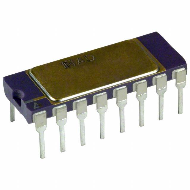
| 供应商器件封装 | 8-PDIP |
| 偏转电压—最大值 | 5 mV |
| 共模抑制比—最小值 | 65 dB |
| 关闭 | No Shutdown |
| 其它名称 | *LM392N/NOPB |
| 包装 | 管件 |
| 商标 | Texas Instruments |
| 增益带宽生成 | 1 MHz |
| 安装类型 | 通孔 |
| 安装风格 | Through Hole |
| 封装 | Tube |
| 封装/外壳 | 8-DIP(0.300",7.62mm) |
| 封装/箱体 | PDIP-8 |
| 工作电源电压 | 3 V to 32 V, +/- 1.5 V to +/- 16 V |
| 工厂包装数量 | 40 |
| 应用 | 传感器放大器 |
| 最大工作温度 | + 70 C |
| 最小双重电源电压 | +/- 1.5 V |
| 最小工作温度 | 0 C |
| 标准包装 | 40 |
| 比较器类型 | Precision |
| 电源电压-最大 | 32 V |
| 电源电压-最小 | 3 V |
| 电源电流 | 2 mA |
| 类型 | 放大器,比较器 |
| 系列 | LM392-N |
| 输入偏压电流—最大 | 400 nA |
| 输入电压范围—最大 | 32 V |
| 输入补偿电压 | 5 mV |
| 输出电流 | 16 mA |
| 输出类型 | CMOS/TTL |
| 通道数量 | 2 Channel |


PDF Datasheet 数据手册内容提取
LM392-N www.ti.com SNOSBT5D–APRIL1998–REVISEDMARCH2013 lm392-N Low Power Operational Amplifier/Voltage Comparator CheckforSamples:LM392-N FEATURES DESCRIPTION 1 • WidePowerSupplyVoltageRange The lm392-N series consists of 2 independent 2 building block circuits. One is a high gain, internally – SingleSupply:3Vto32V frequencycompensatedoperationalamplifier,andthe – DualSupply: ±1.5Vto ±16V other is a precision voltage comparator. Both the • LowSupplyCurrentDrain—Essentially operational amplifier and the voltage comparator IndependentofSupplyVoltage:600μA have been specifically designed to operate from a single power supply over a wide range of voltages. • LowInputBiasingCurrent:50nA Both circuits have input stages which will common- • LowInputOffsetVoltage:2mV mode input down to ground when operating from a • LowInputOffsetCurrent:5nA single power supply. Operation from split power supplies is also possible and the low power supply • InputCommon-ModeVoltageRangeIncludes current is independent of the magnitude of the supply Ground voltage. • DifferentialInputVoltageRangeEqualtothe Application areas include transducer amplifier with PowerSupplyVoltage pulseshaper,DCgainblockwithleveldetector,VCO, • ADDITIONALOPAMPFEATURES as well as all conventional operational amplifier or – InternallyFrequencyCompensatedfor voltage comparator circuits. Both circuits can be UnityGain operated directly from the standard 5 VDC power supply voltage used in digital systems, and the output – LargeDCVoltageGain: 100dB of the comparator will interface directly with either – WideBandwidth(UnityGain):1MHz TTL or CMOS logic. In addition, the low power drain – LargeOutputVoltageSwing:0VtoV+− makes the lm392-N extremely useful in the design of 1.5V portableequipment. • ADDITIONALCOMPARATORFEATURES – LowOutputSaturationVoltage:250mVat4 mA – OutputVoltageCompatiblewithallTypes ofLogicSystems ADVANTAGES • EliminatesNeedforDualPowerSupplies • AnInternallyCompensatedOpAmpanda PrecisionComparatorintheSamePackage • AllowsSensingatorNearGround • PowerDrainSuitableforBatteryOperation • Pin-OutistheSameasBoththeLM358Dual OpAmpandtheLM393DualComparator 1 Pleasebeawarethatanimportantnoticeconcerningavailability,standardwarranty,anduseincriticalapplicationsof TexasInstrumentssemiconductorproductsanddisclaimerstheretoappearsattheendofthisdatasheet. Alltrademarksarethepropertyoftheirrespectiveowners. 2 PRODUCTIONDATAinformationiscurrentasofpublicationdate. Copyright©1998–2013,TexasInstrumentsIncorporated Products conform to specifications per the terms of the Texas Instruments standard warranty. Production processing does not necessarilyincludetestingofallparameters.
LM392-N SNOSBT5D–APRIL1998–REVISEDMARCH2013 www.ti.com Connection Diagram TopView (AmplifierA=Comparator) (AmplifierB=OperationalAmplifier) Figure1. SOICandPDIPPackages SeePackageNumbersD0008AandP0008E Thesedeviceshavelimitedbuilt-inESDprotection.Theleadsshouldbeshortedtogetherorthedeviceplacedinconductivefoam duringstorageorhandlingtopreventelectrostaticdamagetotheMOSgates. 2 SubmitDocumentationFeedback Copyright©1998–2013,TexasInstrumentsIncorporated ProductFolderLinks:LM392-N
LM392-N www.ti.com SNOSBT5D–APRIL1998–REVISEDMARCH2013 Absolute Maximum Ratings (1)(2) lm392-N SupplyVoltage,V+ 32Vor±16V DifferentialInputVoltage 32V InputVoltage −0.3Vto+32V PowerDissipation (3) MoldedDIP(LM392N) 820mW SmallOutlinePackage(LM392M) 530mW OutputShort-CircuittoGround (4) Continuous InputCurrent(V <−0.3V ) (5) 50mA IN DC OperatingTemperatureRange 0°Cto+70°C StorageTemperatureRange −65°Cto+150°C LeadTemperature(Soldering,10seconds) 260°C ESDratingtobedetermined. SolderingInformation Dual-in-LinePackage Soldering(10seconds) 260°C SmallOutlinePackage VaporPhase(60seconds) 215°C Infrared(15seconds) 220°C (1) “AbsoluteMaximumRatings”indicatelimitsbeyondwhichdamagetothedevicemayoccur.OperatingRatingsindicateconditionsfor whichthedeviceisfunctional,butdonotensurespecificperformancelimits. (2) IfMilitary/Aerospacespecifieddevicesarerequired,pleasecontacttheTexasInstrumentsSalesOffice/Distributorsforavailabilityand specifications. (3) Foroperatingattemperaturesabove25°C,thelm392-Nmustbederatedbasedona125°Cmaximumjunctiontemperatureanda thermalresistanceof122°C/Wwhichappliesforthedevicesolderedinaprintedcircuitboard,operatinginstillairambient.The dissipationisthetotalofbothamplifiers—useexternalresistors,wherepossible,toallowtheamplifiertosaturateortoreducethepower whichisdissipatedintheintegratedcircuit. (4) ShortcircuitsfromtheoutputtoV+cancauseexcessiveheatingandeventualdestruction.Whenconsideringshortcircuitstoground, themaximumoutputcurrentisapproximately40mAfortheopampand30mAforthecomparatorindependentofthemagnitudeofV+. Atvaluesofsupplyvoltageinexcessof15V,continuousshortcircuitscanexceedthepowerdissipationratingsandcauseeventual destruction. (5) Thisinputcurrentwillonlyexistwhenthevoltageatanyoftheinputleadsisdrivennegative.Itisduetothecollector-basejunctionof theinputPNPtransistorsbecomingforwardbiasedandtherebyactingasinputdiodeclamps.Inadditiontothisdiodeaction,thereis alsolateralNPNparasitictransistoractionontheICchip.Thistransistoractioncancausetheoutputvoltagesoftheamplifierstogoto theV+voltagelevel(ortogroundforalargeoverdrive)forthetimedurationthataninputisdrivennegative.Thisisnotdestructiveand normaloutputstateswillre-establishwhentheinputvoltage,whichwasnegative,againreturnstoavaluegreaterthan−0.3V(at25°C). Electrical Characteristics (V+=5V ;specificationsapplytobothamplifiersunlessotherwisestated) (1) DC lm392-N Parameter Conditions Units Min Typ Max InputOffsetVoltage T =25°C, (2) ±2 ±5 mV A InputBiasCurrent IN(+)orIN(−),T =25°C, (3),V =0V 50 250 nA A CM InputOffsetCurrent IN(+)−IN(−),T =25°C ±5 ±50 nA A InputCommon-ModeVoltageRange V+=30V ,T =25°C, (4) 0 V+−1.5 V DC A SupplyCurrent R =∞,V+=30V 1 2 mA L SupplyCurrent R =∞,V+=5V 0.5 1 mA L (1) ThesespecificationsapplyforV+=5V,unlessotherwisestated.Forthelm392-N,temperaturespecificationsarelimitedto0°C≤T ≤ A +70°C. (2) Atoutputswitchpoint,V ≃1.4V,R =0ΩwithV+from5Vto30V;andoverthefullinputcommon-moderange(0VtoV+−1.5V). O S (3) ThedirectionoftheinputcurrentisoutoftheICduetothePNPinputstage.Thiscurrentisessentiallyconstant,independentofthe stateoftheoutputsonoloadingchangeexistsontheinputlines. (4) Theinputcommon-modevoltageoreitherinputsignalvoltageshouldnotbeallowedtogonegativebymorethan0.3V.Theupperend ofthecommon-modevoltagerangeisV+−1.5V,buteitherorbothinputscangoto32Vwithoutdamage. Copyright©1998–2013,TexasInstrumentsIncorporated SubmitDocumentationFeedback 3 ProductFolderLinks:LM392-N
LM392-N SNOSBT5D–APRIL1998–REVISEDMARCH2013 www.ti.com Electrical Characteristics (continued) (V+=5V ;specificationsapplytobothamplifiersunlessotherwisestated)(1) DC lm392-N Parameter Conditions Units Min Typ Max Amplifier-to-AmplifierCoupling f=1kHzto20kHz,T =25°C,InputReferred, (5) −100 dB A InputOffsetVoltage (2) ±7 mV InputBiasCurrent IN(+)orIN(−) 400 nA InputOffsetCurrent IN(+)−IN(−) 150 nA InputCommon-ModeVoltageRange V+=30V , (4) 0 V+−2 V DC DifferentialInputVoltage KeepAllV 's≥0V (orV−,ifused) (6) 32 V IN DC OPAMPONLY LargeSignalVoltageGain V+=15V ,V swing=1V to11V ,R =2 25 100 V/mV DC o DC DC L kΩ,T =25°C A OutputVoltageSwing R =2kΩ,T =25°C 0 V+−1.5 V L A Common-ModeRejectionRatio DC,T =25°C,V =0,V toV+−1.5V 65 70 dB A CM DC DC PowerSupplyRejectionRatio DC,T =25°C 65 100 dB A OutputCurrentSource V =1V ,V =0V , VI+N=(+)15V D,CV I=N(2−)V ,TDC=25°C 20 40 mA DC o DC A OutputCurrentSink V =1V ,V =0V , 10 20 mA IN(−) DC IN(+) DC V+=15V ,V =2V ,T =25°C DC o DC A V =1V ,V =0V , 12 50 µA IN(−) DC IN(+) DC V+=15V ,V =200mV,T =25°C DC o A InputOffsetVoltageDrift R =0Ω 7 μV/°C S InputOffsetCurrentDrift R =0Ω 10 pA /°C S DC COMPARATORONLY VoltageGain R ≥15kΩ,V+=15V ,T =25°C 50 200 V/mV L DC A LargeSignalResponseTime(7) V =TTLLogicSwing,V =1.4V 300 ns IN REF DC V =5V ,R =5.1kΩ,T =25°C RL DC L A ResponseTime V =5V ,R =5.1kΩ,T =25°C 1.3 µs RL DC L A OutputSinkCurrent V =1V ,V =0V , 6 16 mA IN(−) DC IN(+) DC V ≥1.5V ,T =25°C O DC A SaturationVoltage V ≥1V ,V =0, 250 400 mV IN(−) DC IN(+) I ≤4mA,T =25°C SINK A V ≥1V ,V =0, 700 mV IN(−) DC IN(+) I ≤4mA SINK OutputLeakageCurrent V =0,V ≥1V , 0.1 nA IN(−) IN(+) DC V =5V ,T =25°C o DC A V =0,V ≥1V , 1.0 μA IN(−) IN(+) DC V =30V o DC (5) Duetoproximityofexternalcomponents,insurethatcouplingisnotoriginatingviathestraycapacitancebetweentheseexternalparts. Thistypicallycanbedetectedasthistypeofcapacitivecouplingincreasesathigherfrequencies. (6) Positiveexcursionsofinputvoltagemayexceedthepowersupplylevel.Aslongastheotherinputvoltageremainswithinthecommon- moderange,thecomparatorwillprovideaproperoutputstate.Theinputvoltagetotheopampshouldnotexceedthepowersupply level.Theinputvoltagestatemustnotbelessthan−0.3V(or0.3Vbelowthemagnitudeofthenegativepowersupply,ifused)oneither amplifier. (7) Theresponsetimespecifiedisfora100mVinputstepwith5mVoverdrive.Forlargeroverdrivesignals300nscanbeobtained. 4 SubmitDocumentationFeedback Copyright©1998–2013,TexasInstrumentsIncorporated ProductFolderLinks:LM392-N
LM392-N www.ti.com SNOSBT5D–APRIL1998–REVISEDMARCH2013 Schematic Diagram Copyright©1998–2013,TexasInstrumentsIncorporated SubmitDocumentationFeedback 5 ProductFolderLinks:LM392-N
LM392-N SNOSBT5D–APRIL1998–REVISEDMARCH2013 www.ti.com APPLICATION HINTS PleaserefertotheapplicationhintssectionoftheLM193andtheLM158datasheets. 6 SubmitDocumentationFeedback Copyright©1998–2013,TexasInstrumentsIncorporated ProductFolderLinks:LM392-N
LM392-N www.ti.com SNOSBT5D–APRIL1998–REVISEDMARCH2013 REVISION HISTORY ChangesfromRevisionC(March2013)toRevisionD Page • ChangedlayoutofNationalDataSheettoTIformat............................................................................................................ 6 Copyright©1998–2013,TexasInstrumentsIncorporated SubmitDocumentationFeedback 7 ProductFolderLinks:LM392-N
PACKAGE OPTION ADDENDUM www.ti.com 19-Mar-2015 PACKAGING INFORMATION Orderable Device Status Package Type Package Pins Package Eco Plan Lead/Ball Finish MSL Peak Temp Op Temp (°C) Device Marking Samples (1) Drawing Qty (2) (6) (3) (4/5) LM392M NRND SOIC D 8 95 TBD Call TI Call TI 0 to 70 LM392 M LM392M/NOPB ACTIVE SOIC D 8 95 Green (RoHS CU SN Level-1-260C-UNLIM 0 to 70 LM392 & no Sb/Br) M LM392MX/NOPB ACTIVE SOIC D 8 2500 Green (RoHS CU SN Level-1-260C-UNLIM 0 to 70 LM392 & no Sb/Br) M LM392N/NOPB ACTIVE PDIP P 8 40 Green (RoHS CU SN Level-1-NA-UNLIM 0 to 70 LM & no Sb/Br) 392N (1) The marketing status values are defined as follows: ACTIVE: Product device recommended for new designs. LIFEBUY: TI has announced that the device will be discontinued, and a lifetime-buy period is in effect. NRND: Not recommended for new designs. Device is in production to support existing customers, but TI does not recommend using this part in a new design. PREVIEW: Device has been announced but is not in production. Samples may or may not be available. OBSOLETE: TI has discontinued the production of the device. (2) Eco Plan - The planned eco-friendly classification: Pb-Free (RoHS), Pb-Free (RoHS Exempt), or Green (RoHS & no Sb/Br) - please check http://www.ti.com/productcontent for the latest availability information and additional product content details. TBD: The Pb-Free/Green conversion plan has not been defined. Pb-Free (RoHS): TI's terms "Lead-Free" or "Pb-Free" mean semiconductor products that are compatible with the current RoHS requirements for all 6 substances, including the requirement that lead not exceed 0.1% by weight in homogeneous materials. Where designed to be soldered at high temperatures, TI Pb-Free products are suitable for use in specified lead-free processes. Pb-Free (RoHS Exempt): This component has a RoHS exemption for either 1) lead-based flip-chip solder bumps used between the die and package, or 2) lead-based die adhesive used between the die and leadframe. The component is otherwise considered Pb-Free (RoHS compatible) as defined above. Green (RoHS & no Sb/Br): TI defines "Green" to mean Pb-Free (RoHS compatible), and free of Bromine (Br) and Antimony (Sb) based flame retardants (Br or Sb do not exceed 0.1% by weight in homogeneous material) (3) MSL, Peak Temp. - The Moisture Sensitivity Level rating according to the JEDEC industry standard classifications, and peak solder temperature. (4) There may be additional marking, which relates to the logo, the lot trace code information, or the environmental category on the device. (5) Multiple Device Markings will be inside parentheses. Only one Device Marking contained in parentheses and separated by a "~" will appear on a device. If a line is indented then it is a continuation of the previous line and the two combined represent the entire Device Marking for that device. (6) Lead/Ball Finish - Orderable Devices may have multiple material finish options. Finish options are separated by a vertical ruled line. Lead/Ball Finish values may wrap to two lines if the finish value exceeds the maximum column width. Addendum-Page 1
PACKAGE OPTION ADDENDUM www.ti.com 19-Mar-2015 Important Information and Disclaimer:The information provided on this page represents TI's knowledge and belief as of the date that it is provided. TI bases its knowledge and belief on information provided by third parties, and makes no representation or warranty as to the accuracy of such information. Efforts are underway to better integrate information from third parties. TI has taken and continues to take reasonable steps to provide representative and accurate information but may not have conducted destructive testing or chemical analysis on incoming materials and chemicals. TI and TI suppliers consider certain information to be proprietary, and thus CAS numbers and other limited information may not be available for release. In no event shall TI's liability arising out of such information exceed the total purchase price of the TI part(s) at issue in this document sold by TI to Customer on an annual basis. Addendum-Page 2
PACKAGE MATERIALS INFORMATION www.ti.com 5-Feb-2016 TAPE AND REEL INFORMATION *Alldimensionsarenominal Device Package Package Pins SPQ Reel Reel A0 B0 K0 P1 W Pin1 Type Drawing Diameter Width (mm) (mm) (mm) (mm) (mm) Quadrant (mm) W1(mm) LM392MX/NOPB SOIC D 8 2500 330.0 12.4 6.5 5.4 2.0 8.0 12.0 Q1 PackMaterials-Page1
PACKAGE MATERIALS INFORMATION www.ti.com 5-Feb-2016 *Alldimensionsarenominal Device PackageType PackageDrawing Pins SPQ Length(mm) Width(mm) Height(mm) LM392MX/NOPB SOIC D 8 2500 367.0 367.0 35.0 PackMaterials-Page2
PACKAGE OUTLINE D0008A SOIC - 1.75 mm max height SCALE 2.800 SMALL OUTLINE INTEGRATED CIRCUIT C SEATING PLANE .228-.244 TYP [5.80-6.19] .004 [0.1] C A PIN 1 ID AREA 6X .050 [1.27] 8 1 2X .189-.197 [4.81-5.00] .150 NOTE 3 [3.81] 4X (0 -15 ) 4 5 8X .012-.020 B .150-.157 [0.31-0.51] .069 MAX [3.81-3.98] .010 [0.25] C A B [1.75] NOTE 4 .005-.010 TYP [0.13-0.25] 4X (0 -15 ) SEE DETAIL A .010 [0.25] .004-.010 0 - 8 [0.11-0.25] .016-.050 [0.41-1.27] DETAIL A (.041) TYPICAL [1.04] 4214825/C 02/2019 NOTES: 1. Linear dimensions are in inches [millimeters]. Dimensions in parenthesis are for reference only. Controlling dimensions are in inches. Dimensioning and tolerancing per ASME Y14.5M. 2. This drawing is subject to change without notice. 3. This dimension does not include mold flash, protrusions, or gate burrs. Mold flash, protrusions, or gate burrs shall not exceed .006 [0.15] per side. 4. This dimension does not include interlead flash. 5. Reference JEDEC registration MS-012, variation AA. www.ti.com
EXAMPLE BOARD LAYOUT D0008A SOIC - 1.75 mm max height SMALL OUTLINE INTEGRATED CIRCUIT 8X (.061 ) [1.55] SYMM SEE DETAILS 1 8 8X (.024) [0.6] SYMM (R.002 ) TYP [0.05] 5 4 6X (.050 ) [1.27] (.213) [5.4] LAND PATTERN EXAMPLE EXPOSED METAL SHOWN SCALE:8X SOLDER MASK SOLDER MASK METAL OPENING OPENING METAL UNDER SOLDER MASK EXPOSED METAL EXPOSED METAL .0028 MAX .0028 MIN [0.07] [0.07] ALL AROUND ALL AROUND NON SOLDER MASK SOLDER MASK DEFINED DEFINED SOLDER MASK DETAILS 4214825/C 02/2019 NOTES: (continued) 6. Publication IPC-7351 may have alternate designs. 7. Solder mask tolerances between and around signal pads can vary based on board fabrication site. www.ti.com
EXAMPLE STENCIL DESIGN D0008A SOIC - 1.75 mm max height SMALL OUTLINE INTEGRATED CIRCUIT 8X (.061 ) [1.55] SYMM 1 8 8X (.024) [0.6] SYMM (R.002 ) TYP [0.05] 5 4 6X (.050 ) [1.27] (.213) [5.4] SOLDER PASTE EXAMPLE BASED ON .005 INCH [0.125 MM] THICK STENCIL SCALE:8X 4214825/C 02/2019 NOTES: (continued) 8. Laser cutting apertures with trapezoidal walls and rounded corners may offer better paste release. IPC-7525 may have alternate design recommendations. 9. Board assembly site may have different recommendations for stencil design. www.ti.com
None
IMPORTANTNOTICEANDDISCLAIMER TIPROVIDESTECHNICALANDRELIABILITYDATA(INCLUDINGDATASHEETS),DESIGNRESOURCES(INCLUDINGREFERENCE DESIGNS),APPLICATIONOROTHERDESIGNADVICE,WEBTOOLS,SAFETYINFORMATION,ANDOTHERRESOURCES“ASIS” ANDWITHALLFAULTS,ANDDISCLAIMSALLWARRANTIES,EXPRESSANDIMPLIED,INCLUDINGWITHOUTLIMITATIONANY IMPLIEDWARRANTIESOFMERCHANTABILITY,FITNESSFORAPARTICULARPURPOSEORNON-INFRINGEMENTOFTHIRD PARTYINTELLECTUALPROPERTYRIGHTS. TheseresourcesareintendedforskilleddevelopersdesigningwithTIproducts.Youaresolelyresponsiblefor(1)selectingtheappropriate TIproductsforyourapplication,(2)designing,validatingandtestingyourapplication,and(3)ensuringyourapplicationmeetsapplicable standards,andanyothersafety,security,orotherrequirements.Theseresourcesaresubjecttochangewithoutnotice.TIgrantsyou permissiontousetheseresourcesonlyfordevelopmentofanapplicationthatusestheTIproductsdescribedintheresource.Other reproductionanddisplayoftheseresourcesisprohibited.NolicenseisgrantedtoanyotherTIintellectualpropertyrightortoanythird partyintellectualpropertyright.TIdisclaimsresponsibilityfor,andyouwillfullyindemnifyTIanditsrepresentativesagainst,anyclaims, damages,costs,losses,andliabilitiesarisingoutofyouruseoftheseresources. TI’sproductsareprovidedsubjecttoTI’sTermsofSale(www.ti.com/legal/termsofsale.html)orotherapplicabletermsavailableeitheron ti.comorprovidedinconjunctionwithsuchTIproducts.TI’sprovisionoftheseresourcesdoesnotexpandorotherwisealterTI’sapplicable warrantiesorwarrantydisclaimersforTIproducts. MailingAddress:TexasInstruments,PostOfficeBox655303,Dallas,Texas75265 Copyright©2019,TexasInstrumentsIncorporated