ICGOO在线商城 > 集成电路(IC) > PMIC - 电源控制器,监视器 > LM3880MFE-1AC/NOPB

 Datasheet下载
- 型号: LM3880MFE-1AC/NOPB
- 制造商: Texas Instruments
- 库位|库存: xxxx|xxxx
- 要求:
| 数量阶梯 | 香港交货 | 国内含税 |
| +xxxx | $xxxx | ¥xxxx |
查看当月历史价格
查看今年历史价格
LM3880MFE-1AC/NOPB产品简介:
ICGOO电子元器件商城为您提供LM3880MFE-1AC/NOPB由Texas Instruments设计生产,在icgoo商城现货销售,并且可以通过原厂、代理商等渠道进行代购。 LM3880MFE-1AC/NOPB价格参考¥1.45-¥1.45。Texas InstrumentsLM3880MFE-1AC/NOPB封装/规格:PMIC - 电源控制器,监视器, Power Supply Controller Power Supply Sequencer SOT-23-6。您可以下载LM3880MFE-1AC/NOPB参考资料、Datasheet数据手册功能说明书,资料中有LM3880MFE-1AC/NOPB 详细功能的应用电路图电压和使用方法及教程。
Texas Instruments的LM3880MFE-1AC/NOPB是一款电源管理集成电路(PMIC),属于电源控制器和监视器类别。它主要用于提供高效、可靠的电源监控和保护功能,广泛应用于各种需要稳定电源供应和电压监测的电子设备中。

 应用场景:

1. 消费电子产品:
   - 智能家居设备:如智能音箱、智能灯泡等,这些设备需要稳定的电源管理和低功耗设计,LM3880MFE-1AC/NOPB可以确保设备在不同工作模式下的电源稳定性。
   - 便携式设备:如平板电脑、智能手机等,该芯片可以帮助延长电池寿命,并确保设备在充电或使用过程中不会因电压波动而损坏。

2. 工业自动化:
   - 传感器模块:在工业环境中,传感器需要持续稳定的电源供应,以确保数据采集的准确性。LM3880MFE-1AC/NOPB可以为传感器提供可靠的电源管理和电压监控。
   - PLC(可编程逻辑控制器):用于工厂自动化控制的PLC系统中,该芯片可以防止因电源问题导致的系统故障,提高系统的可靠性和稳定性。

3. 通信设备:
   - 基站和路由器:这些设备通常需要24小时不间断运行,LM3880MFE-1AC/NOPB可以通过监控电源状态,确保设备在极端条件下仍能正常工作。
   - 无线模块:如Wi-Fi、蓝牙模块等,该芯片可以帮助优化电源管理,减少不必要的能耗。

4. 医疗设备:
   - 便携式医疗仪器:如血糖仪、心率监测仪等,这些设备对电源的稳定性要求极高,LM3880MFE-1AC/NOPB可以确保设备在使用过程中不会因电源问题影响测量结果。
   - 监护设备:如心电图机、呼吸机等,该芯片可以提供实时电源监控,确保设备在紧急情况下仍能正常运行。

5. 汽车电子:
   - 车载信息系统:如导航系统、娱乐系统等,LM3880MFE-1AC/NOPB可以确保这些系统在车辆启动、怠速等不同状态下都能获得稳定的电源供应。
   - 安全系统:如倒车雷达、摄像头等,该芯片可以防止因电源波动导致的安全隐患。

总之,LM3880MFE-1AC/NOPB凭借其高效、可靠的电源管理和监控功能,适用于多种应用场景,特别是在需要高稳定性和低功耗的场合中表现出色。
| 参数 | 数值 |
| 产品目录 | 集成电路 (IC)半导体 |
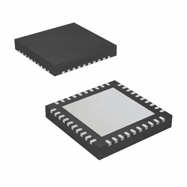
| 描述 | IC PWR SUPPLY SEQUENCER SOT23-6监控电路 Power Sequencer 6-SOT-23 -40 to 125 |
| 产品分类 | |
| 品牌 | Texas Instruments |
| 产品手册 | |
| 产品图片 |
|
| rohs | 符合RoHS无铅 / 符合限制有害物质指令(RoHS)规范要求 |
| 产品系列 | 电源管理 IC,监控电路,Texas Instruments LM3880MFE-1AC/NOPB- |
| NumberofInputsMonitored | 1 Input |
| 数据手册 | |
| 产品型号 | LM3880MFE-1AC/NOPB |
| 产品培训模块 | http://www.digikey.cn/PTM/IndividualPTM.page?site=cn&lang=zhs&ptm=30141 |
| 产品种类 | 监控电路 |
| 人工复位 | No Manual Reset |
| 供应商器件封装 | SOT-23-6 |
| 其它名称 | LM3880MFE-1AC |
| 制造商产品页 | http://www.ti.com/general/docs/suppproductinfo.tsp?distId=10&orderablePartNumber=LM3880MFE-1AC/NOPB |
| 包装 | 带卷 (TR) |
| 商标 | Texas Instruments |
| 安装类型 | 表面贴装 |
| 封装 | Reel |
| 封装/外壳 | SOT-23-6 |
| 封装/箱体 | SOT-23-6 |
| 工作温度 | -40°C ~ 125°C |
| 工作电源电流 | 25 uA |
| 工厂包装数量 | 250 |
| 应用 | 电源序列发生器 |
| 最小工作温度 | - 40 C |
| 标准包装 | 250 |
| 电压-电源 | 2.7 V ~ 5.5 V |
| 电压-输入 | - |
| 电池备用开关 | No Backup |
| 电流-电源 | 25µA |
| 电源电压-最大 | 5.5 V |
| 电源电压-最小 | 2.7 V |
| 监视器 | No Watchdog |
| 类型 | Voltage Sequencers |
| 系列 | LM3880 |
| 被监测输入数 | 3 Input |
| 设计资源 | http://www.digikey.com/product-highlights/cn/zh/texas-instruments-webench-design-center/3176 |
| 输出类型 | Open Collector / Drain |


- 商务部:美国ITC正式对集成电路等产品启动337调查
- 曝三星4nm工艺存在良率问题 高通将骁龙8 Gen1或转产台积电
- 太阳诱电将投资9.5亿元在常州建新厂生产MLCC 预计2023年完工
- 英特尔发布欧洲新工厂建设计划 深化IDM 2.0 战略
- 台积电先进制程称霸业界 有大客户加持明年业绩稳了
- 达到5530亿美元!SIA预计今年全球半导体销售额将创下新高
- 英特尔拟将自动驾驶子公司Mobileye上市 估值或超500亿美元
- 三星加码芯片和SET,合并消费电子和移动部门,撤换高东真等 CEO
- 三星电子宣布重大人事变动 还合并消费电子和移动部门
- 海关总署:前11个月进口集成电路产品价值2.52万亿元 增长14.8%


PDF Datasheet 数据手册内容提取
Product Order Technical Tools & Support & Folder Now Documents Software Community LM3880 SNVS451L–AUGUST2006–REVISEDNOVEMBER2018 LM3880 Three-Rail Simple Power Sequencer 1 Features 3 Description • QualifiedforAutomotiveApplications The LM3880 simple power supply sequencer offers 1 the easiest method to control power up sequencing • SimpleSolutionforSequencing3VoltageRails and power down sequencing of multiple Independent fromaSingleInputSignal voltage rails. By staggering the startup sequence, it is • EasilyCascadeupto3DevicestoSequenceas possible to avoid latch conditions or large in-rush Manyas9VoltageRails currentsthatcanaffectthereliabilityofthesystem. • Power-UpandPower-DownControl Available in a 6-pin SOT-23-6 package, the Simple • Tiny2.9-mmx1.9-mmFootprint Sequencer contains a precision enable pin and three open-drain output flags. The open-drain output flags • LowQuiescentCurrentof25µA permit that they can be pulled up to distinct voltage • InputVoltageRangeof2.7Vto5.5V supplies separate from the sequencer V (so long DD • StandardTimingOptionsAvailable as they do not exceed the recommended maximum voltage of 0.3V greater than V ), so as to interface DD 2 Applications with ICs requiring a range of different enable signals. When the LM3880 is enabled, the three output flags • AdvancedDriverAssistanceSystems(ADAS) will sequentially release, after individual time delays, • AutomotiveCameraModules thus permitting the connected power supplies to start • SecurityCameras up. The output flags will follow a reverse sequence duringpowerdowntoavoidlatchconditions. • Servers • NetworkingElements EPROM capability allows every delay and sequence to be fully adjustable. Contact Texas Instruments if a • FPGAPowerSupplySequencing nonstandardconfigurationisrequired. • MicroprocessorandMicrocontrollerSequencing • MultipleSupplySequencing DeviceInformation(1) PARTNUMBER PACKAGE BODYSIZE(NOM) LM3880 DBVSOT(6) 2.90mm×1.60mm (1) For all available packages, see the orderable addendum at theendofthedatasheet. SimplePowerSupplySequencing Input Supply 1 VCC Power Enable Supply 1 FLAG1 6 Power FLAG2 5 Enable Enable 3 EN Supply 2 FLAG3 4 Enable Power GND Supply 3 2 1 An IMPORTANT NOTICE at the end of this data sheet addresses availability, warranty, changes, use in safety-critical applications, intellectualpropertymattersandotherimportantdisclaimers.PRODUCTIONDATA.
LM3880 SNVS451L–AUGUST2006–REVISEDNOVEMBER2018 www.ti.com Table of Contents 1 Features.................................................................. 1 7.4 DeviceFunctionalModes........................................12 2 Applications........................................................... 1 8 ApplicationandImplementation........................ 13 3 Description............................................................. 1 8.1 ApplicationInformation............................................13 4 RevisionHistory..................................................... 2 8.2 TypicalApplication..................................................13 8.3 Do'sandDon'ts ......................................................15 5 PinConfigurationandFunctions......................... 3 9 PowerSupplyRecommendations...................... 17 6 Specifications......................................................... 4 10 Layout................................................................... 17 6.1 AbsoluteMaximumRatings......................................4 6.2 ESDRatings..............................................................4 10.1 LayoutGuidelines.................................................17 6.3 RecommendedOperatingConditions.......................4 10.2 LayoutExample....................................................17 6.4 ThermalInformation..................................................4 11 DeviceandDocumentationSupport................. 19 6.5 ElectricalCharacteristics...........................................5 11.1 DeviceSupport......................................................19 6.6 TypicalCharacteristics..............................................7 11.2 CommunityResources..........................................20 7 DetailedDescription.............................................. 9 11.3 Trademarks...........................................................20 7.1 Overview...................................................................9 11.4 ElectrostaticDischargeCaution............................20 7.2 FunctionalBlockDiagram.........................................9 11.5 Glossary................................................................20 7.3 FeatureDescription...................................................9 12 Mechanical,Packaging,andOrderable Information........................................................... 20 4 Revision History NOTE:Pagenumbersforpreviousrevisionsmaydifferfrompagenumbersinthecurrentversion. ChangesfromRevisionK(February2016)toRevisionL Page • UpdatedFeaturestospecifyhowmanyrailscanbesequencedbyasingledevice ............................................................ 1 • Addedfeaturethatdevicescanbecascaded ....................................................................................................................... 1 • SpecifieddevicedimensionsinFeatures............................................................................................................................... 1 • SpecifiedFPGAPowerSupplySequencinginApplications.................................................................................................. 1 • AddednoteindescriptionaboutopendrainFLAGpins......................................................................................................... 1 • AddedI/OcolumntoPinFunctionstable............................................................................................................................... 3 • ChangedPartNomenclaturesectiontoDeviceNomenclaturesection................................................................................ 19 ChangesfromRevisionJ(December2014)toRevisionK Page • ChangedHandlingRatingstoESDRatingsandmovedstoragetemperaturetoAbsoluteMaximumRatings.....................4 • Removed“CustomizedTimingandSequence”section ...................................................................................................... 12 • Addedcrossreferencestotimingdiagrams......................................................................................................................... 19 ChangesfromRevisionI(March2013)toRevisionJ Page • AddedHandlingRatingtable,FeatureDescriptionsection,DeviceFunctionalModes,Applicationand Implementationsection,PowerSupplyRecommendationssection,Layoutsection,DeviceandDocumentation Supportsection,andMechanical,Packaging,andOrderableInformationsection ............................................................... 4 ChangesfromRevisionH(March2013)toRevisionI Page • ChangedlayoutofNationalDataSheettoTIformat........................................................................................................... 19 2 SubmitDocumentationFeedback Copyright©2006–2018,TexasInstrumentsIncorporated ProductFolderLinks:LM3880
LM3880 www.ti.com SNVS451L–AUGUST2006–REVISEDNOVEMBER2018 5 Pin Configuration and Functions DBVPackage 6-PinSOT-23 TopView VCC 1 6 FLAG1 GND 2 5 FLAG2 EN 3 4 FLAG3 PinFunctions PIN I/O(1) DESCRIPTION NAME NO. EN 3 I Precisionenablepin FLAG1 6 O Open-drainoutput1 FLAG2 5 O Open-drainoutput2 FLAG3 4 O Open-drainoutput3 GND 2 G Ground VCC 1 I Inputsupply (1) I=input,O=output,G=ground Copyright©2006–2018,TexasInstrumentsIncorporated SubmitDocumentationFeedback 3 ProductFolderLinks:LM3880
LM3880 SNVS451L–AUGUST2006–REVISEDNOVEMBER2018 www.ti.com 6 Specifications 6.1 Absolute Maximum Ratings overoperatingfree-airtemperature(unlessotherwisenoted) (1)(2) MIN MAX UNIT VCC –0.3 6 V EN,FLAG1,FLAG2,FLAG3 –0.3 6 V MaximumFlagONcurrent 50 mA MaximumJunctiontemperature 150 °C Leadtemperature(Soldering,5s) 260 °C StoragetemperatureT –65 150 °C stg (1) StressesbeyondthoselistedunderAbsoluteMaximumRatingsmaycausepermanentdamagetothedevice.Thesearestressratings only,whichdonotimplyfunctionaloperationofthedeviceattheseoranyotherconditionsbeyondthoseindicatedunderRecommended OperatingConditions.Exposuretoabsolute-maximum-ratedconditionsforextendedperiodsmayaffectdevicereliability. (2) IfMilitary/Aerospacespecifieddevicesarerequired,pleasecontacttheTexasInstrumentsSalesOffice/Distributorsforavailabilityand specifications. 6.2 ESD Ratings VALUE UNIT V Electrostaticdischarge Humanbodymodel(HBM),perANSI/ESDA/JEDECJS-001,allpins (1) ±2 kV (ESD) (1) JEDECdocumentJEP155statesthat500-VHBMallowssafemanufacturingwithastandardESDcontrolprocess. 6.3 Recommended Operating Conditions overoperatingfree-airtemperaturerange(unlessotherwisenoted) MIN MAX UNIT VCCtoGND 2.7 5.5 V EN,FLAG1,FLAG2,FLAG3 –0.3 V +0.3 V CC Junctiontemperature –40 125 °C 6.4 Thermal Information LM3880 THERMALMETRIC(1) DBV(SOT-23) UNIT 6PINS R Junction-to-ambientthermalresistance 187.6 °C/W θJA R Junction-to-case(top)thermalresistance 127.4 °C/W θJC(top) R Junction-to-boardthermalresistance 31.5 °C/W θJB ψ Junction-to-topcharacterizationparameter 23.3 °C/W JT ψ Junction-to-boardcharacterizationparameter 31.0 °C/W JB (1) Formoreinformationabouttraditionalandnewthermalmetrics,seetheICPackageThermalMetricsapplicationreport,SPRA953. 4 SubmitDocumentationFeedback Copyright©2006–2018,TexasInstrumentsIncorporated ProductFolderLinks:LM3880
LM3880 www.ti.com SNVS451L–AUGUST2006–REVISEDNOVEMBER2018 6.5 Electrical Characteristics LimitsapplytoalltimingoptionsandV =3.3V,unlessotherwisespecified.MinimumandMaximumlimitsapplyoverthefull CC OperatingTemperatureRange(T =-40°Cto+125°C)andarespecifiedthroughtest,designorstatisticalcorrelation.Typical J valuesrepresentthemostlikelyparametricnormatT =25°Candareprovidedforreferencepurposesonly. J PARAMETER TESTCONDITIONS MIN(1) TYP(2) MAX(1) UNIT I OperatingQuiescentcurrent 25 80 µA Q OPEN-DRAINFLAGS I FLAGxLeakageCurrent V =3.3V 1 20 nA FLAG FLAGx V FLAGxOutputVoltageLow I =1.2mA 0.4 V OL FLAGx POWER-UPSEQUENCE t Timerdelay1accuracy AllOtherTimingOptions –15% 15% d1 2msTimingOption –20% 20% t Timerdelay2accuracy AllOtherTimingOptions –15% 15% d2 2msTimingOption –20% 20% t Timerdelay3accuracy AllOtherTimingOptions –15% 15% d3 2msTimingOption –20% 20% POWER-DOWNSEQUENCE t Timerdelay4accuracy AllOtherTimingOptions –15% 15% d4 2msTimingOption –20% 20% t Timerdelay5accuracy AllOtherTimingOptions –15% 15% d5 2msTimingOption –20% 20% t Timerdelay6accuracy AllOtherTimingOptions –15% 15% d6 2msTimingOption –20% 20% TIMINGDELAYERROR (t –400 Ratiooftimingdelays Forx=1or4 95% 105% d(x) µs)/t d(x+1) Forx=1or4,2msoption 90% 110% t /t Ratiooftimingdelays Forx=2or5 95% 105% d(x) d(x+1) Forx=2or5,2msoption 90% 110% ENABLEPIN V ENpinthreshold 1.0 1.25 1.4 V EN I ENpinpullupcurrent V =0V 7 µA EN EN (1) Limitsare100%productiontestedat25°.LimitsovertheoperatingtemperaturerangeareensuredthroughcorrelationusingStatistical QualityControl(SQC)methods.ThelimitsareusedtocalculateTI'sAverageOutgoingQualityLevel(AOQL). (2) Typicalnumbersareat25°Candrepresentthemostlikelyparametricnorm. TimingRequirements EN FLAG1 FLAG2 FLAG3 td1 td2 td3 AllstandardoptionsuseSequence1foroutputflagsriseandfallorder.Refertosection11.1.2fordetailsofdifferent sequencespossible. Figure1. Power-UpSequence Copyright©2006–2018,TexasInstrumentsIncorporated SubmitDocumentationFeedback 5 ProductFolderLinks:LM3880
LM3880 SNVS451L–AUGUST2006–REVISEDNOVEMBER2018 www.ti.com EN FLAG1 FLAG2 FLAG3 td4 td5 td6 AllstandardoptionsuseSequence1foroutputflagsriseandfallorder.Refertosection11.1.2fordetailsofdifferent sequencespossible. Figure2. Power-DownSequence 6 SubmitDocumentationFeedback Copyright©2006–2018,TexasInstrumentsIncorporated ProductFolderLinks:LM3880
LM3880 www.ti.com SNVS451L–AUGUST2006–REVISEDNOVEMBER2018 6.6 Typical Characteristics 30 26 29 25 28 27 24 26 )A )A ( PQ 25 ( PQ 23 I 24 I 23 22 22 21 21 20 20 2.5 3 3.5 4 4.5 5 5.5 -40-25-10 5 20 35 50 65 80 95110125 TEMPERATURE (oC) VCC (V) Figure3.QuiescentCurrentvsVCC Figure4.QuiescentCurrentvsTemperature(VCC=3.3V) 1.232 1.230 1.228 1.226 RISING )V 1.224 ( N FALLING VE 1.222 1.220 1.218 1.216 1.214 -40-25-10 5 20 35 50 65 80 95 110125 TEMPERATURE (°C) Figure5.EnableThresholdvsTemperature Figure6.TimeDelay(30ms)vsVcc Figure7.TimeDelayRatiovsTemperature Figure8.TimeDelay(30ms)vsTemperature Copyright©2006–2018,TexasInstrumentsIncorporated SubmitDocumentationFeedback 7 ProductFolderLinks:LM3880
LM3880 SNVS451L–AUGUST2006–REVISEDNOVEMBER2018 www.ti.com Typical Characteristics (continued) Figure9.FlagV vsVcc(R =100kΩ) Figure10.FlagVoltagevsCurrent OL FLAG 8 SubmitDocumentationFeedback Copyright©2006–2018,TexasInstrumentsIncorporated ProductFolderLinks:LM3880
LM3880 www.ti.com SNVS451L–AUGUST2006–REVISEDNOVEMBER2018 7 Detailed Description 7.1 Overview The LM3880 simple power supply sequencer provides a simple solution for sequencing multiple rails in a controlled manner. Six independent timers are integrated to control the timing sequence (power up and power down)ofthreeopen-drainoutputflags.Theseflagspermitconnectiontoeitherashutdownorenablepinoflinear regulators and switchers to control the operation of the power supplies. This allows design of a complete power systemwithoutconcernforlargeinrushcurrentsorlatch-upconditionsthatcanoccur. The timing sequence of the device is controlled entirely by the enable (EN) pin. Upon power up, all the flags are held low until this precision enable is pulled high. When the EN pin is asserted, the power-up sequence starts. An internal counter delays the first flag (FLAG1) from rising until a fixed time period has expired. When the first flag is released, another timer will begin to delay the release of the second flag (FLAG2). This process repeats untilallthreeflagshavesequentiallybeenreleased. The power-down sequence is the same as power-up sequence, but in reverse. When the EN pin is deasserted a timer will begin that delays the third flag (FLAG3) from pulling low. The second and first flag will then follow in a sequential manner after their appropriate delays. The three timers that are used to control the power-down schemecanalsobeindividuallyprogrammedandarecompletelyindependentofthepower-uptimers. 7.2 Functional Block Diagram VCC FLAG1 7 µA tD1 tD2 EN + tD3 FLAG2 Timing Sequence Delay 1.25 V Generation tD4 Control Master tD5 Clock FLAG3 tD6 EEPROM (Factory Set) GND 7.3 Feature Description 7.3.1 EnablePinOperation The timing sequence of the LM3880 is controlled by the assertion of the enable signal. The enable pin is designedwithaninternalcomparator,referencedtoabandgapvoltage(1.25V),toprovideaprecisionthreshold. This allows a delayed timing to be externally set using a capacitor or to start the sequencing based on a certain event, such as a line voltage reaching 90% of nominal. For an additional delayed sequence from the rail poweringVCC,simplyattachacapacitortotheENpinasshowninFigure11. Copyright©2006–2018,TexasInstrumentsIncorporated SubmitDocumentationFeedback 9 ProductFolderLinks:LM3880
LM3880 SNVS451L–AUGUST2006–REVISEDNOVEMBER2018 www.ti.com Feature Description (continued) 7 µA EN + Enable CEN 1.25 V Figure11. CapacitorTiming Using the internal pullup current source to charge the external capacitor (C ) the enable pin delay can be EN calculatedbyEquation1: 1.25V x CEN tenable_delay = 7 PA (1) A resistor divider can also be used to enable the device based on a certain voltage threshold. Take care when sizingtheresistordividertoincludetheeffectsoftheinternalcurrentsource. One of the features of the EN pin is that it provides glitch free operation. The first timer will start counting at a rising threshold, but will always reset if the EN pin is deasserted before the first output flag is released. This can beshowninFigure12: EN FLAG1 td1 Figure12. ENGlitch 7.3.2 IncompleteSequenceOperation If the enable signal remains high for the entire power-up sequence, then the part will operate as shown in the standard timing diagrams. However, if the enable signal is de-asserted before the power-up sequence is completed the part will enter a controlled shutdown. This allows the system to walk through a controlled power cycling, preventing any latch conditions from occurring. This state only occurs if the enable pin is deasserted afterthecompletionoftimer1,butbeforetheentirepower-upsequenceiscompleted. When this event occurs, the falling edge of EN pin resets the current timer and will allow the remaining power-up cycle to complete before beginning the power-down sequence. The power down sequence starts approximately 120 ms after the final power-up flag. This allows output voltages in the system to stabilize before everything is shutdown.AnexampleofthisoperationcanbeseeninFigure13: 10 SubmitDocumentationFeedback Copyright©2006–2018,TexasInstrumentsIncorporated ProductFolderLinks:LM3880
LM3880 www.ti.com SNVS451L–AUGUST2006–REVISEDNOVEMBER2018 Feature Description (continued) EN FLAG1 FLAG2 FLAG3 td1 td2 td3 120 ms td4 td5 td6 Figure13. IncompletePower-UpSequence When the enable signal is deasserted, the part will commence its power-down sequence. If the enable signal is pulled high before the power-down sequence is completed, the part will ensure completion of the power-down sequence before starting power-up. This ensures that the system does not partially power down and power up and helps prevent latch-up events, such as in FPGAs and microprocessors. This state only occurs if the enable pinispulledhighafterthecompletionoftimer1,butbeforetheentirepower-downsequenceiscompleted. Whenthiseventoccurs,therisingedgeofenablepinresetsthecurrenttimerandwillallowtheremainingpower- down cycle to complete before beginning the power-up sequence. The power-up sequence starts approximately 120 ms after the final power-down flag. This allows the system to fully shut down before it is powered up. An exampleofthisoperationcanbeseeninFigure14: EN FLAG1 FLAG2 FLAG3 ttd1t ttd2t ttd3t t120 mst ttd4t ttd5t ttd6t Figure14. IncompletePower-DownSequence All the internal timers are generated by a master clock that has an extremely low tempco. This allows for tight accuracy across temperature and a consistent ratio between the individual timers. There is a slight additional delay of approximately 400 µs to timers 1 and 4, which is a result of the EPROM refresh. This refresh time is in additiontotheprogrammeddelaytimeandwillbealmostinsignificanttoallbuttheshortestoftimerdelays. Copyright©2006–2018,TexasInstrumentsIncorporated SubmitDocumentationFeedback 11 ProductFolderLinks:LM3880
LM3880 SNVS451L–AUGUST2006–REVISEDNOVEMBER2018 www.ti.com 7.4 Device Functional Modes 7.4.1 PowerUpWithENPin The timing sequence of the Simple Power Supply Sequencer is controlled entirely by the enable (EN) pin. Upon power up, all the flags are held low until this precision enable is pulled high. After the EN pin is asserted, the power-upsequencewillcommence. 7.4.2 PowerDownWithENPin When EN pin is deasserted, the power down sequence will commence. A timer will begin that delays the third flag (FLAG3) from pulling low. The second and first flag will then follow in a sequential manner after their appropriatedelays. 12 SubmitDocumentationFeedback Copyright©2006–2018,TexasInstrumentsIncorporated ProductFolderLinks:LM3880
LM3880 www.ti.com SNVS451L–AUGUST2006–REVISEDNOVEMBER2018 8 Application and Implementation NOTE Information in the following applications sections is not part of the TI component specification, and TI does not warrant its accuracy or completeness. TI’s customers are responsible for determining suitability of components for their purposes. Customers should validateandtesttheirdesignimplementationtoconfirmsystemfunctionality. 8.1 Application Information 8.1.1 OpenDrainFlagsPullup The Simple Power Supply Sequencer contains three open-drain output flags which need to be pulled up for properoperation.100-kΩ resistorscanbeusedaspullupresistors. 8.1.2 EnabletheDevice SeeEnablePinOperation. 8.2 Typical Application 8.2.1 SimpleSequencingofThreePowerSupplies The Simple Power Supply Sequencer is used to implement a power-up and power-down sequence of three powersupplies. Sequence 1 for the LM3880, e.g. orderable part number LM3880MF-1AA has a power-up sequence (1 – 2 – 3) and power-down sequence (3 – 2 –1). See Table 3 and Table 4 for other sequence options or contact TI if other sequenceoptionsaredesired. Figure15. TypicalApplicationCircuit Copyright©2006–2018,TexasInstrumentsIncorporated SubmitDocumentationFeedback 13 ProductFolderLinks:LM3880
LM3880 SNVS451L–AUGUST2006–REVISEDNOVEMBER2018 www.ti.com Typical Application (continued) 8.2.1.1 DesignRequirements For this design example, use the parameters listed in Table 1 as the input parameters. The circuit shown in Figure15canhavevariouspower-downsequencesdependingonthesequencethepartisprogrammedfor.See Table3fordifferentpower-downsequenceoptions. Table1.DesignParameters DESIGNPARAMETER EXAMPLEVALUE InputSupplyvoltagerange 2.7Vto5.5V FlagOutputvoltage,ENhigh InputSupply FlagOutputvoltage,ENlow 0V FlagTimingDelay 30ms Power-UpSequence 1-2-3 Power-DownSequence 3-2-1 8.2.1.2 DetailedDesignProcedure Table2.BillofMaterials DESIGNATOR DESCRIPTION DEVICE QUANTITY MANUFACTURER U1 LM3880,Sequence1,30mstiming LM3880 1 TexasInstruments R1 100-kΩResistor,0603 CRCW0603100KFKEA 1 Vishay R2 100-kΩResistor,0603 CRCW0603100KFKEA 1 Vishay R3 100-kΩResistor,0603 CRCW0603100KFKEA 1 Vishay This application uses the Sequence 1 and 30-ms timing options of the Simple Power Supply Sequencer. See ApplicationCurvesfordetailsonthesequenceandtimingoption. 8.2.1.3 ApplicationCurves Figure16.Power-UpSequencefor Figure17.Power-DownSequencefor LM3880MF-1AE LM3880MF-1AE 14 SubmitDocumentationFeedback Copyright©2006–2018,TexasInstrumentsIncorporated ProductFolderLinks:LM3880
LM3880 www.ti.com SNVS451L–AUGUST2006–REVISEDNOVEMBER2018 8.2.2 SequencingUsingIndependentFlagSupply For applications requiring a flag output voltage that is different from the VCC, a separate Flag Supply may be used to pullup the open-drain outputs of the simple power supply sequencer. This is useful when interfacing the flag outputs with inputs that require a different voltage than VCC. The designer must ensure the flag supply voltageisnottakenaboveVCC+0.3VasspecifiedintheRecommendedOperatingConditions. Figure18. SequencingUsingIndependentFlagSupply 8.3 Do's and Don'ts Connecting the EN pin to VCC is not recommended. During power up, the EN voltage should be kept below the EN threshold until VCC rises above the minimum operating voltage. This will be violated if EN is connected to VCC, and undefined operation at the flag outputs can occur, especially during slow VCC rising slew rates. For systems requiring only power-up sequencing, a capacitor at the EN pin can be used to create a delay or a resistor divider can be used to enable the device based on a certain voltage threshold. While these solutions will work for power-up, it will not power-down the flag outputs in sequential fashion since the flag outputs will simply follow the input supply. For systems requiring both power-up and power-down sequencing, an external enable signal should be used, such as a GPIO signal from a microcontroller, to properly control power-up and power- downoftheflagoutputs. Copyright©2006–2018,TexasInstrumentsIncorporated SubmitDocumentationFeedback 15 ProductFolderLinks:LM3880
LM3880 SNVS451L–AUGUST2006–REVISEDNOVEMBER2018 www.ti.com Do's and Don'ts (continued) Figure19. RecommendedENConnection 16 SubmitDocumentationFeedback Copyright©2006–2018,TexasInstrumentsIncorporated ProductFolderLinks:LM3880
LM3880 www.ti.com SNVS451L–AUGUST2006–REVISEDNOVEMBER2018 9 Power Supply Recommendations The VCC pin should be located as close as possible to the input supply (2.7–5.5 V). An input capacitor is not required but is recommended when noise might be present on the VCC pin. A 0.1-μF ceramic capacitor may be usedtobypassthisnoise. 10 Layout 10.1 Layout Guidelines • Pullup resistors should be connected between the flag output pins and a positive input supply, usually VCC. An independent flag supply may also be used. These resistors should be placed as close as possible to the Simple Power Supply Sequencer and the flag supply. Minimal trace length is recommended to make the connections.Atypicalvalueforthepullupresistorsis100kΩ. • For very tight sequencing requirements, minimal and equal trace lengths should be used to connect the flag outputs to the desired inputs. This will reduce any propagation delay and timing errors between the flag outputsalongtheline. 10.2 Layout Example Figure20andFigure21arelayoutexamplesfortheLM3880.TheseexamplesaretakenfromtheLM3880EVAL. Figure20. LM3880Top Copyright©2006–2018,TexasInstrumentsIncorporated SubmitDocumentationFeedback 17 ProductFolderLinks:LM3880
LM3880 SNVS451L–AUGUST2006–REVISEDNOVEMBER2018 www.ti.com Layout Example (continued) Figure21. LM3880Bottom 18 SubmitDocumentationFeedback Copyright©2006–2018,TexasInstrumentsIncorporated ProductFolderLinks:LM3880
LM3880 www.ti.com SNVS451L–AUGUST2006–REVISEDNOVEMBER2018 11 Device and Documentation Support 11.1 Device Support 11.1.1 Third-PartyProductsDisclaimer TI'S PUBLICATION OF INFORMATION REGARDING THIRD-PARTY PRODUCTS OR SERVICES DOES NOT CONSTITUTE AN ENDORSEMENT REGARDING THE SUITABILITY OF SUCH PRODUCTS OR SERVICES OR A WARRANTY, REPRESENTATION OR ENDORSEMENT OF SUCH PRODUCTS OR SERVICES, EITHER ALONEORINCOMBINATIONWITHANYTIPRODUCTORSERVICE. 11.1.2 DeviceNomenclature ThelistofpartsavailabletoorderappearinthePackageOptionAddendum. Figure22. DeviceNomenclature Table3.SequenceDesignatorTable (1) FLAGORDER SEQUENCENUMBER POWERUP POWERDOWN 1 1-2-3 3-2-1 2 1-2-3 3-1-2 3 1-2-3 2-3-1 4 1-2-3 2-1-3 5 1-2-3 1-3-2 6 1-2-3 1-2-3 (1) SeeFigure1andFigure2. Table4.TimingDesignatorTable(1) TIMING DELAYS(ms) DESIGNATOR t t t t t t d1 d2 d3 d4 d5 d6 AA 10 10 10 10 10 10 AB 30 30 30 30 30 30 AC 60 60 60 60 60 60 AD 120 120 120 120 120 120 AE 2 2 2 2 2 2 AF 16 16 16 16 16 16 (1) SeeFigure1andFigure2. Copyright©2006–2018,TexasInstrumentsIncorporated SubmitDocumentationFeedback 19 ProductFolderLinks:LM3880
LM3880 SNVS451L–AUGUST2006–REVISEDNOVEMBER2018 www.ti.com 11.2 Community Resources The following links connect to TI community resources. Linked contents are provided "AS IS" by the respective contributors. They do not constitute TI specifications and do not necessarily reflect TI's views; see TI's Terms of Use. TIE2E™OnlineCommunity TI'sEngineer-to-Engineer(E2E)Community.Createdtofostercollaboration amongengineers.Ate2e.ti.com,youcanaskquestions,shareknowledge,exploreideasandhelp solveproblemswithfellowengineers. DesignSupport TI'sDesignSupport QuicklyfindhelpfulE2Eforumsalongwithdesignsupporttoolsand contactinformationfortechnicalsupport. 11.3 Trademarks E2EisatrademarkofTexasInstruments. 11.4 Electrostatic Discharge Caution Thesedeviceshavelimitedbuilt-inESDprotection.Theleadsshouldbeshortedtogetherorthedeviceplacedinconductivefoam duringstorageorhandlingtopreventelectrostaticdamagetotheMOSgates. 11.5 Glossary SLYZ022—TIGlossary. Thisglossarylistsandexplainsterms,acronyms,anddefinitions. 12 Mechanical, Packaging, and Orderable Information The following pages include mechanical, packaging, and orderable information. This information is the most current data available for the designated devices. This data is subject to change without notice and revision of thisdocument.Forbrowser-basedversionsofthisdatasheet,refertotheleft-handnavigation. 20 SubmitDocumentationFeedback Copyright©2006–2018,TexasInstrumentsIncorporated ProductFolderLinks:LM3880
PACKAGE OPTION ADDENDUM www.ti.com 6-Feb-2020 PACKAGING INFORMATION Orderable Device Status Package Type Package Pins Package Eco Plan Lead/Ball Finish MSL Peak Temp Op Temp (°C) Device Marking Samples (1) Drawing Qty (2) (6) (3) (4/5) LM3880MF-1AA NRND SOT-23 DBV 6 1000 TBD Call TI Call TI -40 to 125 F20A LM3880MF-1AA/NOPB ACTIVE SOT-23 DBV 6 1000 Green (RoHS SN Level-1-260C-UNLIM -40 to 125 F20A & no Sb/Br) LM3880MF-1AB/NOPB ACTIVE SOT-23 DBV 6 1000 Green (RoHS SN Level-1-260C-UNLIM -40 to 125 F21A & no Sb/Br) LM3880MF-1AC/NOPB ACTIVE SOT-23 DBV 6 1000 Green (RoHS SN Level-1-260C-UNLIM -40 to 125 F22A & no Sb/Br) LM3880MF-1AD/NOPB ACTIVE SOT-23 DBV 6 1000 Green (RoHS SN Level-1-260C-UNLIM -40 to 125 F23A & no Sb/Br) LM3880MF-1AE/NOPB ACTIVE SOT-23 DBV 6 1000 Green (RoHS SN Level-1-260C-UNLIM -40 to 125 F25A & no Sb/Br) LM3880MF-1AF/NOPB ACTIVE SOT-23 DBV 6 1000 Green (RoHS SN Level-1-260C-UNLIM -40 to 125 F31A & no Sb/Br) LM3880MFE-1AA/NOPB ACTIVE SOT-23 DBV 6 250 Green (RoHS SN Level-1-260C-UNLIM -40 to 125 F20A & no Sb/Br) LM3880MFE-1AB/NOPB ACTIVE SOT-23 DBV 6 250 Green (RoHS SN Level-1-260C-UNLIM -40 to 125 F21A & no Sb/Br) LM3880MFE-1AC/NOPB ACTIVE SOT-23 DBV 6 250 Green (RoHS SN Level-1-260C-UNLIM -40 to 125 F22A & no Sb/Br) LM3880MFE-1AD/NOPB ACTIVE SOT-23 DBV 6 250 Green (RoHS SN Level-1-260C-UNLIM -40 to 125 F23A & no Sb/Br) LM3880MFE-1AE/NOPB ACTIVE SOT-23 DBV 6 250 Green (RoHS SN Level-1-260C-UNLIM -40 to 125 F25A & no Sb/Br) LM3880MFE-1AF/NOPB ACTIVE SOT-23 DBV 6 250 Green (RoHS SN Level-1-260C-UNLIM -40 to 125 F31A & no Sb/Br) LM3880MFX-1AA/NOPB ACTIVE SOT-23 DBV 6 3000 Green (RoHS SN Level-1-260C-UNLIM -40 to 125 F20A & no Sb/Br) LM3880MFX-1AB/NOPB ACTIVE SOT-23 DBV 6 3000 Green (RoHS SN Level-1-260C-UNLIM -40 to 125 F21A & no Sb/Br) LM3880MFX-1AC/NOPB ACTIVE SOT-23 DBV 6 3000 Green (RoHS SN Level-1-260C-UNLIM -40 to 125 F22A & no Sb/Br) LM3880MFX-1AD/NOPB ACTIVE SOT-23 DBV 6 3000 Green (RoHS SN Level-1-260C-UNLIM -40 to 125 F23A & no Sb/Br) Addendum-Page 1
PACKAGE OPTION ADDENDUM www.ti.com 6-Feb-2020 Orderable Device Status Package Type Package Pins Package Eco Plan Lead/Ball Finish MSL Peak Temp Op Temp (°C) Device Marking Samples (1) Drawing Qty (2) (6) (3) (4/5) LM3880MFX-1AE/NOPB ACTIVE SOT-23 DBV 6 3000 Green (RoHS SN Level-1-260C-UNLIM -40 to 125 F25A & no Sb/Br) LM3880MFX-1AF/NOPB ACTIVE SOT-23 DBV 6 3000 Green (RoHS SN Level-1-260C-UNLIM -40 to 125 F31A & no Sb/Br) (1) The marketing status values are defined as follows: ACTIVE: Product device recommended for new designs. LIFEBUY: TI has announced that the device will be discontinued, and a lifetime-buy period is in effect. NRND: Not recommended for new designs. Device is in production to support existing customers, but TI does not recommend using this part in a new design. PREVIEW: Device has been announced but is not in production. Samples may or may not be available. OBSOLETE: TI has discontinued the production of the device. (2) RoHS: TI defines "RoHS" to mean semiconductor products that are compliant with the current EU RoHS requirements for all 10 RoHS substances, including the requirement that RoHS substance do not exceed 0.1% by weight in homogeneous materials. Where designed to be soldered at high temperatures, "RoHS" products are suitable for use in specified lead-free processes. TI may reference these types of products as "Pb-Free". RoHS Exempt: TI defines "RoHS Exempt" to mean products that contain lead but are compliant with EU RoHS pursuant to a specific EU RoHS exemption. Green: TI defines "Green" to mean the content of Chlorine (Cl) and Bromine (Br) based flame retardants meet JS709B low halogen requirements of <=1000ppm threshold. Antimony trioxide based flame retardants must also meet the <=1000ppm threshold requirement. (3) MSL, Peak Temp. - The Moisture Sensitivity Level rating according to the JEDEC industry standard classifications, and peak solder temperature. (4) There may be additional marking, which relates to the logo, the lot trace code information, or the environmental category on the device. (5) Multiple Device Markings will be inside parentheses. Only one Device Marking contained in parentheses and separated by a "~" will appear on a device. If a line is indented then it is a continuation of the previous line and the two combined represent the entire Device Marking for that device. (6) Lead/Ball Finish - Orderable Devices may have multiple material finish options. Finish options are separated by a vertical ruled line. Lead/Ball Finish values may wrap to two lines if the finish value exceeds the maximum column width. Important Information and Disclaimer:The information provided on this page represents TI's knowledge and belief as of the date that it is provided. TI bases its knowledge and belief on information provided by third parties, and makes no representation or warranty as to the accuracy of such information. Efforts are underway to better integrate information from third parties. TI has taken and continues to take reasonable steps to provide representative and accurate information but may not have conducted destructive testing or chemical analysis on incoming materials and chemicals. TI and TI suppliers consider certain information to be proprietary, and thus CAS numbers and other limited information may not be available for release. In no event shall TI's liability arising out of such information exceed the total purchase price of the TI part(s) at issue in this document sold by TI to Customer on an annual basis. OTHER QUALIFIED VERSIONS OF LM3880 : Addendum-Page 2
PACKAGE OPTION ADDENDUM www.ti.com 6-Feb-2020 •Automotive: LM3880-Q1 NOTE: Qualified Version Definitions: •Automotive - Q100 devices qualified for high-reliability automotive applications targeting zero defects Addendum-Page 3
PACKAGE MATERIALS INFORMATION www.ti.com 29-Sep-2019 TAPE AND REEL INFORMATION *Alldimensionsarenominal Device Package Package Pins SPQ Reel Reel A0 B0 K0 P1 W Pin1 Type Drawing Diameter Width (mm) (mm) (mm) (mm) (mm) Quadrant (mm) W1(mm) LM3880MF-1AA SOT-23 DBV 6 1000 178.0 8.4 3.2 3.2 1.4 4.0 8.0 Q3 LM3880MF-1AA/NOPB SOT-23 DBV 6 1000 178.0 8.4 3.2 3.2 1.4 4.0 8.0 Q3 LM3880MF-1AB/NOPB SOT-23 DBV 6 1000 178.0 8.4 3.2 3.2 1.4 4.0 8.0 Q3 LM3880MF-1AC/NOPB SOT-23 DBV 6 1000 178.0 8.4 3.2 3.2 1.4 4.0 8.0 Q3 LM3880MF-1AD/NOPB SOT-23 DBV 6 1000 178.0 8.4 3.2 3.2 1.4 4.0 8.0 Q3 LM3880MF-1AE/NOPB SOT-23 DBV 6 1000 178.0 8.4 3.2 3.2 1.4 4.0 8.0 Q3 LM3880MF-1AF/NOPB SOT-23 DBV 6 1000 178.0 8.4 3.2 3.2 1.4 4.0 8.0 Q3 LM3880MFE-1AA/NOPB SOT-23 DBV 6 250 178.0 8.4 3.2 3.2 1.4 4.0 8.0 Q3 LM3880MFE-1AB/NOPB SOT-23 DBV 6 250 178.0 8.4 3.2 3.2 1.4 4.0 8.0 Q3 LM3880MFE-1AC/NOPB SOT-23 DBV 6 250 178.0 8.4 3.2 3.2 1.4 4.0 8.0 Q3 LM3880MFE-1AD/NOPB SOT-23 DBV 6 250 178.0 8.4 3.2 3.2 1.4 4.0 8.0 Q3 LM3880MFE-1AE/NOPB SOT-23 DBV 6 250 178.0 8.4 3.2 3.2 1.4 4.0 8.0 Q3 LM3880MFE-1AF/NOPB SOT-23 DBV 6 250 178.0 8.4 3.2 3.2 1.4 4.0 8.0 Q3 LM3880MFX-1AA/NOPB SOT-23 DBV 6 3000 178.0 8.4 3.2 3.2 1.4 4.0 8.0 Q3 LM3880MFX-1AB/NOPB SOT-23 DBV 6 3000 178.0 8.4 3.2 3.2 1.4 4.0 8.0 Q3 LM3880MFX-1AC/NOPB SOT-23 DBV 6 3000 178.0 8.4 3.2 3.2 1.4 4.0 8.0 Q3 LM3880MFX-1AD/NOPB SOT-23 DBV 6 3000 178.0 8.4 3.2 3.2 1.4 4.0 8.0 Q3 LM3880MFX-1AE/NOPB SOT-23 DBV 6 3000 178.0 8.4 3.2 3.2 1.4 4.0 8.0 Q3 PackMaterials-Page1
PACKAGE MATERIALS INFORMATION www.ti.com 29-Sep-2019 Device Package Package Pins SPQ Reel Reel A0 B0 K0 P1 W Pin1 Type Drawing Diameter Width (mm) (mm) (mm) (mm) (mm) Quadrant (mm) W1(mm) LM3880MFX-1AF/NOPB SOT-23 DBV 6 3000 178.0 8.4 3.2 3.2 1.4 4.0 8.0 Q3 *Alldimensionsarenominal Device PackageType PackageDrawing Pins SPQ Length(mm) Width(mm) Height(mm) LM3880MF-1AA SOT-23 DBV 6 1000 210.0 185.0 35.0 LM3880MF-1AA/NOPB SOT-23 DBV 6 1000 210.0 185.0 35.0 LM3880MF-1AB/NOPB SOT-23 DBV 6 1000 210.0 185.0 35.0 LM3880MF-1AC/NOPB SOT-23 DBV 6 1000 210.0 185.0 35.0 LM3880MF-1AD/NOPB SOT-23 DBV 6 1000 210.0 185.0 35.0 LM3880MF-1AE/NOPB SOT-23 DBV 6 1000 210.0 185.0 35.0 LM3880MF-1AF/NOPB SOT-23 DBV 6 1000 210.0 185.0 35.0 LM3880MFE-1AA/NOPB SOT-23 DBV 6 250 210.0 185.0 35.0 LM3880MFE-1AB/NOPB SOT-23 DBV 6 250 210.0 185.0 35.0 LM3880MFE-1AC/NOPB SOT-23 DBV 6 250 210.0 185.0 35.0 LM3880MFE-1AD/NOPB SOT-23 DBV 6 250 210.0 185.0 35.0 LM3880MFE-1AE/NOPB SOT-23 DBV 6 250 210.0 185.0 35.0 LM3880MFE-1AF/NOPB SOT-23 DBV 6 250 210.0 185.0 35.0 LM3880MFX-1AA/NOPB SOT-23 DBV 6 3000 210.0 185.0 35.0 LM3880MFX-1AB/NOPB SOT-23 DBV 6 3000 210.0 185.0 35.0 LM3880MFX-1AC/NOPB SOT-23 DBV 6 3000 210.0 185.0 35.0 PackMaterials-Page2
PACKAGE MATERIALS INFORMATION www.ti.com 29-Sep-2019 Device PackageType PackageDrawing Pins SPQ Length(mm) Width(mm) Height(mm) LM3880MFX-1AD/NOPB SOT-23 DBV 6 3000 210.0 185.0 35.0 LM3880MFX-1AE/NOPB SOT-23 DBV 6 3000 210.0 185.0 35.0 LM3880MFX-1AF/NOPB SOT-23 DBV 6 3000 210.0 185.0 35.0 PackMaterials-Page3
PACKAGE OUTLINE DBV0006A SOT-23 - 1.45 mm max height SCALE 4.000 SMALL OUTLINE TRANSISTOR C 3.0 2.6 0.1 C 1.75 1.45 B A 1.45 MAX PIN 1 INDEX AREA 1 6 2X 0.95 3.05 2.75 1.9 5 2 4 3 0.50 6X 0.25 0.15 0.2 C A B (1.1) TYP 0.00 0.25 GAGE PLANE 0.22 TYP 0.08 8 TYP 0.6 0 0.3 TYP SEATING PLANE 4214840/B 03/2018 NOTES: 1. All linear dimensions are in millimeters. Any dimensions in parenthesis are for reference only. Dimensioning and tolerancing per ASME Y14.5M. 2. This drawing is subject to change without notice. 3. Body dimensions do not include mold flash or protrusion. Mold flash and protrusion shall not exceed 0.15 per side. 4. Leads 1,2,3 may be wider than leads 4,5,6 for package orientation. 5. Refernce JEDEC MO-178. www.ti.com
EXAMPLE BOARD LAYOUT DBV0006A SOT-23 - 1.45 mm max height SMALL OUTLINE TRANSISTOR PKG 6X (1.1) 1 6X (0.6) 6 SYMM 2 5 2X (0.95) 3 4 (R0.05) TYP (2.6) LAND PATTERN EXAMPLE EXPOSED METAL SHOWN SCALE:15X SOLDER MASK SOLDER MASK METAL UNDER METAL OPENING OPENING SOLDER MASK EXPOSED METAL EXPOSED METAL 0.07 MAX 0.07 MIN ARROUND ARROUND NON SOLDER MASK SOLDER MASK DEFINED DEFINED (PREFERRED) SOLDER MASK DETAILS 4214840/B 03/2018 NOTES: (continued) 6. Publication IPC-7351 may have alternate designs. 7. Solder mask tolerances between and around signal pads can vary based on board fabrication site. www.ti.com
EXAMPLE STENCIL DESIGN DBV0006A SOT-23 - 1.45 mm max height SMALL OUTLINE TRANSISTOR PKG 6X (1.1) 1 6X (0.6) 6 SYMM 2 5 2X(0.95) 3 4 (R0.05) TYP (2.6) SOLDER PASTE EXAMPLE BASED ON 0.125 mm THICK STENCIL SCALE:15X 4214840/B 03/2018 NOTES: (continued) 8. Laser cutting apertures with trapezoidal walls and rounded corners may offer better paste release. IPC-7525 may have alternate design recommendations. 9. Board assembly site may have different recommendations for stencil design. www.ti.com
IMPORTANTNOTICEANDDISCLAIMER TI PROVIDES TECHNICAL AND RELIABILITY DATA (INCLUDING DATASHEETS), DESIGN RESOURCES (INCLUDING REFERENCE DESIGNS), APPLICATION OR OTHER DESIGN ADVICE, WEB TOOLS, SAFETY INFORMATION, AND OTHER RESOURCES “AS IS” AND WITH ALL FAULTS, AND DISCLAIMS ALL WARRANTIES, EXPRESS AND IMPLIED, INCLUDING WITHOUT LIMITATION ANY IMPLIED WARRANTIES OF MERCHANTABILITY, FITNESS FOR A PARTICULAR PURPOSE OR NON-INFRINGEMENT OF THIRD PARTY INTELLECTUAL PROPERTY RIGHTS. These resources are intended for skilled developers designing with TI products. You are solely responsible for (1) selecting the appropriate TI products for your application, (2) designing, validating and testing your application, and (3) ensuring your application meets applicable standards, and any other safety, security, or other requirements. These resources are subject to change without notice. TI grants you permission to use these resources only for development of an application that uses the TI products described in the resource. Other reproduction and display of these resources is prohibited. No license is granted to any other TI intellectual property right or to any third party intellectual property right. TI disclaims responsibility for, and you will fully indemnify TI and its representatives against, any claims, damages, costs, losses, and liabilities arising out of your use of these resources. TI’s products are provided subject to TI’s Terms of Sale (www.ti.com/legal/termsofsale.html) or other applicable terms available either on ti.com or provided in conjunction with such TI products. TI’s provision of these resources does not expand or otherwise alter TI’s applicable warranties or warranty disclaimers for TI products. Mailing Address: Texas Instruments, Post Office Box 655303, Dallas, Texas 75265 Copyright © 2020, Texas Instruments Incorporated