ICGOO在线商城 > LM3677LEE-1.82/NOPB

 Datasheet下载
- 型号: LM3677LEE-1.82/NOPB
- 制造商: Texas Instruments
- 库位|库存: xxxx|xxxx
- 要求:
| 数量阶梯 | 香港交货 | 国内含税 |
| +xxxx | $xxxx | ¥xxxx |
查看当月历史价格
查看今年历史价格
LM3677LEE-1.82/NOPB产品简介:
ICGOO电子元器件商城为您提供LM3677LEE-1.82/NOPB由Texas Instruments设计生产,在icgoo商城现货销售,并且可以通过原厂、代理商等渠道进行代购。 提供LM3677LEE-1.82/NOPB价格参考以及Texas InstrumentsLM3677LEE-1.82/NOPB封装/规格参数等产品信息。 你可以下载LM3677LEE-1.82/NOPB参考资料、Datasheet数据手册功能说明书, 资料中有LM3677LEE-1.82/NOPB详细功能的应用电路图电压和使用方法及教程。
| 参数 | 数值 |
| 产品目录 | 集成电路 (IC)半导体 |
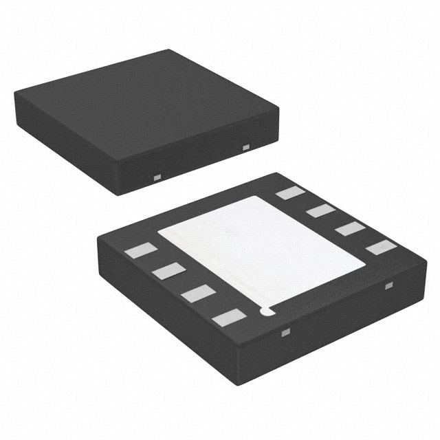
| 描述 | IC REG BCK SYNC 1.82V 0.6A 6-LLP稳压器—开关式稳压器 3MHz, 600mA Miniature Step-Down DC-DC Converter for Ultra Low Voltage Circuits 6-USON |
| 产品分类 | |
| 品牌 | Texas Instruments |
| 产品手册 | |
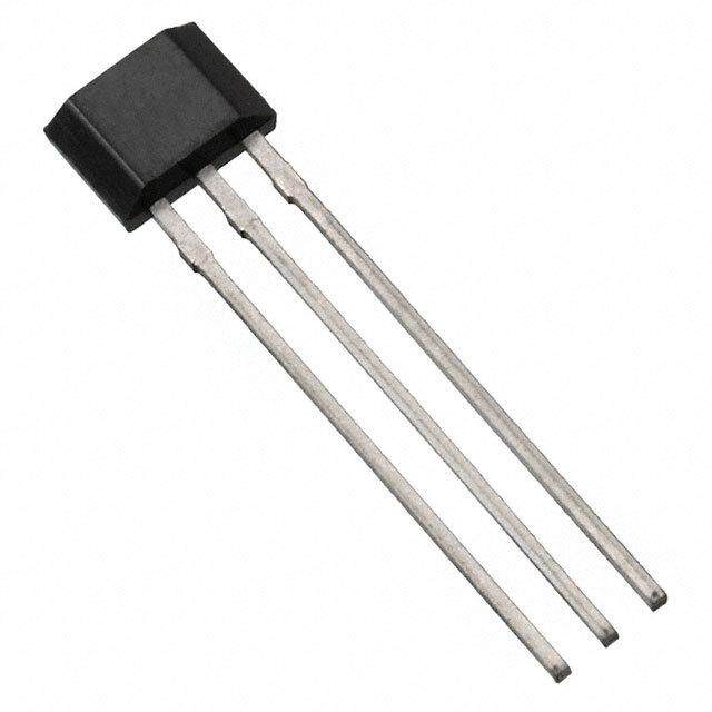
| 产品图片 |
|
| rohs | 符合RoHS无铅 / 符合限制有害物质指令(RoHS)规范要求 |
| 产品系列 | 电源管理 IC,稳压器—开关式稳压器,Texas Instruments LM3677LEE-1.82/NOPB- |
| 数据手册 | |
| 产品型号 | LM3677LEE-1.82/NOPB |
| PWM类型 | 电流/电压模式 |
| 产品目录页面 | |
| 产品种类 | 稳压器—开关式稳压器 |
| 供应商器件封装 | 6-LLP(2.0x1.5) |
| 关闭 | Shutdown |
| 其它名称 | LM3677LEE-1.82/NOPBDKR |
| 包装 | Digi-Reel® |
| 同步整流器 | 是 |
| 商标 | Texas Instruments |
| 安装类型 | 表面贴装 |
| 安装风格 | SMD/SMT |
| 封装 | Reel |
| 封装/外壳 | 6-UFDFN |
| 封装/箱体 | LLP EP |
| 工作温度 | -30°C ~ 85°C |
| 工厂包装数量 | 250 |
| 开关频率 | 3000 kHz |
| 拓扑结构 | Buck |
| 最大工作温度 | + 85 C |
| 最大输入电压 | 5.5 V |
| 最小工作温度 | - 30 C |
| 最小输入电压 | 2.7 V |
| 标准包装 | 1 |
| 电压-输入 | 2.7 V ~ 5.5 V |
| 电压-输出 | 1.82V |
| 电流-输出 | 600mA |
| 电源电压-最小 | 2.7 V |
| 电源电流 | 5 mA |
| 类型 | Step Down |
| 系列 | LM3677 |
| 输入电压 | 5.5 V |
| 输出数 | 1 |
| 输出电压 | 1.82 V |
| 输出电流 | 600 mA |
| 输出端数量 | 1 Output |
| 输出类型 | 固定 |
| 配用 | /product-detail/zh/LM3677LE-1.8EV/LM3677LE-1.8EV-ND/1882583/product-detail/zh/LM3677TL-1.8EV/LM3677TL-1.8EV-ND/1640688 |
| 频率-开关 | 3MHz |


- 商务部:美国ITC正式对集成电路等产品启动337调查
- 曝三星4nm工艺存在良率问题 高通将骁龙8 Gen1或转产台积电
- 太阳诱电将投资9.5亿元在常州建新厂生产MLCC 预计2023年完工
- 英特尔发布欧洲新工厂建设计划 深化IDM 2.0 战略
- 台积电先进制程称霸业界 有大客户加持明年业绩稳了
- 达到5530亿美元!SIA预计今年全球半导体销售额将创下新高
- 英特尔拟将自动驾驶子公司Mobileye上市 估值或超500亿美元
- 三星加码芯片和SET,合并消费电子和移动部门,撤换高东真等 CEO
- 三星电子宣布重大人事变动 还合并消费电子和移动部门
- 海关总署:前11个月进口集成电路产品价值2.52万亿元 增长14.8%


PDF Datasheet 数据手册内容提取
LM3677 www.ti.com SNVS502F–MARCH2007–REVISEDMAY2013 3MHz, 600mA Miniature Step-Down DC-DC Converter for Ultra Low Voltage Circuits CheckforSamples:LM3677 FEATURES APPLICATIONS 1 • 16µAtypicalquiescentcurrent • MobilePhones 2 • 600mAmaximumloadcapability • PDAs • 3MHzPWMfixedswitchingfrequency(typ.) • MP3Players • AutomaticPFM/PWMmodeswitching • W-LAN • Availablein5-bumpDSBGApackageand6-pin • PortableInstruments USONpackage • DigitalStillCameras • Internalsynchronousrectificationforhigh • PortableHardDiskDrives efficiency • Internalsoftstart DESCRIPTION • 0.01µAtypicalshutdowncurrent The LM3677 step-down DC-DC converter is optimized for powering ultra-low voltage circuits from • OperatesfromasingleLi-Ioncellbattery a single Li-Ion cell battery and input voltage rails from • Onlythreetinysurface-mountexternal 2.7V to 5.5V. It provides up to 600 mA load current componentsrequired(solutionsizelessthan over the entire input voltage range. The LM3677 is 20mm2) configured to different fixed voltage output options as • Currentoverloadandthermalshutdown well as an adjustable output voltage version range from1.2Vto3.3V. protection TYPICAL APPLICATION CIRCUITS VIN L1: 1.0 PH 2.7V to 5.5V VIN SW VOUT 1 5 CIN LM3677 COUT 4.7 PF GND 10 PF 2 EN FB 3 4 Figure1. TypicalApplicationCircuit VIN L1: 1.0 PH 2.7V to 5.5V VIN SW VOUT 1 5 CIN LM3677- COUT 4.7 PF GND ADJ C1 R1 10 PF 2 C2 R2 EN FB 3 4 Figure3. Efficiencyvs.OutputCurrent Figure2. TypicalApplicationCircuit-ADJ. (V =1.8V) Version OUT 1 Pleasebeawarethatanimportantnoticeconcerningavailability,standardwarranty,anduseincriticalapplicationsof TexasInstrumentssemiconductorproductsanddisclaimerstheretoappearsattheendofthisdatasheet. Alltrademarksarethepropertyoftheirrespectiveowners. 2 PRODUCTIONDATAinformationiscurrentasofpublicationdate. Copyright©2007–2013,TexasInstrumentsIncorporated Products conform to specifications per the terms of the Texas Instruments standard warranty. Production processing does not necessarilyincludetestingofallparameters.
LM3677 SNVS502F–MARCH2007–REVISEDMAY2013 www.ti.com DESCRIPTION (CONTINUED) The device offers superior features and performance for mobile phones and similar portable applications with complex power management systems. Automatic intelligent switching between PWM low-noise and PFM low- current mode offers improved system control. During PWM mode operation, the device operates at a fixed frequency of 3 MHz (typ). PWM mode drives loads from ~ 80 mA to 600 mA max. Hysteretic PFM mode extends the battery life by reducing the quiescent current to 16 µA (typ.) during light load and standby operation. Internal synchronous rectification provides high efficiency. In shutdown mode (Enable pin pulled down), the device turns offandreducesbatteryconsumptionto0.01µA(typ.). The LM3677 is available in a lead-free (NOPB) 5-bump DSBGA package and 6-pin USON package. A switching frequency of 3 MHz (typ.) allows use of tiny surface-mount components. Only three external surface-mount components,aninductorandtwoceramiccapacitors,arerequired. CONNECTION DIAGRAMS Vin A1 A3 GND GND A3 A1 Vin B2 SW SW B2 EN C1 C3 FB FB C3 C1 EN Top View Bottom View 5-BumpDSBGAPackage SeePackageNumberYZR0005 VIN 1 6 GND 6 GND VIN 1 SW 2 5 SW 5 SW SW 2 EN 3 4 FB 4 FB EN 3 TOP VIEW BOTTOM VIEW 6-PinUSONPackage SeePackageNumberNGE0006A PINDESCRIPTIONS(1) Name PinNo. Description V A1 1 Powersupplyinput.Connecttotheinputfiltercapacitor(Figure1). IN GND A3 6 Groundpin. EN C1 3 Enablepin.Thedeviceisinshutdownmodewhenvoltagetothispinis<0.4Vand enabledwhen>1.0V.Donotleavethispinfloating. FB C3 4 Feedbackanaloginput.Connectdirectlytotheoutputfiltercapacitor(FIGURE1). SW B2 2,5 SwitchingnodeconnectiontotheinternalPFETswitchandNFETsynchronous rectifier. (1) Foroutputvoltage1.2Vorlower,inputvoltageneedstobederatedtotherangeof2.7Vto5.0Vinordertoperformwithinspecification. Thesedeviceshavelimitedbuilt-inESDprotection.Theleadsshouldbeshortedtogetherorthedeviceplacedinconductivefoam duringstorageorhandlingtopreventelectrostaticdamagetotheMOSgates. 2 SubmitDocumentationFeedback Copyright©2007–2013,TexasInstrumentsIncorporated ProductFolderLinks:LM3677
LM3677 www.ti.com SNVS502F–MARCH2007–REVISEDMAY2013 ABSOLUTE MAXIMUM RATINGS(1)(2) IfMilitary/Aerospacespecifieddevicesarerequired,pleasecontacttheTexasInstrumentsSalesOffice/Distributorfor availabilityandspecifications. V Pin:VoltagetoGND −0.2Vto6.0V IN FB,SW,ENPin: (GND−0.2V)to (V +0.2V) IN ContinuousPowerDissipation (3) InternallyLimited JunctionTemperature(T ) +125°C J-MAX StorageTemperatureRange −65°Cto+150°C MaximumLeadTemperature 260°C (Soldering,10sec.) ESDRating (4) HumanBodyModel:AllPins 2.0kV MachineModel:AllPins 200V (1) AbsoluteMaximumRatingsindicatelimitsbeyondwhichdamagetothecomponentmayoccur.OperatingRatingsareconditionsunder whichoperationofthedeviceisspecified.OperatingRatingsdonotimplyperformancelimits.Forperformancelimitsandassociatedtest conditions,seetheElectricalCharacteristicstables. (2) IfMilitary/Aerospacespecifieddevicesarerequired,pleasecontacttheTexasInstrumentsSalesOffice/Distributorsfor availabilityandspecifications. (3) Internalthermalshutdowncircuitryprotectsthedevicefrompermanentdamage.ThermalshutdownengagesatT=150°C(typ.)and J disengagesatT=130°C(typ.). J (4) TheHumanbodymodelisa100pFcapacitordischargedthrougha1.5kΩresistorintoeachpin.Themachinemodelisa200pF capacitordischargeddirectlyintoeachpin.MIL-STD-8833015.7 OPERATING RATINGS(1), (2) InputVoltageRange 2.7Vto5.5V RecommendedLoadCurrent 0mAto600mA JunctionTemperature(T)Range −30°Cto+125°C J AmbientTemperature(T )Range (3) −30°Cto+85°C A (1) AbsoluteMaximumRatingsindicatelimitsbeyondwhichdamagetothecomponentmayoccur.OperatingRatingsareconditionsunder whichoperationofthedeviceisspecified.OperatingRatingsdonotimplyperformancelimits.Forperformancelimitsandassociatedtest conditions,seetheElectricalCharacteristicstables. (2) AllvoltagesarewithrespecttothepotentialattheGNDpin. (3) InApplicationswherehighpowerdissipationand/orpoorpackageresistanceispresent,themaximumambienttemperaturemayhave tobederated.Maximumambienttemperature(T )isdependentonthemaximumoperatingjunctiontemperature(T ),the A-MAX J-MAX maximumpowerdissipationofthedeviceintheapplication(P )andthejunctiontoambientthermalresistanceofthepackage(θ ) D-MAX JA intheapplication,asgivenbythefollowingequation:T =T −(θ xP ).RefertoDissipationratingtableforP values A-MAX J-MAX JA D-MAX D-MAX atdifferentambienttemperatures. THERMAL PROPERTIES Junction-to-AmbientThermalResistance(θ ) (1) 85°C/W JA (1) Junctiontoambientthermalresistanceishighlyapplicationandboardlayoutdependent.Inapplicationswherehighpowerdissipation exists,specialcaremustbegiventothermaldissipationissuesinboarddesign.Valuespecifiedhere85°C/Wisbasedon measurementresultsusinga4layerboardasperJEDECstandards. Copyright©2007–2013,TexasInstrumentsIncorporated SubmitDocumentationFeedback 3 ProductFolderLinks:LM3677
LM3677 SNVS502F–MARCH2007–REVISEDMAY2013 www.ti.com ELECTRICAL CHARACTERISTICS(1)(2)(3) LimitsinstandardtypefaceareforT =T =25°C.Limitsinboldfacetypeapplyovertheoperatingambienttemperature J A range(−30°C≤T ≤+85°C).Unlessotherwisenoted,specificationsapplytotheLM3677withV =EN=3.6V. A IN Parameter TestConditions Min Typ Max Units V InputVoltage (4) 2.7 5.5 V IN FeedbackVoltage(TL) -2.5 +2.5 V PWMmode % FB FeedbackVoltage(LE) -4.0 +4.0 V InternalReferenceVoltage 0.5 V REF I ShutdownSupplyCurrent EN=0V 0.01 1 µA SHDN I DCBiasCurrentintoV Noload,deviceisnotswitching 16 35 µA Q IN R Pin-PinResistanceforPFET V =V =3.6V,I =100mA 350 450 mΩ DSON(P) IN GS SW R Pin-PinResistanceforNFET V =V =3.6V,I =-100mA 150 250 mΩ DSON(N) IN GS SW I SwitchPeakCurrentLimit OpenLoop(5) 1085 1220 1375 mA LIM V LogicHighInput 1.0 V IH V LogicLowInput 0.4 V IL I Enable(EN)InputCurrent 0.01 1 µA EN F InternalOscillatorFrequency PWMMode 2.5 3 3.5 MHz OSC (1) AllvoltagesarewithrespecttothepotentialattheGNDpin. (2) MinandMaxlimitsarespecifiedbydesign,testorstatisticalanalysis.Typicalnumbersrepresentthemostlikelynorm. (3) TheparametersintheelectricalcharacteristictablearetestedunderopenloopconditionsatV =3.6Vunlessotherwisespecified.For IN performanceovertheinputvoltagerangeandclosedloopcondition,refertothedatasheetcurves. (4) Foroutputvoltage1.2Vorlower,inputvoltageneedstobederatedtotherangeof2.7Vto5.0Vinordertoperformwithinspecification. (5) Refertodatasheetcurvesforclosedloopdataanditsvariationwithregardstosupplyvoltageandtemperature.ElectricalCharacteristic tablereflectsopenloopdata(FB=0VandcurrentdrawnfromSWpinrampedupuntilcyclebycyclecurrentlimitisactivated).Closed loopcurrentlimitisthepeakinductorcurrentmeasuredintheapplicationcircuitbyincreasingoutputcurrentuntiloutputvoltagedrops by10%. DISSIPATION RATING TABLE T ≤25°C T =60°C T =85°C θ A A A JA PowerRating PowerRating PowerRating 85°C/W(4-layerboard) 1178mW 785mW 470mW DSBGA 117°C/W(4-layerboard) 855mW 556mW 342mW USON 4 SubmitDocumentationFeedback Copyright©2007–2013,TexasInstrumentsIncorporated ProductFolderLinks:LM3677
LM3677 www.ti.com SNVS502F–MARCH2007–REVISEDMAY2013 BLOCK DIAGRAM EN VIN SW Current Limit Comparator Undervoltage Ramp Soft + Lockout Generator Start - Ref1 PFM Current Comparator Thermal Bandgap 3 MHz + Shutdown Oscillator - Ref2 PWM Comparator Error + Amp - Control Logic Driver pfm_low VREF + pfm_hi 0.5V - Vcomp + 1.0V - + - Zero Crossing Comparator Frequency Compensation Fixed Ver FB GND Figure4. SimplifiedFunctionalDiagram Copyright©2007–2013,TexasInstrumentsIncorporated SubmitDocumentationFeedback 5 ProductFolderLinks:LM3677
LM3677 SNVS502F–MARCH2007–REVISEDMAY2013 www.ti.com TYPICAL PERFORMANCE CHARACTERISTICS LM3677,CircuitofFigure1,V =3.6V,V =1.8V,T =25°C,unlessotherwisenoted. IN OUT A QuiescentSupplyCurrentvs.SupplyVoltage (Switching) ShutdownCurrentvs.Temp Figure5. Figure6. SwitchingFrequencyvs.Temperature R vs.Temperature DS(ON) Figure7. Figure8. Open/ClosedLoopCurrentLimit OutputVoltagevs.SupplyVoltage vs.Temperature (V =1.8V) OUT Figure9. Figure10. 6 SubmitDocumentationFeedback Copyright©2007–2013,TexasInstrumentsIncorporated ProductFolderLinks:LM3677
LM3677 www.ti.com SNVS502F–MARCH2007–REVISEDMAY2013 TYPICAL PERFORMANCE CHARACTERISTICS (continued) LM3677,CircuitofFigure1,V =3.6V,V =1.8V,T =25°C,unlessotherwisenoted. IN OUT A OutputVoltagevs.SupplyVoltage OutputVoltagevs.Temperature (V =2.5V) (V =1.3V) OUT OUT Figure11. Figure12. OutputVoltagevs.Temperature OutputVoltagevs.Temperature (V =1.8V) (V =2.5V) OUT OUT Figure13. Figure14. OutputVoltagevs.OutputCurrent OutputVoltagevs.OutputCurrent (V =1.8V) (V =2.5V) OUT OUT Figure15. Figure16. Copyright©2007–2013,TexasInstrumentsIncorporated SubmitDocumentationFeedback 7 ProductFolderLinks:LM3677
LM3677 SNVS502F–MARCH2007–REVISEDMAY2013 www.ti.com TYPICAL PERFORMANCE CHARACTERISTICS (continued) LM3677,CircuitofFigure1,V =3.6V,V =1.8V,T =25°C,unlessotherwisenoted. IN OUT A Efficiencyvs.OutputCurrent Efficiencyvs.OutputCurrent (V =1.3V) (V =1.8V) OUT OUT Figure17. Figure18. Efficiencyvs.OutputCurrent OutputCurrentvs.InputVoltageatModeChangePoint (V =2.5V) (V =1.3V) OUT OUT Figure19. Figure20. OutputCurrentvs.InputVoltageatModeChangePoint OutputCurrentvs.InputVoltageatModeChangePoint (V =1.8V) (V =2.5V) OUT OUT Figure21. Figure22. 8 SubmitDocumentationFeedback Copyright©2007–2013,TexasInstrumentsIncorporated ProductFolderLinks:LM3677
LM3677 www.ti.com SNVS502F–MARCH2007–REVISEDMAY2013 TYPICAL PERFORMANCE CHARACTERISTICS (continued) LM3677,CircuitofFigure1,V =3.6V,V =1.8V,T =25°C,unlessotherwisenoted. IN OUT A LineTransientResponse LineTransientResponse V =1.3V(PWMMode) V =1.8V(PWMMode) OUT OUT Figure23. Figure24. LineTransientResponse LineTransientResponse V =1.8V(PWMMode) V =2.5V(PWMMode) OUT OUT Figure25. Figure26. LoadTransientResponse(V =1.3V) LoadTransientResponse(V =1.3V) OUT OUT (PFMMode1mAto50mA) (PFMMode50mAto1mA) Figure27. Figure28. Copyright©2007–2013,TexasInstrumentsIncorporated SubmitDocumentationFeedback 9 ProductFolderLinks:LM3677
LM3677 SNVS502F–MARCH2007–REVISEDMAY2013 www.ti.com TYPICAL PERFORMANCE CHARACTERISTICS (continued) LM3677,CircuitofFigure1,V =3.6V,V =1.8V,T =25°C,unlessotherwisenoted. IN OUT A LoadTransientResponse(V =1.8V) LoadTransientResponse(V =1.8V) OUT OUT (PFMMode1mAto50mA) (PFMMode50mAto1mA) Figure29. Figure30. LoadTransientResponse(V =2.5V) LoadTransientResponse(V =2.5V) OUT OUT (PFMMode1mAto50mA) (PFMMode50mAto1mA) Figure31. Figure32. ModeChangebyLoadTransients ModeChangebyLoadTransients V =1.3V(PFMtoPWM) V =1.3V(PWMtoPFM) OUT OUT Figure33. Figure34. 10 SubmitDocumentationFeedback Copyright©2007–2013,TexasInstrumentsIncorporated ProductFolderLinks:LM3677
LM3677 www.ti.com SNVS502F–MARCH2007–REVISEDMAY2013 TYPICAL PERFORMANCE CHARACTERISTICS (continued) LM3677,CircuitofFigure1,V =3.6V,V =1.8V,T =25°C,unlessotherwisenoted. IN OUT A ModeChangebyLoadTransients ModeChangebyLoadTransients V =1.8V(PFMtoPWM) V =1.8V(PWMtoPFM) OUT OUT Figure35. Figure36. LoadTransientResponse LoadTransientResponse V =1.3V(PWMMode) V =1.8V(PWMMode) OUT OUT Figure37. Figure38. LoadTransientResponse StartUpintoPWMMode V =2.5V(PWMMode) V =1.3V(OutputCurrent=300mA) OUT OUT Figure39. Figure40. Copyright©2007–2013,TexasInstrumentsIncorporated SubmitDocumentationFeedback 11 ProductFolderLinks:LM3677
LM3677 SNVS502F–MARCH2007–REVISEDMAY2013 www.ti.com TYPICAL PERFORMANCE CHARACTERISTICS (continued) LM3677,CircuitofFigure1,V =3.6V,V =1.8V,T =25°C,unlessotherwisenoted. IN OUT A StartUpintoPFMMode StartUpintoPWMMode V =1.3V(OutputCurrent=1mA) V =1.8V(OutputCurrent=300mA) OUT OUT Figure41. Figure42. StartUpintoPFMMode StartUpintoPWMMode V =1.8V(OutputCurrent=1mA) V =2.5V(OutputCurrent=300mA) OUT OUT Figure43. Figure44. StartUpintoPFMMode V =2.5V(OutputCurrent=1mA) OUT Figure45. 12 SubmitDocumentationFeedback Copyright©2007–2013,TexasInstrumentsIncorporated ProductFolderLinks:LM3677
LM3677 www.ti.com SNVS502F–MARCH2007–REVISEDMAY2013 OPERATION DESCRIPTION DEVICE INFORMATION The LM3677, a high-efficiency step-down DC-DC switching buck converter, delivers a constant voltage from a single Li-Ion battery and input voltage rails from 2.7V to 5.5V to devices such as cell phones and PDAs. Using a voltage-mode architecture with synchronous rectification, the LM3677 has the ability to deliver up to 600 mA dependingontheinputvoltageandoutputvoltage,ambienttemperature,andtheinductorchosen. There are three modes of operation depending on the current required: PWM (Pulse Width Modulation), PFM (Pulse Frequency Modulation), and shutdown. The device operates in PWM mode at load current of approximately 80 mA or higher, having a voltage precision of ±2.5% with 90% efficiency or better. Lighter load current causes the device to automatically switch into PFM mode for reduced current consumption (I = 16 µA Q typ.) and a longer battery life. Shutdown mode turns off the device, offering the lowest current consumption (I =0.01µA(typ.). SHUTDOWN Additionalfeaturesincludesoft-start,undervoltageprotection,currentoverloadprotection,andthermalshutdown protection.AsshowninFigure1,onlythreeexternalpowercomponentsarerequiredforimplementation. The part uses an internal reference voltage of 0.5V. It is recommended to keep the part in shutdown until the inputvoltageexceeds2.7V. CIRCUIT OPERATION The LM3677 operates as follows. During the first portion of each switching cycle, the control block in the LM3677 turns on the internal PFET switch. This allows current to flow from the input through the inductor to the output filter capacitor and load. The inductor limits the current to a ramp with a slope of (V –V )/L, by storing energy IN OUT inamagneticfield. During the second portion of each cycle, the controller turns the PFET switch off, blocking current flow from the input, and then turns the NFET synchronous rectifier on. The inductor draws current from ground through the NFETtotheoutputfiltercapacitorandload,whichrampstheinductorcurrentdownwithaslopeof-V /L. OUT The output filter stores charge when the inductor current is high, and releases it when inductor current is low, smoothingthevoltageacrosstheload. The output voltage is regulated by modulating the PFET switch-on time to control the average current sent to the load. The effect is identical to sending a duty-cycle modulated rectangular wave formed by the switch and synchronous rectifier at the SW pin to a low-pass filter formed by the inductor and output filter capacitor. The outputvoltageisequaltotheaveragevoltageattheSWpin. PWM OPERATION During PWM operation, the converter operates as a voltage-mode controller with input voltage feed forward. This allows the converter to achieve good load and line regulation. The DC gain of the power stage is proportional to the input voltage. To eliminate this dependence, feed forward inversely proportional to the input voltage is introduced. While in PWM mode, the output voltage is regulated by switching at a constant frequency and then modulating the energy per cycle to control power to the load. At the beginning of each clock cycle the PFET switch is turned on and the inductor current ramps up until the comparator trips and the control logic turns off the switch. The current limit comparator can also turn off the switch in case the current limit of the PFET is exceeded. Then the NFET switch is turned on and the inductor current ramps down. The next cycle is initiated by the clock turning off theNFETandturningonthePFET. Copyright©2007–2013,TexasInstrumentsIncorporated SubmitDocumentationFeedback 13 ProductFolderLinks:LM3677
LM3677 SNVS502F–MARCH2007–REVISEDMAY2013 www.ti.com Figure46. TypicalPWMOperation INTERNALSYNCHRONOUSRECTIFICATION While in PWM mode, the LM3677 uses an internal NFET as a synchronous rectifier to reduce rectifier forward voltage drop and associated power loss. Synchronous rectification provides a significant improvement in efficiency whenever the output voltage is relatively low compared to the voltage drop across an ordinary rectifier diode. CURRENTLIMITING A current limit feature allows the LM3677 to protect itself and external components during overload conditions. PWM mode implements current limiting using an internal comparator that trips at 1220 mA (typ.). If the output is shortedtogroundthedeviceentersatimedcurrentlimitmodewheretheNFETisturnedonforalongerduration until the inductor current falls below a low threshold, ensuring inductor current has more time to decay, thereby preventingrunaway. PFM OPERATION At very light loads, the converter enters PFM mode and operates with reduced switching frequency and supply currenttomaintainhighefficiency. The part will automatically transition into PFM mode when either of the following conditions occurs for a duration of32ormoreclockcycles: A. TheNFETcurrentreacheszero. B. ThepeakPMOSswitchcurrentdropsbelowtheI level,(TypicallyI <75mA+V /55Ω ). MODE MODE IN Figure47. TypicalPFMOperation 14 SubmitDocumentationFeedback Copyright©2007–2013,TexasInstrumentsIncorporated ProductFolderLinks:LM3677
LM3677 www.ti.com SNVS502F–MARCH2007–REVISEDMAY2013 During PFM operation, the converter positions the output voltage slightly higher than the nominal output voltage during PWM operation allowing additional headroom for voltage drop during a load transient from light to heavy load.ThePFMcomparatorssensetheoutputvoltageviathefeedbackpinandcontroltheswitchingoftheoutput FETs such that the output voltage ramps between ~0.2% and ~1.8% above the nominal PWM output voltage. If theoutputvoltageisbelowthe‘high’PFMcomparatorthreshold,thePMOSpowerswitchisturnedon.Itremains on until the output voltage reaches the ‘high’ PFM threshold or the peak current exceeds the I level set for PFM PFMmode.ThetypicalpeakcurrentinPFMmodeis:I =112mA+V /20Ω. PFM IN Once the PMOS power switch is turned off, the NMOS power switch is turned on until the inductor current ramps to zero. When the NMOS zero-current condition is detected, the NMOS power switch is turned off. If the output voltage is below the ‘high’ PFM comparator threshold (see Figure 48), the PMOS switch is again turned on and the cycle is repeated until the output reaches the desired level. Once the output reaches the ‘high’ PFM threshold, the NMOS switch is turned on briefly to ramp the inductor current to zero, and then both output switches are turned off and the part enters an extremely low-power mode. Quiescent supply current during this ‘sleep’ mode is 16 µA (typ.), which allows the part to achieve high efficiencies under extremely light load conditions. If the load current should increase during PFM mode (Figure 48) causing the output voltage to fall below the ‘low2’ PFM threshold, the part will automatically transition into fixed-frequency PWM mode. When V =2.7V the IN part transitions from PWM to PFM mode at ~ 35 mA output current and from PFM to PWM mode at ~ 95 mA , when V =3.6V, PWM to PFM transition occurs at ~ 42 mA and PFM to PWM transition occurs at ~ 115 mA, IN whenV =4.5V,PWMtoPFMtransitionoccursat~60mAandPFMtoPWMtransitionoccursat~135mA. IN High PFM Threshold PFM Mode at Light Load ~1.018*Vout Load current increases Low1 PFM Threshold ~1.002*Vout isAxZ- Current load increases, IprPeffumaenct htl ioimel ndit coNcdnuufrdernartuite ncionlstntor THrVhegigrooaehlc tis hnaPhetgFoodeMld, TLhtourPwerFns EPh oTFonMld, dLTrothaowrwwe2ssa hPVrdoFoMsludt Low2 PFM Threshold I inductor=0 sleep mode Vout Low2 PFM Threshold, six A - Z PWM Mode at switch back to PWMmode Moderate to Heavy Loads Figure48. OperationinPFMModeandTransfertoPWMMode SHUTDOWN MODE Setting the EN input pin low (<0.4V) places the LM3677 in shutdown mode. During shutdown the PFET switch, NFET switch, reference, control and bias circuitry of the LM3677 are turned off. Setting EN high (>1.0V) enables normal operation. It is recommended to set EN pin low to turn off the LM3677 during system power up and undervoltageconditionswhenthesupplyislessthan2.7V.DonotleavetheENpinfloating. SOFT START The LM3677 has a soft-start circuit that limits in-rush current during start-up. During start-up the switch current limit is increased in steps. Soft start is activated only if EN goes from logic low to logic high after V reaches IN 2.7V. Soft start is implemented by increasing switch current limit in steps of 200 mA, 400 mA, 600 mA and 1220 mA (typical switch current limit). The start-up time thereby depends on the output capacitor and load current demanded at start-up. Typical start-up times with a 10 µF output capacitor and 300 mA load is 300 µs and with 1 mAloadis200µs. Copyright©2007–2013,TexasInstrumentsIncorporated SubmitDocumentationFeedback 15 ProductFolderLinks:LM3677
LM3677 SNVS502F–MARCH2007–REVISEDMAY2013 www.ti.com APPLICATION INFORMATION INDUCTOR SELECTION There are two main considerations when choosing an inductor: the inductor should not saturate, and the inductor current ripple should be small enough to achieve the desired output voltage ripple. Different saturation current rating specifications are followed by different manufacturers so attention must be given to details. Saturation current ratings are typically specified at 25°C. However, ratings at the maximum ambient temperature of application should be requested form the manufacturer. The minimum value of inductance to ensure good performance is 0.7 µH at I (typ.) DC current over the ambient temperature range. Shielded inductors LIM radiatelessnoiseandshouldbepreferred. Therearetwomethodstochoosetheinductorsaturationcurrentrating. Method1: The saturation current is greater than the sum of the maximum load current and the worst case average to peak inductorcurrent.Thiscanbewrittenas ISAT ! IOUTMAX + IRIPPLE § • § • § • where IRIPPLE = ¤'VIN2 -(cid:13) VLOUT‚„(cid:13)¤'VVOIUNT‚„(cid:13)¤'1f‚„ (1) • I :averagetopeakinductorcurrent RIPPLE • I :maximumloadcurrent(600mA) OUTMAX • V :maximuminputvoltageinapplication IN • L:mininductorvalueincludingworstcasetolerances(30%dropcanbeconsideredformethod1) • f:minimumswitchingfrequency(2.5MHz) • V :outputvoltage OUT Method2: A more conservative and recommended approach is to choose an inductor that has saturation current rating greaterthanthemaxcurrentlimitof1375mA. A 1.0 µH inductor with a saturation current rating of at least 1375 mA is recommended for most applications. The inductor’s resistance should be less than 0.15Ω for good efficiency. Table 1 lists suggested inductors and suppliers. For low-cost applications, an unshielded bobbin inductor could be considered. For noise critical applications, a toroidal or shielded-bobbin inductor should be used. A good practice is to lay out the board with overlapping footprints of both types for design flexibility. This allows substitution of a low-noise shielded inductor intheeventthatnoisefromlow-costbobbinmodelsisunacceptable. INPUT CAPACITOR SELECTION A ceramic input capacitor of 4.7 µF, 6.3V is sufficient for most applications. Place the input capacitor as close as possible to the V pin of the device. A larger value may be used for improved input voltage filtering. Use X7R or IN X5R types; do not use Y5V. DC bias characteristics of ceramic capacitors must be considered when selecting casesizeslike0603and0805.Theminimuminputcapacitancetoensuregoodperformanceis2.2µFat3V DC bias; 1.5 µF at 5V DC bias including tolerances and over ambient temperature range. The input filter capacitor supplies current to the PFET switch of the LM3677 in the first half of each cycle and reduces voltage ripple imposed on the input power source. A ceramic capacitor’s low ESR provides the best noise filtering of the input voltage spikes due to this rapidly changing current. Select a capacitor with sufficient ripple current rating. Theinputcurrentripplecanbecalculatedas: IRMS = IOUTMAX (cid:13) VVOIUNT(cid:13)¤¤'§1 - VVOIUNT +1r22‚‚„• (VIN - VOUT) (cid:13) VOUT r = L (cid:13) f (cid:13) IOUTMAX (cid:13) VIN The worst case is when VIN = 2 (cid:13) VOUT (2) 16 SubmitDocumentationFeedback Copyright©2007–2013,TexasInstrumentsIncorporated ProductFolderLinks:LM3677
LM3677 www.ti.com SNVS502F–MARCH2007–REVISEDMAY2013 Table1. SuggestedInductorsandTheirSuppliers Model Vendor DimensionsLxWxH(mm) D.C.R(max) MIPSA2520D1R0 FDK 2.5x2.0x1.2 100mΩ LQM2HP1R0 Murata 2.5x2.0x0.95 100mΩ BRL2518T1R0M TaiyoYuden 2.5x1.8x1.2 80mΩ OUTPUT CAPACITOR SELECTION A ceramic output capacitor of 10 µF, 6.3V is sufficient for most applications. Use X7R or X5R types; do not use Y5V. DC bias characteristics of ceramic capacitors must be considered when selecting case sizes like 0603 and 0805. DC bias characteristics vary from manufacturer to manufacturer and dc bias curves should be requested fromthemaspartofthecapacitorselectionprocess. The minimum output capacitance to ensure good performance is 5.75 µF at 2.5V DC bias including tolerances and over ambient temperature range. The output filter capacitor smooths out current flow from the inductor to the load, helps maintain a steady output voltage during transient load changes and reduces output voltage ripple. These capacitors must be selected with sufficient capacitance and sufficiently low ESR to perform thesefunctions. The output voltage ripple is caused by the charging and discharging of the output capacitor and by the R and ESR canbecalculatedas: Voltagepeak-to-peakrippleduetocapacitancecanbeexpressedasfollows IRIPPLE VPP-C = 4*f*C (3) Voltagepeak-to-peakrippleduetoESRcanbeexpressedasfollows V =(2*I )*R PP-ESR RIPPLE ESR Because these two components are out of phase the rms (root mean squared) value can be used to get an approximatevalueofpeak-to-peakripple. Voltagepeak-to-peakripple,rmscanbeexpressedasfollow: V = V 2 + V 2 PP-RMS PP-C PP-ESR (4) Note that the output voltage ripple is dependent on the inductor current ripple and the equivalent series resistanceoftheoutputcapacitor(R ). ESR The R is frequency dependent (as well as temperature dependent); make sure the value used for calculations ESR isattheswitchingfrequencyofthepart. Table2. SuggestedCapacitorsandTheirSuppliers CaseSize Model Type Vendor VoltageRating Inch(mm) 4.7µFforC IN C1608X5R0J475 Ceramic,X5R TDK 6.3V 0603(1608) C2012X5R0J475 Ceramic,X5R TDK 6.3V 0805(2012) GRM21BR60J475 Ceramic,X5R muRata 6.3V 0805(2012) JMK212BJ475 Ceramic,X5R Taiyo-Yuden 6.3V 0805(2012) 10µFforC OUT C1608X5R0J106 Ceramic,X5R TDK 6.3V 0603(1608) C2012X5R0J106 Ceramic,X5R TDK 6.3V 0805(2012) GRM21BR60J106 Ceramic,X5R muRata 6.3V 0805(2012) JMK212BJ106 Ceramic,X5R Taiyo-Yuden 6.3V 0805(2012) Copyright©2007–2013,TexasInstrumentsIncorporated SubmitDocumentationFeedback 17 ProductFolderLinks:LM3677
LM3677 SNVS502F–MARCH2007–REVISEDMAY2013 www.ti.com OUTPUT VOLTAGE SELECTION FOR LM3677-ADJ TheoutputvoltageoftheadjustablepartscanbeprogrammedthroughtheresistornetworkconnectedfromV OUT to FB to GND. The resistor and FB to GND (R ) should be 200 kΩ to keep the current drawn through this 2 networkwellbelow16µAquiescentcurrentlevel(PFMmode)butlargeenoughthatitisnotsusceptibletonoise. If R is 200 kΩ, and given the V is 0.5V, then the current through the resistor feedback network will be 2.5 µA. 2 FB Theoutputvoltageoftheadjustablepartsrangesfrom1.2Vand3.3V.Theoutputvoltageformulais: VOUT = VFB RR21 +(cid:3)1 V :outputvoltage(V) OUT V :feedbackvoltage(0.5Vtypical) FB R :feedbackresistorfromV toFB(Ω) 1 OUT R :feedbackresistorfromtoFBtoGND(Ω) 2 ForthefixedoutputvoltagepartsthefeedbackresistorsareinternalandR is0Ω. 1 ThebypasscapacitorsC andC (labeledC3andC4onEvaluationBoard)inparallelwiththefeedbackresistors 1 2 arechosenforincreasedstability.BelowaretheformulasforC andC : 1 2 1 C1 =2 x S x R1 x 70 kHz 1 C2 =2 x S x R2 x 70 kHz Table3. LM3677–ADJConfigurationsforVariousV (CircuitofFigure2) OUT V (V) R (kΩ) R (kΩ) C (pF) C (pF) L(µH) C (µF) C (µF) OUT 1 2 1 2 IN OUT 1.2 280 200 8.2 none 1.0 4.7 10 1.3 320 200 8.2 none 1.0 4.7 10 1.5 357 178 6.8 none 1.0 4.7 10 1.6 442 200 5.6 none 1.0 4.7 10 1.8 464 178 5.6 none 1.0 4.7 10 2.5 402 100 6.0 none 1.0 4.7 10 2.8 464 100 5.6 24 1.0 4.7 10 3.3 562 100 5.6 24 1.0 4.7 10 DSBGA PACKAGE ASSEMBLY AND USE Use of the DSBGA package requires specialized board layout, precision mounting and careful re-flow techniques, as detailed in Application Report 1112, DSBGA Wafer Level Chip Scale Package (SNVA009). Refer to the section "Surface Mount Technology (SMD) Assembly Considerations". For best results in assembly, alignment ordinals on the PC board should be used to facilitate placement of the device. The pad style used with DSBGApackagemustbetheNSMD(non-soldermaskdefinedtyp.).Thismeansthatthesolder-maskopeningis larger than the pad size. This prevents a lip that otherwise forms if the solder-mask and pad overlap, from holding the device off the surface of the board and interfering with mounting. See Application Note 1112 for specific instructions how to do this. The 5-bump package used for LM3677 has 300–micron solder balls and requires10.82milspadsformountingonthecircuitboard.Thetracetoeachpadshouldenterthepadwitha90° entry angle to prevent debris from being caught in deep corners. Initially, the trace to each pad should be 7 mil wide, for a section approximately 7 mil long or longer, as a thermal relief. Then each trace should neck up or down to its optimal width. The important criteria is symmetry. This ensures the solder bumps on the LM3677 re- flowevenlyandthatthedevicesoldersleveltotheboard.Inparticular,specialattentionmustbepaidtothepads for bumps A1 and A3, because GND and V are typically connected to large copper planes, inadequate thermal IN reliefcanresultinlateorinadequatere-flowofthesebumps. 18 SubmitDocumentationFeedback Copyright©2007–2013,TexasInstrumentsIncorporated ProductFolderLinks:LM3677
LM3677 www.ti.com SNVS502F–MARCH2007–REVISEDMAY2013 The DSBGA package is optimized for the smallest possible size in applications with red or infrared opaque cases. Because the DSBGA package lacks the plastic encapsulation characteristic of larger devices, it is vulnerable to light. Backside metallization and/or epoxy coating, along with front-side shading by the printed circuit board, reduce this sensitivity. However, the package has exposed die edges. In particular, DSBGA devicesaresensitivetolight,intheredandinfraredrange,shiningonthepackage’sexposeddieedges. BOARDLAYOUTCONSIDERATIONS PC board layout is an important part of DC-DC converter design. Poor board layout can disrupt the performance of a DC-DC converter and surrounding circuitry by contributing to EMI, ground bounce, and resistive voltage loss in the traces. These can send erroneous signals to the DC-DC converter IC, resulting in poor regulation or instability. Poor layout can also result in re-flow problems leading to poor solder joints between the DSBGA packageandboardpads.Poorsolderjointscanresultinerraticordegradedperformance. Figure49. BoardLayoutDesignRulesfortheLM3677 GoodlayoutfortheLM3677canbeimplementedbyfollowingafewsimpledesignrules. • Place the LM3677 on 10.82 mil pads. As a thermal relief, connect to each pad with a 7 mil wide, approximately 7 mil long trace, and then incrementally increase each trace to its optimal width. The important criterion is symmetry to ensure the solder bumps on the re-flow evenly (see DSBGA Package Assembly and Use). • Place the LM3677, inductor and filter capacitors close together and make the traces short. The traces between these components carry relatively high switching currents and act as antennas. Following this rule reduces radiated noise. Special care must be given to place the input filter capacitor very close to the V and IN GNDpin. • Arrange the components so that the switching current loops curl in the same direction. During the first half of each cycle, current flows from the input filter capacitor, through the LM3677 and inductor to the output filter capacitor and back through ground, forming a current loop. In the second half of each cycle, current is pulled up from ground, through the LM3677 by the inductor, to the output filter capacitor and then back through ground, forming a second current loop. Routing these loops so the current curls in the same direction preventsmagneticfieldreversalbetweenthetwohalf-cyclesandreducesradiatednoise. • ConnectthegroundpinsoftheLM3677,andfiltercapacitorstogetherusinggenerouscomponent-sidecopper fill as a pseudo-ground plane. Then connect this to the ground-plane (if one is used) with several vias. This reduces ground-plane noise by preventing the switching currents from circulating through the ground plane. It alsoreducesgroundbounceattheLM3677bygivingitalow-impedancegroundconnection. • Use wide traces between the power components and for power connections to the DC-DC converter circuit. Thisreducesvoltageerrorscausedbyresistivelossesacrossthetraces Copyright©2007–2013,TexasInstrumentsIncorporated SubmitDocumentationFeedback 19 ProductFolderLinks:LM3677
LM3677 SNVS502F–MARCH2007–REVISEDMAY2013 www.ti.com • Route noise sensitive traces such as the voltage feedback path away from noisy traces between the power components. The voltage feedback trace must remain close to the LM3677 circuit and should be routed directly from FB to V at the output capacitor and should be routed opposite to noise components. This OUT reducesEMIradiatedontotheDC-DCconverter’sownvoltagefeedbacktrace. • Place noise sensitive circuitry, such as radio IF blocks, away from the DC-DC converter, CMOS digital blocks and other noisy circuitry. Interference with noise-sensitive circuitry in the system can be reduced through distance. In mobile phones, for example, a common practice is to place the DC-DC converter on one corner of the board, arrange the CMOS digital circuitry around it (since this also generates noise), and then place sensitive preamplifiers and IF stages on the diagonally opposing corner. Often, the sensitive circuitry is shielded with a metalpanandpowertoitispost-regulatedtoreduceconductednoise,usinglow-dropoutlinearregulators. 20 SubmitDocumentationFeedback Copyright©2007–2013,TexasInstrumentsIncorporated ProductFolderLinks:LM3677
LM3677 www.ti.com SNVS502F–MARCH2007–REVISEDMAY2013 REVISION HISTORY ChangesfromRevisionE(April2013)toRevisionF Page • ChangedlayoutofNationalDataSheettoTIformat.......................................................................................................... 20 Copyright©2007–2013,TexasInstrumentsIncorporated SubmitDocumentationFeedback 21 ProductFolderLinks:LM3677
PACKAGE OPTION ADDENDUM www.ti.com 6-Feb-2020 PACKAGING INFORMATION Orderable Device Status Package Type Package Pins Package Eco Plan Lead/Ball Finish MSL Peak Temp Op Temp (°C) Device Marking Samples (1) Drawing Qty (2) (6) (3) (4/5) LM3677LEE-1.2/NOPB ACTIVE USON NGE 6 250 Green (RoHS SN Level-1-260C-UNLIM K & no Sb/Br) LM3677LEE-1.5/NOPB ACTIVE USON NGE 6 250 Green (RoHS SN Level-1-260C-UNLIM L & no Sb/Br) LM3677LEE-1.8/NOPB ACTIVE USON NGE 6 250 Green (RoHS SN Level-1-260C-UNLIM N & no Sb/Br) LM3677TL-1.2/NOPB ACTIVE DSBGA YZR 5 250 Green (RoHS SNAGCU Level-1-260C-UNLIM 3 & no Sb/Br) LM3677TL-1.8/NOPB ACTIVE DSBGA YZR 5 250 Green (RoHS SNAGCU Level-1-260C-UNLIM -30 to 85 Y & no Sb/Br) LM3677TL-2.5/NOPB ACTIVE DSBGA YZR 5 250 Green (RoHS SNAGCU Level-1-260C-UNLIM -30 to 85 Z & no Sb/Br) LM3677TL-ADJ/NOPB ACTIVE DSBGA YZR 5 250 Green (RoHS SNAGCU Level-1-260C-UNLIM 4 & no Sb/Br) LM3677TLX-1.8/NOPB ACTIVE DSBGA YZR 5 3000 Green (RoHS SNAGCU Level-1-260C-UNLIM -30 to 85 Y & no Sb/Br) (1) The marketing status values are defined as follows: ACTIVE: Product device recommended for new designs. LIFEBUY: TI has announced that the device will be discontinued, and a lifetime-buy period is in effect. NRND: Not recommended for new designs. Device is in production to support existing customers, but TI does not recommend using this part in a new design. PREVIEW: Device has been announced but is not in production. Samples may or may not be available. OBSOLETE: TI has discontinued the production of the device. (2) RoHS: TI defines "RoHS" to mean semiconductor products that are compliant with the current EU RoHS requirements for all 10 RoHS substances, including the requirement that RoHS substance do not exceed 0.1% by weight in homogeneous materials. Where designed to be soldered at high temperatures, "RoHS" products are suitable for use in specified lead-free processes. TI may reference these types of products as "Pb-Free". RoHS Exempt: TI defines "RoHS Exempt" to mean products that contain lead but are compliant with EU RoHS pursuant to a specific EU RoHS exemption. Green: TI defines "Green" to mean the content of Chlorine (Cl) and Bromine (Br) based flame retardants meet JS709B low halogen requirements of <=1000ppm threshold. Antimony trioxide based flame retardants must also meet the <=1000ppm threshold requirement. (3) MSL, Peak Temp. - The Moisture Sensitivity Level rating according to the JEDEC industry standard classifications, and peak solder temperature. (4) There may be additional marking, which relates to the logo, the lot trace code information, or the environmental category on the device. Addendum-Page 1
PACKAGE OPTION ADDENDUM www.ti.com 6-Feb-2020 (5) Multiple Device Markings will be inside parentheses. Only one Device Marking contained in parentheses and separated by a "~" will appear on a device. If a line is indented then it is a continuation of the previous line and the two combined represent the entire Device Marking for that device. (6) Lead/Ball Finish - Orderable Devices may have multiple material finish options. Finish options are separated by a vertical ruled line. Lead/Ball Finish values may wrap to two lines if the finish value exceeds the maximum column width. Important Information and Disclaimer:The information provided on this page represents TI's knowledge and belief as of the date that it is provided. TI bases its knowledge and belief on information provided by third parties, and makes no representation or warranty as to the accuracy of such information. Efforts are underway to better integrate information from third parties. TI has taken and continues to take reasonable steps to provide representative and accurate information but may not have conducted destructive testing or chemical analysis on incoming materials and chemicals. TI and TI suppliers consider certain information to be proprietary, and thus CAS numbers and other limited information may not be available for release. In no event shall TI's liability arising out of such information exceed the total purchase price of the TI part(s) at issue in this document sold by TI to Customer on an annual basis. Addendum-Page 2
PACKAGE MATERIALS INFORMATION www.ti.com 15-Sep-2018 TAPE AND REEL INFORMATION *Alldimensionsarenominal Device Package Package Pins SPQ Reel Reel A0 B0 K0 P1 W Pin1 Type Drawing Diameter Width (mm) (mm) (mm) (mm) (mm) Quadrant (mm) W1(mm) LM3677LEE-1.2/NOPB USON NGE 6 250 178.0 12.4 1.7 2.2 0.8 8.0 12.0 Q1 LM3677LEE-1.5/NOPB USON NGE 6 250 178.0 12.4 1.7 2.2 0.8 8.0 12.0 Q1 LM3677LEE-1.8/NOPB USON NGE 6 250 178.0 12.4 1.7 2.2 0.8 8.0 12.0 Q1 LM3677TL-1.2/NOPB DSBGA YZR 5 250 178.0 8.4 1.24 1.7 0.76 4.0 8.0 Q1 LM3677TL-1.8/NOPB DSBGA YZR 5 250 178.0 8.4 1.24 1.7 0.76 4.0 8.0 Q1 LM3677TL-2.5/NOPB DSBGA YZR 5 250 178.0 8.4 1.24 1.7 0.76 4.0 8.0 Q1 LM3677TL-ADJ/NOPB DSBGA YZR 5 250 178.0 8.4 1.24 1.7 0.76 4.0 8.0 Q1 LM3677TLX-1.8/NOPB DSBGA YZR 5 3000 178.0 8.4 1.24 1.7 0.76 4.0 8.0 Q1 PackMaterials-Page1
PACKAGE MATERIALS INFORMATION www.ti.com 15-Sep-2018 *Alldimensionsarenominal Device PackageType PackageDrawing Pins SPQ Length(mm) Width(mm) Height(mm) LM3677LEE-1.2/NOPB USON NGE 6 250 210.0 185.0 35.0 LM3677LEE-1.5/NOPB USON NGE 6 250 210.0 185.0 35.0 LM3677LEE-1.8/NOPB USON NGE 6 250 210.0 185.0 35.0 LM3677TL-1.2/NOPB DSBGA YZR 5 250 210.0 185.0 35.0 LM3677TL-1.8/NOPB DSBGA YZR 5 250 210.0 185.0 35.0 LM3677TL-2.5/NOPB DSBGA YZR 5 250 210.0 185.0 35.0 LM3677TL-ADJ/NOPB DSBGA YZR 5 250 210.0 185.0 35.0 LM3677TLX-1.8/NOPB DSBGA YZR 5 3000 210.0 185.0 35.0 PackMaterials-Page2
MECHANICAL DATA YZR0005xxx D 0.600±0.075 E TLA05XXX (Rev C) D: Max = 1.514 mm, Min =1 .454 mm E: Max = 1.133 mm, Min =1 .073 mm 4215043/A 12/12 NOTES: A.Alllineardimensionsareinmillimeters.DimensioningandtolerancingperASMEY14.5M-1994. B.Thisdrawingissubjecttochangewithoutnotice. www.ti.com
MECHANICAL DATA NGE0006A LEB06A (Rev B) www.ti.com
IMPORTANTNOTICEANDDISCLAIMER TI PROVIDES TECHNICAL AND RELIABILITY DATA (INCLUDING DATASHEETS), DESIGN RESOURCES (INCLUDING REFERENCE DESIGNS), APPLICATION OR OTHER DESIGN ADVICE, WEB TOOLS, SAFETY INFORMATION, AND OTHER RESOURCES “AS IS” AND WITH ALL FAULTS, AND DISCLAIMS ALL WARRANTIES, EXPRESS AND IMPLIED, INCLUDING WITHOUT LIMITATION ANY IMPLIED WARRANTIES OF MERCHANTABILITY, FITNESS FOR A PARTICULAR PURPOSE OR NON-INFRINGEMENT OF THIRD PARTY INTELLECTUAL PROPERTY RIGHTS. These resources are intended for skilled developers designing with TI products. You are solely responsible for (1) selecting the appropriate TI products for your application, (2) designing, validating and testing your application, and (3) ensuring your application meets applicable standards, and any other safety, security, or other requirements. These resources are subject to change without notice. TI grants you permission to use these resources only for development of an application that uses the TI products described in the resource. Other reproduction and display of these resources is prohibited. No license is granted to any other TI intellectual property right or to any third party intellectual property right. TI disclaims responsibility for, and you will fully indemnify TI and its representatives against, any claims, damages, costs, losses, and liabilities arising out of your use of these resources. TI’s products are provided subject to TI’s Terms of Sale (www.ti.com/legal/termsofsale.html) or other applicable terms available either on ti.com or provided in conjunction with such TI products. TI’s provision of these resources does not expand or otherwise alter TI’s applicable warranties or warranty disclaimers for TI products. Mailing Address: Texas Instruments, Post Office Box 655303, Dallas, Texas 75265 Copyright © 2020, Texas Instruments Incorporated