 Datasheet下载
- 型号: LM2903DG
- 制造商: ON Semiconductor
- 库位|库存: xxxx|xxxx
- 要求:
| 数量阶梯 | 香港交货 | 国内含税 |
| +xxxx | $xxxx | ¥xxxx |
查看当月历史价格
查看今年历史价格
LM2903DG产品简介:
ICGOO电子元器件商城为您提供LM2903DG由ON Semiconductor设计生产,在icgoo商城现货销售,并且可以通过原厂、代理商等渠道进行代购。 LM2903DG价格参考。ON SemiconductorLM2903DG封装/规格:线性 - 比较器, 通用 比较器 CMOS,DTL,ECL,MOS,开路集电极,TTL 8-SOIC。您可以下载LM2903DG参考资料、Datasheet数据手册功能说明书,资料中有LM2903DG 详细功能的应用电路图电压和使用方法及教程。
LM2903DG 是由 ON Semiconductor 提供的一款双通道低功耗电压比较器,属于线性 - 比较器类别。它广泛应用于需要精确电压比较和低功耗特性的场景。以下是 LM2903DG 的主要应用场景:

1. 电源监控:
   LM2903DG 可用于监测系统电压是否超出设定范围。例如,在嵌入式系统中,它可以检测电池电压是否过低或过高,并触发相应的保护机制。

2. 信号电平检测:
   在音频、视频或其他模拟信号处理系统中,LM2903DG 能够检测信号是否达到特定的电平阈值,从而实现信号的切换或报警功能。

3. 过流/过压保护:
   该比较器可用于设计过流或过压保护电路。通过将检测到的电流或电压与参考值进行比较,可以及时关闭负载或触发保护机制。

4. 温度监测:
   结合热敏电阻或其他温度传感器,LM2903DG 可以用来检测环境温度是否超过预设值,适用于工业控制或消费电子中的温度管理。

5. 电机控制:
   在电机驱动电路中,LM2903DG 可以用于检测电机电流或速度是否异常,从而实现反馈控制或故障保护。

6. 数据采集系统:
   作为模数转换器(ADC)的前端电路,LM2903DG 可以对输入信号进行预处理,例如放大或滤波后的信号电平检测。

7. 汽车电子:
   在汽车应用中,LM2903DG 可用于监测电池状态、车灯控制或传感器信号处理等场景,具有良好的耐高温性能。

8. 家用电器:
   如洗衣机、空调等设备中,该比较器可以用于水位检测、压力检测或温度控制等功能。

LM2903DG 的工作电压范围宽(2V 至 36V),能够适应多种供电环境,同时其内置迟滞功能有助于减少噪声干扰,非常适合需要稳定性和可靠性的应用场景。
| 参数 | 数值 |
| 产品目录 | 集成电路 (IC)半导体 |
| CMRR,PSRR(典型值) | - |
| 描述 | IC COMP DUAL OFFSET LV 8SOIC模拟比较器 2-36V Dual -40 to 105 deg C |
| 产品分类 | |
| 品牌 | ON Semiconductor |
| 产品手册 | |
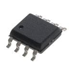
| 产品图片 |
|
| rohs | 符合RoHS无铅 / 符合限制有害物质指令(RoHS)规范要求 |
| 产品系列 | 校验器 IC,ON Semiconductor LM2903DG- |
| 数据手册 | |
| 产品型号 | LM2903DG |
| PCN组件/产地 | |
| 产品目录页面 | |
| 产品种类 | 模拟比较器 |
| 传播延迟(最大值) | - |
| 供应商器件封装 | 8-SOIC N |
| 偏转电压—最大值 | 7 mV |
| 元件数 | 2 |
| 其它名称 | LM2903DG-ND |
| 包装 | 管件 |
| 响应时间 | 1.5 us |
| 商标 | ON Semiconductor |
| 安装类型 | 表面贴装 |
| 安装风格 | SMD/SMT |
| 封装 | Tube |
| 封装/外壳 | 8-SOIC(0.154",3.90mm 宽) |
| 封装/箱体 | SOIC-8 |
| 工作温度 | -40°C ~ 125°C |
| 工厂包装数量 | 98 |
| 最大功率耗散 | 570 mW |
| 最大工作温度 | + 105 C |
| 最小工作温度 | - 40 C |
| 标准包装 | 98 |
| 滞后 | - |
| 电压-电源,单/双 (±) | 2 V ~ 36 V, ±1 V ~ 18 V |
| 电压-输入失调(最大值) | 7mV @ 30V |
| 电压增益dB | 106.02 dB |
| 电流-输入偏置(最大值) | 0.25µA @ 5V |
| 电流-输出(典型值) | 16mA @ 5V |
| 电流-静态(最大值) | 2.5mA |
| 电源电压-最大 | 36 V |
| 电源电压-最小 | 2 V |
| 电源电流 | 1 mA |
| 电源电流—最大值 | 1 mA |
| 类型 | 通用 |
| 系列 | LM2903 |
| 输入偏压电流—最大 | 250 nA |
| 输出电流—典型值 | 16 mA |
| 输出类型 | Open Collector |
| 通道数量 | 2 Channel |


- 商务部:美国ITC正式对集成电路等产品启动337调查
- 曝三星4nm工艺存在良率问题 高通将骁龙8 Gen1或转产台积电
- 太阳诱电将投资9.5亿元在常州建新厂生产MLCC 预计2023年完工
- 英特尔发布欧洲新工厂建设计划 深化IDM 2.0 战略
- 台积电先进制程称霸业界 有大客户加持明年业绩稳了
- 达到5530亿美元!SIA预计今年全球半导体销售额将创下新高
- 英特尔拟将自动驾驶子公司Mobileye上市 估值或超500亿美元
- 三星加码芯片和SET,合并消费电子和移动部门,撤换高东真等 CEO
- 三星电子宣布重大人事变动 还合并消费电子和移动部门
- 海关总署:前11个月进口集成电路产品价值2.52万亿元 增长14.8%


PDF Datasheet 数据手册内容提取
LM393, LM393E, LM293, LM2903, LM2903E, LM2903V, NCV2903 Low Offset Voltage Dual Comparators The LM393 series are dual independent precision voltage www.onsemi.com comparators capable of single or split supply operation. These devices are designed to permit a common mode range−to−ground level with single supply operation. Input offset voltage specifications as low as 2.0 mV make this device an excellent selection for many applications PDIP−8 in consumer, automotive, and industrial electronics. N SUFFIX 8 CASE 626 Features • 1 Wide Single−Supply Range: 2.0 Vdc to 36 Vdc • Split−Supply Range: ±1.0 Vdc to ±18 Vdc SOIC−8 D SUFFIX • Very Low Current Drain Independent of Supply Voltage: 0.4 mA 8 CASE 751 • Low Input Bias Current: 25 nA 1 • Low Input Offset Current: 5.0 nA Micro8(cid:2) • Low Input Offset Voltage: 5.0 mV (max) LM293/393 DM SUFFIX 8 • Input Common Mode Range to Ground Level 1 CASE 846A • Differential Input Voltage Range Equal to Power Supply Voltage • Output Voltage Compatible with DTL, ECL, TTL, MOS, and CMOS Logic Levels PIN CONNECTIONS • ESD Clamps on the Inputs Increase the Ruggedness of the Device without Affecting Performance Output A 1 8 VCC • NCV Prefix for Automotive and Other Applications Requiring 2 − 7 Output B Inputs A + 3 6 Unique Site and Control Change Requirements; AEC−Q100 GND4 −+ 5 Inputs B Qualified and PPAP Capable • These Devices are Pb−Free, Halogen Free/BFR Free and are RoHS (Top View) Compliant VCC + Input - Input Output DEVICE MARKING AND ORDERING INFORMATION See detailed marking information and ordering and shipping R2 information on pages 6 and 7 of this data sheet. 2.1 k Q4 R4 Q5 Q6 Q3 Q14 2.0 k F1 Q10 Q9 Q16 Q1 Q8 Q12 Q2 Q15 Q11 R1 4.6 k Figure 1. Representative Schematic Diagram (Diagram shown is for 1 comparator) © Semiconductor Components Industries, LLC, 2016 1 Publication Order Number: February, 2018 − Rev. 32 LM393/D
LM393, LM393E, LM293, LM2903, LM2903E, LM2903V, NCV2903 MAXIMUM RATINGS Rating Symbol Value Unit Power Supply Voltage VCC +36 or ±18 V Input Differential Voltage VIDR 36 V Input Common Mode Voltage Range VICR −0.3 to +36 V Output Voltage VO 36 V Output Short Circuit−to−Ground ISC Continuous mA Output Sink Current (Note 1) ISink 20 Power Dissipation @ TA = 25°C PD 570 mW Derate above 25°C 1/R(cid:2)JA 5.7 mW/°C Operating Ambient Temperature Range TA °C LM293 −25 to +85 LM393, LM393E 0 to +70 LM2903, LM2903E −40 to +105 LM2903V, NCV2903 (Note 2) −40 to +125 Maximum Operating Junction Temperature TJ(max) °C LM393, LM393E, LM2903, LM2903E, LM2903V 150 LM293, NCV2903 150 Storage Temperature Range Tstg −65 to +150 °C Stresses exceeding those listed in the Maximum Ratings table may damage the device. If any of these limits are exceeded, device functionality should not be assumed, damage may occur and reliability may be affected. 1. The maximum output current may be as high as 20 mA, independent of the magnitude of VCC, output short circuits to VCC can cause excessive heating and eventual destruction. 2. NCV2903 is qualified for automotive use. ESD RATINGS Rating HBM MM Unit ESD Protection at any Pin (Human Body Model − HBM, Machine Model − MM) NCV2903 (Note 2) 2000 200 V LM393E, LM2903E 1500 150 V LM393DG/DR2G, LM2903DG/DR2G 250 100 V All Other Devices 1500 150 V www.onsemi.com 2
LM393, LM393E, LM293, LM2903, LM2903E, LM2903V, NCV2903 ELECTRICAL CHARACTERISTICS (VCC = 5.0 Vdc, Tlow ≤TA ≤ Thigh, unless otherwise noted.) LM2903/E/V, LM293, LM393, LM393E NCV2903 Characteristic Symbol Min Typ Max Min Typ Max Unit Input Offset Voltage (Note 4) VIO mV TA = 25°C − ±1.0 ±5.0 − ±2.0 ±7.0 Tlow ≤TA ≤ Thigh − − ±9.0 − ±9.0 ±15 Input Offset Current IIO nA TA = 25°C − ±5.0 ±50 − ±5.0 ±50 Tlow ≤TA ≤ Thigh − − ±150 − ±50 ±200 Input Bias Current (Note 5) IIB nA TA = 25°C − 20 250 − 20 250 Tlow ≤TA ≤ Thigh − − 400 − 20 500 Input Common Mode Voltage Range (Note 6) VICR V TA = 25°C 0 − VCC −1.5 0 − VCC −1.5 Tlow ≤TA ≤ Thigh 0 − VCC −2.0 0 − VCC −2.0 Voltage Gain AVOL 50 200 − 25 200 − V/mV RL ≥ 15 k(cid:3), VCC = 15 Vdc, TA = 25°C Large Signal Response Time − − 300 − − 300 − ns Vin = TTL Logic Swing, Vref = 1.4 Vdc VRL = 5.0 Vdc, RL = 5.1 k(cid:3), TA = 25°C Response Time (Note 7) tTLH − 1.3 − − 1.5 − (cid:4)s VRL = 5.0 Vdc, RL = 5.1 k(cid:3), TA = 25°C Input Differential Voltage (Note 8) VID − − VCC − − VCC V All Vin ≥ GND or V− Supply (if used) Output Sink Current ISink 6.0 16 − 6.0 16 − mA Vin ≥ 1.0 Vdc, Vin+ = 0 Vdc, VO ≤ 1.5 Vdc TA = 25°C Output Saturation Voltage VOL mV Vin ≥ 1.0 Vdc, Vin+ = 0, ISink ≤ 4.0 mA, TA = 25°C − 150 400 − − 400 Tlow ≤TA ≤ Thigh − − 700 − 200 700 Output Leakage Current IOL nA Vin− = 0 V, Vin+ ≥ 1.0 Vdc, VO = 5.0 Vdc, TA = 25°C − 0.1 − − 0.1 − Vin− = 0 V, Vin+ ≥ 1.0 Vdc, VO = 30 Vdc, Tlow ≤TA ≤ Thigh − − 1000 − − 1000 Supply Current ICC mA RL = ∞ Both Comparators, TA = 25°C − 0.4 1.0 − 0.4 1.0 RL = ∞ Both Comparators, VCC = 30 V − − 2.5 − − 2.5 Product parametric performance is indicated in the Electrical Characteristics for the listed test conditions, unless otherwise noted. Product performance may not be indicated by the Electrical Characteristics if operated under different conditions. LM293 Tlow = −25°C, Thigh = +85°C LM393, LM393E Tlow = 0°C, Thigh = +70°C LM2903, LM2903E Tlow = −40°C, Thigh = +105°C LM2903V & NCV2903 Tlow = −40°C, Thigh = +125°C NCV2903 is qualified for automotive use. 3. The maximum output current may be as high as 20 mA, independent of the magnitude of VCC, output short circuits to VCC can cause excessive heating and eventual destruction. 4. At output switch point, VO(cid:2)1.4 Vdc, RS = 0 (cid:3) with VCC from 5.0 Vdc to 30 Vdc, and over the full input common mode range (0 V to VCC = −1.5 V). 5. Due to the PNP transistor inputs, bias current will flow out of the inputs. This current is essentially constant, independent of the output state, therefore, no loading changes will exist on the input lines. 6. Input common mode of either input should not be permitted to go more than 0.3 V negative of ground or minus supply. The upper limit of common mode range is VCC −1.5 V. 7. Response time is specified with a 100 mV step and 5.0 mV of overdrive. With larger magnitudes of overdrive faster response times are obtainable. 8. The comparator will exhibit proper output state if one of the inputs becomes greater than VCC, the other input must remain within the common mode range. The low input state must not be less than −0.3 V of ground or minus supply. www.onsemi.com 3
LM393, LM393E, LM293, LM2903, LM2903E, LM2903V, NCV2903 LM293/393 LM2903 25 14 TA = 0°C TA = -40°C TA = 0°C TA = -40°C CURRENT (nA) 2213 TA = +25°C CURRENT (nA) 111123 TTAA = = + +2750°°CC S 19 S BIA TA = +125°C BIA 10 NPUT 17 TA = +105°C NPUT 9 TA = +125°C I , IIB 15 TA = +70°C TA = +85°C I , IIB 8 TA = +85°C TA = +105°C 13 7 0 5 10 15 20 25 30 35 40 0 5 10 15 20 25 30 35 40 VCC, SUPPLY VOLTAGE (Vdc) VCC, SUPPLY VOLTAGE (Vdc) Figure 2. Input Bias Current versus Figure 3. Input Bias Current versus Power Supply Voltage Power Supply Voltage 10 10 Out of Out of c) c) d Saturation d Saturation V V E ( E ( G 1.0 G 1.0 A A LT TA = +125°C LT VO VO TA = +85°C N N O O RATI 0.1 TA = +25°C TA = -55° C RATI 0.1 TA = +25° C U U T T A A S S V , OL0.01 V , OL0.01 TA = 0°C TA = -40°C 0.001 0.001 0.01 0.1 1.0 10 100 0.01 0.1 1.0 10 100 ISink, OUTPUT SINK CURRENT (mA) ISink, OUTPUT SINK CURRENT (mA) Figure 4. Output Saturation Voltage Figure 5. Output Saturation Voltage versus Output Sink Current versus Output Sink Current 1.0 mA) TA = -55° C A) 1.2 TA = -40° C RENT ( 0.8 TTAA == 0+°2 5C° C ENT (m 1.0 TA = 0° C R R PLY CU 0.6 TA = +70°C LY CUR 0.8 TA = +25° C P P I , SUCC 00..42 RL = (cid:3)TA = +125°C I , SUPCC 0.6 RL = (cid:3)TA = +85° C 0.4 0 5.0 10 15 20 25 30 35 40 0 5.0 10 15 20 25 30 35 40 VCC, SUPPLY VOLTAGE (Vdc) VCC, SUPPLY VOLTAGE (Vdc) Figure 6. Power Supply Current versus Figure 7. Power Supply Current versus Power Supply Voltage Power Supply Voltage www.onsemi.com 4
LM393, LM393E, LM293, LM2903, LM2903E, LM2903V, NCV2903 APPLICATIONS INFORMATION These dual comparators feature high gain, wide The addition of positive feedback (<10mV) is also bandwidth characteristics. This gives the device oscillation recommended. It is good design practice to ground all tendencies if the outputs are capacitively coupled to the unused pins. inputs via stray capacitance. This oscillation manifests Differential input voltages may be larger than supply itself during output transitions (V to V ). To alleviate voltage without damaging the comparator’s inputs. Voltages OL OH this situation, input resistors <10 k(cid:3) should be used. more negative than −0.3 V should not be used. +15 V 8R.21 k 22R04 k 22R05 k 10 k Vin Vin(min) (cid:5) Vin R1 6.8 k LM393 D1 R2 (cid:8) +VCC (cid:6) (cid:5) 10 k 15 k 10 m LM393 R3 Vin (cid:8) VCC D1 prevents input from going negative by more than 0.6 V. VO (cid:6) -VEE (cid:5)(cid:6) R1 + R2 = R3 - VEE R5 R3 ≤ for small error in zero crossing. 10 Vin(min) (cid:4) 0.4 V peak for 1% phase distortion ((cid:5)(cid:6)). Figure 8. Zero Crossing Detector Figure 9. Zero Crossing Detector (Single Supply) (Split Supply) VCC VCC 1.0 m(cid:3) VCC t R RL + - RL LM393 LM393 - 10 k VCC 0.001 (cid:4)F LM393 - VC C + VO VO + + Vref 51 k ``ON'' for t (cid:6) tO + (cid:5)t where: Vin Vref 51 k 51 k VVCOC (cid:5)t = RC (cid:7) n ( VVCreCf ) VO00 0 VC0 Vref t tO (cid:7) t Figure 10. Free−Running Square−Wave Oscillator Figure 11. Time Delay Generator VCC RS = R1 | | R2 RS RL - (VCC -Vref) R1 LM393 Vth1 = Vref + R1 + R2 + RL + (Vref -VO Low) R1 R1 Vth2 = Vref - R1 + R2 Vref R2 Figure 12. Comparator with Hysteresis www.onsemi.com 5
LM393, LM393E, LM293, LM2903, LM2903E, LM2903V, NCV2903 MARKING DIAGRAMS PDIP−8 Micro8 CASE 626 CASE 846A 8 8 8 8 8 x93 2903 903V LM393NG LM2903N AWL AWL AYW(cid:2) AYW(cid:2) AYW(cid:2) YYWW YYWWG (cid:2) (cid:2) (cid:2) 1 1 1 1 1 SOIC−8 CASE 751 8 8 8 LMx93 2903 * 2903V ALYW ALYW ALYW (cid:2) (cid:2) (cid:2) 1 1 1 8 8 393E 2903E ALYW ALYW (cid:2) (cid:2) 1 1 x = 2 or 3 A = Assembly Location WL, L = Wafer Lot YY, Y = Year WW, W = Work Week (cid:2), G = Pb−Free Package (Note: Microdot may be in either location) *This marking diagram also applies to NCV2903DR2G www.onsemi.com 6
LM393, LM393E, LM293, LM2903, LM2903E, LM2903V, NCV2903 ORDERING INFORMATION Operating Temperature Device Range Package Shipping† LM293DG 98 Units / Rail SOIC−8 LM293DR2G (Pb−Free) 2500 / Tape & Reel −25°C to +85°C LM293DMR2G Micro8 4000 / Tape and Reel (Pb−Free) LM393DG 98 Units / Rail SOIC−8 LM393DR2G (Pb−Free) 2500 / Tape & Reel LM393EDR2G SOIC−8 2500 / Tape & Reel (Pb−Free) 0°C to +70°C LM393NG PDIP−8 50 Units / Rail (Pb−Free) LM393DMR2G Micro8 4000 / Tape and Reel (Pb−Free) LM2903DG 98 Units / Rail SOIC−8 LM2903DR2G (Pb−Free) 2500 / Tape & Reel LM2903EDR2G SOIC−8 2500 / Tape & Reel (Pb−Free) −40°C to +105°C LM2903DMR2G Micro8 4000 / Tape and Reel (Pb−Free) LM2903NG PDIP−8 50 Units / Rail (Pb−Free) LM2903VDG 98 Units / Rail SOIC−8 LM2903VDR2G (Pb−Free) 2500 / Tape & Reel LM2903VNG PDIP−8 50 Units / Rail (Pb−Free) −40°C to +125°C NCV2903DR2G* SOIC−8 2500 / Tape & Reel (Pb−Free) NCV2903DMR2G* Micro8 4000 / Tape & Reel (Pb−Free) †For information on tape and reel specifications, including part orientation and tape sizes, please refer to our Tape and Reel Packaging Specifications Brochure, BRD8011/D. *NCV Prefix for Automotive and Other Applications Requiring Unique Site and Control Change Requirements; AEC−Q100 Qualified and PPAP Capable. www.onsemi.com 7
LM393, LM393E, LM293, LM2903, LM2903E, LM2903V, NCV2903 PACKAGE DIMENSIONS PDIP−8 N, AN, VN SUFFIX CASE 626−05 ISSUE P D A NOTES: 1. DIMENSIONING AND TOLERANCING PER ASME Y14.5M, 1994. E 2. CONTROLLING DIMENSION: INCHES. H 3. DIMENSIONS A, A1 AND L ARE MEASURED WITH THE PACK- AGE SEATED IN JEDEC SEATING PLANE GAUGE GS−3. 8 5 4. DIMENSIONS D, D1 AND E1 DO NOT INCLUDE MOLD FLASH OR PROTRUSIONS. MOLD FLASH OR PROTRUSIONS ARE E1 NOT TO EXCEED 0.10 INCH. 5. DIMENSION E IS MEASURED AT A POINT 0.015 BELOW DATUM PLANE H WITH THE LEADS CONSTRAINED PERPENDICULAR 1 4 TO DATUM C. 6. DIMENSION eB IS MEASURED AT THE LEAD TIPS WITH THE NOTE 8 c LEADS UNCONSTRAINED. b2 B 7. DATUM PLANE H IS COINCIDENT WITH THE BOTTOM OF THE END VIEW LEADS, WHERE THE LEADS EXIT THE BODY. TOP VIEW WITH LEADS CONSTRAINED 8. PACKAGE CONTOUR IS OPTIONAL (ROUNDED OR SQUARE CORNERS). NOTE 5 INCHES MILLIMETERS A2 DIM MIN MAX MIN MAX e/2 A A −−−− 0.210 −−− 5.33 NOTE 3 A1 0.015 −−−− 0.38 −−− A2 0.115 0.195 2.92 4.95 L b 0.014 0.022 0.35 0.56 b2 0.060 TYP 1.52 TYP C 0.008 0.014 0.20 0.36 D 0.355 0.400 9.02 10.16 SEATING A1 PLANE D1 0.005 −−−− 0.13 −−− E 0.300 0.325 7.62 8.26 C M E1 0.240 0.280 6.10 7.11 D1 e 0.100 BSC 2.54 BSC e eB eB −−−− 0.430 −−− 10.92 L 0.115 0.150 2.92 3.81 8Xb END VIEW M −−−− 10° −−− 10° 0.010 M C A M B M NOTE 6 SIDE VIEW www.onsemi.com 8
LM393, LM393E, LM293, LM2903, LM2903E, LM2903V, NCV2903 PACKAGE DIMENSIONS SOIC−8 NB CASE 751−07 ISSUE AK NOTES: −X− 1. DIMENSIONING AND TOLERANCING PER ANSI Y14.5M, 1982. A 2. CONTROLLING DIMENSION: MILLIMETER. 3. DIMENSION A AND B DO NOT INCLUDE MOLD PROTRUSION. 4. MAXIMUM MOLD PROTRUSION 0.15 (0.006) 8 5 PER SIDE. 5. DIMENSION D DOES NOT INCLUDE DAMBAR B S 0.25 (0.010) M Y M PROTRUSION. ALLOWABLE DAMBAR PROTRUSION SHALL BE 0.127 (0.005) TOTAL 1 IN EXCESS OF THE D DIMENSION AT −Y− 4 K 6. 7M5A1X−I0M1U TMH RMUA T7E51R−IA0L6 CAROEN DOIBTSIOONL.ETE. NEW STANDARD IS 751−07. G MILLIMETERS INCHES DIM MIN MAX MIN MAX A 4.80 5.00 0.189 0.197 C NX 45(cid:3) B 3.80 4.00 0.150 0.157 SEATING C 1.35 1.75 0.053 0.069 PLANE D 0.33 0.51 0.013 0.020 −Z− G 1.27 BSC 0.050 BSC H 0.10 0.25 0.004 0.010 0.10 (0.004) J 0.19 0.25 0.007 0.010 H D M J K 0.40 1.27 0.016 0.050 M 0 (cid:3) 8 (cid:3) 0 (cid:3) 8 (cid:3) N 0.25 0.50 0.010 0.020 0.25 (0.010)M Z Y S X S S 5.80 6.20 0.228 0.244 SOLDERING FOOTPRINT* 1.52 0.060 7.0 4.0 0.275 0.155 0.6 1.270 0.024 0.050 (cid:9) (cid:10) mm SCALE 6:1 inches *For additional information on our Pb−Free strategy and soldering details, please download the ON Semiconductor Soldering and Mounting Techniques Reference Manual, SOLDERRM/D. www.onsemi.com 9
LM393, LM393E, LM293, LM2903, LM2903E, LM2903V, NCV2903 PACKAGE DIMENSIONS Micro8(cid:4) CASE 846A−02 ISSUE J DD NOTES: 1. DIMENSIONING AND TOLERANCING PER ANSI Y14.5M, 1982. 2. CONTROLLING DIMENSION: MILLIMETER. 3. DIMENSION A DOES NOT INCLUDE MOLD FLASH, PROTRUSIONS OR GATE BURRS. MOLD FLASH, PROTRUSIONS OR GATE BURRS SHALL NOT EXCEED 0.15 (0.006) PER SIDE. HE E 4. DIMENSION B DOES NOT INCLUDE INTERLEAD FLASH OR PROTRUSION. INTERLEAD FLASH OR PROTRUSION SHALL NOT EXCEED 0.25 (0.010) PER SIDE. 5. 846A-01 OBSOLETE, NEW STANDARD 846A-02. MILLIMETERS INCHES DIM MIN NOM MAX MIN NOM MAX PIN 1 ID e A −− −− 1.10 −− −− 0.043 b8 PL A1 0.05 0.08 0.15 0.002 0.003 0.006 b 0.25 0.33 0.40 0.010 0.013 0.016 0.08 (0.003) M T B S A S c 0.13 0.18 0.23 0.005 0.007 0.009 D 2.90 3.00 3.10 0.114 0.118 0.122 E 2.90 3.00 3.10 0.114 0.118 0.122 e 0.65 BSC 0.026 BSC SEATING L 0.40 0.55 0.70 0.016 0.021 0.028 −T− PLANE HE 4.75 4.90 5.05 0.187 0.193 0.199 0.038 (0.0015) A A1 c L RECOMMENDED SOLDERING FOOTPRINT* 8X 8X0.48 0.80 5.25 0.65 PITCH DIMENSION: MILLIMETERS *For additional information on our Pb−Free strategy and soldering details, please download the ON Semiconductor Soldering and Mounting Techniques Reference Manual, SOLDERRM/D. Micro8 is a trademark of International Rectifier. ON Semiconductor and are trademarks of Semiconductor Components Industries, LLC dba ON Semiconductor or its subsidiaries in the United States and/or other countries. ON Semiconductor owns the rights to a number of patents, trademarks, copyrights, trade secrets, and other intellectual property. A listing of ON Semiconductor’s product/patent coverage may be accessed at www.onsemi.com/site/pdf/Patent−Marking.pdf. ON Semiconductor reserves the right to make changes without further notice to any products herein. ON Semiconductor makes no warranty, representation or guarantee regarding the suitability of its products for any particular purpose, nor does ON Semiconductor assume any liability arising out of the application or use of any product or circuit, and specifically disclaims any and all liability, including without limitation special, consequential or incidental damages. Buyer is responsible for its products and applications using ON Semiconductor products, including compliance with all laws, regulations and safety requirements or standards, regardless of any support or applications information provided by ON Semiconductor. “Typical” parameters which may be provided in ON Semiconductor data sheets and/or specifications can and do vary in different applications and actual performance may vary over time. All operating parameters, including “Typicals” must be validated for each customer application by customer’s technical experts. ON Semiconductor does not convey any license under its patent rights nor the rights of others. ON Semiconductor products are not designed, intended, or authorized for use as a critical component in life support systems or any FDA Class 3 medical devices or medical devices with a same or similar classification in a foreign jurisdiction or any devices intended for implantation in the human body. Should Buyer purchase or use ON Semiconductor products for any such unintended or unauthorized application, Buyer shall indemnify and hold ON Semiconductor and its officers, employees, subsidiaries, affiliates, and distributors harmless against all claims, costs, damages, and expenses, and reasonable attorney fees arising out of, directly or indirectly, any claim of personal injury or death associated with such unintended or unauthorized use, even if such claim alleges that ON Semiconductor was negligent regarding the design or manufacture of the part. ON Semiconductor is an Equal Opportunity/Affirmative Action Employer. This literature is subject to all applicable copyright laws and is not for resale in any manner. PUBLICATION ORDERING INFORMATION LITERATURE FULFILLMENT: N. American Technical Support: 800−282−9855 Toll Free ON Semiconductor Website: www.onsemi.com Literature Distribution Center for ON Semiconductor USA/Canada 19521 E. 32nd Pkwy, Aurora, Colorado 80011 USA Europe, Middle East and Africa Technical Support: Order Literature: http://www.onsemi.com/orderlit Phone: 303−675−2175 or 800−344−3860 Toll Free USA/Canada Phone: 421 33 790 2910 Fax: 303−675−2176 or 800−344−3867 Toll Free USA/Canada For additional information, please contact your local Email: orderlit@onsemi.com Sales Representative ◊ www.onsemi.com LM393/D 10
Mouser Electronics Authorized Distributor Click to View Pricing, Inventory, Delivery & Lifecycle Information: O N Semiconductor: NCV2903DMR2G NCV2903DR2G LM2903DG LM2903DMR2G LM2903DR2G LM2903NG LM2903VDG LM2903VDR2G LM293DG LM293DMR2G LM293DR2G LM393DG LM393DMR2G LM393DR2G LM393NG