ICGOO在线商城 > 集成电路(IC) > PMIC - 稳压器 - DC DC 开关稳压器 > LM2831YMF/NOPB

 Datasheet下载
- 型号: LM2831YMF/NOPB
- 制造商: Texas Instruments
- 库位|库存: xxxx|xxxx
- 要求:
| 数量阶梯 | 香港交货 | 国内含税 |
| +xxxx | $xxxx | ¥xxxx |
查看当月历史价格
查看今年历史价格
LM2831YMF/NOPB产品简介:
ICGOO电子元器件商城为您提供LM2831YMF/NOPB由Texas Instruments设计生产,在icgoo商城现货销售,并且可以通过原厂、代理商等渠道进行代购。 LM2831YMF/NOPB价格参考¥6.63-¥14.99。Texas InstrumentsLM2831YMF/NOPB封装/规格:PMIC - 稳压器 - DC DC 开关稳压器, 可调式 降压 开关稳压器 IC 正 0.6V 1 输出 1.5A SC-74A,SOT-753。您可以下载LM2831YMF/NOPB参考资料、Datasheet数据手册功能说明书,资料中有LM2831YMF/NOPB 详细功能的应用电路图电压和使用方法及教程。
Texas Instruments(德州仪器)的LM2831YMF/NOPB是一款高效的同步降压DC-DC开关稳压器,广泛应用于需要高效、紧凑电源解决方案的场景中。以下是该型号的主要应用场景:

 1. 便携式电子设备
   LM2831YMF/NOPB常用于便携式电子设备中,如智能手机、平板电脑、智能手表等。这些设备对电源效率和尺寸要求极高,而LM2831YMF/NOPB的高集成度和小封装能够满足其需求。它可以在低功耗模式下提供稳定的电压输出,延长电池续航时间。

 2. 工业控制系统
   在工业自动化和控制系统中,LM2831YMF/NOPB可以为传感器、微控制器和其他低功耗组件提供稳定的电源。其宽输入电压范围(2.95V至6V)使其能够适应不同的电源输入条件,确保系统的稳定运行。

 3. 通信设备
   对于无线通信模块、路由器、调制解调器等设备,LM2831YMF/NOPB能够提供高效且稳定的电源管理。它支持快速瞬态响应,能够在负载变化时保持输出电压的稳定性,确保通信信号的质量。

 4. 消费类电子产品
   在消费类电子产品中,如蓝牙耳机、智能家居设备等,LM2831YMF/NOPB的应用也非常广泛。它的小尺寸和高效能使得产品设计更加灵活,同时降低了功耗,提升了用户体验。

 5. 医疗设备
   在便携式医疗设备中,如血糖仪、心率监测器等,LM2831YMF/NOPB可以提供稳定的电源,确保设备的准确性和可靠性。其低噪声特性也有助于减少对敏感电路的干扰。

 6. 汽车电子
   在汽车电子系统中,如车载信息娱乐系统、传感器模块等,LM2831YMF/NOPB可以为各种低功耗组件提供稳定的电源。其宽工作温度范围(-40°C至+85°C)使其能够在恶劣的环境中可靠工作。

 总结
LM2831YMF/NOPB凭借其高效、紧凑的设计,适用于多种应用场景,尤其是在对电源效率、尺寸和稳定性有较高要求的便携式设备、工业控制、通信设备、消费类电子产品、医疗设备以及汽车电子等领域中表现出色。
| 参数 | 数值 |
| 产品目录 | 集成电路 (IC)半导体 |
| 描述 | IC REG BUCK ADJ 1.5A SOT23-5稳压器—开关式稳压器 HI FREQ 1.5A LOAD- STEP DOWN DC-DC REG |
| 产品分类 | |
| 品牌 | Texas Instruments |
| 产品手册 | |
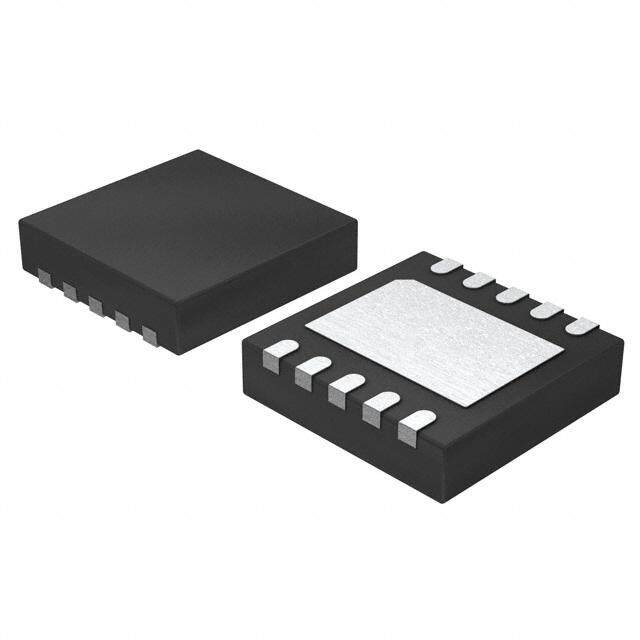
| 产品图片 |
|
| rohs | 符合RoHS无铅 / 符合限制有害物质指令(RoHS)规范要求 |
| 产品系列 | 电源管理 IC,稳压器—开关式稳压器,Texas Instruments LM2831YMF/NOPB- |
| 数据手册 | |
| 产品型号 | LM2831YMF/NOPB |
| PWM类型 | 电流模式 |
| 产品目录页面 | |
| 产品种类 | 稳压器—开关式稳压器 |
| 供应商器件封装 | SOT-23-5 |
| 其它名称 | *LM2831YMF/NOPB |
| 包装 | 剪切带 (CT) |
| 同步整流器 | 无 |
| 商标 | Texas Instruments |
| 安装类型 | 表面贴装 |
| 安装风格 | SMD/SMT |
| 封装 | Reel |
| 封装/外壳 | SC-74A,SOT-753 |
| 封装/箱体 | SOT-23 |
| 工作温度 | -40°C ~ 125°C |
| 工厂包装数量 | 1000 |
| 开关频率 | 550 kHz |
| 最大工作温度 | + 125 C |
| 最大输入电压 | 5.5 V |
| 最小工作温度 | - 40 C |
| 最小输入电压 | 3 V |
| 标准包装 | 1 |
| 电压-输入 | 3 V ~ 5.5 V |
| 电压-输出 | 0.6 V ~ 4.5 V |
| 电流-输出 | 1.5A |
| 类型 | 降压(降压) |
| 系列 | LM2831 |
| 输出数 | 1 |
| 输出电压 | 0.6 V to 4.5 V |
| 输出电流 | 1.5 A |
| 输出端数量 | 1 Output |
| 输出类型 | 可调式 |
| 配用 | /product-detail/zh/LM2831YMF%20EVAL/LM2831YMF%20EVAL-ND/1640629 |
| 频率-开关 | 550kHz |


- 商务部:美国ITC正式对集成电路等产品启动337调查
- 曝三星4nm工艺存在良率问题 高通将骁龙8 Gen1或转产台积电
- 太阳诱电将投资9.5亿元在常州建新厂生产MLCC 预计2023年完工
- 英特尔发布欧洲新工厂建设计划 深化IDM 2.0 战略
- 台积电先进制程称霸业界 有大客户加持明年业绩稳了
- 达到5530亿美元!SIA预计今年全球半导体销售额将创下新高
- 英特尔拟将自动驾驶子公司Mobileye上市 估值或超500亿美元
- 三星加码芯片和SET,合并消费电子和移动部门,撤换高东真等 CEO
- 三星电子宣布重大人事变动 还合并消费电子和移动部门
- 海关总署:前11个月进口集成电路产品价值2.52万亿元 增长14.8%


PDF Datasheet 数据手册内容提取
Product Sample & Technical Tools & Support & Reference Folder Buy Documents Software Community Design LM2831 SNVS422D–AUGUST2006–REVISEDSEPTEMBER2015 LM2831 High-Frequency 1.5-A Load — Step-Down DC-DC Regulator 1 Features 3 Description • Space-SavingSOT-23Package The LM2831 regulator is a monolithic, high- 1 frequency, PWM step-down DC-DC converter in a 5- • InputVoltageRangeof3Vto5.5V pin SOT-23 and a 6-Pin WSON package. The • OutputVoltageRangeof0.6Vto4.5V LM2831 provides all the active functions to provide • 1.5-AOutputCurrent local DC-DC conversion with fast transient response and accurate regulation in the smallest possible PCB • HighSwitchingFrequencie area. With a minimum of external components, the – 1.6MHz(LM2831X) LM2831 is easy to use. The ability to drive 1.5-A – 0.55MHz(LM2831Y) loads with an internal 130-mΩ PMOS switch using state-of-the-art 0.5-µm BiCMOS technology results in – 3MHz(LM2831Z) the best power density available. The world-class • 130-mΩ PMOSSwitch control circuitry allows on-times as low as 30 ns, thus • 0.6-V,2%InternalVoltageReference supporting exceptionally high frequency conversion • InternalSoftStart over the entire 3 V to 5.5 V input operating range, down to the minimum output voltage of 0.6 V. • CurrentMode,PWMOperation Switching frequency is internally set to 550 kHz, 1.6 • ThermalShutdown MHz, or 3 MHz, allowing the use of extremely small • OvervoltageProtection surface mount inductors and chip capacitors. Even though the operating frequency is high, efficiencies of 2 Applications up to 93% are easy to achieve. External shutdown is included, featuring an ultra-low standby current of 30 • Local5VtoVcoreStep-DownConverters nA. The LM2831 utilizes current-mode control and • CorePowerinHDDs internal compensation to provide high-performance regulation over a wide range of operating conditions. • Set-TopBoxes Additional features include internal soft-start circuitry • USBPoweredDevices to reduce inrush current, pulse-by-pulse current limit, • DSLModems thermalshutdown,andoutputovervoltageprotection. DeviceInformation(1) PARTNUMBER PACKAGE BODYSIZE(NOM) WSON(6) 3.00mm×3.00mm LM2831 SOT-23(5) 1.60mm×2.90mm (1) For all available packages, see the orderable addendum at theendofthedatasheet. TypicalApplicationCircuit EfficiencyvsLoad EN FB 100 LM2831 GND R3 VIN SW L1 VO = 3.3V @ 1.5A "X" VIN = 5V R1 90 C1 D1 C2 C3 R2 %) ( 80 Y C N E CI FI 70 F E 60 50 0.1 1 LOAD (A) 1 An IMPORTANT NOTICE at the end of this data sheet addresses availability, warranty, changes, use in safety-critical applications, intellectualpropertymattersandotherimportantdisclaimers.PRODUCTIONDATA.
LM2831 SNVS422D–AUGUST2006–REVISEDSEPTEMBER2015 www.ti.com Table of Contents 1 Features.................................................................. 1 7.4 DeviceFunctionalModes........................................11 2 Applications........................................................... 1 8 ApplicationandImplementation........................ 12 3 Description............................................................. 1 8.1 ApplicationInformation............................................12 4 RevisionHistory..................................................... 2 8.2 TypicalApplications ...............................................12 5 PinConfigurationandFunctions......................... 3 9 PowerSupplyRecommendations...................... 25 6 Specifications......................................................... 4 10 Layout................................................................... 25 6.1 AbsoluteMaximumRatings......................................4 10.1 LayoutGuidelines.................................................25 6.2 ESDRatings..............................................................4 10.2 LayoutExample....................................................29 6.3 RecommendedOperatingConditions.......................4 11 DeviceandDocumentationSupport................. 30 6.4 ThermalInformation..................................................4 11.1 DeviceSupport......................................................30 6.5 ElectricalCharacteristics...........................................5 11.2 DocumentationSupport........................................30 6.6 TypicalCharacteristics..............................................6 11.3 CommunityResources..........................................30 7 DetailedDescription.............................................. 9 11.4 Trademarks...........................................................30 7.1 Overview...................................................................9 11.5 ElectrostaticDischargeCaution............................30 7.2 FunctionalBlockDiagram.........................................9 11.6 Glossary................................................................30 7.3 FeatureDescription...................................................9 12 Mechanical,Packaging,andOrderable Information........................................................... 30 4 Revision History NOTE:Pagenumbersforpreviousrevisionsmaydifferfrompagenumbersinthecurrentversion. ChangesfromRevisionC(April2013)toRevisionD Page • AddedESDRatingstable,FeatureDescriptionsection,DeviceFunctionalModes,ApplicationandImplementation section,PowerSupplyRecommendationssection,Layoutsection,DeviceandDocumentationSupportsection,and Mechanical,Packaging,andOrderableInformationsection. ................................................................................................ 1 ChangesfromRevisionB(April2013)toRevisionC Page • ChangedlayoutofNationalDataSheettoTIformat........................................................................................................... 24 2 SubmitDocumentationFeedback Copyright©2006–2015,TexasInstrumentsIncorporated ProductFolderLinks:LM2831
LM2831 www.ti.com SNVS422D–AUGUST2006–REVISEDSEPTEMBER2015 5 Pin Configuration and Functions NGGPackage 6-PinsWSON TopView FB 1 6 EN GND 2 DAP 5 VINA SW 3 4 VIND DBVPackage 5-PinSOT-23 TopView EN 4 3 FB 2 GND VIN 5 1 SW PinFunctions PIN I/O DESCRIPTION NAME SOT-23 WSON Enablecontrolinput.Logichighenablesoperation.Donotallowthispinto EN 4 6 I floatorbegreaterthanV +0.3V,orV +0.3VforWSON. IN INA FB 3 1 I Feedbackpin.Connecttoexternalresistordividertosetoutputvoltage. Signalandpowergroundpin.Placethebottomresistorofthefeedback GND 2 2 PWR networkascloseaspossibletothispin. SW 1 3 O Outputswitch.Connecttotheinductorandcatchdiode. VIN 5 — PWR Inputsupplyvoltage VINA — 5 PWR Controlcircuitrysupplyvoltage.ConnectVINAtoVINDonPCboard. VIND — 4 PWR Powerinputsupply DieAttach Connecttosystemgroundforlowthermalimpedance,butitcannotbe — DAP PWR Pad usedasaprimaryGNDconnection. Copyright©2006–2015,TexasInstrumentsIncorporated SubmitDocumentationFeedback 3 ProductFolderLinks:LM2831
LM2831 SNVS422D–AUGUST2006–REVISEDSEPTEMBER2015 www.ti.com 6 Specifications 6.1 Absolute Maximum Ratings overoperatingfree-airtemperaturerange(unlessotherwisenoted)(1)(2) MIN MAX UNIT V –0.5 7 V IN FBVoltage –0.5 3 V ENVoltage –0.5 7 V SWVoltage –0.5 7 V JunctionTemperature(3) 150 °C SolderingInformation InfraredorConvectionReflow(15sec) 220 °C StorageTemperature,T –65 150 °C stg (1) StressesbeyondthoselistedunderAbsoluteMaximumRatingsmaycausepermanentdamagetothedevice.Thesearestressratings only,whichdonotimplyfunctionaloperationofthedeviceattheseoranyotherconditionsbeyondthoseindicatedunderRecommended OperatingConditions.Exposuretoabsolute-maximum-ratedconditionsforextendedperiodsmayaffectdevicereliability. (2) IfMilitary/Aerospacespecifieddevicesarerequired,pleasecontacttheTexasInstrumentsSalesOffice/Distributorsforavailabilityand specifications. (3) Thermalshutdownwilloccurifthejunctiontemperatureexceedsthemaximumjunctiontemperatureofthedevice. 6.2 ESD Ratings VALUE UNIT V Electrostaticdischarge Humanbodymodel(HBM),perANSI/ESDA/JEDECJS-001(1) ±2000 V (ESD) (1) JEDECdocumentJEP155statesthat500-VHBMallowssafemanufacturingwithastandardESDcontrolprocess. 6.3 Recommended Operating Conditions overoperatingfree-airtemperaturerange(unlessotherwisenoted) MIN NOM MAX UNIT V 3 5.5 V IN JunctionTemperature –40 125 °C 6.4 Thermal Information LM2831 THERMALMETRIC(1) SOT-23(DBV WSON(NGG) UNIT 5PINS 6PINS R Junction-to-ambientthermalresistance(2) 163.4 54.9 °C/W θJA R Junction-to-case(top)thermalresistance(2) 114.4 50.8 °C/W θJC(top) R Junction-to-boardthermalresistance 26.8 29.2 °C/W θJB ψ Junction-to-topcharacterizationparameter 12.4 0.6 °C/W JT ψ Junction-to-boardcharacterizationparameter 26.2 29.3 °C/W JB R Junction-to-case(bottom)thermalresistance N/A 9.2 °C/W θJC(bot) (1) Formoreinformationabouttraditionalandnewthermalmetrics,seetheSemiconductorandICPackageThermalMetricsapplication report,SPRA953. (2) Appliesforpackagessoldereddirectlyontoa3”×3”PCboardwith2oz.copperon4layersinstillair. 4 SubmitDocumentationFeedback Copyright©2006–2015,TexasInstrumentsIncorporated ProductFolderLinks:LM2831
LM2831 www.ti.com SNVS422D–AUGUST2006–REVISEDSEPTEMBER2015 6.5 Electrical Characteristics V =5VunlessotherwiseindicatedundertheTestConditionscolumn.LimitsareforT =25°C.MinimumandMaximum IN J limitsarespecifiedthroughtest,design,orstatisticalcorrelation.Typicalvaluesrepresentthemostlikelyparametricnormat T =25°C,andareprovidedforreferencepurposesonly. J PARAMETER TESTCONDITIONS MIN TYP MAX UNIT WSONandSOT-23 TJ=25°C 0.600 VFB FeedbackVoltage Package V –40°Cto125°C 0.588 0.612 ΔVFB/VIN FeedbackVoltageLineRegulation VIN=3Vto5V 0.02 %/V IB FeedbackInputBiasCurrent TJ=25°C 0.1 nA –40°Cto125°C 100 VINRising TJ=25°C 2.73 V –40°Cto125°C 2.90 UndervoltageLockout UVLO VINFalling TJ=25°C 2.3 V –40°Cto125°C 1.85 UVLOHysteresis 0.43 V LM2831-X TJ=25°C 1.6 –40°Cto125°C 1.2 1.95 LM2831-Y TJ=25°C 0.55 FSW SwitchingFrequency MHz –40°Cto125°C 0.4 0.7 LM2831-Z TJ=25°C 3 –40°Cto125°C 2.25 3.75 LM2831-X TJ=25°C 94% –40°Cto125°C 86% LM2831-Y TJ=25°C 96% DMAX MaximumDutyCycle –40°Cto125°C 90% LM2831-Z TJ=25°C 90% –40°Cto125°C 82% LM2831-X 5% DMIN MinimumDutyCycle LM2831-Y 2% LM2831-Z 7% WSONPackage 150 RDS(ON) SwitchOnResistance SOT-23Package TJ=25°C 130 mΩ –40°Cto125°C 195 ICL SwitchCurrentLimit VIN=3.3V TJ=25°C 2.5 A –40°Cto125°C 1.8 ShutdownThresholdVoltage –40°Cto125°C 0.4 VEN_TH V EnableThresholdVoltage –40°Cto125°C 1.8 ISW SwitchLeakage 100 nA IEN EnablePinCurrent Sink/Source 100 nA LM2831XVFB=0.55 TJ=25°C 3.3 –40°Cto125°C 5 LM2831YVFB=0.55 TJ=25°C 2.8 QuiescentCurrent(switching) mA IQ –40°Cto125°C 4.5 LM2831ZVFB=0.55 TJ=25°C 4.3 –40°Cto125°C 6.5 QuiescentCurrent(shutdown) AllOptionsVEN=0V 30 nA TSD ThermalShutdownTemperature 165 °C Copyright©2006–2015,TexasInstrumentsIncorporated SubmitDocumentationFeedback 5 ProductFolderLinks:LM2831
LM2831 SNVS422D–AUGUST2006–REVISEDSEPTEMBER2015 www.ti.com 6.6 Typical Characteristics AllcurvestakenatV =5VwithconfigurationintypicalapplicationcircuitshowninApplicationInformationsectionofthis IN datasheet.T =25°C,unlessotherwisespecified. J 1.804 1.803 1.802 V) 1.801 T ( U 1.800 P T U O 1.799 1.798 1.797 1.796 0 0.25 0.5 0.75 1 1.25 1.5 LOAD (A) VIN=3.3 VO=1.8V VIN=3.3V VO=1.8V(AllOptions) Figure1.ηvsLoad–X,Y,andZOptions Figure2.LoadRegulation 1.806 3.302 1.804 3.301 1.802 V) V) 3.300 T ( T ( U 1.800 U P P T T OU OU 3.299 1.798 3.298 1.796 1.794 3.297 0 0.25 0.5 0.75 1 1.25 1.5 0 0.25 0.5 0.75 1 1.25 1.5 LOAD (A) LOAD (A) V =5V V =1.8V(AllOptions) V =5V V =3.3V(AllOptions) IN O IN O Figure3.LoadRegulation Figure4.LoadRegulation 0.60 1.81 )z 1.76 )zH 0.58 H M M( Y 1.71 ( YC 0.56 C N N 1.66 E E U U Q 0.54 Q 1.61 E E R R F F R 1.56 RO 0.52 O T TAL 1.51 ALL 0.50 LIC 1.46 ICS S O O 0.48 1.41 1.36 0.46 -45 -40 -10 20 50 80 110 125 130 -45 -40 -10 20 50 80 110 125 130 TEMPERATURE (ºC) TEMPERATURE (ºC) Figure5.OscillatorFrequencyvsTemperature–XOption Figure6.OscillatorFrequencyvsTemperature–YOption 6 SubmitDocumentationFeedback Copyright©2006–2015,TexasInstrumentsIncorporated ProductFolderLinks:LM2831
LM2831 www.ti.com SNVS422D–AUGUST2006–REVISEDSEPTEMBER2015 Typical Characteristics (continued) AllcurvestakenatV =5VwithconfigurationintypicalapplicationcircuitshowninApplicationInformationsectionofthis IN datasheet.T =25°C,unlessotherwisespecified. J 3.45 2900 )z 3.35 2800 H M 3.25 ( YCNEUQ 33..0155 MIT (mA) 22760000 ER T LI 2500 F ROTALL 22..9855 CURREN 22340000 IC 2.75 S O 2200 2.65 2100 2.55 -45 -40 -10 20 50 80 110 125 130 -45 -40 -10 20 50 80 110 125 130 TEMPERATURE (ºC) TEMPERATURE (°C) V =3.3V IN Figure7.OscillatorFrequencyvsTemperature–ZOption Figure8.CurrentLimitvsTemperature Figure9.RDSONvsTemperature(WSONPackage) Figure10.RDSONvsTemperature(SOT-23Package) 3.6 2.65 2.6 3.5 2.55 2.5 3.4 2.45 A) )A I (mQ 3.3 m( IQ 2.4 2.35 3.2 2.3 3.1 2.25 2.2 3.0 2.15 -45 -40 -10 20 50 80 110 125 130 -45 -40 -10 20 50 80 110 125 130 TEMPERATURE (ºC) TEMPERATURE (°C) Figure11.LM2831XIQ(QuiescentCurrent) Figure12.LM2831YIQ(QuiescentCurrent) Copyright©2006–2015,TexasInstrumentsIncorporated SubmitDocumentationFeedback 7 ProductFolderLinks:LM2831
LM2831 SNVS422D–AUGUST2006–REVISEDSEPTEMBER2015 www.ti.com Typical Characteristics (continued) AllcurvestakenatV =5VwithconfigurationintypicalapplicationcircuitshowninApplicationInformationsectionofthis IN datasheet.T =25°C,unlessotherwisespecified. J 4.6 4.5 4.4 A) m 4.3 (Q I 4.2 4.1 4.0 -45 -40 -10 20 50 80 110 125 130 TEMPERATURE (ºC) V =1.8V I =500mA O O Figure13.LM2831ZI (QuiescentCurrent) Figure14.LineRegulation Q 0.610 )V 0.605 ( E G A T L OV 0.600 K C A B E EF 0.595 0.590 -45 -40 -10 20 50 80 110 125 130 TEMPERATURE (ºC) V =5V V =1.2Vat1A IN O Figure15.VFBvsTemperature Figure16.GainvsFrequency V =5V V =1.2Vat1A IN O Figure17.PhasePlotvsFrequency 8 SubmitDocumentationFeedback Copyright©2006–2015,TexasInstrumentsIncorporated ProductFolderLinks:LM2831
LM2831 www.ti.com SNVS422D–AUGUST2006–REVISEDSEPTEMBER2015 7 Detailed Description 7.1 Overview The LM2831 device is a constant-frequency PWM buck regulator IC that delivers a 1.5-A load current. The regulator has a preset switching frequency of 550 kHz, 1.6 MHz, or 3 MHz. This high-frequency allows the LM2831 to operate with small surface mount capacitors and inductors, resulting in a DC-DC converter that requires a minimum amount of board space. The LM2831 is internally compensated, so the device is simple to useandrequiresfewexternalcomponents. 7.2 Functional Block Diagram EN VIN + I SENSE - ENABLE and UVLO Thermal + - SHDN I LIMIT OVP SHDN - + 1.15 xV REF RampArtificial Control Logic cv S R I (cid:14) SENSE (cid:14) 1.6 MHz + FB - R Q PFET - + DRIVER Internal-Comp SW VREF = 0.6V SOFT-START Internal-LDO GND 7.3 Feature Description 7.3.1 TheoryofOperation The LM2831 uses current-mode control to regulate the output voltage. The following operating description of the LM2831 will refer to Functional Block Diagram and to the waveforms in Figure 18. The LM2831 supplies a regulated output voltage by switching the internal PMOS control switch at constant-frequency and variable duty cycle. A switching cycle begins at the falling edge of the reset pulse generated by the internal oscillator. When this pulse goes low, the output control logic turns on the internal PMOS control switch. During this on-time, the SW pin voltage (V ) swings up to approximately V , and the inductor current (I ) increases with a linear slope. SW IN L I is measured by the current sense amplifier, which generates an output proportional to the switch current. The L sense signal is summed with the regulator’s corrective ramp and compared to the error amplifier’s output, which Copyright©2006–2015,TexasInstrumentsIncorporated SubmitDocumentationFeedback 9 ProductFolderLinks:LM2831
LM2831 SNVS422D–AUGUST2006–REVISEDSEPTEMBER2015 www.ti.com Feature Description (continued) isproportionaltothedifferencebetweenthefeedbackvoltageandV .WhenthePWMcomparatoroutputgoes REF high, the output switch turns off until the next switching cycle begins. During the switch off-time, inductor current discharges through the Schottky catch diode, which forces the SW pin to swing below ground by the forward voltage (V ) of the Schottky catch diode. The regulator loop adjusts the duty cycle (D) to maintain a constant D outputvoltage. VSW D=TON/TSW VIN SW Voltage TON TOFF 0 VD t TSW IL IPK Inductor Current 0 t Figure18. TypicalWaveforms 7.3.2 SoftStart This function forces V to increase at a controlled rate during start up. During soft start, the error amplifier’s OUT reference voltage ramps from 0 V to its nominal value of 0.6 V in approximately 600 µs. This forces the regulator outputtorampupinacontrolledfashion,whichhelpsreduceinrushcurrent. 7.3.3 OutputOvervoltageProtection The overvoltage comparator compares the FB pin voltage to a voltage that is 15% higher than the internal reference V . Once the FB pin voltage goes 15% above the internal reference, the internal PMOS control REF switchisturnedoff,whichallowstheoutputvoltagetodecreasetowardregulation. 7.3.4 UndervoltageLockout Undervoltage lockout (UVLO) prevents the LM2831 from operating until the input voltage exceeds 2.73 V (typical). The UVLO threshold has approximately 430 mV of hysteresis, so the part will operate until V drops IN below2.3V(typical).HysteresispreventsthepartfromturningoffduringpowerupifV isnon-monotonic. IN 7.3.5 CurrentLimit The LM2831 uses cycle-by-cycle current limiting to protect the output switch. During each switching cycle, a current limit comparator detects if the output switch current exceeds 2.5 A (typical), and turns off the switch until thenextswitchingcyclebegins. 7.3.6 ThermalShutdown Thermal shutdown limits total power dissipation by turning off the output switch when the IC junction temperature exceeds 165°C. After thermal shutdown occurs, the output switch doesn’t turn on until the junction temperature dropstoapproximately150°C. 10 SubmitDocumentationFeedback Copyright©2006–2015,TexasInstrumentsIncorporated ProductFolderLinks:LM2831
LM2831 www.ti.com SNVS422D–AUGUST2006–REVISEDSEPTEMBER2015 7.4 Device Functional Modes The LM2831 has an enable pin (EN) control Input. A logic high enables device operation. Do not float this pin or let this pin be greater than VIN + 0.3 V for the SOT package option, or VINA + 0.3 V for the WSON package option. Copyright©2006–2015,TexasInstrumentsIncorporated SubmitDocumentationFeedback 11 ProductFolderLinks:LM2831
LM2831 SNVS422D–AUGUST2006–REVISEDSEPTEMBER2015 www.ti.com 8 Application and Implementation NOTE Information in the following applications sections is not part of the TI component specification, and TI does not warrant its accuracy or completeness. TI’s customers are responsible for determining suitability of components for their purposes. Customers should validateandtesttheirdesignimplementationtoconfirmsystemfunctionality. 8.1 Application Information The LM2831 device will operate with input voltage range from 3 V to 5.5 V and provide a regulated output voltage. This device is optimized for high-efficiency operation with minimum number of external components. For componentselection,seeDetailedDesignProcedure. 8.2 Typical Applications 8.2.1 LM2831XDesignExample1 EN FB GND LM2831 R3 L1 V = 1.2V @ 1.5A VIN SW O V = 5V IN R1 C1 D1 C2 R2 Figure19. LM2831X(1.6MHz):V =5V,V =1.2Vat1.5A IN O 8.2.1.1 DesignRequirements The device must be able to operate at any voltage within the recommended operating range. Load current must be defined to properly size the inductor, input, and output capacitors. Inductor should be able to handle full expected load current as well as the peak current generated during load transients and start up. Inrush current at start-upwilldependontheoutputcapacitorselection.MoredetailsareprovidedinDetailedDesignProcedure. 12 SubmitDocumentationFeedback Copyright©2006–2015,TexasInstrumentsIncorporated ProductFolderLinks:LM2831
LM2831 www.ti.com SNVS422D–AUGUST2006–REVISEDSEPTEMBER2015 Typical Applications (continued) 8.2.1.2 DetailedDesignProcedure Table1.BillofMaterials PARTID PARTVALUE MANUFACTURER PARTNUMBER U1 1.5-ABuckRegulator TI LM2831X C1,InputCap 22µF,6.3V,X5R TDK C3216X5ROJ226M C2,OutputCap 2x22µF,6.3V,X5R TDK C3216X5ROJ226M D1,CatchDiode 0.3V Schottky1.5A,30V TOSHIBA CRS08 f R L1 3.3µH,2.2A TDK VLCF5020T-3R3N2R0-1 R2 15.0kΩ,1% Vishay CRCW08051502F R1 15.0kΩ,1% Vishay CRCW08051502F R3 100kΩ,1% Vishay CRCW08051003F 8.2.1.2.1 InductorSelection Thedutycycle(D)canbeapproximatedquicklyusingtheratioofoutputvoltage(V )toinputvoltage(V ): O IN V D = OUT V IN (1) The catch diode (D1) forward voltage drop and the voltage drop across the internal PMOS must be included to calculateamoreaccuratedutycycle.CalculateDbyusingthefollowingformula: V +V D = OUT D V +V -V IN D SW (2) V canbeapproximatedby: SW V =I ×R (3) SW OUT DSON The diode forward drop (V ) can range from 0.3 V to 0.7 V depending on the quality of the diode. The lower the D V , the higher the operating efficiency of the converter. The inductor value determines the output ripple current. D Lowerinductorvaluesdecreasethesizeoftheinductor,butincreasetheoutputripplecurrent.Anincreaseinthe inductorvaluewilldecreasetheoutputripplecurrent. One must ensure that the minimum current limit (1.8 A) is not exceeded, so the peak current in the inductor must becalculated.Thepeakcurrent(I )intheinductoriscalculatedby: LPK I =I +Δi (4) LPK OUT L ’i L I OUT V V -V OUT IN OUT L L DT T t S S Figure20. InductorCurrent V -V 2Di IN OUT = L L DT S (5) Copyright©2006–2015,TexasInstrumentsIncorporated SubmitDocumentationFeedback 13 ProductFolderLinks:LM2831
LM2831 SNVS422D–AUGUST2006–REVISEDSEPTEMBER2015 www.ti.com Ingeneral, Δi =0.1×(I )→0.2×(I ) (6) L OUT OUT If Δi = 20% of 1.50 A, the peak current in the inductor will be 1.8 A. The minimum ensured current limit over all L operating conditions is 1.8 A. One can either reduce Δi , or make the engineering judgment that zero margin will L besafeenough.Thetypicalcurrentlimitis2.5A. The LM2831 operates at frequencies allowing the use of ceramic output capacitors without compromising transient response. Ceramic capacitors allow higher inductor ripple without significantly increasing output ripple. SeetheOutputCapacitorsectionformoredetailsoncalculatingoutput voltage ripple. Now that the ripple current isdetermined,theinductanceiscalculatedby: æDT ö L =ç S ÷´V -V IN OUT 2Di è L ø (7) Where: 1 T = S f S (8) When selecting an inductor, make sure that it is capable of supporting the peak output current without saturating. Inductor saturation will result in a sudden reduction in inductance and prevent the regulator from operating correctly. Because of the speed of the internal current limit, the peak current of the inductor need only be specified for the required maximum output current. For example, if the designed maximum output current is 1 A and the peak current is 1.25 A, then the inductor should be specified with a saturation current limit of > 1.25 A. There is no need to specify the saturation or peak current of the inductor at the 2.5-A typical switch current limit. The difference in inductor size is a factor of 5. Because of the operating frequency of the LM2831, ferrite based inductors are preferred to minimize core losses. This presents little restriction since the variety of ferrite-based inductorsishuge.Lastly,inductorswithlowerseriesresistance(R )willprovidebetteroperatingefficiency.For DCR recommended inductors, see LM2831X Design Example 2 through LM2831X Buck Converter and Voltage DoubleCircuitWithLDOFollowerDesignExample9. 8.2.1.2.2 InputCapacitor An input capacitor is necessary to ensure that V does not drop excessively during switching transients. The IN primary specifications of the input capacitor are capacitance, voltage, RMS current rating, and ESL (Equivalent Series Inductance). The recommended input capacitance is 22 µF. The input voltage rating is specifically stated by the capacitor manufacturer. Make sure to check any recommended deratings and also verify if there is any significant change in capacitance at the operating input voltage and the operating temperature. The input capacitormaximumRMSinputcurrentrating(I )mustbegreaterthan: RMS-IN é Di2ù I DêI 2 (1-D)+ ú RMS_IN OUT êë 3 úû (9) Neglectinginductorripplesimplifiestheaboveequationto: I =I ´ D(1-D) RMS_IN OUT (10) It can be shown from the above equation that maximum RMS capacitor current occurs when D = 0.5. Always calculate the RMS at the point where the duty cycle D is closest to 0.5. The ESL of an input capacitor is usually determined by the effective cross sectional area of the current path. A large leaded capacitor will have high ESL and a 0805 ceramic chip capacitor will have very low ESL. At the operating frequencies of the LM2831, leaded capacitors may have an ESL so large that the resulting impedance (2πfL) will be higher than that required to providestableoperation.Asaresult,surfacemountcapacitorsarestronglyrecommended. Sanyo POSCAP, Tantalum or Niobium, Panasonic SP, and multilayer ceramic capacitors (MLCC) are all good choices for both input and output capacitors and have very low ESL. For MLCCs it is recommended to use X7R or X5R type capacitors due to their tolerance and temperature characteristics. Consult capacitor manufacturer datasheetstoseehowratedcapacitancevariesoveroperatingconditions. 14 SubmitDocumentationFeedback Copyright©2006–2015,TexasInstrumentsIncorporated ProductFolderLinks:LM2831
LM2831 www.ti.com SNVS422D–AUGUST2006–REVISEDSEPTEMBER2015 8.2.1.2.3 OutputCapacitor The output capacitor is selected based upon the desired output ripple and transient response. The initial current ofaloadtransientisprovidedmainlybytheoutputcapacitor.Theoutputrippleoftheconverteris: æ 1 ö V = DI çR + ÷ OUT L ESR 8´F ´C è SW OUT ø (11) When using MLCCs, the ESR is typically so low that the capacitive ripple may dominate. When this occurs, the output ripple will be approximately sinusoidal and 90° phase shifted from the switching action. Given the availabilityandqualityofMLCCsandtheexpectedoutputvoltageofdesignsusingtheLM2831,thereisreallyno need to review any other capacitor technologies. Another benefit of ceramic capacitors is their ability to bypass high frequency noise. A certain amount of switching edge noise will couple through parasitic capacitances in the inductor to the output. A ceramic capacitor will bypass this noise while a tantalum will not. Since the output capacitor is one of the two external components that control the stability of the regulator control loop, most applications will require a minimum of 22 µF of output capacitance. Capacitance often, but not always, can be increased significantly with little detriment to the regulator stability. Like the input capacitor, recommended multilayerceramiccapacitorsareX7RorX5Rtypes. 8.2.1.2.4 CatchDiode The catch diode (D1) conducts during the switch off-time. A Schottky diode is recommended for its fast switching timesandlowforwardvoltagedrop.Thecatchdiodeshouldbechosensothatitscurrentratingisgreaterthan: I =I ×(1-D) (12) D1 OUT The reverse breakdown rating of the diode must be at least the maximum input voltage plus appropriate margin. Toimproveefficiency,chooseaSchottkydiodewithalowforwardvoltagedrop. 8.2.1.2.5 OutputVoltage The output voltage is set using the following equation where R2 is connected between the FB pin and GND, and R1 is connected between V and the FB pin. A good value for R2 is 10 kΩ. When designing a unity gain O converter(Vo=0.6V),R1shouldbefrom0Ω to100Ω,andR2shouldbeequalorgreaterthan10kΩ. V OUT R1 = - 1 x R2 V REF (13) V =0.60V (14) REF Copyright©2006–2015,TexasInstrumentsIncorporated SubmitDocumentationFeedback 15 ProductFolderLinks:LM2831
LM2831 SNVS422D–AUGUST2006–REVISEDSEPTEMBER2015 www.ti.com 8.2.1.3 ApplicationCurves SeeTypicalCharacteristics. V =5V V =1.8Vand3.3V V =5V V =1.8Vand3.3V IN O IN O Figure21.ηvsLoad–XOption Figure22.ηvsLoad–YOption V =5V V =1.8Vand3.3V IN O Figure23.ηvsLoad–ZOption 16 SubmitDocumentationFeedback Copyright©2006–2015,TexasInstrumentsIncorporated ProductFolderLinks:LM2831
LM2831 www.ti.com SNVS422D–AUGUST2006–REVISEDSEPTEMBER2015 8.2.2 LM2831XDesignExample2 EN FB GND LM2831 R3 VIN SW L1 VO = 0.6V @ 1.5A VIN = 5V R1 C1 D1 C2 R2 Figure24. LM2831X(1.6MHz):V =5V,V =0.6Vat1.5A IN O Table2.BillofMaterials PARTID PARTVALUE MANUFACTURER PARTNUMBER U1 1.5-ABuckRegulator TI LM2831X C1,InputCapacitor 22µF,6.3V,X5R TDK C3216X5ROJ226M C2,OutputCapacitor 2x22µF,6.3V,X5R TDK C3216X5ROJ226M D1,CatchDiode 0.3V Schottky1.5A,30V TOSHIBA CRS08 f R L1 3.3µH,2.2A TDK VLCF5020T-3R3N2R0-1 R2 10.0kΩ,1% Vishay CRCW08051000F R1 0Ω R3 100kΩ,1% Vishay CRCW08051003F Copyright©2006–2015,TexasInstrumentsIncorporated SubmitDocumentationFeedback 17 ProductFolderLinks:LM2831
LM2831 SNVS422D–AUGUST2006–REVISEDSEPTEMBER2015 www.ti.com 8.2.3 LM2831XDesignExample3 EN FB GND LM2831 R3 VIN SW L1 VO = 3.3V @ 1.5A VIN = 5V R1 C1 D1 C2 R2 Figure25. LM2831X(1.6MHz):V =5V,V =3.3Vat1.5A IN O Table3.BillofMaterials PARTID PARTVALUE MANUFACTURER PARTNUMBER U1 1.5-ABuckRegulator TI LM2831X C1,InputCap 22µF,6.3V,X5R TDK C3216X5ROJ226M C2,OutputCap 2x22µF,6.3V,X5R TDK C3216X5ROJ226M D1,CatchDiode 0.3V Schottky1.5A,30V TOSHIBA CRS08 f R L1 2.7µH2.3A TDK VLCF5020T-2R7N2R2-1 R2 10.0kΩ,1% Vishay CRCW08051002F R1 45.3kΩ,1% Vishay CRCW08054532F R3 100kΩ,1% Vishay CRCW08051003F 18 SubmitDocumentationFeedback Copyright©2006–2015,TexasInstrumentsIncorporated ProductFolderLinks:LM2831
LM2831 www.ti.com SNVS422D–AUGUST2006–REVISEDSEPTEMBER2015 8.2.4 LM2831YDesignExample4 EN FB GND LM2831 R3 VIN SW L1 VO = 3.3V @ 1.5A VIN = 5V R1 C1 D1 C2 R2 Figure26. LM2831Y(550kHz):V =5V,V =3.3Vat1.5A IN OUT Table4.BillofMaterials PARTID PARTVALUE MANUFACTURER PARTNUMBER U1 1.5-ABuckRegulator TI LM2831Y C1,InputCap 22µF,6.3V,X5R TDK C3216X5ROJ226M C2,OutputCap 2x22µF,6.3V,X5R TDK C3216X5ROJ226M D1,CatchDiode 0.3V Schottky1.5A,30V TOSHIBA CRS08 f R L1 4.7µH2.1A TDK SLF7045T-4R7M2R0-PF R1 45.3kΩ,1% Vishay CRCW080545K3FKEA R2 10.0kΩ,1% Vishay CRCW08051002F Copyright©2006–2015,TexasInstrumentsIncorporated SubmitDocumentationFeedback 19 ProductFolderLinks:LM2831
LM2831 SNVS422D–AUGUST2006–REVISEDSEPTEMBER2015 www.ti.com 8.2.5 LM2831YDesignExample5 EN FB GND LM2831 R3 L1 V = 1.2V @ 1.5A VIN SW O V = 5V IN R1 C1 D1 C2 R2 Figure27. LM2831Y(550kHz):V =5V,V =1.2Vat1.5A IN OUT Table5.BillofMaterials PARTID PARTVALUE MANUFACTURER PARTNUMBER U1 1.5-ABuckRegulator TI LM2831Y C1,InputCap 22µF,6.3V,X5R TDK C3216X5ROJ226M C2,OutputCap 2x22µF,6.3V,X5R TDK C3216X5ROJ226M D1,CatchDiode 0.3V Schottky1.5A,30V TOSHIBA CRS08 f R L1 6.8µH1.8A TDK SLF7045T-6R8M1R7 R1 10.0kΩ,1% Vishay CRCW08051002F R2 10.0kΩ,1% Vishay CRCW08051002F 20 SubmitDocumentationFeedback Copyright©2006–2015,TexasInstrumentsIncorporated ProductFolderLinks:LM2831
LM2831 www.ti.com SNVS422D–AUGUST2006–REVISEDSEPTEMBER2015 8.2.6 LM2831ZDesignExample6 EN FB GND LM2831 R3 VIN SW L1 VO = 3.3V @ 1.5A VIN = 5V R1 C1 D1 C2 R2 Figure28. LM2831Z(3MHz):V =5V,V =3.3Vat1.5A IN O Table6.BillofMaterials PARTID PARTVALUE MANUFACTURER PARTNUMBER U1 1.5-ABuckRegulator TI LM2831Z C1,InputCap 22µF,6.3V,X5R TDK C3216X5ROJ226M C2,OutputCap 2x22µF,6.3V,X5R TDK C3216X5ROJ226M D1,CatchDiode 0.3V Schottky1.5A,30V TOSHIBA CRS08 f R L1 1.6µH2.0A TDK VLCF4018T-1R6N1R7-2 R2 10.0kΩ,1% Vishay CRCW08051002F R1 45.3kΩ,1% Vishay CRCW08054532F R3 100kΩ,1% Vishay CRCW08051003F Copyright©2006–2015,TexasInstrumentsIncorporated SubmitDocumentationFeedback 21 ProductFolderLinks:LM2831
LM2831 SNVS422D–AUGUST2006–REVISEDSEPTEMBER2015 www.ti.com 8.2.7 LM2831ZDesignExample7 EN FB GND LM2831 R3 L1 V = 1.2V @ 1.5A VIN SW O V = 5V IN R1 C1 D1 C2 R2 Figure29. LM2831Z(3MHz):V =5V,V =1.2Vat1.5A IN O Table7.BillofMaterials PARTID PARTVALUE MANUFACTURER PARTNUMBER U1 1.5-ABuckRegulator TI LM2831Z C1,InputCap 22µF,6.3V,X5R TDK C3216X5ROJ226M C2,OutputCap 2x22µF,6.3V,X5R TDK C3216X5ROJ226M D1,CatchDiode 0.3V Schottky1.5A,30V TOSHIBA CRS08 f R L1 1.6µH,2.0A TDK VLCF4018T-1R6N1R7-2 R2 10.0kΩ,1% Vishay CRCW08051002F R1 10.0kΩ,1% Vishay CRCW08051002F R3 100kΩ,1% Vishay CRCW08051003F 22 SubmitDocumentationFeedback Copyright©2006–2015,TexasInstrumentsIncorporated ProductFolderLinks:LM2831
LM2831 www.ti.com SNVS422D–AUGUST2006–REVISEDSEPTEMBER2015 8.2.8 LM2831XDualConverterswithDelayedEnabledDesignExample8 VIN U1 C1 R3 VIND VINA L1 VO=3.3V@1.5A SW R1 EN LM2831 D1 C2 R2 GND FB U3 R6 4 3 LP3470M5X-3.08 LP3470 2 RESET 5 1 VIN C7 U2 C3 VIND VINA L2 VO=1.2V@1.5A SW R4 LM2831 D2 C4 EN R5 GND FB Figure30. LM2831X(1.6MHz):V =5V,V =1.2Vat1.5Aand3.3Vat1.5A IN O Table8.BillofMaterials PARTID PARTVALUE MANUFACTURER PARTNUMBER U1,U2 1.5-ABuckRegulator TI LM2831X U3 PoweronReset TI LP3470M5X-3.08 C1,C3InputCap 22µF,6.3V,X5R TDK C3216X5ROJ226M C2,C4OutputCap 2x22µF,6.3V,X5R TDK C3216X5ROJ226M C7 Trrdelaycapacitor TDK D1,D2CatchDiode 0.3V Schottky1.5A,30V TOSHIBA CRS08 f R L1,L2 3.3µH,2.2A TDK VLCF5020T-3R3N2R0-1 R2,R4,R5 10.0kΩ,1% Vishay CRCW08051002F R1,R6 45.3kΩ,1% Vishay CRCW08054532F R3 100kΩ,1% Vishay CRCW08051003F Copyright©2006–2015,TexasInstrumentsIncorporated SubmitDocumentationFeedback 23 ProductFolderLinks:LM2831
LM2831 SNVS422D–AUGUST2006–REVISEDSEPTEMBER2015 www.ti.com 8.2.9 LM2831XBuckConverterandVoltageDoubleCircuitWithLDOFollowerDesignExample9 VO = 5.0V @ 150mA L2 U2 LDO D2 C4 C5 U1 C6 C3 LM2831 L1 VIN = 5V VIND SW VINA GND R1 C1 VO = 3.3V @ 1.5A EN FB C2 D1 R2 Figure31. LM2831X(1.6MHz):V =5V,V =3.3Vat1.5AandLP2986-5.0at150mA IN O Table9.BillofMaterials PARTID PARTVALUE MANUFACTURER PARTNUMBER U1 1.5-ABuckRegulator TI LM2831X U2 200-mALDO TI LP2986-5.0 C1,InputCap 22µF,6.3V,X5R TDK C3216X5ROJ226M C2,OutputCap 22µF,6.3V,X5R TDK C3216X5ROJ226M C3–C6 2.2µF,6.3V,X5R TDK C1608X5R0J225M D1,CatchDiode 0.3V Schottky1.5A,30V TOSHIBA CRS08 f R D2 0.4V Schottky20V ,500mA ONSemi MBR0520 f R L2 10µH,800mA CoilCraft ME3220-103 L1 3.3µH,2.2A TDK VLCF5020T-3R3N2R0-1 R2 45.3kΩ,1% Vishay CRCW08054532F R1 10.0kΩ,1% Vishay CRCW08051002F 24 SubmitDocumentationFeedback Copyright©2006–2015,TexasInstrumentsIncorporated ProductFolderLinks:LM2831
LM2831 www.ti.com SNVS422D–AUGUST2006–REVISEDSEPTEMBER2015 9 Power Supply Recommendations The LM2831 device is designed to operate from various DC power supplies. The impedance of the input supply rail should be low enough that the input current transient does not cause a drop below the UVLO level. If the input supply is connected by using long wires, additional bulk capacitance may be required in addition to normal inputcapacitor. 10 Layout 10.1 Layout Guidelines When planning layout there are a few things to consider when trying to achieve a clean, regulated output. The most important consideration is the close coupling of the GND connections of the input capacitor and the catch diode D1. These ground ends should be close to one another and be connected to the GND plane with at least two through-holes. Place these components as close to the IC as possible. Next in importance is the location of the GND connection of the output capacitor, which should be near the GND connections of CIN and D1. There should be a continuous ground plane on the bottom layer of a two-layer board except under the switching node island.TheFBpinisahighimpedancenodeandcareshouldbetakentomaketheFBtraceshorttoavoidnoise pickup and inaccurate regulation. The feedback resistors should be placed as close as possible to the IC, with the GND of R1 placed as close as possible to the GND of the IC. The V trace to R2 should be routed away OUT from the inductor and any other traces that are switching. High AC currents flow through the V , SW and V IN OUT traces, so they should be as short and wide as possible. However, making the traces wide increases radiated noise, so the designer must make this trade-off. Radiated noise can be decreased by choosing a shielded inductor. The remaining components should also be placed as close as possible to the IC. See Application Note AN-1229SNVA054forfurtherconsiderationsandtheLM2831demoboardasanexampleofa4-layerlayout. 10.1.1 CalculatingEfficiencyandJunctionTemperature ThecompleteLM2831DC-DCconverterefficiencycanbecalculatedinthefollowingmanner. P OUT h= P IN (15) Or P OUT h= P +P OUT LOSS (16) Calculations for determining the most significant power losses are shown below. Other losses totaling less than 2%arenotdiscussed. Power loss (P ) is the sum of two basic types of losses in the converter: switching and conduction. LOSS Conduction losses usually dominate at higher output loads, whereas switching losses remain relatively fixed and dominateatloweroutputloads.Thefirststepindeterminingthelossesistocalculatethedutycycle(D): V +V D = OUT D V +V -V IN D SW (17) V isthevoltagedropacrosstheinternalPFETwhenitison,andisequalto: SW V =I ×R (18) SW OUT DSON V is the forward voltage drop across the Schottky catch diode. It can be obtained from the diode manufactures D Electrical Characteristics section. If the voltage drop across the inductor (V ) is accounted for, the equation DCR becomes: V + V + V OUT D DCR D = V + V + V - V IN D DCR SW (19) Theconductionlossesinthefree-wheelingSchottkydiodearecalculatedasfollows: P =V ×I ×(1-D) (20) DIODE D OUT Copyright©2006–2015,TexasInstrumentsIncorporated SubmitDocumentationFeedback 25 ProductFolderLinks:LM2831
LM2831 SNVS422D–AUGUST2006–REVISEDSEPTEMBER2015 www.ti.com Layout Guidelines (continued) Often this is the single most significant power loss in the circuit. Care should be taken to choose a Schottky diodethathasalowforwardvoltagedrop. Another significant external power loss is the conduction loss in the output inductor. The equation can be simplifiedto: P =I 2×R (21) IND OUT DCR TheLM2831conductionlossismainlyassociatedwiththeinternalPFET: 1 ’i 2 PCOND(cid:3)= (IOUT2 x D) 1 +3 x I L RDSON OUT (22) Iftheinductorripplecurrentisfairlysmall,theconductionlossescanbesimplifiedto: P =I 2×R ×D (23) COND OUT DSON Switching losses are also associated with the internal PFET. They occur during the switch on and off transition periods, where voltages and currents overlap resulting in power loss. The simplest means to determine this loss istoempiricallymeasuringtheriseandfalltimes(10%to90%)oftheswitchattheswitchnode. Switchingpowerlossiscalculatedasfollows: P =1/2(V ×I ×F ×T ) (24) SWR IN OUT SW RISE P =1/2(V ×I ×F ×T ) (25) SWF IN OUT SW FALL P =P +P (26) SW SWR SWF Anotherlossisthepowerrequiredforoperationoftheinternalcircuitry: P =I ×V (27) Q Q IN I isthequiescentoperatingcurrent,andistypicallyaround2.5mAforthe0.55-MHzfrequencyoption. Q Typicalapplicationpowerlossesare: Table10.PowerLossTabulation PARAMETER VALUE PARAMETER VALUE V 5V IN V 3.3V P 4.125W OUT OUT I 1.25A OUT V 0.45V P 188mW D DIODE F 550kHz SW I 2.5mA P 12.5mW Q Q T 4nS P 7mW RISE SWR T 4nS P 7mW FALL SWF R 150mΩ P 156mW DS(ON) COND IND 70mΩ P 110mW DCR IND D 0.667 P 481mW LOSS η 88% P 183mW INTERNAL ΣP +P +P +P +P =P (28) COND SW DIODE IND Q LOSS ΣP +P +P +P =P (29) COND SWF SWR Q INTERNAL P =183mW (30) INTERNAL 26 SubmitDocumentationFeedback Copyright©2006–2015,TexasInstrumentsIncorporated ProductFolderLinks:LM2831
LM2831 www.ti.com SNVS422D–AUGUST2006–REVISEDSEPTEMBER2015 10.1.2 ThermalDefinitions T Chipjunctiontemperature J T Ambienttemperature A R Thermalresistancefromchipjunctiontodevicecase θJC R Thermalresistancefromchipjunctiontoambientair θJA HeatintheLM2831duetointernalpowerdissipationisremovedthroughconductionand/orconvection. Conduction Heattransferoccursthroughcrosssectionalareasofmaterial.Dependingonthematerial,the transferofheatcanbeconsideredtohavepoortogoodthermalconductivityproperties(insulator vs.conductor). HeatTransfergoesas: Silicon→package→leadframe →PCB Convection: Heattransferisbymeansofairflow.Thiscouldbefromafanornaturalconvection.Natural convectionoccurswhenaircurrentsrisefromthehotdevicetocoolerair. Thermalimpedanceisdefinedas: DT R = q Power (31) Thermalimpedancefromthesiliconjunctiontotheambientairisdefinedas: T -T R = J A qJA Power (32) ThePCBsize,weightofcopperusedtoroutetracesandgroundplane,andnumberoflayerswithinthePCBcan greatly effect R . The type and number of thermal vias can also make a large difference in the thermal θJA impedance. Thermal vias are necessary in most applications. They conduct heat from the surface of the PCB to the ground plane. Four to six thermal vias should be placed under the exposed pad to the ground plane if the WSONpackageisused. Thermal impedance also depends on the thermal properties of the application operating conditions (Vin, Vo, Io, andsoforth),andthesurroundingcircuitry. 10.1.2.1 SiliconJunctionTemperatureDeterminationMethod1 To accurately measure the silicon temperature for a given application, two methods can be used. The first methodrequirestheusertoknowthethermalimpedanceofthesiliconjunctiontotopcasetemperature. Someclarificationmustbemadebeforewegoanyfurther. R isthethermalimpedancefromallsixsidesofanICpackagetosiliconjunction. θJC R isthethermalimpedancefromtopcasetothesiliconjunction. ΦJC In this data sheet we will use R so that it allows the user to measure top case temperature with a small ΦJC thermocoupleattachedtothetopcase. R is approximately 30°C/Watt for the 6-pin WSON package with the exposed pad. Knowing the internal ΦJC dissipation from the efficiency calculation given previously, and the case temperature, which can be empirically measuredonthebenchwehave: T -T R = J C FJC Power (33) Therefore: T =(R ×P )+T (34) j ΦJC LOSS C Fromthepreviousexample: T =(R ×P )+T (35) j ΦJC INTERNAL C T =30°C/W×0.189W+T (36) j C Copyright©2006–2015,TexasInstrumentsIncorporated SubmitDocumentationFeedback 27 ProductFolderLinks:LM2831
LM2831 SNVS422D–AUGUST2006–REVISEDSEPTEMBER2015 www.ti.com Thesecondmethodcangiveaveryaccuratesiliconjunctiontemperature. ThefirststepistodetermineR oftheapplication.TheLM2831hasovertemperatureprotectioncircuitry.When θJA the silicon temperature reaches 165°C, the device stops switching. The protection circuitry has a hysteresis of about 15°C. Once the silicon temperature has decreased to approximately 150°C, the device will start to switch again. Knowing this, the R for any application can be characterized during the early stages of the design one θJA may calculate the R by placing the PCB circuit into a thermal chamber. Raise the ambient temperature in the θJA given working application until the circuit enters thermal shutdown. If the SW-pin is monitored, it will be obvious when the internal PFET stops switching, indicating a junction temperature of 165°C. Knowing the internal power dissipation from the above methods, the junction temperature, and the ambient temperature R can be θJA determined. 165°C-Ta R = qJA P INTERNAL (37) Once this is determined, the maximum ambient temperature allowed for a desired junction temperature can be found. An example of calculating R for an application using the Texas Instruments LM2831 WSON demonstration θJA boardisshownbelow. The four layer PCB is constructed using FR4 with ½ oz copper traces. The copper ground plane is on the bottom layer. The ground plane is accessed by two vias. The board measures 3 cm × 3 cm. It was placed in an oven with no forced airflow. The ambient temperature was raised to 144°C, and at that temperature, the device went intothermalshutdown. Fromthepreviousexample: P =189mW (38) INTERNAL 165°C-144°C R = =111°C/W qJA 189mW (39) Ifthejunctiontemperaturewastobekeptbelow125°C,thentheambienttemperaturecouldnotgoabove109°C T -(R ×P )=T (40) j θJA LOSS A 125°C-(111°C/W×189mW)=104°C (41) 10.1.3 WSONPackage DieAttach Mold Compound Material Gold Wire Die Cu Exposed Exposed Die Contact Attach Pad Figure32. InternalWSONConnection For certain high power applications, the PCB land may be modified to a "dog bone" shape (see Figure 33). By increasingthesizeofgroundplane,andaddingthermalvias,theR fortheapplicationcanbereduced. θJA 28 SubmitDocumentationFeedback Copyright©2006–2015,TexasInstrumentsIncorporated ProductFolderLinks:LM2831
LM2831 www.ti.com SNVS422D–AUGUST2006–REVISEDSEPTEMBER2015 10.2 Layout Example FB 1 6 EN GND 2 GND 5 VINA PLANE SW 3 4 VIND Figure33. 6-LeadWSONPCBDogBoneLayout Copyright©2006–2015,TexasInstrumentsIncorporated SubmitDocumentationFeedback 29 ProductFolderLinks:LM2831
LM2831 SNVS422D–AUGUST2006–REVISEDSEPTEMBER2015 www.ti.com 11 Device and Documentation Support 11.1 Device Support 11.1.1 Third-PartyProductsDisclaimer TI'S PUBLICATION OF INFORMATION REGARDING THIRD-PARTY PRODUCTS OR SERVICES DOES NOT CONSTITUTE AN ENDORSEMENT REGARDING THE SUITABILITY OF SUCH PRODUCTS OR SERVICES OR A WARRANTY, REPRESENTATION OR ENDORSEMENT OF SUCH PRODUCTS OR SERVICES, EITHER ALONEORINCOMBINATIONWITHANYTIPRODUCTORSERVICE. 11.2 Documentation Support 11.2.1 RelatedDocumentation Forrelateddocumentation,seethefollowing: AN-1229SIMPLESWITCHER ® PCBLayoutGuidelines,SNVA054 11.3 Community Resources The following links connect to TI community resources. Linked contents are provided "AS IS" by the respective contributors. They do not constitute TI specifications and do not necessarily reflect TI's views; see TI's Terms of Use. TIE2E™OnlineCommunity TI'sEngineer-to-Engineer(E2E)Community.Createdtofostercollaboration amongengineers.Ate2e.ti.com,youcanaskquestions,shareknowledge,exploreideasandhelp solveproblemswithfellowengineers. DesignSupport TI'sDesignSupport QuicklyfindhelpfulE2Eforumsalongwithdesignsupporttoolsand contactinformationfortechnicalsupport. 11.4 Trademarks E2EisatrademarkofTexasInstruments. Allothertrademarksarethepropertyoftheirrespectiveowners. 11.5 Electrostatic Discharge Caution Thesedeviceshavelimitedbuilt-inESDprotection.Theleadsshouldbeshortedtogetherorthedeviceplacedinconductivefoam duringstorageorhandlingtopreventelectrostaticdamagetotheMOSgates. 11.6 Glossary SLYZ022—TIGlossary. Thisglossarylistsandexplainsterms,acronyms,anddefinitions. 12 Mechanical, Packaging, and Orderable Information The following pages include mechanical, packaging, and orderable information. This information is the most current data available for the designated devices. This data is subject to change without notice and revision of thisdocument.Forbrowser-basedversionsofthisdatasheet,refertotheleft-handnavigation. 30 SubmitDocumentationFeedback Copyright©2006–2015,TexasInstrumentsIncorporated ProductFolderLinks:LM2831
PACKAGE OPTION ADDENDUM www.ti.com 8-Oct-2015 PACKAGING INFORMATION Orderable Device Status Package Type Package Pins Package Eco Plan Lead/Ball Finish MSL Peak Temp Op Temp (°C) Device Marking Samples (1) Drawing Qty (2) (6) (3) (4/5) LM2831XMF/NOPB ACTIVE SOT-23 DBV 5 1000 Green (RoHS CU SN Level-1-260C-UNLIM -40 to 125 SKYB & no Sb/Br) LM2831XMFX/NOPB ACTIVE SOT-23 DBV 5 3000 Green (RoHS CU SN Level-1-260C-UNLIM -40 to 125 SKYB & no Sb/Br) LM2831XSD NRND WSON NGG 6 1000 TBD Call TI Call TI -40 to 125 L193B LM2831XSD/NOPB ACTIVE WSON NGG 6 1000 Green (RoHS CU SN Level-3-260C-168 HR -40 to 125 L193B & no Sb/Br) LM2831XSDX/NOPB ACTIVE WSON NGG 6 4500 Green (RoHS CU SN Level-3-260C-168 HR -40 to 125 L193B & no Sb/Br) LM2831YMF/NOPB ACTIVE SOT-23 DBV 5 1000 Green (RoHS CU SN Level-1-260C-UNLIM -40 to 125 SKZB & no Sb/Br) LM2831YMFX/NOPB ACTIVE SOT-23 DBV 5 3000 Green (RoHS CU SN Level-1-260C-UNLIM -40 to 125 SKZB & no Sb/Br) LM2831YSD/NOPB ACTIVE WSON NGG 6 1000 Green (RoHS CU SN Level-3-260C-168 HR -40 to 125 L194B & no Sb/Br) LM2831ZMF/NOPB ACTIVE SOT-23 DBV 5 1000 Green (RoHS CU SN Level-1-260C-UNLIM -40 to 125 SLAB & no Sb/Br) LM2831ZSD/NOPB ACTIVE WSON NGG 6 1000 Green (RoHS CU SN Level-3-260C-168 HR -40 to 125 L195B & no Sb/Br) (1) The marketing status values are defined as follows: ACTIVE: Product device recommended for new designs. LIFEBUY: TI has announced that the device will be discontinued, and a lifetime-buy period is in effect. NRND: Not recommended for new designs. Device is in production to support existing customers, but TI does not recommend using this part in a new design. PREVIEW: Device has been announced but is not in production. Samples may or may not be available. OBSOLETE: TI has discontinued the production of the device. (2) Eco Plan - The planned eco-friendly classification: Pb-Free (RoHS), Pb-Free (RoHS Exempt), or Green (RoHS & no Sb/Br) - please check http://www.ti.com/productcontent for the latest availability information and additional product content details. TBD: The Pb-Free/Green conversion plan has not been defined. Pb-Free (RoHS): TI's terms "Lead-Free" or "Pb-Free" mean semiconductor products that are compatible with the current RoHS requirements for all 6 substances, including the requirement that lead not exceed 0.1% by weight in homogeneous materials. Where designed to be soldered at high temperatures, TI Pb-Free products are suitable for use in specified lead-free processes. Pb-Free (RoHS Exempt): This component has a RoHS exemption for either 1) lead-based flip-chip solder bumps used between the die and package, or 2) lead-based die adhesive used between the die and leadframe. The component is otherwise considered Pb-Free (RoHS compatible) as defined above. Green (RoHS & no Sb/Br): TI defines "Green" to mean Pb-Free (RoHS compatible), and free of Bromine (Br) and Antimony (Sb) based flame retardants (Br or Sb do not exceed 0.1% by weight in homogeneous material) Addendum-Page 1
PACKAGE OPTION ADDENDUM www.ti.com 8-Oct-2015 (3) MSL, Peak Temp. - The Moisture Sensitivity Level rating according to the JEDEC industry standard classifications, and peak solder temperature. (4) There may be additional marking, which relates to the logo, the lot trace code information, or the environmental category on the device. (5) Multiple Device Markings will be inside parentheses. Only one Device Marking contained in parentheses and separated by a "~" will appear on a device. If a line is indented then it is a continuation of the previous line and the two combined represent the entire Device Marking for that device. (6) Lead/Ball Finish - Orderable Devices may have multiple material finish options. Finish options are separated by a vertical ruled line. Lead/Ball Finish values may wrap to two lines if the finish value exceeds the maximum column width. Important Information and Disclaimer:The information provided on this page represents TI's knowledge and belief as of the date that it is provided. TI bases its knowledge and belief on information provided by third parties, and makes no representation or warranty as to the accuracy of such information. Efforts are underway to better integrate information from third parties. TI has taken and continues to take reasonable steps to provide representative and accurate information but may not have conducted destructive testing or chemical analysis on incoming materials and chemicals. TI and TI suppliers consider certain information to be proprietary, and thus CAS numbers and other limited information may not be available for release. In no event shall TI's liability arising out of such information exceed the total purchase price of the TI part(s) at issue in this document sold by TI to Customer on an annual basis. Addendum-Page 2
PACKAGE MATERIALS INFORMATION www.ti.com 20-Dec-2016 TAPE AND REEL INFORMATION *Alldimensionsarenominal Device Package Package Pins SPQ Reel Reel A0 B0 K0 P1 W Pin1 Type Drawing Diameter Width (mm) (mm) (mm) (mm) (mm) Quadrant (mm) W1(mm) LM2831XMF/NOPB SOT-23 DBV 5 1000 178.0 8.4 3.2 3.2 1.4 4.0 8.0 Q3 LM2831XMFX/NOPB SOT-23 DBV 5 3000 178.0 8.4 3.2 3.2 1.4 4.0 8.0 Q3 LM2831XSD WSON NGG 6 1000 178.0 12.4 3.3 3.3 1.0 8.0 12.0 Q1 LM2831XSD/NOPB WSON NGG 6 1000 178.0 12.4 3.3 3.3 1.0 8.0 12.0 Q1 LM2831XSDX/NOPB WSON NGG 6 4500 330.0 12.4 3.3 3.3 1.0 8.0 12.0 Q1 LM2831YMF/NOPB SOT-23 DBV 5 1000 178.0 8.4 3.2 3.2 1.4 4.0 8.0 Q3 LM2831YMFX/NOPB SOT-23 DBV 5 3000 178.0 8.4 3.2 3.2 1.4 4.0 8.0 Q3 LM2831YSD/NOPB WSON NGG 6 1000 178.0 12.4 3.3 3.3 1.0 8.0 12.0 Q1 LM2831ZMF/NOPB SOT-23 DBV 5 1000 178.0 8.4 3.2 3.2 1.4 4.0 8.0 Q3 LM2831ZSD/NOPB WSON NGG 6 1000 178.0 12.4 3.3 3.3 1.0 8.0 12.0 Q1 PackMaterials-Page1
PACKAGE MATERIALS INFORMATION www.ti.com 20-Dec-2016 *Alldimensionsarenominal Device PackageType PackageDrawing Pins SPQ Length(mm) Width(mm) Height(mm) LM2831XMF/NOPB SOT-23 DBV 5 1000 210.0 185.0 35.0 LM2831XMFX/NOPB SOT-23 DBV 5 3000 210.0 185.0 35.0 LM2831XSD WSON NGG 6 1000 210.0 185.0 35.0 LM2831XSD/NOPB WSON NGG 6 1000 210.0 185.0 35.0 LM2831XSDX/NOPB WSON NGG 6 4500 367.0 367.0 35.0 LM2831YMF/NOPB SOT-23 DBV 5 1000 210.0 185.0 35.0 LM2831YMFX/NOPB SOT-23 DBV 5 3000 210.0 185.0 35.0 LM2831YSD/NOPB WSON NGG 6 1000 210.0 185.0 35.0 LM2831ZMF/NOPB SOT-23 DBV 5 1000 210.0 185.0 35.0 LM2831ZSD/NOPB WSON NGG 6 1000 210.0 185.0 35.0 PackMaterials-Page2
MECHANICAL DATA NGG0006A SDE06A (Rev A) www.ti.com
None
None
IMPORTANTNOTICE TexasInstrumentsIncorporatedanditssubsidiaries(TI)reservetherighttomakecorrections,enhancements,improvementsandother changestoitssemiconductorproductsandservicesperJESD46,latestissue,andtodiscontinueanyproductorserviceperJESD48,latest issue.Buyersshouldobtainthelatestrelevantinformationbeforeplacingordersandshouldverifythatsuchinformationiscurrentand complete.Allsemiconductorproducts(alsoreferredtohereinas“components”)aresoldsubjecttoTI’stermsandconditionsofsale suppliedatthetimeoforderacknowledgment. TIwarrantsperformanceofitscomponentstothespecificationsapplicableatthetimeofsale,inaccordancewiththewarrantyinTI’sterms andconditionsofsaleofsemiconductorproducts.TestingandotherqualitycontroltechniquesareusedtotheextentTIdeemsnecessary tosupportthiswarranty.Exceptwheremandatedbyapplicablelaw,testingofallparametersofeachcomponentisnotnecessarily performed. TIassumesnoliabilityforapplicationsassistanceorthedesignofBuyers’products.Buyersareresponsiblefortheirproductsand applicationsusingTIcomponents.TominimizetherisksassociatedwithBuyers’productsandapplications,Buyersshouldprovide adequatedesignandoperatingsafeguards. TIdoesnotwarrantorrepresentthatanylicense,eitherexpressorimplied,isgrantedunderanypatentright,copyright,maskworkright,or otherintellectualpropertyrightrelatingtoanycombination,machine,orprocessinwhichTIcomponentsorservicesareused.Information publishedbyTIregardingthird-partyproductsorservicesdoesnotconstitutealicensetousesuchproductsorservicesorawarrantyor endorsementthereof.Useofsuchinformationmayrequirealicensefromathirdpartyunderthepatentsorotherintellectualpropertyofthe thirdparty,oralicensefromTIunderthepatentsorotherintellectualpropertyofTI. ReproductionofsignificantportionsofTIinformationinTIdatabooksordatasheetsispermissibleonlyifreproductioniswithoutalteration andisaccompaniedbyallassociatedwarranties,conditions,limitations,andnotices.TIisnotresponsibleorliableforsuchaltered documentation.Informationofthirdpartiesmaybesubjecttoadditionalrestrictions. ResaleofTIcomponentsorserviceswithstatementsdifferentfromorbeyondtheparametersstatedbyTIforthatcomponentorservice voidsallexpressandanyimpliedwarrantiesfortheassociatedTIcomponentorserviceandisanunfairanddeceptivebusinesspractice. TIisnotresponsibleorliableforanysuchstatements. Buyeracknowledgesandagreesthatitissolelyresponsibleforcompliancewithalllegal,regulatoryandsafety-relatedrequirements concerningitsproducts,andanyuseofTIcomponentsinitsapplications,notwithstandinganyapplications-relatedinformationorsupport thatmaybeprovidedbyTI.Buyerrepresentsandagreesthatithasallthenecessaryexpertisetocreateandimplementsafeguardswhich anticipatedangerousconsequencesoffailures,monitorfailuresandtheirconsequences,lessenthelikelihoodoffailuresthatmightcause harmandtakeappropriateremedialactions.BuyerwillfullyindemnifyTIanditsrepresentativesagainstanydamagesarisingoutoftheuse ofanyTIcomponentsinsafety-criticalapplications. Insomecases,TIcomponentsmaybepromotedspecificallytofacilitatesafety-relatedapplications.Withsuchcomponents,TI’sgoalisto helpenablecustomerstodesignandcreatetheirownend-productsolutionsthatmeetapplicablefunctionalsafetystandardsand requirements.Nonetheless,suchcomponentsaresubjecttotheseterms. NoTIcomponentsareauthorizedforuseinFDAClassIII(orsimilarlife-criticalmedicalequipment)unlessauthorizedofficersoftheparties haveexecutedaspecialagreementspecificallygoverningsuchuse. OnlythoseTIcomponentswhichTIhasspecificallydesignatedasmilitarygradeor“enhancedplastic”aredesignedandintendedforusein military/aerospaceapplicationsorenvironments.BuyeracknowledgesandagreesthatanymilitaryoraerospaceuseofTIcomponents whichhavenotbeensodesignatedissolelyattheBuyer'srisk,andthatBuyerissolelyresponsibleforcompliancewithalllegaland regulatoryrequirementsinconnectionwithsuchuse. TIhasspecificallydesignatedcertaincomponentsasmeetingISO/TS16949requirements,mainlyforautomotiveuse.Inanycaseofuseof non-designatedproducts,TIwillnotberesponsibleforanyfailuretomeetISO/TS16949. Products Applications Audio www.ti.com/audio AutomotiveandTransportation www.ti.com/automotive Amplifiers amplifier.ti.com CommunicationsandTelecom www.ti.com/communications DataConverters dataconverter.ti.com ComputersandPeripherals www.ti.com/computers DLP®Products www.dlp.com ConsumerElectronics www.ti.com/consumer-apps DSP dsp.ti.com EnergyandLighting www.ti.com/energy ClocksandTimers www.ti.com/clocks Industrial www.ti.com/industrial Interface interface.ti.com Medical www.ti.com/medical Logic logic.ti.com Security www.ti.com/security PowerMgmt power.ti.com Space,AvionicsandDefense www.ti.com/space-avionics-defense Microcontrollers microcontroller.ti.com VideoandImaging www.ti.com/video RFID www.ti-rfid.com OMAPApplicationsProcessors www.ti.com/omap TIE2ECommunity e2e.ti.com WirelessConnectivity www.ti.com/wirelessconnectivity MailingAddress:TexasInstruments,PostOfficeBox655303,Dallas,Texas75265 Copyright©2016,TexasInstrumentsIncorporated