ICGOO在线商城 > 集成电路(IC) > PMIC - 电源管理 - 专用 > LM2642MTC/NOPB

 Datasheet下载
- 型号: LM2642MTC/NOPB
- 制造商: Texas Instruments
- 库位|库存: xxxx|xxxx
- 要求:
| 数量阶梯 | 香港交货 | 国内含税 |
| +xxxx | $xxxx | ¥xxxx |
查看当月历史价格
查看今年历史价格
LM2642MTC/NOPB产品简介:
ICGOO电子元器件商城为您提供LM2642MTC/NOPB由Texas Instruments设计生产,在icgoo商城现货销售,并且可以通过原厂、代理商等渠道进行代购。 LM2642MTC/NOPB价格参考¥12.91-¥26.32。Texas InstrumentsLM2642MTC/NOPB封装/规格:PMIC - 电源管理 - 专用, Embedded systems, Console/Set-Top boxes PMIC 28-TSSOP。您可以下载LM2642MTC/NOPB参考资料、Datasheet数据手册功能说明书,资料中有LM2642MTC/NOPB 详细功能的应用电路图电压和使用方法及教程。
LM2642MTC/NOPB 是 Texas Instruments(德州仪器)生产的一款专用电源管理 IC(PMIC),属于高效同步降压型 DC-DC 转换器。该器件主要面向需要高效、小型化电源解决方案的应用场景。

该芯片的典型应用场景包括:

1. 便携式电子设备:如智能手机、平板电脑和手持仪器,适用于需要高效能和低功耗的电池供电系统。

2. 嵌入式系统与工业控制设备:用于为微处理器、FPGA、DSP 或 ASIC 提供稳定的电源供应。

3. 网络与通信设备:如路由器、交换机和无线基站中的电源模块,支持系统内部不同电压域的转换需求。

4. 汽车电子系统:在车载信息娱乐系统、传感器模块或车载充电系统中提供高效稳定的电源管理。

LM2642MTC/NOPB 支持宽输入电压范围,具备高效率同步整流技术,减少外部元件数量,适合用于空间受限的设计。其采用 TSSOP 封装,便于集成在高密度 PCB 设计中。由于其高可靠性和良好的热性能,也适用于对稳定性要求较高的工业与汽车应用。
| 参数 | 数值 |
| 产品目录 | 集成电路 (IC)半导体 |
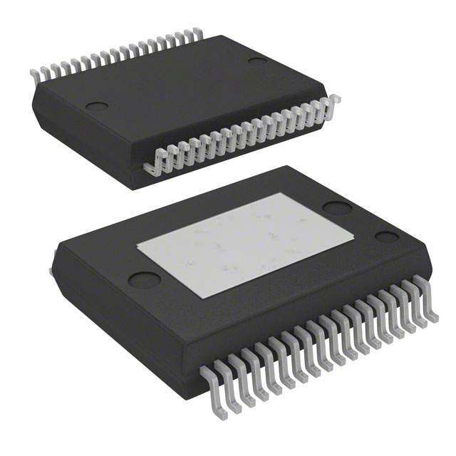
| 描述 | IC CTRLR SW SYNC STPDN 28TSSOP开关控制器 Two-Phase Sync SD Switching Cntlr |
| 产品分类 | |
| 品牌 | Texas Instruments |
| 产品手册 | |
| 产品图片 |
|
| rohs | 符合RoHS无铅 / 符合限制有害物质指令(RoHS)规范要求 |
| 产品系列 | 电源管理 IC,开关控制器 ,Texas Instruments LM2642MTC/NOPB- |
| 数据手册 | |
| 产品型号 | LM2642MTC/NOPB |
| 产品目录页面 | |
| 产品种类 | 开关控制器 |
| 供应商器件封装 | 28-TSSOP |
| 其它名称 | *LM2642MTC/NOPB |
| 包装 | 管件 |
| 占空比-最大 | 98 % |
| 商标 | Texas Instruments |
| 安装类型 | 表面贴装 |
| 安装风格 | SMD/SMT |
| 封装 | Tube |
| 封装/外壳 | 28-TSSOP(0.173",4.40mm 宽) |
| 封装/箱体 | TSSOP-28 |
| 工作温度 | -40°C ~ 125°C |
| 工厂包装数量 | 48 |
| 应用 | 嵌入式系统,控制台/机顶盒 |
| 开关频率 | 300 kHz |
| 最大工作温度 | + 125 C |
| 最小工作温度 | - 40 C |
| 标准包装 | 48 |
| 电压-电源 | 4.5 V ~ 30 V |
| 电流-电源 | 1mA |
| 系列 | LM2642 |
| 设计资源 | http://www.digikey.com/product-highlights/cn/zh/texas-instruments-webench-design-center/3176 |
| 输入电压 | 4.5 V to 30 V |
| 输出电压 | 1.3 V to 30 V |
| 输出电流 | 20 A |
| 输出端数量 | 2 Output |
| 配用 | /product-detail/zh/LM2642REVD%20EVAL/LM2642REVD%20EVAL-ND/1640600 |


- 商务部:美国ITC正式对集成电路等产品启动337调查
- 曝三星4nm工艺存在良率问题 高通将骁龙8 Gen1或转产台积电
- 太阳诱电将投资9.5亿元在常州建新厂生产MLCC 预计2023年完工
- 英特尔发布欧洲新工厂建设计划 深化IDM 2.0 战略
- 台积电先进制程称霸业界 有大客户加持明年业绩稳了
- 达到5530亿美元!SIA预计今年全球半导体销售额将创下新高
- 英特尔拟将自动驾驶子公司Mobileye上市 估值或超500亿美元
- 三星加码芯片和SET,合并消费电子和移动部门,撤换高东真等 CEO
- 三星电子宣布重大人事变动 还合并消费电子和移动部门
- 海关总署:前11个月进口集成电路产品价值2.52万亿元 增长14.8%


PDF Datasheet 数据手册内容提取
LM2642 www.ti.com SNVS203I–MAY2002–REVISEDAPRIL2013 LM2642 Two-Phase Synchronous Step-Down Switching Controller CheckforSamples:LM2642 FEATURES DESCRIPTION 1 • TwoSynchronousBuckRegulators The LM2642 consists of two current mode 2 synchronous buck regulator controllers with a • 180°OutofPhaseOperation switchingfrequencyof300kHz. • 4.5Vto30VInputRange The two switching regulator controllers operate 180° • PowerGoodFunctionMonitorsCh.1 out of phase. This feature reduces the input ripple • 37µAShutdownCurrent RMS current, thereby significantly reducing the • 0.04%(typical)LineandLoadRegulationError required input capacitance. The two switching regulator outputs can also be paralleled to operate as • CurrentModeControlWithorWithoutaSense adual-phasesingleoutputregulator. Resistor The output of each channel can be independently • IndependentEnable/Soft-startPinsAllow adjusted from 1.3 to V • maximum duty cycle. An SimpleSequentialStartupConfiguration. IN internal 5V rail is also available externally for driving • ConfigurableforSingleOutputParallel bootstrapcircuitry. Operation.(SeeFigure3). Current-mode feedback control assures excellent line • AdjustableCycle-by-CycleCurrentLimit and load regulation and a wide loop bandwidth for • InputUnder-voltageLockout excellent response to fast load transients. Current is sensed across either the Vds of the top FET or • OutputOver-voltageLatchProtection across an external current-sense resistor connected • OutputUnder-voltageProtectionwithDelay in series with the drain of the top FET. Current limit is • ThermalShutdown independentlyadjustableforeachchannel. • SelfDischargeofOutputCapacitorsWhenthe The LM2642 features analog soft-start circuitry that is RegulatorisOFF independent of the output load and output • TSSOPpackage capacitance. This makes the soft-start behavior more predictable and controllable than traditional soft-start APPLICATIONS circuits. • EmbeddedComputerSystems A PGOOD1 pin is provided to monitor the dc output of channel 1. Over-voltage protection is available for • HighEndGamingSystems both outputs. A UV-Delay pin is also available to • Set-topBoxes allow delayed shut off time for the IC during an output • WebPAD under-voltageevent. BLOCK DIAGRAM VIN 4.5V-30V H UV_Delay VOUT1 L 1.3V-27V PGOOD1 LM2642 SS/ON1 H SS/ON2 L 1.3VVOU-2T27V 1 Pleasebeawarethatanimportantnoticeconcerningavailability,standardwarranty,anduseincriticalapplicationsof TexasInstrumentssemiconductorproductsanddisclaimerstheretoappearsattheendofthisdatasheet. Alltrademarksarethepropertyoftheirrespectiveowners. 2 PRODUCTIONDATAinformationiscurrentasofpublicationdate. Copyright©2002–2013,TexasInstrumentsIncorporated Products conform to specifications per the terms of the Texas Instruments standard warranty. Production processing does not necessarilyincludetestingofallparameters.
LM2642 SNVS203I–MAY2002–REVISEDAPRIL2013 www.ti.com Thesedeviceshavelimitedbuilt-inESDprotection.Theleadsshouldbeshortedtogetherorthedeviceplacedinconductivefoam duringstorageorhandlingtopreventelectrostaticdamagetotheMOSgates. CONNECTION DIAGRAM TOPVIEW 1 28 KS1 RSNS1 2 27 ILIM1 SW1 3 26 COMP1 HDRV1 4 25 FB1 CBOOT1 5 24 PGOOD1 VDD1 6 23 UVDELAY LDRV1 7 22 VLIN5 VIN 8 21 SGND PGND 9 20 ON/SS1 LDRV2 10 19 ON/SS2 VDD2 11 18 FB2 CBOOT2 12 17 COMP2 HDRV2 13 16 ILIM2 SW2 14 15 KS2 RSNS2 Figure1. 28-LeadTSSOP PIN DESCRIPTIONS KS1(Pin1) Thepositive(+)KelvinsensefortheinternalcurrentsenseamplifierofChannel1.Useaseparate tracetoconnectthispintothecurrentsensepoint.ItshouldbeconnectedtoVINascloseaspossibleto thenodeofthecurrentsenseresistor.Whennocurrent-senseresistorisused,connectascloseas possibletothedrainnodeoftheupperMOSFET. ILIM1(Pin2) CurrentlimitthresholdsettingforChannel1.Itsinksaconstantcurrentof10µA,whichis convertedtoavoltageacrossaresistorconnectedfromthispintoVIN.Thevoltageacrosstheresistoris comparedwitheithertheVDSofthetopMOSFETorthevoltageacrosstheexternalcurrentsense resistortodetermineifanover-currentconditionhasoccurredinChannel1. COMP1(Pin3)CompensationpinforChannel1.Thisistheoutputoftheinternaltransconductanceamplifier. Thecompensationnetworkshouldbeconnectedbetweenthispinandthesignalground,SGND(Pin8). FB1(Pin4) Feedbackinputforchannel1.ConnecttoVOUTthroughavoltagedividertosetthechannel1 outputvoltage. PGOOD1(Pin5) Anopen-drainpower-goodoutputforChannel1.Itis'LOW'(lowimpedancetoground) whenevertheoutputvoltageofChannel1fallsoutsideofa+15%to-9%window.PGOOD1stayslatched ina'LOW'stateduringOVPorUVPoneitherchannel.Itwillrecovertoa'HIGH'state(highimpedanceto ground)afteraChannel1outputunder-voltageevent(<91%)whentheoutputreturnstowithin6%ofits nominalvalue.SeeOperationDescriptionsfordetails. UV_DELAY(Pin6) AcapacitorfromthispintogroundsetsthedelaytimeforUVP.Thecapacitorischarged froma5µAcurrentsource.WhenUV_DELAYchargesto2.3V(typical),thesystemimmediatelylatches off.Connectingthispintogroundwilldisabletheoutputunder-voltageprotection. VLIN5(Pin7)Theoutputofaninternal5VLDOregulatorderivedfromVIN.Itsuppliestheinternalbiasforthe chipandsuppliesthebootstrapcircuitryforgatedrive.Bypassthispintosignalgroundwithaminimumof 4.7µFcapacitor. SGND(Pin8)Thegroundconnectionforthesignal-levelcircuitry.Itshouldbeconnectedtothegroundrailofthe 2 SubmitDocumentationFeedback Copyright©2002–2013,TexasInstrumentsIncorporated ProductFolderLinks:LM2642
LM2642 www.ti.com SNVS203I–MAY2002–REVISEDAPRIL2013 system. ON/SS1(Pin9) Channel1enablepin.ThispinisinternallypulleduptoonediodedropaboveVLIN5.Pulling thispinbelow1.2V(open-collectortype)turnsoffChannel1.IfbothON/SS1andON/SS2pinsarepulled below1.2V,thewholechipgoesintoshutdownmode.Addingacapacitortothispinprovidesasoft-start featurethatminimizesinrushcurrentandoutputvoltageovershoot. ON/SS2(Pin10) Channel2enablepin.SeethedescriptionforPin9,ON/SS1.MaybeconnectedtoON/SS1for simultaneousstartuporforparalleloperation. FB2(Pin11)Feedbackinputforchannel2.ConnecttoVOUTthroughavoltagedividertosettheChannel2 outputvoltage. COMP2(Pin12) CompensationpinforChannel2.Thisistheoutputoftheinternaltransconductanceamplifier. ThecompensationnetworkshouldbeconnectedbetweenthispinandthesignalgroundSGND(Pin8). ILIM2(Pin13) CurrentlimitthresholdsettingforChannel2.SeeILIM1(Pin2). KS2(Pin14)Thepositive(+)KelvinsensefortheinternalcurrentsenseamplifierofChannel2.SeeKS1(Pin1). RSNS2(Pin15) Thenegative(-)KelvinsensefortheinternalcurrentsenseamplifierofChannel2.Connectthis pintothelowsideofthecurrentsenseresistorthatisplacedbetweenVINandthedrainofthetop MOSFET.WhentheRdsofthetopMOSFETisusedforcurrentsensing,connectthispintothesourceof thetopMOSFET.AlwaysuseaseparatetracetoformaKelvinconnectiontothispin. SW2(Pin16)Switch-nodeconnectionforChannel2,whichisconnectedtothesourceofthetopMOSFETof Channel2.Itservesasthenegativesupplyrailforthetop-sidegatedriver,HDRV2. HDRV2(Pin17)Top-sidegate-driveoutputforChannel2.HDRVisafloatingdriveoutputthatridesonthe correspondingswitching-nodevoltage. CBOOT2(Pin18) Bootstrapcapacitorconnection.ItservesasthepositivesupplyrailfortheChannel2top-side gatedrive.ConnectthispintoVDD2(Pin19)throughadiode,andconnectthelowsideofthebootstrap capacitortoSW2(Pin16). VDD2(Pin19) ThesupplyrailfortheChannel2low-sidegatedrive.ConnectedtoVLIN5(Pin7)througha4.7Ω resistorandbypassedtopowergroundwithaceramiccapacitorofatleast1µF.TiethispintoVDD1(Pin 24). LDRV2(Pin20) Low-sidegate-driveoutputforChannel2. PGND(Pin21) Thepowergroundconnectionforbothchannels.Connecttothegroundrailofthesystem. VIN(Pin22) Thepowerinputpinforthechip.Connecttothepositive(+)inputrailofthesystem.Thispinmust beconnectedtothesamevoltagerailasthetopFETdrain(orthecurrentsenseresistorwhenused). LDRV1(Pin23) Low-sidegate-driveoutputforChannel1. VDD1(Pin24)ThesupplyrailforChannel1low-sidegatedrive.TiethispintoVDD2(Pin19). CBOOT1(Pin25)Bootstrapcapacitorconnection.ItservesasthepositivesupplyrailforChannel1top-sidegate drive.SeeCBOOT2(Pin18). HDRV1(Pin26)Top-sidegate-driveoutputforChannel1.SeeHDRV2(Pin17). SW1(Pin27) Switch-nodeconnectionforChannel1.SeeSW2(Pin16). RSNS1(Pin28)Thenegative(-)KelvinsensefortheinternalcurrentsenseamplifierofChannel1.SeeRSNS2 (Pin15). Copyright©2002–2013,TexasInstrumentsIncorporated SubmitDocumentationFeedback 3 ProductFolderLinks:LM2642
LM2642 SNVS203I–MAY2002–REVISEDAPRIL2013 www.ti.com ABSOLUTE MAXIMUM RATINGS (1) VoltagesfromtheindicatedpinstoSGND/PGND: VIN,ILIM1,ILIM2,KS1,KS2 −0.3Vto32V SW1,SW2,RSNS1,RSNS2 −0.3to(V +0.3)V IN FB1,FB2,VDD1,VDD2 −0.3Vto6V PGOOD,COMP1,COMP2,UVDelay −0.3Vto(VLIN5+0.3)V ON/SS1,ON/SS2 (2) −0.3Vto(VLIN5+0.6)V CBOOT1toSW1,CBOOT2toSW2 −0.3Vto7V LDRV1,LDRV2 −0.3Vto(VDD+0.3)V HDRV1toSW1,HDRV2toSW2 −0.3V HDRV1toCBOOT1,HDRV2toCBOOT2 +0.3V PowerDissipation(T =25°C), A (3) 1.1W AmbientStorageTemperatureRange −65°Cto+150°C SolderingDwellTime,Temperature (4) Wave 4sec,260°C Infrared 10sec,240°C VaporPhase 75sec,219°C ESDRating (5) 2kV (1) Absolutemaximumratingsindicatelimitsbeyondwhichdamagetothedevicemayoccur.OperatingRangeindicatesconditionsfor whichthedeviceisintendedtobefunctional,butdoesnotensurespecificperformancelimits.Forensuredspecificationsandtest conditions,seetheElectricalCharacteristics.Thespecificationsapplyonlyforthetestconditions.Someperformancecharacteristics maydegradewhenthedeviceisnotoperatedunderthelistedtestconditions. (2) ON/SS1andON/SS2areinternallypulleduptoonediodedropaboveVLIN5.Donotapplyanexternalpull-upvoltagetothesepins.It maycausedamagetotheIC. (3) ThemaximumallowablepowerdissipationiscalculatedbyusingP =(T -T )/θ ,whereT isthemaximumjunction DMAX JMAX A JA JMAX temperature,T istheambienttemperatureandθ isthejunction-to-ambientthermalresistanceofthespecifiedpackage.The1.1W A JA ratingresultsfromusing125°C,25°C,and90.6°C/WforT ,T ,andθ respectively.Aθ of90.6°C/Wrepresentstheworst-case JMAX A JA JA conditionofnoheatsinkingofthe28-pinTSSOP.Athermalshutdownwilloccurifthetemperatureexceedsthemaximumjunction temperatureofthedevice. (4) Fordetailedinformationonsolderingplasticsmall-outlinepackages,seetheTIwebsiteatwww.ti.com/packaging. (5) Fortestingpurposes,ESDwasappliedusingthehuman-bodymodel,a100pFcapacitordischargedthrougha1.5kΩresistor. OPERATING RATINGS (1) VIN(VLIN5tiedtoVIN) 4.5Vto5.5V VIN(VINandVLIN5separate) 5.5Vto30V JunctionTemperature −40°Cto+125°C (1) Absolutemaximumratingsindicatelimitsbeyondwhichdamagetothedevicemayoccur.OperatingRangeindicatesconditionsfor whichthedeviceisintendedtobefunctional,butdoesnotensurespecificperformancelimits.Forensuredspecificationsandtest conditions,seetheElectricalCharacteristics.Thespecificationsapplyonlyforthetestconditions.Someperformancecharacteristics maydegradewhenthedeviceisnotoperatedunderthelistedtestconditions. 4 SubmitDocumentationFeedback Copyright©2002–2013,TexasInstrumentsIncorporated ProductFolderLinks:LM2642
LM2642 www.ti.com SNVS203I–MAY2002–REVISEDAPRIL2013 ELECTRICAL CHARACTERISTICS Unlessotherwisespecified,V =15V,GND=PGND=0V,VLIN5=VDD1=VDD2.Limitsappearinginboldfacetypeapply IN overthespecifiedoperatingjunctiontemperaturerange,(-20°Cto+125°C,ifnototherwisespecified).Specifications appearinginplaintypearemeasuredusinglowdutycyclepulsetestingwithT =25°C (1), (2).Min/Maxlimitsarespecifiedby A design,test,orstatisticalanalysis. Symbol Parameter Conditions Min Typ Max Units System ΔV /V LoadRegulation VIN=15V,V =0.5Vto1.5V 0.04 % OUT OUT compx ΔV /V LineRegulation 5.5V≤VIN≤30V,V =1.25V 0.04 % OUT OUT compx V FeedbackVoltage 5.5V≤VIN≤30V 1.215 1.238 1.260 FB1_FI2 0°Cto125°C 1.217 1.259 V -40°Cto125°C 1.212 1.261 I InputSupplyCurrent V >2V 1.0 VIN ON_SSx mA 5.5V≤VIN≤30V 2.0 Shutdown (3) 37 µA V =V =0V 110 ON_SS1 ON_SS2 VLIN5 VLIN5OutputVoltage (4) IVLIN5=0to25mA, 4.70 5 5.30 5.5V≤VIN≤30V V -40°Cto125°C 4.68 5.30 V CurrentLimitComparator CLos ±2 ±7.0 mV Offset(VILIMX−VRSNSX) I CurrentLimitSinkCurrent 9 10 11 CL µA -40°Cto125°C 8.67 11 I , Soft-StartSourceCurrent V =V =1.5V(on) ss_SC1 ON_ss1 ON_ss2 0.5 2 5.0 µA I ss_SC2 I , Soft-StartSinkCurrent V =V =2V ss_SK1 ON_ss1 ON_ss2 2 5.2 10 µA I ss_SK2 V , Soft-StartOnThreshold ON_SS1 0.7 1.12 1.4 V V ON_SS2 V Soft-StartTimeout (5) SSTO 3.3 V Threshold I UV_DELAYSourceCurrent UV-DELAY=2V 2 5 9 µA sc_uvdelay I UV_DELAYSinkCurrent UV-DELAY=0.4V 0.2 0.48 1.2 mA sk_uvdelay V UV_DELAYThreshold UVDelay 2.3 V Voltage V FB1,FB2,UnderVoltage Asapercentageofnominaloutputvoltage UVP 75 80 86 % ProtectionLatchThreshold (fallingedge) Hysteresis 4 % V V Overvoltage AsapercentagemeasuredatV ,V OVP OUT FB1 FB2 107 113 122 % ShutdownLatchThreshold V RegulatorWindowDetector Asapercentageofoutputvoltage pwrbad Thresholds(PGOOD1from 86.5 90.3 94.5 % HightoLow) V RegulatorWindowDetector pwrgd Thresholds(PGOOD1from 91.5 94 97.0 % LowtoHigh) S SW1,SW2ON-Resistance V =V =2V 420 480 535 Ω wx_R SW1 SW2 GateDrive I CBOOTxLeakageCurrent V =V =7V 10 nA CBOOT CBOOT1 CBOOT2 (1) AtypicalisthecenterofcharacterizationdatameasuredwithlowdutycyclepulsetstingatT =25°C.Typicalsarenotensured. A (2) Alllimitsarespecified.Allelectricalcharacteristicshavingroom-temperaturelimitsaretestedduringproductionwithT =T =25°C.All A J hotandcoldlimitsarespecifiedbycorrelatingtheelectricalcharacteristicstoprocessandtemperaturevariationsandapplyingstatistical processcontrol. (3) Bothswitchingcontrollersareoff.ThelinearregulatorVLIN5remainson. (4) TheoutputvoltageattheVLIN5pinmaybeashighas5.9Vinshutdownmode(ON/SS1=ON/SS2=0V). (5) WhenSS1andSS2pinsarechargedabovethisvoltageandeitheroftheoutputvoltagesatVout1orVout2isstillbelowtheregulation limit,theundervoltageprotectionfeatureisinitialized. Copyright©2002–2013,TexasInstrumentsIncorporated SubmitDocumentationFeedback 5 ProductFolderLinks:LM2642
LM2642 SNVS203I–MAY2002–REVISEDAPRIL2013 www.ti.com ELECTRICAL CHARACTERISTICS (continued) Unlessotherwisespecified,V =15V,GND=PGND=0V,VLIN5=VDD1=VDD2.Limitsappearinginboldfacetypeapply IN overthespecifiedoperatingjunctiontemperaturerange,(-20°Cto+125°C,ifnototherwisespecified).Specifications appearinginplaintypearemeasuredusinglowdutycyclepulsetestingwithT =25°C(1),(2).Min/Maxlimitsarespecifiedby A design,test,orstatisticalanalysis. Symbol Parameter Conditions Min Typ Max Units I HDRVxandLDRVxSource V =V =5V,VSWx=0V, SC_DRV CBOOT1 CBOOT2 0.5 A Current HDRVx=LDRVx=2.5V I HDRVxSinkCurrent V =VDDx=5V,V =0V,HDRVX sk_HDRV CBOOTx SWx 0.8 A =2.5V I LDRVxSinkCurrent V =VDDx=5V,V =0V,LDRVX sk_LDRV CBOOTx SWx 1.1 A =2.5V R HDRV1&2SourceOn- V =V =5V, HDRV CBOOT1 CBOOT2 3.1 Ω Resistance V =V =0V SW1 SW2 HDRV1&2SinkOn- 1.5 Ω Resistance R LDRV1&2SourceOn- V =V =5V, LDRV CBOOT1 CBOOT2 3.1 Ω Resistance V =V =0V SW1 SW2 V =V =5V LDRV1&2SinkOn- DD1 DD1 1.1 Ω Resistance Oscillator F OscillatorFrequency 260 300 340 osc kHz -40°Cto125°C 257.5 340 Don_max MaximumOn-DutyCycle V =V =1V,Measuredatpins FB1 FB2 96 98 HDRV1andHDRV2 % -40°Cto125°C 95.64 T MinimumOn-Time 166 ns on_min SS HDRV1andHDRV2Delta ON/SS1=ON/SS2=2V OT_delta 20 150 ns OnTime ErrorAmplifier I ,I FeedbackInputBias V =1.5V,V =1.5V FB1 FB2 FB1_FIX FB2_FIX 65 ±200 nA Current I , COMPOutputSource V =V =1V, comp1_SC FB1_FIX FB2_FIX 18 113 I Current V =V =1V comp2_SC COMP1 COMP2 µA 0°Cto125°C 32 -40°Cto125°C 6 I , COMPOutputSinkCurrent V =V =1.5Vand comp1_SK FB1_FIX FB2_FIX 18 108 I V =V =0.5V comp2_SK COMP1 COMP2 µA 0°Cto125°C 32 -40°Cto125°C 6 gm1,gm2 Transconductance 650 µmho GI , CurrentSenseAmplifier V =1.25V SNS1 COMPx 4.2 5.2 7.5 GI (1&2)Gain SNS2 VoltageReferencesandLinearVoltageRegulators UVLO VLIN5Under-voltage ON/SS1,ON/SS2transition Lockout fromlowtohigh 3.6 4.0 4.4 V ThresholdRising LogicOutputs I PGOODLowSinkCurrent V =0.4V 0.60 0.95 mA OL PGOOD I PGOODHighLeakage V =5V OH PGOOD 5 200 nA Current 6 SubmitDocumentationFeedback Copyright©2002–2013,TexasInstrumentsIncorporated ProductFolderLinks:LM2642
LM2642 www.ti.com SNVS203I–MAY2002–REVISEDAPRIL2013 VIN+6V-30V C2 10nF GND 22 2 R1 VIN ILIM1 1Cu1F LMIC26142 KS1 1 13k 28 +C6 RSNS1 C5 22uF 10uF Q1 6 26 UV_DELAY HDRV1 FDS6690A Vo1 0C.314uF SW1 27 R32 L1 5V/3A C7 4R7 VDD 8.2uH VLIN25R2208k CBOOT1 250.1uF BADW3A56 +1C080uF R601k04 PGOOD1 5 PGOOD1 LDRV1 23 D4 R11 Q2 MBRS140T3 20k 21 FDS6690A PGND 9 ON/SS1 4 C11 FB1 10nF 11 FB2 C13 10nF 10 ON/SS2 13 R13 C12 ILIM2 VIN 10nF 24 14 13k VDD1 KS2 +C16 VDD 19 15 22uF VDD2 RSNS2 C17 R27 VLIN5 7 VLIN5 Q3 10uF 17 4R7 C4.276uF 3 COMP1 HDRV2 16 R33 FDS6690A L2 3.3VVo/23A SW2 C1u2F7 R23 1Cn1F9 1Cn2F0 12 COMP2 CBOOT2 180.C12u5F D43RB7 VDD 6uH10C0u2F2 + R331k92 20k R24 BAW56 20k 8 SGND LDRV2 20 D5 MBRS140T3 R20 Q4 20k FDS6690A Figure2. Typical2ChannelApplicationCircuit Copyright©2002–2013,TexasInstrumentsIncorporated SubmitDocumentationFeedback 7 ProductFolderLinks:LM2642
LM2642 SNVS203I–MAY2002–REVISEDAPRIL2013 www.ti.com VIN+ 4.5V-20V C1 1uF C210nF C3 100pF GND R1 R2 VIN ILIM1 11k 100R C5 C6 KS1 R7 10uF 22uF 12m C4 R6 RSNS1 100pF 100R C34 UV_DELAY HDRV1 Q1 Vout VLIN5 0.1uF R32 L1 1.8V/14A SW1 3u6H + + 4R7 C8 C9 R28 CBOOT1 VDD 220uF 220uF 220K PGOOD1 PGOOD1 Q2 C7 R9k10 GND LDRV1 0.1uF D3A R11 ON1/2 ON/SS1 D4 20k PGND C11 22nF S1 ON/SS2 FB1 IC1 C13 10nF C14100pF LM2642 VIN R13 R14 ILIM2 11K 100R C17 C16 KS2 R15 10uF 22uF 12m C15 R16 RSNS2 COMP1 100R 100pF COMP2 C19 HDRV2 Q3 L2 2.2nF R33 C18 VLIN5 SW2 470pF 4R7 3u6H R23 + + 20k VDD1 CBOOT2 VDD 2C202u2F C22203uF R27 VDD2 C25 4R7 C26 C27 LDRV2 Q4 0.1uF D3B D5 4.7uF 1uF SGND FB2 Figure3. TypicalSingleChannelApplicationCircuit 8 SubmitDocumentationFeedback Copyright©2002–2013,TexasInstrumentsIncorporated ProductFolderLinks:LM2642
LM2642 www.ti.com SNVS203I–MAY2002–REVISEDAPRIL2013 BLOCK DIAGRAM VIN Input Power Supply Voltage and SD Disable BG BG gCenuerrreantotr GenBeiarastor +- reference IREF Cubriraesnt Vref +- (5AVll wLDayOs ON) VLIN5 From another Ch. 10uA COMPx Ch1 and Ch2 are identical CoImLIpM ILIMx + - KSx CHx + output - RSNSx ISENSE amp FBx erro-r amp ONNormal: +- PWM comp &S hlaifttcehr CBOOTx + PWM logic control R Q HDRVx BG SS: S Q ON Corrective SWx COHutxput 2uA ON/OF&F ramp - Shoot through + S/S + protection ON/SSx control S/S level 0.50V +- CcSoykmciplpe sequencer VDDx LDRVx 7uA PGNDx FAULT fault TSD UVLO Active discharge Rdson= 5uA UVP 500 Ohm R Q UV_DELAY S Q UV UVP OVP To Ch2 R Q coUmVpParGa1tor Fanroomther 0 180 S Q CH. OSC Reset by 300 kHz POR or SD OVP PGOOD SGND Copyright©2002–2013,TexasInstrumentsIncorporated SubmitDocumentationFeedback 9 ProductFolderLinks:LM2642
LM2642 SNVS203I–MAY2002–REVISEDAPRIL2013 www.ti.com TYPICAL PERFORMANCE CHARACTERISTICS SoftstartWaveforms PowerOnandPGOOD1Waveforms (I =I =0A) (I =I =0A) LOAD1 LOAD2 LOAD1 LOAD2 VOUT1 2V/div PGOOD1 5V/div VIN VOUT2 22V/div 2V/div VOUT1 2V/div VOUT1 ON/SS1=ON/SS2 2V/div 2V/div VIN VOUT2 ON/SS1=ON/SS2 7V/div 2V/div 1V/div VIN 10V/div 2ms/div 2ms/div Figure4. Figure5. Over-CurrentandUVPShutdown UVPStartupWaveforms (I =0A) LOAD2 ILOAD 10A/div ILOAD 10A/div VOUT1 VOUT 2V/div 1V/div VOUT2 1V/div ON/SS 2V/div UV_DELAY 2V/div UV_DELAY 10ms/div 10ms/div Figure6. Figure7. ShutdownWaveforms Ch.1LoadTransientResponse (I =I =0A) 5V ,12V LOAD1 LOAD2 OUT IN VOUT1 2V/div VOUT2 2V/div ON/SS1=ON/SS2 5V/div 100ms/div Figure8. Figure9. 10 SubmitDocumentationFeedback Copyright©2002–2013,TexasInstrumentsIncorporated ProductFolderLinks:LM2642
LM2642 www.ti.com SNVS203I–MAY2002–REVISEDAPRIL2013 Ch.2LoadTransientResponse LoadTransientResponse 3.3V ,12V ParallelOperation1.8V ,12V OUT IN OUT IN Figure10. Figure11. InputSupplyCurrent InputSupplyCurrent vs vs Temperature V IN (ShutdownModeV =15V) ShutdownMode(25°C) IN 44 49 42 47 45 40 Iq (A)P 38 Iq (uA) 4431 36 39 34 37 32 35 -25 -5 15 35 55 75 95 115 135 5.5 10.5 15.5 20.5 25.5 30 VIN (V) TEMPERATURE (oC) Figure12. Figure13. VLIN5 VLIN5 vs vs Temperature V (25°C) IN 5.07 5.06 5.05 5.06 VIN=30V 5.04 5.05 5.03 V) V) N5 ( 5.04 VIN=5.5V N5 ( 5.02 VLI VLI 5.01 5.03 5 5.02 4.99 5.01 4.98 -25 -5 15 35 55 75 95 115 135 5.5 10.5 15.5 20.5 25.5 30 TEMPERATURE (oC) VIN (V) Figure14. Figure15. Copyright©2002–2013,TexasInstrumentsIncorporated SubmitDocumentationFeedback 11 ProductFolderLinks:LM2642
LM2642 SNVS203I–MAY2002–REVISEDAPRIL2013 www.ti.com FBReferenceVoltage OperatingFrequency vs vs Temperature Temperature 1.244 320 315 1.242 310 1.240 Hz) 305 k V (V)REF 1.238 QUENCY ( 322099050 1.236 E R F 285 1.234 280 275 1.232 270 -40 -20 0 20 40 60 80 100 120 -40 -20 0 20 40 60 80 100 120 TEMPERATURE (oC) TEMPERATURE (oC) Figure16. Figure17. Efficiency ErrorAmplifierGain vs vs LoadCurrent Temperature Ch.1=5V,Ch.2=Off 700.0 100 650.0 90 VIN=7V mho) 600.0 Y (%) 80 VIN=22V m (u 550.0 ENC 70 g CI EA 500.0 EFFI 60 VIN=12V 450.0 50 400.0 40 -40 -20 0 20 40 60 80 100 120140 1.E-02 1.E-01 1.E+00 1.E+01 JUNCTION TEMPEARTURE (oC) LOAD CURRENT(A) Figure18. Figure19. Efficiency Efficiency vs vs LoadCurrent LoadCurrent Ch.2=2.5V,Ch.1=Off Ch.2=3.3V,Ch.1=Off 100 100 90 VIN=7V 90 VIN=7V CIENCY (%) 8700 VIN=22V ENCY (%) 8700 VIN=22V FI CI EF 60 VIN=12V EFFI 60 VIN=12V 50 50 40 40 1.E-02 1.E-01 1.E+00 1.E+01 1.E-02 1.E-01 1.E+00 1.E+01 LOAD CURRENT(A) LOAD CURRENT(A) Figure20. Figure21. 12 SubmitDocumentationFeedback Copyright©2002–2013,TexasInstrumentsIncorporated ProductFolderLinks:LM2642
LM2642 www.ti.com SNVS203I–MAY2002–REVISEDAPRIL2013 APPLICATION INFORMATION OPERATION DESCRIPTIONS SOFTSTART The ON/SS1 pin has dual functionality as both channel enable and soft start control. The soft start block diagram isshowninFigure22. The LM2642 will remain in shutdown mode while both soft start pins are grounded.In a normal application (with a soft start capacitor connected between the ON/SS1 pin and SGND) soft start functions as follows. As the input voltage rises (note: Iss starts to flow when VIN ≥ 2.2V), the internal 5V LDO starts up, and an internal 2µA current charges the soft start capacitor. During soft start phase, the error amplifier output voltage at the COMPx pin is clamped at 0.55V and the duty cycle is controlled only by the soft start voltage. As the SSx pin voltage rampsup,thedutycycleincreasesproportionaltothesoftstartramp,causingtheoutputvoltagetorampup.The rate at which the duty cycle increases depends on the capacitance of the soft start capacitor. The higher the capacitance, the slower the output voltage ramps up. When the corresponding output voltage exceeds 98% (typical) of the set target voltage, the regulator switches from soft start to normal operating mode. At this time, the 0.55V clamp at the output of the error amplifier releases and peak current feedback control takes over. Once in peak current feedback control mode, the output of the error amplifier will travel within the 0.5V and 2V window toachievePWMcontrol.SeeFigure23. Duringsoftstart,over-voltageprotectionandcurrentlimitremainineffect.Theundervoltageprotectionfeatureis activated when the ON/SS pin exceeds the timeout threshold (3.3V typical). If the ON/SSx capacitor is too small, thedutycyclemayincreasetoorapidly,causingthedevicetolatchoffduetooutputvoltageovershootabovethe OVPthreshold.Thisbecomesmorelikelyinapplicationsrequiringlowoutputvoltage,highinputvoltageandlight load.Acapacitanceof10nFisrecommendedateachsoftstartpintoprovideasmoothmonotonicoutputramp. + R Q - S>R 2uA disable S Q fault ONx ON/SSx + - 1.2V/ ON/OFF ON: 2uA source 1.05V comparator 7uA Fault: 5uA sink + S/S level - S/S buffer Figure22. SoftStartandON/OFF low clamp + - 0.45V COMPx + - SS:0.55V high clamp OP:2V Figure23. VoltageClampatCOMPxPin Copyright©2002–2013,TexasInstrumentsIncorporated SubmitDocumentationFeedback 13 ProductFolderLinks:LM2642
LM2642 SNVS203I–MAY2002–REVISEDAPRIL2013 www.ti.com SEQUENTIALSTARTUP Sequential startup can be implemented by simply connecting PGOOD1 to SS/ON2. Once channel 1 has reached 94% of nominal, PGOOD1 will go high, thus enabling SS/ON2. In this mode of operation, channel 2 will be controlled by the state of channel 1. If channel 1 falls out of the PGOOD1 window, channel 2 will be switched off immediately. PGOOD1 OFF 1 UVPG1 UVP½ (latched) FBx OVP½ (latched) shutdown from other CH. latch OVP HDRV: off LDRV: on OVP1/2 OVP& PG 1.13BG _ OVPx + _ UVPG UVPGx in: 0.94BG + out: 0.91BG 5 µA _ UVP UVPx UV_DELAY in: 0.84BG + ONx out: 0.80BG SSTimeout PGOOD Protection from other CH. Comparators SD power on reset shutdown latch UVP HDRV: off fault LDRV: off TSD UVLO Figure24. PGOOD,OVPandUVP OVERVOLTAGEPROTECTION(OVP) If the output voltage on either channel rises above 113% of nominal, over voltage protection activates. Both channels will latch off, and the PGOOD1 pin will go low. When the OVP latch is set, the high side FET driver, HDRVx, is immediately turned off and the low side FET driver, LDRVx, is turned on to discharge the output capacitor through the inductor. To reset the OVP latch, either the input voltage must be cycled, or both channels mustbeswitchedoff. UNDERVOLTAGEPROTECTION(UVP)ANDUVDELAY If the output voltage on either channel falls below 80% of nominal, under voltage protection activates. As shown in Figure 24, an under-voltage event will shut off the UV_DELAY MOSFET, which will allow the UV_DELAY capacitor to charge at 5uA (typical). At the UV_DELAY threshold (2.3V typical) both channels will latch off. Also, UV_DELAY will be disabled and the UV_DELAY pin will return to 0V. During UVP, both the high side and low side FET drivers will be turned off. If no capacitor is connected to the UV_DELAY pin, the UVP latch will be activated immediately. To reset the UVP latch, either the input voltage must be cycled, or both ON/SS pins must bepulledlow.TheUVPfunctioncanbedisabledbyconnectingtheUV_DELAYpintoground. 14 SubmitDocumentationFeedback Copyright©2002–2013,TexasInstrumentsIncorporated ProductFolderLinks:LM2642
LM2642 www.ti.com SNVS203I–MAY2002–REVISEDAPRIL2013 POWERGOOD A power good pin (PGOOD1) is available to monitor the output status of Channel 1. As shown in Figure 24, the pin connects to the output of an open drain MOSFET, which will remain open while Channel 1 is within operating range.PGOOD1willgolow(lowimpedancetoground)underthefollowingfourconditions: 1. Channel1isturnedoff 2. Channel1outputfallsbelow90.3%ofnominal(UVPG1) 3. OVPoneitherchannel 4. UVPoneitherchannel When on, the PGOOD1 pin is capable of sinking 0.95mA (typical). If an OVP or UVP condition occurs, both channels will latch off, and the PGOOD1 pin will be latched low. During a UVPG1 condition, however, PGOOD1 will not latch off. The pin will stay low until Channel 1 output voltage returns to 94% (typical) of nominal. See VpwrgdintheElectricalCharacteristicstable. OUTPUTCAPACITORDISCHARGE Each channel has an embedded 480Ω MOSFET with the drain connected to the SWx pin. This MOSFET will discharge the output capacitor of its channel if its channel is off, or the IC enters a fault state caused by one of thefollowingconditions: 1. UVP 2. UVLO 3. Thermalshut-down(TSD) If an output over voltage event occurs, the HDRVx will be turned off and LDRVx will be turned on immediately to dischargetheoutputcapacitorofbothchannelsthroughtheinductor. BOOTSTRAPDIODESELECTION The bootstrap diode and capacitor form a supply that floats above the switch node voltage. VLIN5 powers this supply, creating approximately 5V (minus the diode drop) which is used to power the high side FET drivers and driver logic. When selecting a bootstrap diode, Schottky diodes are preferred due to their low forward voltage drop, but care must be taken for circuits that operate at high ambient temperature. The reverse leakage of some Schottky diodes can increase by more than 1000x at high temperature, and this leakage path can deplete the charge on the bootstrap capacitor, starving the driver and logic. Standard PN junction diodes and fast rectifier diodes can also be used, and these types maintain tighter control over reverse leakage current across temperature. SWITCHINGNOISEREDUCTION Power MOSFETs are very fast switching devices. In synchronous rectifier converters, the rapid increase of drain current in the top FET coupled with parasitic inductance will generate unwanted Ldi/dt noise spikes at the source node of the FET (SWx node) and also at the VIN node. The magnitude of this noise will increase as the output current increases. This parasitic spike noise may turn into electromagnetic interference (EMI), and can also causeproblemsindeviceperformance.Therefore,itmustbesuppressedusingoneofthefollowingmethods. It is strongly recommended to add R-C filters to the current sense amplifier inputs as shown in Figure 26. This will reduce the susceptibility to switching noise, especially during heavy load transients and short on time conditions. The filter components should be connected as close as possible to the IC. Note that these filters shouldbeusedwhenacurrentsenseresistorisused. As shown in Figure 25, adding a resistor in series with the SWx pin will slow down the gate drive (HDRVx), thus slowingtheriseandfalltimeofthetopFET,yieldingalongerdraincurrenttransitiontime. Usually a 3.3Ω to 4.7Ω resistor is sufficient to suppress the noise. Top FET switching losses will increase with higherresistancevalues. Small resistors (1-5 ohms) can also be placed in series with the HDRVx pin or the CBOOTx pin to effectively reduce switch node ringing. A CBOOT resistor will slow the rise time of the FET, whereas a resistor at HDRV will reducebothriseandfalltimes. Copyright©2002–2013,TexasInstrumentsIncorporated SubmitDocumentationFeedback 15 ProductFolderLinks:LM2642
LM2642 SNVS203I–MAY2002–REVISEDAPRIL2013 www.ti.com CBOOTx HDRVx 0.1uF SWx 4R7 Rsw Figure25. SWSeriesResistor CURRENTSENSINGANDLIMITING As shown in Figure 26, the KSx and RSNSx pins are the inputs of the current sense amplifier. Current sensing is accomplished either by sensing the Vds of the top FET or by sensing the voltage across a current sense resistor connected from VIN to the drain of the top FET. The advantage of sensing current across the top FET are reduced parts count, cost and power loss, whereas using a current sense resistor improves the current sense accuracy. Keeping the differential current-sense voltage below 200mV ensures linear operation of the current sense amplifier. Therefore, the Rdson of the top FET or the current sense resistor must be small enough so that the current sense voltage does not exceed 200mV when the top FET is on. There is a leading edge blanking circuit that forces the top FET on for at least 166ns. Beyond this minimum on time, the output of the PWM comparator is used to turn off the top FET. Additionally, a minimum voltage of at least 50mV across Rsns is recommendedtoensureahighSNRatthecurrentsenseamplifier. Assumingamaximumof200mVacrossRsns,thecurrentsenseresistorcanbecalculatedasfollows: (1) where Imax is the maximum expected load current, including overload multiplier (ie:120%), and Irip is the inductor ripple current (See equation 7). The above equation gives the maximum allowable value for Rsns. SwitchinglosseswillincreasewithRsns,thusloweringefficiency. The peak current limit is set by an external resistor connected between the ILIMx pin and the KSx pin. An internal 10µA current sink on the ILIMx pin produces a voltage across the resistor to set the current limit threshold which is compared to the current sense voltage. A 10nF capacitor across this resistor is required to filterunwantednoisethatcouldimproperlytripthecurrentlimitcomparator. 10uA LIMx comp LIMx 13k + POWER - SUPPLY KSx 10nF 100 + - ISEN SE RSNSx 100 20m amp 100pF 100pF Figure26. CurrentSenseandCurrentLimit Current limit is activated when the inductor current is high enough to cause the voltage at the RSNSx pin to be lower than that of the ILIMx pin. This toggles the comparator, thus turning off the top FET immediately. The comparator is disabled either when the top FET is turned off or during the leading edge blanking time. The equationforcurrentlimitresistor,R ,isasfollows: lim 16 SubmitDocumentationFeedback Copyright©2002–2013,TexasInstrumentsIncorporated ProductFolderLinks:LM2642
LM2642 www.ti.com SNVS203I–MAY2002–REVISEDAPRIL2013 (2) WhereIlimistheloadcurrentatwhichthecurrentlimitcomparatorwillbetripped. When sensing current across the top FET, replace Rsns with the Rdson of the FET. This calculated Rlim value specifiesthattheminimumcurrentlimitwillnotbelessthanImax.Itisrecommendedthata1%toleranceresistor beused. When sensing across the top FET, Rdson will show more variation than a current sense resistor, largely due to temperature. Rdson will increase proportional to temperature according to a specific temperature coefficient. Refertothemanufacturer'sdatasheettodeterminetherangeofRdsonvaluesoveroperatingtemperatureorsee the Component Selection section (equation 12) for a calculation of maximum Rdson. This will prevent Rdson variationsfromprematurelysettingoffthecurrentlimitcomparatorastheoperatingtemperatureincreases. To ensure accurate current sensing, special attention in board layout is required. The KSx and RSNSx pins requireseparatetracestoformaKelvinconnectiontothecorrespondingcurrentsensenodes. INPUTUNDERVOLTAGELOCKOUT(UVLO) The input under-voltage lock out threshold, which is sensed via the VLIN5 internal LDO output, is 4.0V (typical). Below this threshold, both HDRVx and LDRVx will be turned off and the internal 480Ω MOSFETs will be turned on to discharge the output capacitors through the SWx pins. During UVLO, the ON/SS pins will sink 5mA to discharge the soft start capacitors and turn off both channels. As the input voltage increases again above 4.0V, UVLO will be de-activated, and the device will restart again from soft start phase. If the voltage at VLIN5 remains below4.5V,butabovethe4.0VUVLOthreshold,thedevicecannotbeensuredtooperatewithinspecification. If the input voltage is between 4.0V and 5.2V, the VLIN5 pin will not regulate, but will follow approximately 200mVbelowtheinputvoltage. DUAL-PHASEPARALLELOPERATION In applications with high output current demand, the two switching channels can be configured to operate as a two-180° out of phase converter to provide a single output voltage with current sharing between the two switching channels. This approach greatly reduces the stress and heat on the output stage components while lowering input ripple current. The sum of inductor ripple current is also reduced which results in lowering output ripple voltage. Figure 3 shows an example of a typical two-phase circuit. Because precision current sense is the primary design criteria to ensure accurate current sharing between the two channels, both channels must use external sense resistors for current sensing. To minimize the error between the error amplifiers of the two channels, tie the feedback pins FB1 and FB2 together and connect to a single voltage divider for output voltage sensing. Also, tie the COMP1 and COMP2 together and connect to the compensation network. ON/SS1 and ON/SS2mustbetiedtogethertoenableanddisablebothchannelssimultaneously. COMPONENT SELECTION OUTPUTVOLTAGESETTING The output voltage for each channel is set by the ratio of a voltage divider as shown in Figure 27. The resistor valuescanbedeterminedbythefollowingequation: (3) Where Vfb=1.238V. Although increasing the value of R1 and R2 will increase efficiency, this will also decrease accuracy. Therefore, a maximum value is recommended for R2 in order to keep the output within .3% of Vnom. ThismaximumR2valueshouldbecalculatedfirstwiththefollowingequation: (4) Where200nAisthemaximumcurrentdrawnbyFBxpin. Copyright©2002–2013,TexasInstrumentsIncorporated SubmitDocumentationFeedback 17 ProductFolderLinks:LM2642
LM2642 SNVS203I–MAY2002–REVISEDAPRIL2013 www.ti.com Vout R2 FBx GND R1 Figure27. OutputVoltageSetting Example:Vnom=5V,Vfb=1.238V,Ifbmax=200nA. (5) Choose60K (6) The output voltage is limited by the maximum duty cycle as well as the minimum on time. Figure 28 shows the limits for input and output voltages. The recommended maximum output voltage is approximately 1V less than the nominal input voltage. At 30V input, the minimum output is approximately 2.3V and the maximum is approximately27V. For input voltages below 5.5V, VLIN5 must be connected to Vin through a small resistor (approximately 4.7 ohm).ThiswillensurethatVLIN5doesnotfallbelowtheUVLOthreshold. 30 25 20 UT VO 15 10 5 0 0 2 4 6 8 1012141618202224262830 VIN Figure28. AvailableOutputVoltageRange OUTPUT CAPACITOR SELECTION In applications that exhibit large and fast load current swings, the slew rate of such a load current transient may be beyond the response speed of the regulator. Therefore, to meet voltage transient requirements during worst- case load transients, special consideration should be given to output capacitor selection. The total combined ESR of the output capacitors must be lower than a certain value, while the total capacitance must be greater than a certain value. Also, in applications where the specification of output voltage regulation is tight and ripple voltagemustbelow,startingfromtherequiredoutputvoltageripplewilloftenresultinfewerdesigniterations. ALLOWEDTRANSIENTVOLTAGEEXCURSION Theallowedoutputvoltageexcursionduringaloadtransient(ΔVc_s)is: (7) 18 SubmitDocumentationFeedback Copyright©2002–2013,TexasInstrumentsIncorporated ProductFolderLinks:LM2642
LM2642 www.ti.com SNVS203I–MAY2002–REVISEDAPRIL2013 Where±δ%istheoutputvoltageregulationwindowand±ε%istheoutputvoltageinitialaccuracy. Example:Vnom=5V,δ%=7%,ε%=3.4%,Vrip=40mVpeaktopeak. (8) Since the ripple voltage is included in the calculation of ΔVc_s, the inductor ripple current should not be included in the worst-case load current excursion. That is, the worst-case load current excursion should be simply maximumloadcurrentchangespecification,ΔIc_s. MAXIMUMESRCALCULATION Unless the rise and fall times of a load transient are slower than the response speed of the control loop, if the total combined ESR (Re) is too high, the load transient requirement will not be met, no matter how large the capacitance. ThemaximumallowedtotalcombinedESRis: (9) Example:ΔVc_s=160mV,ΔIc_s=3A.ThenRe_max=53.3mΩ. Maximum ESR criterion can be used when the associated capacitance is high enough, otherwise more capacitorsthanthenumberdeterminedbythiscriterionshouldbeusedinparallel. MINIMUMCAPACITANCECALCULATION In a switch mode power supply, the minimum output capacitance is typically dictated by the load transient requirement. If there is not enough capacitance, the output voltage excursion will exceed the maximum allowed value even if the maximum ESR requirement is met. The worst-case load transient is an unloading transient that happens when the input voltage is the highest and when the present switching cycle has just finished. The correspondingminimumcapacitanceiscalculatedasfollows: (10) Notice it is already assumed the total ESR, Re, is no greater than Re_max, otherwise the term under the square root will be a negative value. Also, it is assumed that L has already been selected, therefore the minimum L value should be calculated before Cmin and after Re (see Inductor Selection below). Example: Re = 20mΩ, Vnom=5V,ΔVc_s=160mV,ΔIc_s=3A,L=8µH (11) Generallyspeaking,CmindecreaseswithdecreasingRe,ΔIc_s,andL,butwithincreasingVnomand ΔVc_s. INDUCTOR SELECTION The size of the output inductor can be determined from the desired output ripple voltage, Vrip, and the impedance of the output capacitors at the switching frequency. The equation to determine the minimum inductancevalueisasfollows: (12) In the above equation, Re is used in place of the impedance of the output capacitors. This is because in most cases, the impedance of the output capacitors at the switching frequency is very close to Re. In the case of ceramiccapacitors,replaceRewiththetrueimpedance. Example:Vin(max)=30V,Vnom=5.0V,Vrip=40mV,Re=20mΩ,f=300kHz Copyright©2002–2013,TexasInstrumentsIncorporated SubmitDocumentationFeedback 19 ProductFolderLinks:LM2642
LM2642 SNVS203I–MAY2002–REVISEDAPRIL2013 www.ti.com (13) Lmin=7µH The actual selection process usually involves several iterations of all of the above steps, from ripple voltage selection, to capacitor selection, to inductance calculations. Both the highest and the lowest input and output voltages and load transient requirements should be considered. If an inductance value larger than Lmin is selected,makesurethattheCminrequirementisnotviolated. Priority should be given to parameters that are not flexible or more costly. For example, if there are very few types of capacitors to choose from, it may be a good idea to adjust the inductance value so that a requirement of 3.2capacitorscanbereducedto3capacitors. Since inductor ripple current is often the criterion for selecting an output inductor, it is a good idea to double- checkthisvalue.Theequationis: (14) WhereDisthedutycycle,definedbyV /V . nom in Also important is the ripple content, which is defined by Irip /Inom. Generally speaking, a ripple content of less than50%isok.Largerripplecontentwillcausetoomuchlossintheinductor. Example:Vin=12V,Vnom=5.0V,f=300kHz,L=8µH (15) Givenamaximumloadcurrentof3A,theripplecontentis1.2A/3A=40%. When choosing the inductor, the saturation current should be higher than the maximum peak inductor current andtheRMScurrentratingshouldbehigherthanthemaximumloadcurrent. INPUT CAPACITOR SELECTION The fact that the two switching channels of the LM2642 are 180° out of phase will reduce the RMS value of the ripple current seen by the input capacitors. This will help extend input capacitor life span and result in a more efficient system. Input capacitors must be selected that can handle both the maximum ripple RMS current at highest ambient temperature as well as the maximum input voltage. In applications in which output voltages are less than half of the input voltage, the corresponding duty cycles will be less than 50%. This means there will be no overlap between the two channels' input current pulses. The equation for calculating the maximum total input rippleRMScurrentfordutycyclesunder50%is: (16) where I1 is maximum load current of Channel 1, I2 is the maximum load current of Channel 2, D1 is the duty cycleofChannel1,andD2isthedutycycleofChannel2. Example:Imax_1=3.6A,Imax_2=3.6A,D1=0.42,andD2=0.275 (17) Choose input capacitors that can handle 1.66A ripple RMS current at highest ambient temperature. In applications where output voltages are greater than half the input voltage, the corresponding duty cycles will be greater than 50%, and there will be overlapping input current pulses. Input ripple current will be highest under thesecircumstances.TheinputRMScurrentinthiscaseisgivenby: 20 SubmitDocumentationFeedback Copyright©2002–2013,TexasInstrumentsIncorporated ProductFolderLinks:LM2642
LM2642 www.ti.com SNVS203I–MAY2002–REVISEDAPRIL2013 (18) Where, again, I1 and I2 are the maximum load currents of channel 1 and 2, and D1 and D2 are the duty cycles. Thisequationshouldbeusedwhenbothdutycyclesareexpectedtobehigherthan50%. Input capacitors must meet the minimum requirements of voltage and ripple current capacity. The size of the capacitor should then be selected based on hold up time requirements. Bench testing for individual applications is still the best way to determine a reliable input capacitor value. The input capacitor should always be placed as closeaspossibletothecurrentsenseresistororthedrainofthetopFET. MOSFET SELECTION BOTTOMFETSELECTION During normal operation, the bottom FET is switching on and off at almost zero voltage. Therefore, only conduction losses are present in the bottom FET. The most important parameter when selecting the bottom FET is the on resistance (Rdson). The lower the on resistance, the lower the power loss. The bottom FET power loss peaks at maximum input voltage and load current. The equation for the maximum allowed on resistance at room temperatureforagivenFETpackage,is: (19) where Tj_max is the maximum allowed junction temperature in the FET, Ta_max is the maximum ambient temperature, R is the junction-to-ambient thermal resistance of the FET, and TC is the temperature coefficient θja oftheonresistancewhichistypicallyintherangeof10,000ppm/°C. If the calculated Rdson_max is smaller than the lowest value available, multiple FETs can be used in parallel. This effectively reduces the Imax term in the above equation, thus reducing Rdson. When using two FETs in parallel, multiply the calculated Rdson_max by 4 to obtain the Rdson_max for each FET. In the case of three FETs,multiplyby9. (20) If the selected FET has an Rds value higher than 35.3Ω, then two FETs with an Rdson less than 141mΩ (4 x 35.3mΩ) can be used in parallel. In this case, the temperature rise on each FET will not go to Tj_max because eachFETisnowdissipatingonlyhalfofthetotalpower. TOPFETSELECTION The top FET has two types of losses: switching loss and conduction loss. The switching losses mainly consist of crossover loss and bottom diode reverse recovery loss. Since it is rather difficult to estimate the switching loss, a general starting point is to allot 60% of the top FET thermal capacity to switching losses. The best way to precisely determine switching losses is through bench testing. The equation for calculating the on resistance of thetopFETisthus: Copyright©2002–2013,TexasInstrumentsIncorporated SubmitDocumentationFeedback 21 ProductFolderLinks:LM2642
LM2642 SNVS203I–MAY2002–REVISEDAPRIL2013 www.ti.com (21) Example:Tj_max=100°C,Ta_max=60°C,Rqja=60°C/W,Vin_min=5.5V,Vnom=5V,andIload_max=3.6A. (22) WhenusingFETsinparallel,thesameguidelinesapplytothetopFETasapplytothebottomFET. LOOP COMPENSATION The general purpose of loop compensation is to meet static and dynamic performance requirements while maintaining stability. Loop gain is what is usually checked to determine small-signal performance. Loop gain is equal to the product of control-output transfer function and the output-control transfer function (the compensation network transfer function). Generally speaking it is a good idea to have a loop gain slope that is -20dB /decade from a very low frequency to well beyond the crossover frequency. The crossover frequency should not exceed one-fifthoftheswitchingfrequency,i.e.60kHzinthecaseofLM2642.Thehigherthebandwidthis,thefasterthe load transient response speed will potentially be. However, if the duty cycle saturates during a load transient, further increasing the small signal bandwidth will not help. Since the control-output transfer function usually has very limited low frequency gain, it is a good idea to place a pole in the compensation at zero frequency, so that the low frequency gain will be relatively large. A large DC gain means high DC regulation accuracy (i.e. DC voltage changes little with load or line variations). The rest of the compensation scheme depends highly on the shapeofthecontrol-outputplot. 20 0 Asymptoti c 0 -45 NIAG)Bd(-20 -90 )°( ESA Phas H P e -40 -135 Gain -60 -180 1 10 100 10 100 1M k k k FREQUENCY (Hz) Figure29. Control-OutputTransferFunction As shown in Figure 29, the control-output transfer function consists of one pole (fp), one zero (fz), and a double pole at fn (half the switching frequency). The following can be done to create a -20dB /decade roll-off of the loop gain: Place the first pole at 0Hz, the first zero at fp, the second pole at fz, and the second zero at fn. The resultingoutput-controltransferfunctionisshowninFigure30. 22 SubmitDocumentationFeedback Copyright©2002–2013,TexasInstrumentsIncorporated ProductFolderLinks:LM2642
LM2642 www.ti.com SNVS203I–MAY2002–REVISEDAPRIL2013 B) -20dB/dec (fp1 is at zero frequency) d GAIN ( -20dB/dec B fz1 fp2 fz2 FREQUENCY Figure30. Output-ControlTransferFunction The control-output corner frequencies, and thus the desired compensation corner frequencies, can be determinedapproximatelybythefollowingequations: (23) (24) Since fp is determined by the output network, it will shift with loading (Ro) and duty cycle. First determine the range of frequencies (fpmin/max) of the pole across the expected load range, then place the first compensation zerowithinthatrange. Example:R =20mΩ,C =100µF,R =5V/100mA=50Ω,R =5V/3A=1.7Ω: e o omax omin (25) (26) 1 fp max = + 2S x 1.7: x 100PF .5 = 1.27kHz 2S x 300k x 8P x 100PF (27) Oncethefprangeisdetermined,R shouldbecalculatedusing: c1 (28) Where B is the desired gain in V/V at fp (fz1), gm is the transconductance of the error amplifier, and R1 and R2 arethefeedbackresistors.Againvaluearound10dB(3.3v/v)isgenerallyagoodstartingpoint. Example:B=3.3v/v,gm=650m,R1=20KΩ,R2=60.4KΩ: (29) BandwidthwillvaryproportionaltothevalueofRc1.Next,Cc1canbedeterminedwiththefollowingequation: (30) Example:fpmin=363Hz,Rc1=20KΩ: (31) Copyright©2002–2013,TexasInstrumentsIncorporated SubmitDocumentationFeedback 23 ProductFolderLinks:LM2642
LM2642 SNVS203I–MAY2002–REVISEDAPRIL2013 www.ti.com The value of C should be within the range determined by Fpmin/max. A higher value will generally provide a c1 morestableloop,buttoohighavaluewillslowthetransientresponsetime. Thecompensationnetwork(Figure31)willalsointroducealowfrequencypolewhichwillbecloseto0Hz. A second pole should also be placed at fz. This pole can be created with a single capacitor Cc2 and a shorted Rc2(seeFigure31).Theminimumvalueforthiscapacitorcanbecalculatedby: (32) Cc2 may not be necessary, however it does create a more stable control loop. This is especially important with highloadcurrentsandincurrentsharingmode. Example:fz=80kHz,Rc1=20KΩ: (33) A second zero can also be added with a resistor in series with Cc2. If used, this zero should be placed at fn, where the control to output gain rolls off at -40dB/dec. Generally, fn will be well below the 0dB level and thus will havelittleeffectonstability.Rc2canbecalculatedwiththefollowingequation: (34) V o V c g m R CC1 CC2 2 RC1 RC2 compensation R1 network Figure31. CompensationNetwork 24 SubmitDocumentationFeedback Copyright©2002–2013,TexasInstrumentsIncorporated ProductFolderLinks:LM2642
LM2642 www.ti.com SNVS203I–MAY2002–REVISEDAPRIL2013 REVISION HISTORY ChangesfromRevisionH(April2013)toRevisionI Page • ChangedlayoutofNationalDataSheettoTIformat.......................................................................................................... 24 Copyright©2002–2013,TexasInstrumentsIncorporated SubmitDocumentationFeedback 25 ProductFolderLinks:LM2642
PACKAGE OPTION ADDENDUM www.ti.com 6-Feb-2020 PACKAGING INFORMATION Orderable Device Status Package Type Package Pins Package Eco Plan Lead/Ball Finish MSL Peak Temp Op Temp (°C) Device Marking Samples (1) Drawing Qty (2) (6) (3) (4/5) LM2642MTC/NOPB ACTIVE TSSOP PW 28 48 Green (RoHS SN Level-3-260C-168 HR -40 to 125 LM2642MTC & no Sb/Br) LM2642MTCX/NOPB ACTIVE TSSOP PW 28 2500 Green (RoHS SN Level-3-260C-168 HR -40 to 125 LM2642MTC & no Sb/Br) (1) The marketing status values are defined as follows: ACTIVE: Product device recommended for new designs. LIFEBUY: TI has announced that the device will be discontinued, and a lifetime-buy period is in effect. NRND: Not recommended for new designs. Device is in production to support existing customers, but TI does not recommend using this part in a new design. PREVIEW: Device has been announced but is not in production. Samples may or may not be available. OBSOLETE: TI has discontinued the production of the device. (2) RoHS: TI defines "RoHS" to mean semiconductor products that are compliant with the current EU RoHS requirements for all 10 RoHS substances, including the requirement that RoHS substance do not exceed 0.1% by weight in homogeneous materials. Where designed to be soldered at high temperatures, "RoHS" products are suitable for use in specified lead-free processes. TI may reference these types of products as "Pb-Free". RoHS Exempt: TI defines "RoHS Exempt" to mean products that contain lead but are compliant with EU RoHS pursuant to a specific EU RoHS exemption. Green: TI defines "Green" to mean the content of Chlorine (Cl) and Bromine (Br) based flame retardants meet JS709B low halogen requirements of <=1000ppm threshold. Antimony trioxide based flame retardants must also meet the <=1000ppm threshold requirement. (3) MSL, Peak Temp. - The Moisture Sensitivity Level rating according to the JEDEC industry standard classifications, and peak solder temperature. (4) There may be additional marking, which relates to the logo, the lot trace code information, or the environmental category on the device. (5) Multiple Device Markings will be inside parentheses. Only one Device Marking contained in parentheses and separated by a "~" will appear on a device. If a line is indented then it is a continuation of the previous line and the two combined represent the entire Device Marking for that device. (6) Lead/Ball Finish - Orderable Devices may have multiple material finish options. Finish options are separated by a vertical ruled line. Lead/Ball Finish values may wrap to two lines if the finish value exceeds the maximum column width. Important Information and Disclaimer:The information provided on this page represents TI's knowledge and belief as of the date that it is provided. TI bases its knowledge and belief on information provided by third parties, and makes no representation or warranty as to the accuracy of such information. Efforts are underway to better integrate information from third parties. TI has taken and continues to take reasonable steps to provide representative and accurate information but may not have conducted destructive testing or chemical analysis on incoming materials and chemicals. TI and TI suppliers consider certain information to be proprietary, and thus CAS numbers and other limited information may not be available for release. In no event shall TI's liability arising out of such information exceed the total purchase price of the TI part(s) at issue in this document sold by TI to Customer on an annual basis. Addendum-Page 1
PACKAGE OPTION ADDENDUM www.ti.com 6-Feb-2020 Addendum-Page 2
PACKAGE MATERIALS INFORMATION www.ti.com 24-Aug-2017 TAPE AND REEL INFORMATION *Alldimensionsarenominal Device Package Package Pins SPQ Reel Reel A0 B0 K0 P1 W Pin1 Type Drawing Diameter Width (mm) (mm) (mm) (mm) (mm) Quadrant (mm) W1(mm) LM2642MTCX/NOPB TSSOP PW 28 2500 330.0 16.4 6.8 10.2 1.6 8.0 16.0 Q1 PackMaterials-Page1
PACKAGE MATERIALS INFORMATION www.ti.com 24-Aug-2017 *Alldimensionsarenominal Device PackageType PackageDrawing Pins SPQ Length(mm) Width(mm) Height(mm) LM2642MTCX/NOPB TSSOP PW 28 2500 367.0 367.0 38.0 PackMaterials-Page2
None
IMPORTANTNOTICEANDDISCLAIMER TI PROVIDES TECHNICAL AND RELIABILITY DATA (INCLUDING DATASHEETS), DESIGN RESOURCES (INCLUDING REFERENCE DESIGNS), APPLICATION OR OTHER DESIGN ADVICE, WEB TOOLS, SAFETY INFORMATION, AND OTHER RESOURCES “AS IS” AND WITH ALL FAULTS, AND DISCLAIMS ALL WARRANTIES, EXPRESS AND IMPLIED, INCLUDING WITHOUT LIMITATION ANY IMPLIED WARRANTIES OF MERCHANTABILITY, FITNESS FOR A PARTICULAR PURPOSE OR NON-INFRINGEMENT OF THIRD PARTY INTELLECTUAL PROPERTY RIGHTS. These resources are intended for skilled developers designing with TI products. You are solely responsible for (1) selecting the appropriate TI products for your application, (2) designing, validating and testing your application, and (3) ensuring your application meets applicable standards, and any other safety, security, or other requirements. These resources are subject to change without notice. TI grants you permission to use these resources only for development of an application that uses the TI products described in the resource. Other reproduction and display of these resources is prohibited. No license is granted to any other TI intellectual property right or to any third party intellectual property right. TI disclaims responsibility for, and you will fully indemnify TI and its representatives against, any claims, damages, costs, losses, and liabilities arising out of your use of these resources. TI’s products are provided subject to TI’s Terms of Sale (www.ti.com/legal/termsofsale.html) or other applicable terms available either on ti.com or provided in conjunction with such TI products. TI’s provision of these resources does not expand or otherwise alter TI’s applicable warranties or warranty disclaimers for TI products. Mailing Address: Texas Instruments, Post Office Box 655303, Dallas, Texas 75265 Copyright © 2020, Texas Instruments Incorporated